US11289796B2 - Circuit board arrangement for signal supply to a radiator - Google Patents
Circuit board arrangement for signal supply to a radiator Download PDFInfo
- Publication number
- US11289796B2 US11289796B2 US16/307,442 US201716307442A US11289796B2 US 11289796 B2 US11289796 B2 US 11289796B2 US 201716307442 A US201716307442 A US 201716307442A US 11289796 B2 US11289796 B2 US 11289796B2
- Authority
- US
- United States
- Prior art keywords
- circuit board
- coplanar
- field
- metallization
- stripline
- Prior art date
- Legal status (The legal status is an assumption and is not a legal conclusion. Google has not performed a legal analysis and makes no representation as to the accuracy of the status listed.)
- Active, expires
Links
Images


Classifications
-
- H—ELECTRICITY
- H01—ELECTRIC ELEMENTS
- H01Q—ANTENNAS, i.e. RADIO AERIALS
- H01Q1/00—Details of, or arrangements associated with, antennas
- H01Q1/12—Supports; Mounting means
- H01Q1/22—Supports; Mounting means by structural association with other equipment or articles
- H01Q1/24—Supports; Mounting means by structural association with other equipment or articles with receiving set
- H01Q1/241—Supports; Mounting means by structural association with other equipment or articles with receiving set used in mobile communications, e.g. GSM
- H01Q1/242—Supports; Mounting means by structural association with other equipment or articles with receiving set used in mobile communications, e.g. GSM specially adapted for hand-held use
- H01Q1/243—Supports; Mounting means by structural association with other equipment or articles with receiving set used in mobile communications, e.g. GSM specially adapted for hand-held use with built-in antennas
-
- H—ELECTRICITY
- H01—ELECTRIC ELEMENTS
- H01Q—ANTENNAS, i.e. RADIO AERIALS
- H01Q13/00—Waveguide horns or mouths; Slot antennas; Leaky-waveguide antennas; Equivalent structures causing radiation along the transmission path of a guided wave
- H01Q13/10—Resonant slot antennas
- H01Q13/106—Microstrip slot antennas
-
- H—ELECTRICITY
- H01—ELECTRIC ELEMENTS
- H01P—WAVEGUIDES; RESONATORS, LINES, OR OTHER DEVICES OF THE WAVEGUIDE TYPE
- H01P5/00—Coupling devices of the waveguide type
- H01P5/08—Coupling devices of the waveguide type for linking dissimilar lines or devices
- H01P5/085—Coaxial-line/strip-line transitions
-
- H—ELECTRICITY
- H01—ELECTRIC ELEMENTS
- H01P—WAVEGUIDES; RESONATORS, LINES, OR OTHER DEVICES OF THE WAVEGUIDE TYPE
- H01P5/00—Coupling devices of the waveguide type
- H01P5/08—Coupling devices of the waveguide type for linking dissimilar lines or devices
- H01P5/10—Coupling devices of the waveguide type for linking dissimilar lines or devices for coupling balanced with unbalanced lines or devices
-
- H—ELECTRICITY
- H01—ELECTRIC ELEMENTS
- H01P—WAVEGUIDES; RESONATORS, LINES, OR OTHER DEVICES OF THE WAVEGUIDE TYPE
- H01P5/00—Coupling devices of the waveguide type
- H01P5/12—Coupling devices having more than two ports
-
- H—ELECTRICITY
- H01—ELECTRIC ELEMENTS
- H01Q—ANTENNAS, i.e. RADIO AERIALS
- H01Q1/00—Details of, or arrangements associated with, antennas
- H01Q1/12—Supports; Mounting means
- H01Q1/22—Supports; Mounting means by structural association with other equipment or articles
- H01Q1/24—Supports; Mounting means by structural association with other equipment or articles with receiving set
-
- H—ELECTRICITY
- H01—ELECTRIC ELEMENTS
- H01Q—ANTENNAS, i.e. RADIO AERIALS
- H01Q1/00—Details of, or arrangements associated with, antennas
- H01Q1/36—Structural form of radiating elements, e.g. cone, spiral, umbrella; Particular materials used therewith
- H01Q1/38—Structural form of radiating elements, e.g. cone, spiral, umbrella; Particular materials used therewith formed by a conductive layer on an insulating support
-
- H—ELECTRICITY
- H01—ELECTRIC ELEMENTS
- H01Q—ANTENNAS, i.e. RADIO AERIALS
- H01Q19/00—Combinations of primary active antenna elements and units with secondary devices, e.g. with quasi-optical devices, for giving the antenna a desired directional characteristic
- H01Q19/10—Combinations of primary active antenna elements and units with secondary devices, e.g. with quasi-optical devices, for giving the antenna a desired directional characteristic using reflecting surfaces
- H01Q19/108—Combination of a dipole with a plane reflecting surface
-
- H—ELECTRICITY
- H01—ELECTRIC ELEMENTS
- H01Q—ANTENNAS, i.e. RADIO AERIALS
- H01Q21/00—Antenna arrays or systems
- H01Q21/06—Arrays of individually energised antenna units similarly polarised and spaced apart
- H01Q21/061—Two dimensional planar arrays
- H01Q21/062—Two dimensional planar arrays using dipole aerials
-
- H—ELECTRICITY
- H01—ELECTRIC ELEMENTS
- H01Q—ANTENNAS, i.e. RADIO AERIALS
- H01Q21/00—Antenna arrays or systems
- H01Q21/06—Arrays of individually energised antenna units similarly polarised and spaced apart
- H01Q21/061—Two dimensional planar arrays
- H01Q21/064—Two dimensional planar arrays using horn or slot aerials
-
- H—ELECTRICITY
- H01—ELECTRIC ELEMENTS
- H01Q—ANTENNAS, i.e. RADIO AERIALS
- H01Q21/00—Antenna arrays or systems
- H01Q21/06—Arrays of individually energised antenna units similarly polarised and spaced apart
- H01Q21/08—Arrays of individually energised antenna units similarly polarised and spaced apart the units being spaced along or adjacent to a rectilinear path
-
- H—ELECTRICITY
- H01—ELECTRIC ELEMENTS
- H01Q—ANTENNAS, i.e. RADIO AERIALS
- H01Q9/00—Electrically-short antennas having dimensions not more than twice the operating wavelength and consisting of conductive active radiating elements
- H01Q9/04—Resonant antennas
- H01Q9/06—Details
- H01Q9/065—Microstrip dipole antennas
-
- H—ELECTRICITY
- H04—ELECTRIC COMMUNICATION TECHNIQUE
- H04W—WIRELESS COMMUNICATION NETWORKS
- H04W88/00—Devices specially adapted for wireless communication networks, e.g. terminals, base stations or access point devices
- H04W88/02—Terminal devices
- H04W88/04—Terminal devices adapted for relaying to or from another terminal or user
-
- H—ELECTRICITY
- H05—ELECTRIC TECHNIQUES NOT OTHERWISE PROVIDED FOR
- H05K—PRINTED CIRCUITS; CASINGS OR CONSTRUCTIONAL DETAILS OF ELECTRIC APPARATUS; MANUFACTURE OF ASSEMBLAGES OF ELECTRICAL COMPONENTS
- H05K1/00—Printed circuits
- H05K1/02—Details
- H05K1/0213—Electrical arrangements not otherwise provided for
- H05K1/0216—Reduction of cross-talk, noise or electromagnetic interference
- H05K1/0218—Reduction of cross-talk, noise or electromagnetic interference by printed shielding conductors, ground planes or power plane
- H05K1/0219—Printed shielding conductors for shielding around or between signal conductors, e.g. coplanar or coaxial printed shielding conductors
- H05K1/0221—Coaxially shielded signal lines comprising a continuous shielding layer partially or wholly surrounding the signal lines
-
- H—ELECTRICITY
- H05—ELECTRIC TECHNIQUES NOT OTHERWISE PROVIDED FOR
- H05K—PRINTED CIRCUITS; CASINGS OR CONSTRUCTIONAL DETAILS OF ELECTRIC APPARATUS; MANUFACTURE OF ASSEMBLAGES OF ELECTRICAL COMPONENTS
- H05K1/00—Printed circuits
- H05K1/02—Details
- H05K1/0213—Electrical arrangements not otherwise provided for
- H05K1/0237—High frequency adaptations
- H05K1/0245—Lay-out of balanced signal pairs, e.g. differential lines or twisted lines
-
- H—ELECTRICITY
- H05—ELECTRIC TECHNIQUES NOT OTHERWISE PROVIDED FOR
- H05K—PRINTED CIRCUITS; CASINGS OR CONSTRUCTIONAL DETAILS OF ELECTRIC APPARATUS; MANUFACTURE OF ASSEMBLAGES OF ELECTRICAL COMPONENTS
- H05K1/00—Printed circuits
- H05K1/02—Details
- H05K1/0213—Electrical arrangements not otherwise provided for
- H05K1/0237—High frequency adaptations
- H05K1/025—Impedance arrangements, e.g. impedance matching, reduction of parasitic impedance
- H05K1/0251—Impedance arrangements, e.g. impedance matching, reduction of parasitic impedance related to vias or transitions between vias and transmission lines
-
- H—ELECTRICITY
- H01—ELECTRIC ELEMENTS
- H01Q—ANTENNAS, i.e. RADIO AERIALS
- H01Q21/00—Antenna arrays or systems
- H01Q21/0006—Particular feeding systems
- H01Q21/0075—Stripline fed arrays
-
- H—ELECTRICITY
- H05—ELECTRIC TECHNIQUES NOT OTHERWISE PROVIDED FOR
- H05K—PRINTED CIRCUITS; CASINGS OR CONSTRUCTIONAL DETAILS OF ELECTRIC APPARATUS; MANUFACTURE OF ASSEMBLAGES OF ELECTRICAL COMPONENTS
- H05K1/00—Printed circuits
- H05K1/02—Details
- H05K1/11—Printed elements for providing electric connections to or between printed circuits
- H05K1/115—Via connections; Lands around holes or via connections
Definitions
- the present invention relates to a circuit board arrangement including a circuit board, whose metallization comprises at least one coplanar stripline for supplying signals to a radiator.
- the present invention relates to a circuit board arrangement including a circuit board, whose metallization comprises a radiator in at least a first metallization plane.
- the respective radiator is in particular a mobile communication radiator.
- the present invention especially relates to a circuit board arrangement, in which the radiator is defined by the metallization of the circuit board of the circuit board arrangement, so that the radiator is a circuit board radiator.
- the radiator is defined by the metallization of the circuit board of the circuit board arrangement, so that the radiator is a circuit board radiator.
- circuit board radiators In the field of mobile communications, it is known to use circuit board radiators.
- the signal lines, which supply the radiator with mobile radio signals, as well as the radiator itself are normally defined by sections of the metallization of the circuit board.
- the signal lines used are in most cases microstriplines.
- coplanar striplines are used for supplying two circuit board radiators with signals.
- the circuit board arrangement comprises a power divider, which is defined by the transition between a microstripline and the coplanar striplines and which supplies two circuit board antennas in parallel with signals of the microstripline.
- the present invention comprises a circuit board arrangement including a circuit board, whose metallization comprises at least one coplanar stripline for supplying signals to a radiator.
- the circuit board comprises a field converter, which is electrically connected to the coplanar stripline and conducts a coaxial field through at least one layer of the circuit board and converts it into the coplanar stripline field of the coplanar stripline.
- the field converter according to the present invention allows an extremely compact structural design of the circuit board arrangement and enhances the possibilities of use of the latter.
- Such a circuit board arrangement can be used especially in the field of mobile communications, so that the radiator supplied by the coplanar strip line of the circuit board arrangement is a mobile communication radiator.
- the radiator can be used as an antenna of a base station.
- it is, however, also imaginable to use the radiator as an antenna of a repeater or as an antenna of a mobile radio terminal, in particular as an antenna of a mobile phone.
- the field converter conducts the coaxial field preferably at least through a dielectric layer of the circuit board.
- the field converter may conduct the coaxial field, alternatively or additionally, through a metallization plane of the circuit board.
- the field converter conducts the coaxial field at least through a metallization plane and two adjoining dielectric layers of the circuit board.
- the field converter conducts the coaxial field through the at least one layer of the circuit board perpendicularly to the direction in which the circuit board extends.
- the coplanar striplines used according to the present invention are preferably defined by two conductor paths of the circuit board arrangement, which are formed in a metallization plane and separated from one another by a slot.
- the coplanar stripline field is here preferably a differential line field, which is transmitted by the two conductor paths.
- the circuit board is free of metallization in the area of the conductor paths in other planes.
- a ground plane which is formed e.g. by a further metallization plane of the circuit board arrangement, may be provided below the conductor paths defining the coplanar stripline.
- Such embodiments are sometimes also referred to as quasi-coplanar stripline, and also represent a coplanar stripline within the meaning of the present invention.
- the field converter according to the present invention may be used for supplying a single radiator with signals.
- a single coplanar stripline extends from the field converter to the radiator.
- the field converter according to the present invention defines a power divider for electrically connecting two radiators to a signal line.
- the field converter has not only the function of conducting the coaxial field through the circuit board and converting it into a coplanar stripline field, but also the function of connecting two radiators in parallel. Such two radiators connected in parallel are sometimes also referred to as “double block”.
- the circuit board preferably has at least two coplanar striplines for electrically connecting a respective one of the radiators, the field converter being electrically connected to both coplanar striplines and conducting a coaxial field through at least one layer of the circuit board and converting and dividing the coplanar stripline fields of the two coplanar striplines.
- the two coplanar striplines are preferably formed in the same metallization plane of the circuit board.
- the two radiators will preferably be arranged in parallel and connected to the field converter such that the radiators radiate in phase. This allows parallel operation of the two radiators and a constructive superposition of the antenna diagrams of the two radiators.
- the field converter can convert and divide the coaxial field into two opposite-phase coplanar stripline fields.
- the two coplanar striplines preferably generate an in-phase field at the radiators by different changes of direction. In particular, this will allow the two radiators to radiate in phase.
- the field converter can convert and divide the coaxial field into two in-phase coplanar stripline fields.
- the two coplanar striplines preferably generate an in-phase field at the radiators by no change of direction or identical changes of direction. Also this will allow the two radiators to radiate in phase.
- the radiator or radiators may form separate elements with respect to the circuit board and may e.g. be attached to the circuit board.
- the circuit board only provides for signal conduction to the radiators.
- the radiator or radiators is/are formed by a metallization of the circuit board. This allows a particularly compact structural design of the circuit board arrangement, in which the coplanar striplines as well as the radiators are formed by a metallization of the circuit board.
- the coplanar striplines and the radiator or radiators may extend in different planes of the circuit board and may especially be formed by different metallization planes.
- the radiator or radiators is/are arranged in the same plane of the circuit board as the coplanar striplines and/or formed in the same metallization plane of the circuit board.
- the field converter comprises vias and/or metallization sections of the circuit board.
- the vias allow the coaxial field to be conducted through at least one layer of the circuit board.
- the metallization sections of the circuit board preferably provide for the field conversion and/or the connection to the coplanar stripline.
- the field converter is formed by vias and/or metallization sections of the circuit board.
- the field converter may in particular be integrated completely in the circuit board and/or formed by components of the circuit board.
- the field converter may, however, comprise not only metallization sections of the circuit board but also the end of a coaxial cable.
- the end of the coaxial cable may be used either in addition to the vias or instead of the vias.
- the field converter comprises a coaxial line section, which conducts the coaxial field through at least one layer of the circuit board, and a coplanar conversion section.
- the coaxial line section is preferably routed onto the plane of the coplanar conversion section of the field converter and/or is electrically contacted with the coaxial line section.
- the coaxial field conducted through the at least one layer of the circuit board is converted into a coplanar line field. Electrical contacting between the two sections may be effected galvanically and/or capacitively.
- the coplanar conversion section of the field converter is defined by metallization sections of the circuit board.
- the coplanar conversion section may merge into at least one coplanar stripline and, preferably, it is formed in the same metallization plane of the circuit board as the coplanar stripline or the coplanar striplines.
- a plurality of vias may be provided, the vias defining an outer conductor of the coaxial line section of the field converter.
- the vias are preferably in electrical contact with the coplanar conversion section.
- the electric connection may be effected galvanically and/or capacitively.
- the inner conductor of the coaxial line section may be defined by the inner conductor of a coaxial cable and/or a via. If the field converter is fully integrated in the circuit board, a via will preferably be used. If the field converter is also used for connecting a coaxial cable, the inner conductor of the coaxial line section will preferably be formed either by the inner conductor of the coaxial cable or by a combination of the inner conductor of the coaxial cable and a via, e.g. by inserting the inner conductor of the coaxial cable into a hole of the via and/or by passing it through the via.
- the coplanar conversion section of the field converter comprises two outer conductor paths connected to the outer conductor of the coaxial line section of the field converter in areas located opposite to each other, when seen relative to the inner conductor.
- Each of the two outer conductor paths preferably merges into at least one respective path of a coplanar stripline.
- the two coplanar striplines are connected to the coplanar conversion section of the field converter preferably on opposite sides. Furthermore, the at least one conductor path of the respective coplanar stripline may merge into an outer conductor path of the field converter.
- the coplanar conversion section of the field converter may comprise a diagonal path, which diagonally connects opposite conductor paths of the two coplanar striplines.
- the diagonal path is connected to the inner conductor of the coaxial line section of the field converter. The diagonal path thus ensures that the coaxial field is divided into two opposite-phase coplanar stripline fields.
- the outer conductor paths couple capacitively or galvanically to the diagonal path section on opposite sides. This coupling leads to a field separation, through which the coaxial field is transferred to the respective coplanar stripline.
- the two outer conductor paths each merge on either side thereof into a conductor path of the respective coplanar stripline.
- the conductor paths of the two coplanar striplines may in this case be connected to one another through the two outer conductor paths in the area of the field converter.
- the outer conductor paths may here form an expansion of the coplanar stripline, guided around the area of the inner conductor of the coaxial line section.
- an in-phase division of the coaxial field into two coplanar stripline fields is effected.
- the present invention may also be used in the event that the circuit board comprises only one coplanar stripline, which is connected to the coplanar conversion section of the field converter on one side thereof. This will especially be the case when the field converter is not used as a power divider, but is only used for feeding a single radiator.
- the two outer conductor paths preferably merge into a respective path of the coplanar stripline and are connected to one another on the opposite side.
- the two outer conductor paths thus form a short circuit of the two paths of the coplanar striplines.
- the coplanar conversion section of the field converter additionally comprises an end face, which connects one of the outer conductor sections to the inner conductor. In this way, the coaxial field is blocked in this area and transferred to the coplanar stripline as a coplanar stripline field.
- the slot provided between the two conductor paths of a coplanar stripline is preferably extended up to and into the area of the coplanar conversion section.
- the slot extends into an area of the coplanar conversion section, which, in projection, lies between the inner conductor and the outer conductor of the coaxial line section of the field converter.
- the slot extends around the inner conductor over a certain distance.
- the slot is routed partially around the inner conductor on a curved path in the area of the coplanar conversion section.
- the slot may have a larger width in the area of the coplanar conversion section than in the area of the coplanar stripline.
- the field converter also serves as a connection for a coaxial cable.
- the coaxial cable may be connected to the circuit board transversely to the plane of the circuit board and, in particular, vertically to the plane of the circuit board.
- the coaxial field is conducted to the field converter through the coaxial cable.
- the inner conductor of the coaxial cable defines, in such an embodiment, the inner conductor of the coaxial line section of the field converter or is in electrical contact therewith.
- the inner conductor may be routed to the plane of the coplanar conversion section of the field converter and/or may be in electrical contact therewith.
- the outer conductor of the coaxial cable may define the outer conductor of the coaxial line section of the field converter or may be in electrical contact therewith.
- the inner conductor of the coaxial cable may be routed through at least one layer of the circuit board onto the plane of the coplanar conversion section of the field converter and/or may be in electrical contact therewith.
- the outer conductor of the coaxial cable may be in electrical contact with one or a plurality of vias defining an outer conductor of the coaxial line section of the field converter.
- the use of vias may also be dispensed with, and the outer conductor of the coaxial cable may be routed through at least one layer of the circuit board onto the plane of the coplanar conversion section of the field converter, and/or may be in electrical contact therewith. Electrical contacting may be effected galvanically or capacitively.
- the circuit board is a multilayer circuit board, the field converter being used for establishing a signal connection between two planes of the circuit board.
- the coplanar stripline may be arranged in a first metallization plane of the circuit board, the circuit board comprising in a second or third metallization plane a stripline, which is electrically connected to the coplanar stripline via the field converter through at least one layer of the circuit board.
- the multilayer circuit board may comprise at least two metallization planes, e.g. one on the upper surface and one on the lower surface thereof. However, embodiments are also imaginable, in the case of which the multilayer circuit board comprises more than two metallization planes.
- the stripline arranged in the second or third metallization plane of the circuit board may be a microstripline according to a possible embodiment.
- the use of a coplanar stripline is, however, imaginable also in this case.
- the field converter may comprise a coplanar conversion section in a first metallization plane of the circuit board and a stripline section in a second or third metallization plane of the circuit board, the field converter additionally comprising a coaxial line section connecting the coplanar conversion section through at least one layer of the circuit board to a stripline section.
- the stripline section also serves as a conversion section for converting a stripline field into the coaxial field of the coaxial line section.
- the stripline section may be configured as a coplanar conversion section.
- the stripline section may be configured as a microstrip conversion section.
- a second metallization plane of the circuit board may be provided between the first metallization plane of the coplanar conversion section and the third metallization plane of the stripline section, the second metallization plane being preferably used as a ground plane.
- the ground plane may serve as a ground plane of the microstripline.
- the coaxial line section of the field converter preferably conducts the coaxial field through the second metallization plane.
- vias are provided, which connect the second and/or third metallization plane to the first metallization plane having the radiator arranged therein and which define the outer conductor of the coaxial line section of the field converter.
- the second metallization plane may here serve as a ground plane and may have a circular cutout in the area of the field converter.
- the vias are arranged on the circumference of such a circular cutout of the second metallization plane.
- the vias extend preferably from the first metallization plane via the second metallization plane to the third metallization plane.
- the field converter according to the present invention serves to internally connect two metallization planes of the circuit board arrangement according to the present invention, this will be advantageous insofar as the line sections can be routed independently of the arrangement of the radiators on the circuit board. In particular, it will thus also be possible to pass the line sections through the area in which the radiator is provided in some other plane.
- prior art circuit board radiators are used together with an external reflector, the radiator arranged on the circuit board being normally arranged at a distance of approx. ⁇ /2 or ⁇ /4 from the external reflector. In this way, the directivity of the field emitted by the radiator is influenced.
- Such a structural design, in which an external reflector is used for the radiator according to the present invention is also imaginable for use with the present invention in cases where the radiator is integrated in the circuit board as well as in cases where the radiator defines a component separate from the circuit board.
- the reflector of the radiator is, however, defined by a second metallization plane of the circuit board.
- This aspect is also part of the subject matter of the present invention independently of the above described first aspect, especially in cases where the radiator is integrated in the circuit board.
- the present invention comprises, according to a second aspect, a circuit board arrangement including a circuit board, whose metallization comprises a radiator in at least a first metallization plane.
- the reflector of the radiator is here defined by a second metallization plane of the circuit board.
- the radiator is here again a mobile communication radiator.
- the circuit board according to the present invention thus forms the radiator as well as the reflector for the radiator. In this way, an enormously compact structural design is obtained.
- the distance between the first metallization plane and the second metallization plane is preferably between 0.1 ⁇ and 0.7 ⁇ , in particular between 0.15 ⁇ and 0.35 ⁇ or between 0.4 ⁇ and 0.6 ⁇ .
- ⁇ is here the wavelength of the center frequency of the lowermost resonant frequency range of the antenna according to the present invention, and/or the wavelength of the center frequency of the frequency band for which the antenna is used.
- the wavelength in the dielectric of the circuit board should here be taken as a basis.
- the circuit board preferably comprises between the first metallization plane, in which the radiator is formed, and the second metallization plane, in which a reflector is formed, at least one dielectric layer.
- a plurality of dielectric layers may, however, be provided.
- the first metallization plane, the second metallization plane and the intermediate dielectric layers are laminated together. The circuit board thus forms an integral multilayer arrangement.
- circuit board making use of two separate circuit board layers, which each comprise a metallization plane and at least one dielectric layer, the two dielectric layers being placed one on top of the other and optionally connected to one another.
- the metallization plane defining the reflector of the radiator disclosed by the present invention according to the second aspect may be configured as a ground plane.
- the first and the second metallization planes may be arbitrary metallization planes of the multilayer circuit board, which may be arranged within the layer structure of the circuit board in an arbitrary manner.
- the first and/or the second metallization plane may be an outer metallization plane of the circuit board, in particular an upper or a lower metallization plane.
- the first and/or the second metallization plane may be an inner metallization plane of the circuit board.
- one or a plurality of additional metallization planes may be provided below and/or above the first and/or the second metallization plane.
- the radiator may, according to the second aspect, be supplied by a stripline extending in a third metallization plane of the circuit board.
- the second metallization plane defining the reflector may extend between the third metallization plane, which defines the stripline, and the first metallization plane of the radiator. This, in turn, allows to place the stripline, which supplies signals to the radiator, on the circuit board independently of the arrangement of the radiator.
- the stripline may possibly also extend in the area in which the radiator is arranged.
- the stripline used may here be e.g. a microstripline.
- the second metallization plane defining the reflector is preferably used as a ground plane for the microstripline.
- the stripline may, however, also be configured as a coplanar stripline.
- the radiator and the stripline may, according to the second aspect of the present invention, be electrically connected by means of a field converter through a layer of the circuit board.
- the field converter conducts a coaxial field through at least one layer of the circuit board.
- the metallization of the circuit board may comprise at least one coplanar stripline for supplying signals to the radiator.
- this coplanar stripline is arranged in the first metallization plane, which comprises the radiator.
- the second aspect may be used independently of the first aspect of the present invention.
- the second aspect of the present invention is, however, combined with the first aspect of the present invention.
- a field converter of the type described hereinbefore in more detail is used for supplying signals to the radiator according to the second aspect.
- a field converter according to the present invention of the type described hereinbefore may conduct the coaxial field through the second metallization plane.
- vias are preferably provided, which connect the second metallization plane of the reflector to the first metallization plane having the radiator arranged therein and which form part of the outer conductor of the coaxial line section of the field converter.
- the second metallization plane may here serve as a ground plane and comprise a circular cutout in the area of the field converter.
- the vias are here arranged on the circumference of such a circular cutout of the ground plane.
- the outer conductor will preferably be connected, in particular galvanically connected, to the ground plane.
- the vias will preferably be provided between the two planes of the circuit board between which the signals are to be conducted.
- the vias may extend from the first metallization plane having the radiator arranged therein to the second metallization plane of the circuit board, which defines the reflector, and from there to a third metallization plane of the circuit board having preferably provided therein a stripline which feeds the radiator.
- the radiator or the radiators which is/are defined by a metallization plane of the circuit board according to the present invention, is/are surrounded by a frame defined by vias.
- the frame may comprise metallization sections.
- the frame comprises a frame-shaped metallization section, which, further preferred, is electrically coupled, in particular galvanically coupled, to the vias.
- the frame-shaped metallization section may extend in the first metallization plane and/or in a metallization plane located above or below the first metallization plane.
- the use of a frame integrated in the circuit board is of advantage in particular for a circuit board arrangement according to the second aspect of the present invention, since the radiator as well as the reflector plane as well as a reflector frame are thus integrated in the circuit board.
- the vias which define the frame, extend in this case from the second metallization plane of the reflector to the first metallization plane of the radiator.
- the vias are connected, in particular galvanically connected, to a ground plane of the circuit board formed in the second metallization plane.
- the radiator or the radiators which are formed by a metallization plane of the circuit board, may be configured as dipole radiators and/or as dipole slot radiators.
- the metallization may define two dipole arms extending outwards from a center. In the area of the center of such a dipole, the two dipole arms are preferably each connected to a respective conductor path of the coplanar stripline.
- the two dipole arms may be arranged in a cutout in a metallization plane of the circuit board.
- the radiator according to the present invention or the radiators according to the present invention is/are preferably configured as differential radiators.
- the two dipole arms of a dipole radiator and/or of a dipole slot radiator are here each connected to a respective conductor path of a coplanar stripline.
- a plurality of radiators according to the present invention may be arranged on the circuit board in the form of an array.
- a plurality of radiator pairs or radiator blocks which are supplied in parallel with signals via a respective field converter according to the present invention, may be arranged on a circuit board.
- the radiators may be arranged in rows and/or slots.
- the individual radiators and/or radiator pairs of such an array are adapted to be supplied with signals separately.
- the signal lines may be integrated in the circuit board arrangement, in particular in the circuit board according to the present invention.
- the individual radiators and/or radiator pairs of such an array are adapted to be supplied with signals via a common signal line.
- the signal line and/or the power dividers for parallel connection of the radiators to the signal line may be integrated in the circuit board.
- the antenna defined by a circuit board arrangement according to the present invention may be an active antenna.
- at least one active component, in particular an amplifier, is here arranged on the circuit board according to the present invention and/or integrated in the circuit board according to the present invention.
- the radiator or the radiators of the circuit board arrangement according to the present invention have a lowermost resonant frequency range and/or a center frequency of a lowermost resonant frequency range, which is in a frequency range between 3 GHz and 300 GHz.
- the resonant frequency range and/or the center frequency of the lowermost resonant frequency range lies in a frequency range between 20 GHz and 60 GHz.
- the embodiment according to the second aspect will be particularly advantageous, since the demanded distance of approx. ⁇ /4 or ⁇ /2 between the metallization planes can be accomplished by comparatively normal layer thicknesses of a circuit board in this frequency range.
- the circuit board arrangement according to the present invention may comprise exclusively the circuit board according to the present invention, or additional components.
- the present invention further comprises a mobile radio device including a circuit board arrangement of the type described above.
- the mobile radio device may be a mobile radio base station.
- the circuit board arrangement according to the present invention will preferably be configured as a radiator array, i.e. the circuit board has arranged thereon a plurality of radiators and/or radiator pairs in the form of an array.
- the mobile radio device may, however, also be a mobile radio repeater and/or a mobile radio terminal, in particular a mobile phone. Due to the small dimensions of the circuit board arrangement according to the present invention, the latter will also be suitable for use as an antenna for mobile radio repeaters and/or mobile radio terminals.
- FIG. 1A shows a first embodiment of a coplanar stripline according to the present invention.
- FIG. 1B shows a second embodiment of a coplanar stripline according to the present invention.
- FIG. 2 shows an embodiment of a circuit board according to the present invention, which comprises a field converter having connected thereto a single coplanar stripline.
- FIG. 3 shows two variants of a circuit board arrangement, in the case of which the field converter shown in FIG. 2 is connected to a radiator in different ways.
- FIG. 4 shows a first embodiment of a circuit board according to the present invention comprising a field converter, which also serves as a power divider for electrically connecting two radiators, the field converter converting the coaxial field into two opposite-phase coplanar stripline fields.
- FIG. 5 shows variants of the embodiment shown in FIG. 4 .
- FIG. 6A shows a first variant of coupling a coaxial line section to the coplanar conversion section of the field converter.
- FIG. 6B shows a second variant of coupling a coaxial line section to a coplanar conversion section.
- FIG. 7 shows a second embodiment of a circuit board according to the present invention comprising a field converter, which also serves as a power divider, the field converter converting the coaxial field into two opposite-phase coplanar stripline fields,
- FIG. 8A shows how the first embodiment of a field converter serving as a power divider and shown in FIG. 4 is connected to two radiators.
- FIG. 8B shows how the second embodiment of a field converter serving as a power divider and shown in FIG. 7 is connected to two radiators.
- FIG. 9 shows a plurality of variants of arranging and configuring the radiators, with the type of connection shown in FIG. 8 a.
- FIG. 10 shows two embodiments of a circuit board arrangement according to the present invention, in which a field converter according to the first aspect as well as a reflector, which is defined by a metallization, according to the second aspect of the present invention are realized.
- FIG. 11 shows a further embodiment, in which the first and the second aspect are realized, the field converter being also used for connecting a coaxial cable.
- FIG. 12 shows a representation of the embodiment shown in FIG. 11 , with a plurality of diagrams showing the E-field distribution.
- FIG. 13 shows an embodiment in which the first and the second aspect are realized, the field converter being used for internal signal transmission between different planes of the circuit board.
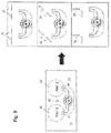
- FIG. 14 shows, in a top view, a further embodiment, in which two radiator pairs are integrated in the circuit board as an antenna array.
- FIG. 15 shows the embodiment shown in FIG. 14 , in a perspective view laterally from above, laterally from below and in a sectional view.
- FIG. 16 shows a Smith Chart as well as far field diagrams in a horizontal and in a vertical direction of the embodiment shown in FIGS. 14 and 15 .
- a coplanar stripline for supplying signals to a radiator is used for a circuit board arrangement according to the first aspect.
- FIGS. 1A and 1B show two embodiments of such a coplanar stripline.
- the coplanar stripline 1 comprises in both embodiments two conductor paths 23 and 24 arranged on a dielectric substrate 2 of the circuit board and extending at a certain distance from one another.
- One conductor path is separated from the other only by a slot 22 .
- Both conductor paths are located in the same plane, i.e. they are formed in the same metallization plane of the circuit board.
- FIGS. 1A and 1B the E-field and the H-field of such a coplanar stripline are shown.
- the E-field extends from one conductor path 23 to the other conductor path 24 .
- the H-field surrounds a respective one of the conductor paths 23 or 24 through the slot 22 .
- FIG. 1A therefore shows an embodiment in which no ground plane is located opposite the two conductor paths 23 and 24 via the dielectric 2 .
- FIG. 1B shows such an embodiment, in which the ground plane 5 is located opposite the two conductor paths 23 and 24 via the dielectric 2 .
- Such embodiments are sometimes also referred to as quasi-coplanar striplines, and also represent coplanar striplines within the meaning of the present invention.
- FIG. 2 a first embodiment of a circuit board arrangement according to the present invention in accordance with the first aspect of the present invention is now shown.
- FIG. 2 only shows the metallic parts of a field converter according to the present invention, whereas the dielectric substrate provided between the metallization planes of the circuit board is not shown for the sake of clarity.
- the field converter shown in FIG. 2 is here connected to a coplanar stripline 1 , which is shown in a shortened form in FIG. 2 , and conducts a coaxial field through the substrate of the circuit board and converts it into the coplanar stripline field of the coplanar stripline 1 .
- the field converter comprises a coaxial line section which extends through the substrate from a lower surface of the substrate to the upper surface thereof.
- the field converter comprises a coplanar conversion section defined by the metallization sections of the circuit board and connected to the coplanar stripline.
- the outer conductor of the coaxial line section is defined by vias 11 , i.e. by electrically conductive through-connections that extend through the substrate of the circuit board and surround an inner conductor 12 in the form of a ring.
- this inner conductor 12 is defined by the inner conductor of a coaxial cable, which is connected to the circuit board in the area of the field converter.
- the inner conductor may be formed by a via.
- the coplanar conversion section comprises two outer conductor sections 7 and 8 , which extend in the area of the outer conductor of the coaxial line section and are in electrical contact therewith.
- the two outer conductor sections 7 and 8 are connected to one another at one end, in area 9 .
- the respective other end of the two conductor sections 7 and 8 is connected to the two conductor paths 23 and 24 of the coplanar stripline.
- the slot 22 arranged between the conductor paths of the coplanar stripline extends into the area of the coplanar conversion section, where it extends between one of the outer conductor sections and the inner conductor 12 as slot 21 .
- the width of the slot 21 exceeds that of the slot 22 between the two conductor paths of the coplanar stripline 1 .
- the slot 21 does not extend around the entire inner conductor 12 , but is delimited by an end face 10 connecting the outer conductor section 7 to the inner conductor 12 .
- the coaxial field which the axial conductor section conducts perpendicularly through the circuit board, is blocked in a circumferential subarea and is thus converted into the coplanar stripline field, which is fed to the coplanar stripline extending along the plane of the circuit board.
- FIG. 2 shows in a first diagram 16 the coaxial field extending between the inner conductor 12 and the outer conductor 13 of the coaxial line section, and in a second diagram 17 the field, which is partially blocked by the end face 10 and which remains in the slot 21 on the plane of the coplanar conversion section.
- the field converter also serves as connection of a coaxial cable to the circuit board.
- the coaxial cable comprises an outer conductor 13 and an inner conductor 12 .
- the inner conductor 12 extends through a hole in the substrate of the circuit board up to and onto the plane of the coplanar conversion section and, in the embodiment shown, it is in contact with the end face 10 . Contacting is effected galvanically in the present embodiment.
- the outer conductor 13 of the coaxial cable ends in the area of the lower surface of the circuit board and is extended by the vias 11 , which extend through the substrate of the circuit board.
- the vias are connected to the outer conductor 13 of the coaxial cable on one side thereof and are in contact with the coplanar conversion section on the other side thereof. In particular, the vias are in contact with the two outer conductor sections 7 and 8 of the coplanar conversion section.
- the circuit board has on its lower surface a continuous metallization layer 5 , which serves as a ground plane.
- the coplanar stripline of the embodiment according to FIG. 2 is configured as shown in FIG. 1B .
- the metallization layer 5 is here electrically connected to the outer conductor 13 of the coaxial cable in area 14 and to the vias 11 in area 15 .
- FIG. 3 two embodiments of a circuit board arrangement comprising a field converter 6 according to the embodiment in FIG. 2 are now shown, the coplanar stripline 1 supplying a respective radiator 20 and 20 ′ with signals.
- the polarity of the respective radiator 20 and 20 ′ relative to the orientation of the coplanar conversion section can be selected freely.
- the antenna is not specified in detail in FIG. 3 .
- a radiator separate from the circuit board could be used, which is only fed by the circuit board arrangement according to the present invention and which is e.g. attached to the circuit board.
- the radiator is, however, defined by a metallization of the circuit board and extends preferably in the same metallization plane as the coplanar stripline 1 .
- the radiator used is here preferably a symmetrically fed differential radiator.
- the field converter has, on the one hand, the function of conducting the coaxial field through the circuit board onto the plane of the metallization, where the coplanar stripline is arranged. Furthermore, the field converter serves to connect a coaxial cable, which is perpendicularly connected to the circuit board and is extended through the circuit board by the coaxial line section of the field converter.
- the second function viz. the connection of a coaxial cable
- the coaxial line section may be used for conducting signals between different planes of a multi-layer circuit board.
- the field converter may also be used as a power divider.
- FIG. 4 shows a first embodiment of such a field converter according to the present invention, which is also used as a power divider for feeding two radiators.
- the two radiators are not shown in FIG. 4 , but they are supplied with signals by the coplanar stripline 1 and 1 ′ and are connected in parallel to the field converter.
- the field converter in FIG. 4 operates according to the same basic principle, which has already been described hereinbefore with respect to the embodiment according to FIG. 2 .
- the field converter comprises a coaxial line section, which conducts the coaxial field through a layer of the circuit board to a coplanar conversion section.
- the coaxial line section comprises a plurality of vias 11 defining the outer conductor of the coaxial line section and surrounding an inner conductor 12 of the coaxial line section.
- the coplanar conversion section comprises two outer conductor sections 7 and 8 , which extend in the area of the outer conductor of the coaxial line section and are in electrical contact therewith.
- the outer conductor section 8 merges into the first conductor path 24 of the first coplanar stripline 1
- the second outer conductor section 7 merges into the opposite second conductor path 23 ′ of the second coplanar stripline 1 ′.
- the second conductor path 23 of the first coplanar stripline 1 is connected to the opposite first conductor path 24 ′ of the second coplanar stripline 1 ′ via a diagonal path 19 of the coplanar conversion section.
- the diagonal path 19 extends radially to the coaxial line section and is connected to the inner conductor 12 .
- the field converter thus forms a power divider, which converts the coaxial field into two opposite-phase coplanar line fields 4 and 4 ′ and supplies them to the first and second coplanar striplines 1 and 1 ′.
- the slot 22 between the two conductor paths 23 and 24 of the first coplanar stripline 1 as well as the slot 22 ′ between the two stripline conductor paths 23 ′ and 24 ′ of the second coplanar stripline 1 ′ are each extended into the area between the outer conductor and the inner conductor of the coaxial line section thus forming a slot 21 and 21 ′, respectively.
- the slots 21 and 21 ′ end at the diagonal path 19 .
- the diagonal path 19 thus divides the coaxial field into two field components, which are supplied to the two coplanar striplines.
- the diagonal path 19 has the same function as the end face 10 in the embodiment shown in FIG. 2 , but is now also interrupted from the opposite side by the slot 21 ′ which extends the slot 22 ′ between the two conductor paths 23 ′ and 24 ′ of the second coplanar stripline 1 .
- the structural design of the conversion section is here preferably point symmetrical to the inner conductor 12 of the coaxial line section so as to convert the coaxial field into two coplanar stripline fields which are identical except for the phase orientation.
- the outer conductor of the coaxial line section is again defined by vias 11 connecting a metallization plane 5 on the lower surface of the substrate to the outer conductor sections 7 and 8 of the coplanar conversion section, the outer conductor sections 7 and 8 being arranged on the upper surface.
- the inner conductor is again defined by the inner conductor 12 of a coaxial cable connected to the circuit board in the area of the field converter.
- the outer conductor 13 of the coaxial cable is again connected, especially via the metallization plane 5 , to the outer conductor defined by the vias 11 .
- the structural design corresponds here to the embodiment that has already been described with respect to FIG. 2 .
- an alternative structural design is imaginable, in the case of which also the inner conductor 12 of the coaxial line section is defined by a via, and the coaxial line section is used for signal transmission between different planes of a multilayer circuit board.
- FIG. 5 shows a plurality of variants of the embodiment shown in FIG. 4 .
- the variants differ from one another, on the one hand with respect to the number of vias 11 defining the outer conductor of the coaxial line section.
- only one respective via 11 is provided in the area of the two outer conductor sections 7 and 8 .
- a plurality of vias is provided for each of the two outer conductor sections 7 and 8 .
- a respective via is also provided in the area of the diagonal path on either side.
- the vias 11 may, in addition, also extend up to and into the area of the coplanar striplines.
- the two outer conductor sections 7 and 8 are each galvanically connected to the diagonal path 19 .
- the two outer conductor sections are, however, capactively connected to the diagonal path 19 via a slot 25 and 25 ′.
- additional compensation surfaces 26 and 26 ′ are provided, via which the outer conductor paths are connected to the diagonal path.
- FIGS. 6A and 6B now show two embodiments illustrating how the vias 11 and 11 ′ are electrically contacted with the metallization sections that define the coplanar conversion section.
- contacting is effected galvanically.
- contacting between the vias 11 ′ and the metallization sections arranged in the conducting plane 30 is effected capacitively.
- the vias 11 ′ end below the metallization plane 30 and are arranged in opposed relationship with the latter with a gap 27 being formed therebetween.
- the inner conductor 12 may be coupled to the coplanar conversion section either galvanically or capacitively.
- the outer conductor of the coaxial cable could be routed through a hole in the substrate of the circuit board and form the outer conductor of the coaxial line section.
- the outer conductor may e.g. capacitively couple to the outer conductor sections of the coplanar conversion section by ending below the metallization plane 30 .
- This can be accomplished e.g. by a suitable blind hole in the substrate, or by configuring the substrate such that it is composed of two plates, which are arranged one on top of the other and only one of which is provided with the hole for the outer conductor.
- vias for the coaxial line section may also be dispensed with completely.
- FIG. 7 shows a second embodiment of a field converter 40 ′ according to the present invention, which simultaneously serves as a power divider for supplying two radiators.
- the general structural design of the field converter and power divider 40 ′ corresponds here to the first embodiment 40 of such a field converter and power divider that has already been described with respect to FIG. 4 .
- the embodiment shown in FIG. 7 converts the coaxial field supplied via the coaxial line section into two in-phase coplanar stripline fields.
- the two outer conductor sections 7 and 8 of the embodiment shown in FIG. 7 merge on both sides into a respective conductor path of a coplanar stripline.
- the first conductor path 24 of the first coplanar stripline 1 merges into the outer conductor section 8 , which, on the other side, merges into the first conductor path 24 ′ of the second coplanar stripline 1 ′.
- the opposite conductor path 23 of the first coplanar stripline 1 merges into the outer conductor section 7 and the latter merges into the first conductor path 23 ′ of the second coplanar stripline 1 ′.
- the slots 22 and 22 ′ between the respective conductor paths of the coplanar striplines merge into a common annular gap 21 ′′ provided in the area between the inner conductor 12 and the outer conductor of the coaxial line section.
- the inner conductor 12 is therefore only extended onto the plane of the metallization sections defining the coplanar conversion section, but not electrically connected to these metallization sections.
- FIGS. 8A and 8B now show the connection of two radiators 20 and 20 ′ to the embodiments of a power divider 40 and 40 ′, respectively, shown in FIGS. 4 and 7 .
- FIG. 8A shows the connection of the radiators 20 and 20 ′ to the coplanar striplines 1 and 1 ′ of the power divider shown in FIG. 4 , in the case of which the coplanar stripline fields 4 and 4 ′ are in phase opposition.
- matching circuits 31 and 31 ′ are arranged between the radiators 20 and 20 ′ and the power divider 40 .
- the matching circuits 31 and 31 ′ may here simply be defined by a suitable routing of the coplanar striplines.
- the two coplanar lines have different changes of direction so as to establish the matching circuits 31 and 31 ′.
- the field in the area of the matching circuit 31 may be rotated by 90° to the right by the first coplanar line 1
- the second coplanar stripline 1 ′ may rotate the field in the area of the matching circuit 31 ′ by 90° to the left.
- This principle shown in FIG. 8A allows the two radiators 20 and 20 ′ to be arranged side by side relatively close to each other.
- FIG. 8 b a power divider according to the embodiment in FIG. 7 is shown, in the case of which two in-phase coplanar stripline fields 4 and 4 ′ are generated.
- the two matching circuits 32 and 32 ′ which are arranged between the radiators 20 and 20 ′ and the power divider 40 ′, therefore change the orientation of the field identically and, in particular, not at all.
- the antennas 20 and 20 ′ can thus be operated in phase through the in-phase fields.
- FIG. 9 exemplarily shows once more, on the right hand side, three arrangements of dipole halves of exemplarily applicable dipoles in the embodiment according to FIG. 8A , in which two radiators 20 and 20 ′ are connected to the field converter via the matching circuits 31 and 31 ′, which are here defined by opposite direction changes of the coplanar striplines.
- radiators 33 and 33 ′ are shown, which can be used as a V-pole or as an H-pole.
- two radiators 34 and 34 ′ are shown, which can be used as a +45° pole or as a ⁇ 45° pole.
- an arrangement of two radiators 35 and 35 ′ is shown, which can again be used as a +45° pole or as a ⁇ 45° pole.
- the respective dipole halves of dipole radiators are only shown schematically, without showing the concrete connection to the coplanar striplines.
- a feature which these embodiments have in common is that the orientation of the two antennas, which are operated in parallel via the power divider, is identical. In particular, they have the same polarization plane.
- FIG. 10 shows an embodiment of a circuit board arrangement, in which the first as well as the second aspect of the present invention are realized.
- a field converter 40 is used, which feeds two radiators via coplanar striplines.
- the metallization plane 5 on the lower surface of the substrate of the circuit board serves as a reflector for the radiators 33 and 33 ′ or 34 and 34 ′ formed by the metallization plane arranged on the upper surface of the substrate.
- two dipole radiators 33 and 33 ′ are used, which are each supplied with signals from the field converter 40 via the coplanar striplines operating as matching circuits 31 and 31 ′.
- two dipole slot radiators 34 and 34 ′ are provided, which are also supplied with signals from the field converter 40 via coplanar striplines.
- the two conductor paths of the coplanar striplines merge here into a respective continuous metallization surface, so that only the slots 22 and 22 ′ of the coplanar striplines are visible.
- the elements of the coplanar conversion section of the field converter merge into the continuous metallization surface, so that also in this case only the slots 21 and 21 ′ remain.
- the two dipole elements of the dipole radiators 34 and 34 ′ extend here in an opening 35 of the metallization, so that respective slot sections are formed between the dipole elements and the metallization.
- the two radiators extend in a common polarization plane.
- the latter is offset relative to the field converter 40 and the stripline sections directly adjoining the field converter 40 .
- the radiators extend in respective parallel polarization planes which are, however, offset relative to one another.
- the centers of the two radiators are, however, again arranged in a plane, which is offset relative to the field converter 40 and the coplanar stripline sections directly adjoining the latter.
- the metallization plane 5 on the lower surface of the substrate of the circuit board serves as a reflector for the radiators 33 and 33 ′ or 34 and 34 ′.
- the thickness of the substrate between the metallization plane 5 and the metallization plane of the radiators is preferably approx. ⁇ /4, with ⁇ being the wavelength in the dielectric of the substrate of the center frequency of the lowermost resonant frequency range of the antenna. It follows that, according to the present invention, a directional radiation of the radiators will only occur towards one side, perpendicular to the plane of the circuit board.
- the metallization 5 which forms the reflector, therefore extends in the plane below the radiators 33 and 33 ′, respectively, and forms a ground plane.
- the multilayer circuit board comprises only two metallization planes and an intermediate substrate layer.
- an arrangement of the type in question is also imaginable for a multilayer circuit board comprising more than two metallization planes, so that e.g. the metallization plane defining the reflector or the metallization plane in which the radiator or the radiators are formed represents an inner metallization plane of the circuit board.
- the integrated reflector according to the second aspect may also be used independently of the use of the first aspect, i.e. the field converter 40 may also be dispensed with.
- FIG. 11 shows a further concrete embodiment of a circuit board antenna realizing both the first and the second aspect.
- the structural design of the radiators and of the reflector corresponds to the embodiment shown in FIG. 10 above.
- a frame 38 of vias 37 is provided here.
- the vias 37 extend from the reflector plane 5 to the plane of metallization in which the radiators are formed.
- the vias 37 are connected by a frame-shaped metallization section in this plane.
- the frame 38 of vias 37 may end in some other plane below or above the metallization plane in which the radiators are formed and/or begin in some other plane below or above the reflector plane 5 .
- the frame-shaped metallization section could be arranged in a metallization plane other than the metallization plane in which the radiators are formed, in particular in a metallization plane located above and/or at a short distance from the metallization plane in which the radiators are formed.
- the vias 37 and the frame-shaped metallization section also influence the antenna pattern and the S-parameters and can therefore be used e.g. for shaping the far field.
- the field converter 40 is again used to connect a coaxial cable.
- the inner conductor of the coaxial line section 12 is configured as a hollow rod into which the inner conductor of a coaxial cable can be inserted.
- a bushing 13 is provided, which is adapted to be contacted with the outer conductor of a coaxial cable. Such contacting is also possible in the case of the other embodiments of the present invention.
- FIG. 12 shows the embodiment shown in FIG. 11 with the E-field distribution in the area of the coaxial line section as well as in the area of the coplanar conversion section of the field converter.
- the box at the bottom left shows the coaxial field supplied via the coaxial cable.
- the box on the right shows the respective E-field of the coplanar conversion section at phase 0° and 90°. The conversion from the radial coaxial field into the coplanar stripline fields caused by the coplanar conversion section is clearly visible.
- FIG. 13 shows a further embodiment of a circuit board arrangement in which both aspects of the present invention are realized in combination.
- the embodiment corresponds to the embodiment in FIG. 11 .
- the field converter serves to transmit signals within the circuit board, i.e. from a first plane of the circuit board to a second or third plane of the circuit board.
- a stripline 41 is arranged in a metallization plane 45 of the circuit board, the field converter conducting the signals through at least one layer of the circuit board to the metallization plane 30 in which the radiators are arranged.
- the metallization plane 5 serving as a reflector is provided between these two metallization planes. This allows the stripline 41 to be routed in the metallization plane 45 of the circuit board independently of the position of the radiators in the metallization plane 30 .
- both the inner conductor and the outer conductor of the coaxial line section of the field converter 40 are formed by vias 11 .
- the vias 11 extend here from the metallization plane 45 of the stripline 41 to the intermediate metallization plane 5 and from there to the metallization plane 30 of the radiators.
- the stripline 41 is configured as a microstripline and coupled to the inner conductor 12 of the coaxial line section.
- the metallization plane 5 also serves as a ground plane for the microstripline 41 .
- the vias 11 surround the inner conductor in a semi-circle so that the stripline 41 can be routed out of the area of the outer conductor on the open side.
- a coplanar stripline may also be used in the metallization plane 45 so as to conduct the signals to the field converter.
- a coplanar conversion section of the type shown e.g. in FIG. 2 could be used in the metallization plane 45 .
- the structure shown in FIG. 13 requires three metallization planes of the multilayer circuit board between which dielectric substrate layers are arranged.
- the substrate layers may have different thicknesses.
- the substrate layer on the side of the ground plane 5 facing away from the radiators may be thinner than the substrate layer on the side facing the radiators, through which the distance between the radiators and the reflector is defined.
- a distribution network, matching circuits, electronic components, such as an amplifier, etc. could be provided on the side of the reflector plane 5 which faces away from the radiators and on which also the stripline 41 is provided.
- FIG. 14 shows a further embodiment, which is based on the embodiment shown in FIG. 13 and in which two antenna pairs of the type shown in FIG. 13 are connected side by side so as to form an antenna array.
- Two pairs of radiators of the type shown in FIG. 13 are here arranged side by side in a row, so that the centers of all the radiators lie on one line.
- the two pairs of radiators are each surrounded by frames 38 , so that a frame line 38 ′ is provided between the two pairs of radiators.
- the distance x1 between the two radiators 33 and 33 ′ of a radiator pair, which are supplied in common via a field converter 40 operating as a power divider, is preferably between 0.5 ⁇ and 0.9 ⁇ , e.g. 0.7 ⁇ .
- the distance x2 between neighboring radiators of two pairs of radiators is preferably between 0.5 and 0.9 ⁇ , e.g. approx. 0.8 ⁇ .
- the width W of the frame perpendicular to the orientation of the row of radiators is between 0.4 ⁇ and 0.8 ⁇ , preferably approx. 0.6 ⁇ .
- the length L of the frame in row direction for a radiator pair is between 1.2 ⁇ and 1.8 ⁇ , preferably approx. 1.5 ⁇ .
- ⁇ is here again the wavelength of the center frequency of the lowermost resonant frequency range of the radiators.
- the circuit board arrangement according to the present invention is preferably operated in the range between 3 GHz and 300 GHz, e.g. in a frequency band at 28 GHz. This results in extremely compact dimensions allowing the installation of such an array antenna also in mobile phones.
- the array antenna may, however, also be used in mobile radio base stations. In this case, the antennas are preferably arranged in rows as well as in columns next to each other.
- FIG. 15 shows the embodiment of an array antenna according to FIG. 14 in a perspective view obliquely from above, obliquely from below and in a sectional view.
- the striplines 41 which supply the two field converters 40 of the two radiator pairs with signals, are here visible.
- a supply line 42 is here provided, which merges into the supply lines 41 via a power divider. All the radiators can thus be operated in parallel. Alternatively, it would also be imaginable to supply the individual radiator pairs separately with signals and to provide separate signal lines for this purpose.
- FIG. 16 now shows on the left the Smith Chart of the antenna array shown in FIGS. 14 and 15 , and on the right the far field diagram in a horizontal and in a vertical plane. Due to the fact that the four radiators are arranged as a column antenna, the full width at half maximum of the main lobe in the vertical plane will be smaller than that in the horizontal plane.
- the radiation is emitted only to one side of the circuit board radiator.
- the reflector frame integrated in the circuit board serves to shape the far field.
Abstract
Description
Claims (18)
Applications Claiming Priority (3)
| Application Number | Priority Date | Filing Date | Title |
|---|---|---|---|
| DE102016007052.8 | 2016-06-06 | ||
| DE102016007052.8A DE102016007052A1 (en) | 2016-06-06 | 2016-06-06 | Circuit board arrangement for signal supply of a radiator |
| PCT/EP2017/000656 WO2017211451A1 (en) | 2016-06-06 | 2017-06-06 | Circuit board assembly for supplying signals to an emitter |
Publications (2)
| Publication Number | Publication Date |
|---|---|
| US20190221918A1 US20190221918A1 (en) | 2019-07-18 |
| US11289796B2 true US11289796B2 (en) | 2022-03-29 |
Family
ID=59055164
Family Applications (1)
| Application Number | Title | Priority Date | Filing Date |
|---|---|---|---|
| US16/307,442 Active 2038-12-13 US11289796B2 (en) | 2016-06-06 | 2017-06-06 | Circuit board arrangement for signal supply to a radiator |
Country Status (7)
| Country | Link |
|---|---|
| US (1) | US11289796B2 (en) |
| EP (1) | EP3449528B1 (en) |
| JP (1) | JP2019521629A (en) |
| KR (1) | KR20190015419A (en) |
| CN (1) | CN109417213B (en) |
| DE (1) | DE102016007052A1 (en) |
| WO (1) | WO2017211451A1 (en) |
Families Citing this family (2)
| Publication number | Priority date | Publication date | Assignee | Title |
|---|---|---|---|---|
| CN114512799A (en) * | 2020-11-17 | 2022-05-17 | 康普技术有限责任公司 | Antenna and methods of making and operating the same |
| US11876278B2 (en) | 2021-03-29 | 2024-01-16 | Raytheon Company | Balun comprising stepped transitions between balance and unbalance connections, where the stepped transitions include ground rings of differing lengths connected by caged vias |
Citations (25)
| Publication number | Priority date | Publication date | Assignee | Title |
|---|---|---|---|---|
| US4494083A (en) | 1981-06-30 | 1985-01-15 | Telefonaktiebolaget L M Ericsson | Impedance matching stripline transition for microwave signals |
| US4837529A (en) * | 1988-03-24 | 1989-06-06 | Honeywell, Inc. | Millimeter wave microstrip to coaxial line side-launch transition |
| US5886590A (en) * | 1997-09-04 | 1999-03-23 | Hughes Electronics Corporation | Microstrip to coax vertical launcher using fuzz button and solderless interconnects |
| US5963111A (en) * | 1998-04-09 | 1999-10-05 | Raytheon Company | Orthogonal transition from coax to stripline for opposite sides of a stripline board |
| US6025803A (en) * | 1998-03-20 | 2000-02-15 | Northern Telecom Limited | Low profile antenna assembly for use in cellular communications |
| JP2000241780A (en) | 1999-02-23 | 2000-09-08 | Ngk Insulators Ltd | Waveguide optical modulator |
| RU15150U1 (en) | 2000-02-15 | 2000-09-20 | Ростовский-на-Дону научно-исследовательский институт радиосвязи | PLANE ANTENNA ARRANGEMENT OF SLIT-RADIATED RADIATING ELEMENTS BASED ON A KOPLANAR WAVEGUIDE |
| US20040027308A1 (en) | 2002-06-10 | 2004-02-12 | Lynch Jonathan J. | Low profile, dual polarized/pattern antenna |
| US6992629B2 (en) | 2003-09-03 | 2006-01-31 | Raytheon Company | Embedded RF vertical interconnect for flexible conformal antenna |
| JP2006258762A (en) | 2005-03-18 | 2006-09-28 | Matsushita Electric Ind Co Ltd | Radar device |
| CN1937319A (en) | 2006-10-12 | 2007-03-28 | 上海交通大学 | Omnibearing/directive directional diagram reconstructable high-gain double frequency antenna |
| US20070229361A1 (en) | 2006-03-29 | 2007-10-04 | Fujitsu Component Limited | Antenna apparatus |
| US20090009399A1 (en) | 2007-07-02 | 2009-01-08 | Brian Paul Gaucher | Antenna Array Feed Line Structures For Millimeter Wave Applications |
| US20090212881A1 (en) | 2008-02-27 | 2009-08-27 | Endwave Corporation | Coaxial-to-microstrip transitions and manufacturing methods |
| US7619574B1 (en) * | 2007-09-27 | 2009-11-17 | Rockwell Collins, Inc. | Tunable antenna |
| US20100284140A1 (en) | 2006-02-20 | 2010-11-11 | Micron Technology, Inc. | Electronic device assemblies including conductive vias having two or more conductive elements |
| EP2262058A1 (en) | 2008-03-06 | 2010-12-15 | Gamma Nu, Inc. | Board-shaped wideband dual polarization antenna |
| JP2011004355A (en) | 2009-06-22 | 2011-01-06 | Sumitomo Metal Electronics Devices Inc | Structure for connecting coplanar line and coaxial line and package for high frequency using the same |
| WO2011125417A1 (en) | 2010-04-02 | 2011-10-13 | 古河電気工業株式会社 | Built-in transmitting and receiving radar antenna |
| CN102623795A (en) | 2011-01-31 | 2012-08-01 | 株式会社电装 | Antenna apparatus, radar apparatus and on-vehicle radar system |
| JP2012159349A (en) | 2011-01-31 | 2012-08-23 | Denso Corp | Antenna device, lader apparatus and vehicle-mounted lader system |
| US8350771B1 (en) * | 2009-06-02 | 2013-01-08 | The United States Of America, As Represented By The Secretary Of The Navy | Dual-band dual-orthogonal-polarization antenna element |
| CN204348905U (en) | 2014-12-04 | 2015-05-20 | 深圳市维力谷无线技术有限公司 | A kind of omnidirectional wide band high-gain PCB antenna |
| US9054403B2 (en) * | 2012-06-21 | 2015-06-09 | Raytheon Company | Coaxial-to-stripline and stripline-to-stripline transitions including a shorted center via |
| CN105024126A (en) | 2015-06-23 | 2015-11-04 | 西安空间无线电技术研究所 | Vertical coaxial-microstrip switching circuit |
-
2016
- 2016-06-06 DE DE102016007052.8A patent/DE102016007052A1/en not_active Ceased
-
2017
- 2017-06-06 US US16/307,442 patent/US11289796B2/en active Active
- 2017-06-06 KR KR1020187038224A patent/KR20190015419A/en not_active Application Discontinuation
- 2017-06-06 WO PCT/EP2017/000656 patent/WO2017211451A1/en unknown
- 2017-06-06 CN CN201780035110.3A patent/CN109417213B/en active Active
- 2017-06-06 JP JP2019516056A patent/JP2019521629A/en active Pending
- 2017-06-06 EP EP17729775.1A patent/EP3449528B1/en active Active
Patent Citations (30)
| Publication number | Priority date | Publication date | Assignee | Title |
|---|---|---|---|---|
| US4494083A (en) | 1981-06-30 | 1985-01-15 | Telefonaktiebolaget L M Ericsson | Impedance matching stripline transition for microwave signals |
| US4837529A (en) * | 1988-03-24 | 1989-06-06 | Honeywell, Inc. | Millimeter wave microstrip to coaxial line side-launch transition |
| US5886590A (en) * | 1997-09-04 | 1999-03-23 | Hughes Electronics Corporation | Microstrip to coax vertical launcher using fuzz button and solderless interconnects |
| US6025803A (en) * | 1998-03-20 | 2000-02-15 | Northern Telecom Limited | Low profile antenna assembly for use in cellular communications |
| US5963111A (en) * | 1998-04-09 | 1999-10-05 | Raytheon Company | Orthogonal transition from coax to stripline for opposite sides of a stripline board |
| JP2000241780A (en) | 1999-02-23 | 2000-09-08 | Ngk Insulators Ltd | Waveguide optical modulator |
| RU15150U1 (en) | 2000-02-15 | 2000-09-20 | Ростовский-на-Дону научно-исследовательский институт радиосвязи | PLANE ANTENNA ARRANGEMENT OF SLIT-RADIATED RADIATING ELEMENTS BASED ON A KOPLANAR WAVEGUIDE |
| US20040027308A1 (en) | 2002-06-10 | 2004-02-12 | Lynch Jonathan J. | Low profile, dual polarized/pattern antenna |
| US6992629B2 (en) | 2003-09-03 | 2006-01-31 | Raytheon Company | Embedded RF vertical interconnect for flexible conformal antenna |
| DE602004008653T2 (en) | 2003-09-03 | 2008-06-05 | Raytheon Company, Waltham | FLEXIBLE CONFORMANT ANTENNA |
| US20150319860A1 (en) | 2004-08-31 | 2015-11-05 | Micron Technology, Inc. | Electronic device assemblies including conductive vias having two or more conductive elements |
| JP2006258762A (en) | 2005-03-18 | 2006-09-28 | Matsushita Electric Ind Co Ltd | Radar device |
| US20100284140A1 (en) | 2006-02-20 | 2010-11-11 | Micron Technology, Inc. | Electronic device assemblies including conductive vias having two or more conductive elements |
| US20070229361A1 (en) | 2006-03-29 | 2007-10-04 | Fujitsu Component Limited | Antenna apparatus |
| CN1937319A (en) | 2006-10-12 | 2007-03-28 | 上海交通大学 | Omnibearing/directive directional diagram reconstructable high-gain double frequency antenna |
| US20090009399A1 (en) | 2007-07-02 | 2009-01-08 | Brian Paul Gaucher | Antenna Array Feed Line Structures For Millimeter Wave Applications |
| US7619574B1 (en) * | 2007-09-27 | 2009-11-17 | Rockwell Collins, Inc. | Tunable antenna |
| US20090212881A1 (en) | 2008-02-27 | 2009-08-27 | Endwave Corporation | Coaxial-to-microstrip transitions and manufacturing methods |
| US20110043424A1 (en) * | 2008-03-06 | 2011-02-24 | Gamma Nu, Inc. | Board-shaped wideband dual polarization antenna |
| EP2262058A1 (en) | 2008-03-06 | 2010-12-15 | Gamma Nu, Inc. | Board-shaped wideband dual polarization antenna |
| US8350771B1 (en) * | 2009-06-02 | 2013-01-08 | The United States Of America, As Represented By The Secretary Of The Navy | Dual-band dual-orthogonal-polarization antenna element |
| JP2011004355A (en) | 2009-06-22 | 2011-01-06 | Sumitomo Metal Electronics Devices Inc | Structure for connecting coplanar line and coaxial line and package for high frequency using the same |
| WO2011125417A1 (en) | 2010-04-02 | 2011-10-13 | 古河電気工業株式会社 | Built-in transmitting and receiving radar antenna |
| CN102623795A (en) | 2011-01-31 | 2012-08-01 | 株式会社电装 | Antenna apparatus, radar apparatus and on-vehicle radar system |
| DE102012201282A1 (en) | 2011-01-31 | 2012-08-02 | Denso Corporation | Antenna device, radar device and vehicle radar system |
| JP2012159349A (en) | 2011-01-31 | 2012-08-23 | Denso Corp | Antenna device, lader apparatus and vehicle-mounted lader system |
| US20150268336A1 (en) | 2011-01-31 | 2015-09-24 | Denso Corporation | Antenna apparatus, radar apparatus and on-vehicle radar system |
| US9054403B2 (en) * | 2012-06-21 | 2015-06-09 | Raytheon Company | Coaxial-to-stripline and stripline-to-stripline transitions including a shorted center via |
| CN204348905U (en) | 2014-12-04 | 2015-05-20 | 深圳市维力谷无线技术有限公司 | A kind of omnidirectional wide band high-gain PCB antenna |
| CN105024126A (en) | 2015-06-23 | 2015-11-04 | 西安空间无线电技术研究所 | Vertical coaxial-microstrip switching circuit |
Non-Patent Citations (11)
| Title |
|---|
| Examination Report for European Patent Application No. 17729775.1, dated Feb. 1, 2021, 11 pages. |
| Examination Report for European Patent Application No. 17729775.1, dated Feb. 28, 2020, 18 pages. |
| First Office Action for Chinese Patent Application No. 2017800351103, dated Aug. 24, 2020, 24 pages. |
| ISA European Patent Office, International Search Report Issued in Application No. PCT/EP2017/000656, dated Aug. 18, 2017, WIPO, 6 pages. |
| Leib, M. et al., "In-Phase and Anti-Phase Power Dividers for UWB Differentially Fed Antenna Arrays," IEEE Antennas and Wireless Propagation Letters, vol. 9. May 18, 2010, 4 pages. |
| Notice of Reasons for Refusal and Search Report for Japanese Patent Application No. 2019-516056, dated May 21, 2021, 86 pages. |
| Result of Consultation for European Patent Application No. 17729775.1, dated Sep. 13, 2021, 14 pages. |
| Search Report for Chinese Patent Application No. 2017800351103, dated Aug. 12, 2020, 2 pages. |
| Second Office Action for Chinese Patent Application No. 201780035110.3, dated Apr. 20, 2021, 23 pages. |
| Written Opinion for International Patent Application No. PCT/EP2017/000656, dated Aug. 18, 2017, 17 pages. |
| Ye, S. et al., "High Gain Planar Antenna Arrays for Mobile Satellite Communications," IEEE Antennas and Propagation Magazine, vol. 54, No. 6, Dec. 24, 2012, 9 pages. |
Also Published As
| Publication number | Publication date |
|---|---|
| US20190221918A1 (en) | 2019-07-18 |
| WO2017211451A1 (en) | 2017-12-14 |
| CN109417213B (en) | 2021-12-21 |
| DE102016007052A1 (en) | 2017-12-07 |
| JP2019521629A (en) | 2019-07-25 |
| EP3449528B1 (en) | 2022-09-14 |
| EP3449528A1 (en) | 2019-03-06 |
| CN109417213A (en) | 2019-03-01 |
| KR20190015419A (en) | 2019-02-13 |
Similar Documents
| Publication | Publication Date | Title |
|---|---|---|
| EP3166178B1 (en) | An antenna element preferably for a base station antenna | |
| US11342688B2 (en) | Dual-polarized radiating element and antenna | |
| US10396460B2 (en) | Multiband antenna and wireless communication device | |
| US11387568B2 (en) | Millimeter-wave antenna array element, array antenna, and communications product | |
| US11545761B2 (en) | Dual-band cross-polarized 5G mm-wave phased array antenna | |
| Klionovski et al. | A dual-polarization-switched beam patch antenna array for millimeter-wave applications | |
| JP2020511890A (en) | Antenna, antenna configuration method, and wireless communication device | |
| US10971824B2 (en) | Antenna element | |
| US10333228B2 (en) | Low coupling 2×2 MIMO array | |
| CN113555677B (en) | Feed system, antenna system and base station | |
| JP2004120733A (en) | Stripline parallel-series-fed proximity coupled cavity backed patch antenna array | |
| US20190044234A1 (en) | Tripole current loop radiating element with integrated circularly polarized feed | |
| KR101992620B1 (en) | The Antenna with High Gain and Omni-Directional characteristics | |
| US11217903B2 (en) | Antenna system for a wireless communication device | |
| US11289796B2 (en) | Circuit board arrangement for signal supply to a radiator | |
| US10461417B2 (en) | Power feed circuit and antenna device | |
| KR101833037B1 (en) | Multi Polarized Antenna | |
| US20150372377A1 (en) | Dipole antenna array | |
| KR20190087270A (en) | Antenna device and electronic apparatus having the same | |
| JP2008244733A (en) | Planar array antenna system and radio communication equipment with the same | |
| WO2022102518A1 (en) | Dipole antenna, polarization shared antenna, and array antenna | |
| RU2771751C2 (en) | Power circuit of base station antenna, base station antenna and base station | |
| N’Gom et al. | Design of an adaptive subarray antenna for multibeams wireless small cell backhaul in mmWave | |
| WO2023117097A1 (en) | Antenna and cell site | |
| WO2023117096A1 (en) | Antenna with dual polarized radiators |
Legal Events
| Date | Code | Title | Description |
|---|---|---|---|
| AS | Assignment |
Owner name: KATHREIN SE, GERMANY Free format text: ASSIGNMENT OF ASSIGNORS INTEREST;ASSIGNORS:VOLLMER, ANDREAS;FLEANCU, DAN;REEL/FRAME:047684/0898 Effective date: 20181119 |
|
| FEPP | Fee payment procedure |
Free format text: ENTITY STATUS SET TO UNDISCOUNTED (ORIGINAL EVENT CODE: BIG.); ENTITY STATUS OF PATENT OWNER: LARGE ENTITY |
|
| STPP | Information on status: patent application and granting procedure in general |
Free format text: DOCKETED NEW CASE - READY FOR EXAMINATION |
|
| AS | Assignment |
Owner name: ERICSSON AB, SWEDEN Free format text: ASSIGNMENT OF ASSIGNORS INTEREST;ASSIGNOR:KATHREIN SE;REEL/FRAME:053798/0470 Effective date: 20191001 Owner name: TELEFONAKTIEBOLAGET LM ERICSSON (PUBL), SWEDEN Free format text: ASSIGNMENT OF ASSIGNORS INTEREST;ASSIGNOR:ERICSSON AB;REEL/FRAME:053816/0791 Effective date: 20191001 |
|
| STPP | Information on status: patent application and granting procedure in general |
Free format text: NON FINAL ACTION MAILED |
|
| STPP | Information on status: patent application and granting procedure in general |
Free format text: FINAL REJECTION MAILED |
|
| STPP | Information on status: patent application and granting procedure in general |
Free format text: RESPONSE AFTER FINAL ACTION FORWARDED TO EXAMINER |
|
| STPP | Information on status: patent application and granting procedure in general |
Free format text: NOTICE OF ALLOWANCE MAILED -- APPLICATION RECEIVED IN OFFICE OF PUBLICATIONS |
|
| STPP | Information on status: patent application and granting procedure in general |
Free format text: NOTICE OF ALLOWANCE MAILED -- APPLICATION RECEIVED IN OFFICE OF PUBLICATIONS |
|
| STPP | Information on status: patent application and granting procedure in general |
Free format text: PUBLICATIONS -- ISSUE FEE PAYMENT VERIFIED |
|
| STCF | Information on status: patent grant |
Free format text: PATENTED CASE |