WO2010055754A1 - 熱電変換モジュール及び熱電変換装置 - Google Patents
熱電変換モジュール及び熱電変換装置 Download PDFInfo
- Publication number
- WO2010055754A1 WO2010055754A1 PCT/JP2009/068140 JP2009068140W WO2010055754A1 WO 2010055754 A1 WO2010055754 A1 WO 2010055754A1 JP 2009068140 W JP2009068140 W JP 2009068140W WO 2010055754 A1 WO2010055754 A1 WO 2010055754A1
- Authority
- WO
- WIPO (PCT)
- Prior art keywords
- conversion module
- thermoelectric conversion
- substrate
- thermoelectric
- type semiconductor
- Prior art date
Links
Images


Classifications
-
- H—ELECTRICITY
- H01—ELECTRIC ELEMENTS
- H01L—SEMICONDUCTOR DEVICES NOT COVERED BY CLASS H10
- H01L23/00—Details of semiconductor or other solid state devices
- H01L23/34—Arrangements for cooling, heating, ventilating or temperature compensation ; Temperature sensing arrangements
- H01L23/38—Cooling arrangements using the Peltier effect
-
- H—ELECTRICITY
- H10—SEMICONDUCTOR DEVICES; ELECTRIC SOLID-STATE DEVICES NOT OTHERWISE PROVIDED FOR
- H10N—ELECTRIC SOLID-STATE DEVICES NOT OTHERWISE PROVIDED FOR
- H10N10/00—Thermoelectric devices comprising a junction of dissimilar materials, i.e. devices exhibiting Seebeck or Peltier effects
- H10N10/10—Thermoelectric devices comprising a junction of dissimilar materials, i.e. devices exhibiting Seebeck or Peltier effects operating with only the Peltier or Seebeck effects
- H10N10/17—Thermoelectric devices comprising a junction of dissimilar materials, i.e. devices exhibiting Seebeck or Peltier effects operating with only the Peltier or Seebeck effects characterised by the structure or configuration of the cell or thermocouple forming the device
-
- H—ELECTRICITY
- H01—ELECTRIC ELEMENTS
- H01L—SEMICONDUCTOR DEVICES NOT COVERED BY CLASS H10
- H01L2924/00—Indexing scheme for arrangements or methods for connecting or disconnecting semiconductor or solid-state bodies as covered by H01L24/00
- H01L2924/0001—Technical content checked by a classifier
- H01L2924/0002—Not covered by any one of groups H01L24/00, H01L24/00 and H01L2224/00
-
- H—ELECTRICITY
- H01—ELECTRIC ELEMENTS
- H01S—DEVICES USING THE PROCESS OF LIGHT AMPLIFICATION BY STIMULATED EMISSION OF RADIATION [LASER] TO AMPLIFY OR GENERATE LIGHT; DEVICES USING STIMULATED EMISSION OF ELECTROMAGNETIC RADIATION IN WAVE RANGES OTHER THAN OPTICAL
- H01S5/00—Semiconductor lasers
- H01S5/02—Structural details or components not essential to laser action
- H01S5/022—Mountings; Housings
- H01S5/02208—Mountings; Housings characterised by the shape of the housings
- H01S5/02212—Can-type, e.g. TO-CAN housings with emission along or parallel to symmetry axis
-
- H—ELECTRICITY
- H01—ELECTRIC ELEMENTS
- H01S—DEVICES USING THE PROCESS OF LIGHT AMPLIFICATION BY STIMULATED EMISSION OF RADIATION [LASER] TO AMPLIFY OR GENERATE LIGHT; DEVICES USING STIMULATED EMISSION OF ELECTROMAGNETIC RADIATION IN WAVE RANGES OTHER THAN OPTICAL
- H01S5/00—Semiconductor lasers
- H01S5/02—Structural details or components not essential to laser action
- H01S5/024—Arrangements for thermal management
- H01S5/02407—Active cooling, e.g. the laser temperature is controlled by a thermo-electric cooler or water cooling
- H01S5/02415—Active cooling, e.g. the laser temperature is controlled by a thermo-electric cooler or water cooling by using a thermo-electric cooler [TEC], e.g. Peltier element
Definitions
- the present invention relates to a thermoelectric conversion module having a thermoelectric element utilizing a thermoelectric effect and a thermoelectric conversion device.
- thermoelectric conversion modules such as a cooling module and a power generation module that mutually convert thermal energy and electrical energy using thermoelectric effects such as the Thomson effect, Peltier effect, Seebeck effect, and the like are known.
- a thermoelectric conversion module can be realized, for example, by providing a P-type semiconductor and an N-type semiconductor as a pair of thermoelectric elements on a semiconductor substrate.
- the thermoelectric conversion module may be provided with a heat sink for radiating the heat of the thermoelectric conversion module to the outside.
- thermoelectric conversion module has a problem that heat dissipation is poor because the heat dissipation of the thermoelectric conversion module itself is not sufficiently considered.
- the conventional heat conversion module requires a heat radiating member such as a heat sink for the purpose of improving heat dissipation, and cannot be applied to a mobile device such as a mobile phone that is required to be small or thin.
- an object of the present invention is to provide a thermoelectric conversion module and a thermoelectric conversion device with improved heat dissipation.
- an embodiment of the present invention includes a substrate on which a first thermoelectric element that moves heat by electric energy or a second thermoelectric element that converts heat energy into electric energy is disposed, And a heat exchanging member disposed on the first or second thermoelectric element, wherein the substrate has a heat dissipation structure.
- the embodiment of the present invention includes a substrate on which a first thermoelectric element that moves heat by electric energy or a second thermoelectric element that converts heat energy to electric energy is disposed, and the first or second A heat exchange member disposed on the thermoelectric element, and an electrode is formed on a surface side of the substrate opposite to the surface side on which the first or second thermoelectric element is provided, A thermoelectric conversion module is provided that is electrically connected to the first or second thermoelectric element through a through hole penetrating the substrate.
- the embodiment of the present invention includes a substrate on which a first thermoelectric element that transfers heat by electric energy or a second thermoelectric element that converts heat energy to electric energy is disposed, and the first or second A heat exchange member disposed on the thermoelectric element, and a groove is formed on a side surface of the substrate, and the groove is a conductive material electrically connected to the first or second thermoelectric element.
- a thermoelectric conversion module characterized in that a body is formed is provided.
- thermoelectric conversion module In the embodiment of the present invention, a first thermoelectric element that moves heat by electric energy and a second thermoelectric element that converts heat energy into electric energy are disposed between a substrate and a heat exchange member.
- a thermoelectric conversion module is provided.
- the embodiment of the present invention includes a first thermoelectric element that is composed of a first conductivity type semiconductor and a second conductivity type semiconductor and moves heat by electric energy, and the first conductivity type semiconductor and the second conductivity type semiconductor.
- a second thermoelectric element that converts thermal energy into electric energy is disposed between a substrate and a heat exchange member, and the first thermoelectric element includes the first conductive semiconductor.
- a thermoelectric conversion device having a power supply for applying a voltage so that the potential of the second conductive type semiconductor becomes higher than the potential of the second conductive semiconductor, and a load connected to the second thermoelectric element.
- the embodiment of the present invention also includes a first thermoelectric element that is composed of a first conductive semiconductor and a second conductive semiconductor and moves heat by electric energy, and the first conductive semiconductor and the second conductive semiconductor. And a second thermoelectric element that converts thermal energy into electric energy is disposed between a substrate and a heat exchange member, and the first thermoelectric element includes the first conductive semiconductor.
- a variable power supply that applies a voltage so that the potential of the second conductive semiconductor is higher than the potential of the second conductive semiconductor, a load connected to the second thermoelectric element, and a current output from the second thermoelectric element or Based on the detection unit for detecting the voltage and the detection result of the detection unit, the temperature on the heat exchange member side of the first thermoelectric element is calculated, and the variable power supply is controlled so that the temperature becomes a predetermined temperature.
- Control voltage Providing a thermoelectric conversion device and having a control unit.
- thermoelectric conversion module and a thermoelectric conversion device with improved heat dissipation.
- thermoelectric conversion module 1 is a perspective view (part 1) illustrating a thermoelectric conversion module according to a first embodiment of the invention; It is a perspective view (the 2) which illustrates the thermoelectric conversion module which concerns on the 1st Embodiment of this invention.
- 1 is a cross-sectional view illustrating a thermoelectric conversion module according to a first embodiment of the invention. It is FIG. (The 1) which illustrates the manufacturing process of the thermoelectric conversion module which concerns on the 1st Embodiment of this invention. It is FIG. (The 2) which illustrates the manufacturing process of the thermoelectric conversion module which concerns on the 1st Embodiment of this invention. It is FIG. (The 3) which illustrates the manufacturing process of the thermoelectric conversion module which concerns on the 1st Embodiment of this invention.
- FIG. (The 4) which illustrates the manufacturing process of the thermoelectric conversion module which concerns on the 1st Embodiment of this invention.
- FIG. 7 is a diagram (No. 5) illustrating the manufacturing process of the thermoelectric conversion module according to the first embodiment of the invention; It is FIG. (6) which illustrates the manufacturing process of the thermoelectric conversion module which concerns on the 1st Embodiment of this invention. It is FIG. (The 7) which illustrates the manufacturing process of the thermoelectric conversion module which concerns on the 1st Embodiment of this invention. It is FIG. (The 8) which illustrates the manufacturing process of the thermoelectric conversion module which concerns on the 1st Embodiment of this invention.
- thermoelectric conversion module which concerns on the 1st Embodiment of this invention.
- FIG. (The 10) which illustrates the manufacturing process of the thermoelectric conversion module which concerns on the 1st Embodiment of this invention.
- FIG. (the 11) which illustrates the manufacturing process of the thermoelectric conversion module which concerns on the 1st Embodiment of this invention.
- FIG. (the 12) which illustrates the manufacturing process of the thermoelectric conversion module which concerns on the 1st Embodiment of this invention.
- FIG. (The 13) which illustrates the manufacturing process of the thermoelectric conversion module which concerns on the 1st Embodiment of this invention.
- thermoelectric conversion module which concerns on the 1st Embodiment of this invention.
- the 1st Embodiment of this invention It is a perspective view (the 1) which illustrates the thermoelectric conversion module which concerns on the 2nd Embodiment of this invention.
- the 2 which illustrates the thermoelectric conversion module which concerns on the 2nd Embodiment of this invention.
- the 1 which illustrates the manufacturing process of the thermoelectric conversion module which concerns on the 2nd Embodiment of this invention.
- FIG. (The 2) which illustrates the manufacturing process of the thermoelectric conversion module which concerns on the 2nd Embodiment of this invention.
- FIG. 1 which illustrates the thermoelectric conversion module which concerns on the 2nd Embodiment of this invention.
- the 2nd Embodiment of this invention It is a circuit diagram for demonstrating operation
- thermoelectric conversion module 2 is a diagram (part 1) illustrating a state in which a thermoelectric conversion module is arranged on a heating element. It is a perspective view (the 1) which illustrates the thermoelectric conversion module which concerns on the modification of the 2nd Embodiment of this invention. It is a perspective view (the 2) which illustrates the thermoelectric conversion module which concerns on the modification of the 2nd Embodiment of this invention. It is sectional drawing which illustrates the thermoelectric conversion module which concerns on the modification of the 2nd Embodiment of this invention. It is a figure which illustrates the manufacturing process of the thermoelectric conversion module which concerns on the modification of the 2nd Embodiment of this invention. FIG.
- thermoelectric conversion module 3 is a diagram (part 2) illustrating a state in which a thermoelectric conversion module is arranged on a heating element. It is a perspective view (the 1) which illustrates the thermoelectric conversion module which concerns on the 3rd Embodiment of this invention. It is a perspective view (the 2) which illustrates the thermoelectric conversion module which concerns on the 3rd Embodiment of this invention. It is sectional drawing which illustrates the thermoelectric conversion module which concerns on the 3rd Embodiment of this invention. It is FIG. (The 1) which illustrates the manufacturing process of the thermoelectric conversion module which concerns on the 3rd Embodiment of this invention. It is FIG. (The 2) which illustrates the manufacturing process of the thermoelectric conversion module which concerns on the 3rd Embodiment of this invention.
- FIG. (The 3) which illustrates the manufacturing process of the thermoelectric conversion module which concerns on the 3rd Embodiment of this invention.
- FIG. (The 4) which illustrates the manufacturing process of the thermoelectric conversion module which concerns on the 3rd Embodiment of this invention.
- FIG. (The 5) which illustrates the manufacturing process of the thermoelectric conversion module which concerns on the 3rd Embodiment of this invention.
- FIG. (The 6) which illustrates the manufacturing process of the thermoelectric conversion module which concerns on the 3rd Embodiment of this invention.
- FIG. (The 7) which illustrates the manufacturing process of the thermoelectric conversion module which concerns on the 3rd Embodiment of this invention. It is FIG.
- thermoelectric conversion module which concerns on the 3rd Embodiment of this invention.
- FIG. (The 9) which illustrates the manufacturing process of the thermoelectric conversion module which concerns on the 3rd Embodiment of this invention.
- FIG. (The 10) which illustrates the manufacturing process of the thermoelectric conversion module which concerns on the 3rd Embodiment of this invention.
- FIG. (The 11) which illustrates the manufacturing process of the thermoelectric conversion module which concerns on the 3rd Embodiment of this invention.
- FIG. (The 12) which illustrates the manufacturing process of the thermoelectric conversion module which concerns on the 3rd Embodiment of this invention.
- FIG. 6 is a diagram (part 3) illustrating a state in which a thermoelectric conversion module is arranged on a heating element; It is a circuit diagram for demonstrating the thermoelectric conversion apparatus which applied the thermoelectric conversion module which concerns on the 3rd Embodiment of this invention.
- FIG. 6 is a diagram (part 4) illustrating a state in which a thermoelectric conversion module is arranged on a heating element;
- thermoelectric conversion module According to First Embodiment of the Present Invention
- FIG. 1 is a perspective view (part 1) illustrating a thermoelectric conversion module according to a first embodiment of the invention.
- FIG. 2 is a perspective view (part 2) illustrating the thermoelectric conversion module according to the first embodiment of the invention.
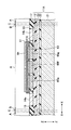
- FIG. 3 is a cross-sectional view illustrating the thermoelectric conversion module according to the first embodiment of the invention.
- FIG. 3 shows a cross section parallel to the XZ plane passing through electrodes 14a and 14b described later in FIGS.
- the thermoelectric conversion module 10 includes a substrate 11, a first wiring pattern 13, electrodes 14a and 14b, P-type semiconductors 15a and 15b, and an N-type semiconductor 16a (see FIG. 11). And 16b, a second insulating layer 17, a second wiring pattern 18, and a substrate 19.
- the second insulating layer 17 is drawn transparently for convenience in order to make the structure easy to understand. The arrangement of the P-type semiconductor 15a and the N-type semiconductor 16a, and the P-type semiconductor 15b and the N-type semiconductor 16b is shown in FIG.
- the first wiring pattern 13 is formed on one surface of the substrate 11 (the surface on the first insulating layer 12 side described later).
- the substrate 11 will be described later.
- the thickness of the first wiring pattern 13 can be set to about 0.2 ⁇ m, for example.
- Electrodes 14 a and 14 b are formed on the first wiring pattern 13.
- the thickness of the electrodes 14a and 14b can be about 10 ⁇ m, for example.
- a P-type semiconductor 15a and an N-type semiconductor 16a are formed on the first wiring pattern 13, a P-type semiconductor 15a and an N-type semiconductor 16a (see FIG. 11), a P-type semiconductor 15b, and an N-type semiconductor 16b are formed.
- a second insulating layer 17 is formed in portions excluding the electrodes 14a and 14b, the P-type semiconductor 15a and the N-type semiconductor 16a, and the P-type semiconductor 15b and the N-type semiconductor 16b on the first insulating layer 12 and the first wiring pattern 13.
- the second insulating layer 17 can be, for example, a silicon oxide film (SiO 2 ).
- the thickness of the second insulating layer 17 can be about 10.2 ⁇ m, for example.
- the upper surfaces of the electrodes 14a and 14b, the upper surfaces of the P-type semiconductor 15a and the N-type semiconductor 16a, and the P-type semiconductor 15b and the N-type semiconductor 16b are exposed from the second insulating layer 17.
- the P-type semiconductor 15a and the N-type semiconductor 16a constitute a pair of thermoelectric elements.
- the P-type semiconductor 15a and the N-type semiconductor 16a which are a pair of thermoelectric elements, cause a current to flow from the N-type semiconductor 16a side to the P-type semiconductor 15a side by making the potential of the N-type semiconductor 16a higher than the potential of the P-type semiconductor 15a.
- the thermoelectric element functions as a thermoelectric element (Peltier element) that transfers heat by electric energy. That is, the P-type semiconductor 15a and the N-type semiconductor 16a, which are a pair of thermoelectric elements, have a function of cooling the heating element.
- the P-type semiconductor 15b and the N-type semiconductor 16b also constitute a pair of thermoelectric elements, and have the same functions as the P-type semiconductor 15a and the N-type semiconductor 16a that are the pair of thermoelectric elements.
- the lower surface of the P-type semiconductor 15 a is electrically connected to the electrode 14 a by the first wiring pattern 13.
- the lower surface of the N-type semiconductor 16 b is electrically connected to the electrode 14 b by the first wiring pattern 13.
- the lower surface of the P-type semiconductor 15 b is electrically connected to the lower surface of the N-type semiconductor 16 a by the first wiring pattern 13.
- As a material of the P-type semiconductors 15a and 15b for example, Bi 0.5 Te 3 Sb 1.5 can be used.
- As a material of the N-type semiconductors 16a and 16b for example, Bi 2 Te 2.7 Se 0.3 can be used.
- the thicknesses of the P-type semiconductor 15a and the N-type semiconductor 16a, and the P-type semiconductor 15b and the N-type semiconductor 16b can be set to about 10 ⁇ m, for example.
- a second wiring pattern 18 is formed on the P-type semiconductor 15a and the N-type semiconductor 16a, and on the P-type semiconductor 15b and the N-type semiconductor 16b.
- the upper surface of the P-type semiconductor 15a is electrically connected to the upper surface of the N-type semiconductor 16a disposed adjacent to the P-type semiconductor 15a in the Y direction by the second wiring pattern 18.
- the upper surface of the N-type semiconductor 16 b is electrically connected to the upper surface of the P-type semiconductor 15 b disposed adjacent to the N-type semiconductor 16 b in the Y direction by the second wiring pattern 18.
- As a material of the second wiring pattern 18, for example, Cu or the like can be used.
- the thickness of the second wiring pattern 18 can be set to about 0.2 ⁇ m, for example.
- the pair of thermoelectric elements P-type semiconductor 15a and N-type semiconductor 16a and the pair of thermoelectric elements P-type semiconductor 15b and N-type semiconductor 16b are connected in series by the first wiring pattern 13 and the second wiring pattern 18. It is connected to the.
- the pair of thermoelectric elements P-type semiconductor 15a and N-type semiconductor 16a and the pair of thermoelectric elements P-type semiconductor 15b and N-type semiconductor 16b each have a function of cooling the heating element. A similar function is also obtained when these are connected in series.
- two pairs of P-type semiconductors and N-type semiconductors are connected in series, but only one set may be used, or three or more sets may be connected in series.
- the amount of heat absorbed by the thermoelectric element is determined by the area of the thermoelectric element. Therefore, if a pair of P-type semiconductor and N-type semiconductor, which are thermoelectric elements, is used in only one set, and if two or more sets are connected in series, the endothermic amount is the same. Will not change. In addition, the power required for endotherm does not change. However, by increasing the number of pairs in which a pair of P-type semiconductors and N-type semiconductors that are thermoelectric elements are connected in series, the voltage required for heat absorption increases and the current decreases (power is constant). Therefore, for example, the number of pairs in which a pair of P-type semiconductors and N-type semiconductors that are thermoelectric elements are connected in series may be determined so as to operate at a voltage that matches the specifications of the power supply.
- either the P-type semiconductor or the N-type semiconductor may be referred to as a first conductivity type semiconductor.
- the second conductivity type semiconductor indicates a conductivity type opposite to the first conductivity type semiconductor.
- a substrate 19 that is a heat exchange member is formed on the second wiring pattern 18.
- a material of the substrate 19 for example, silicon can be used.
- the thickness t 1 of the substrate 19 can be set to about 0.15 mm, for example.
- the width W 1 of the substrate 19 may be, for example, about 0.75 mm.
- Depth D 1 of the substrate 19 may be, for example, about 0.55 mm.
- the substrate 11 is, for example, a first insulating layer 12 formed on one surface of a so-called SOI (Silicon On Insulator) substrate.
- the first insulating layer 12 can be, for example, a silicon thermal oxide film (SiO 2 ).
- the thickness of the first insulating layer 12 can be about 1 ⁇ m, for example.
- a so-called SOI (Silicon On Insulator) substrate has a structure in which a third insulating layer 22 and a silicon active layer 23 are stacked on a silicon substrate 21.
- the thickness t 2 of the substrate 11 may be, for example, about 0.25 mm.
- the width W 2 of the substrate 11 may be, for example, about 2 mm.
- Depth D 2 of the substrate 11 may be, for example, about 1 mm.
- a heat dissipation mechanism 21a is formed in the vicinity of the portion of the silicon substrate 21 that overlaps the substrate 19 in plan view.
- the heat dissipation mechanism 21a has a plurality of protrusions 21b.
- the thickness t 3 of the protrusion 21b may be, for example, about 0.15 mm.
- Width W 3 of the protruding portion 21b may be, for example, about 0.1 mm.
- Depth D 3 of the protrusion 21b may be, for example, about 0.1 mm.
- Pitch P 3 of the protrusion 21b may be, for example, about 0.2 mm.
- thermoelectric conversion module According to First Embodiment of the Present Invention
- FIGS. 4 to 16 are diagrams illustrating the manufacturing process of the thermoelectric conversion module according to the first embodiment of the invention. 4 to 16, the same components as those of the thermoelectric conversion module 10 shown in FIGS. 1 to 3 are denoted by the same reference numerals, and the description thereof may be omitted.
- SOI Silicon on Insulator
- FIGS. 4 to 16 are diagrams illustrating the manufacturing process of the thermoelectric conversion module according to the first embodiment of the invention. 4 to 16, the same components as those of the thermoelectric conversion module 10 shown in FIGS. 1 to 3 are denoted by the same reference numerals, and the description thereof may be omitted.
- SOI Silicon-On Insulator
- FIG. 4 is a plan view illustrating the substrate 20
- FIG. 5 is a cross-sectional view illustrating the substrate 20.
- the substrate 20 includes a plurality of regions A (hereinafter referred to as “thermoelectric conversion module formation regions A”) that form the thermoelectric conversion module 10 and a region B (hereinafter referred to as “dicing region”) that separates the plurality of thermoelectric conversion module formation regions A. B ”). C in the dicing area B indicates a position where the dicing blade or the like cuts the substrate 20 (hereinafter referred to as “substrate cutting position C”).
- the substrate 20 shown in FIGS. 4 and 5 is formed with a first insulating layer 12 on one surface to become a substrate 11A to be described later, and then cut at a substrate cutting position C, whereby the substrate 11 described above (FIG. 1 to FIG. 3).
- the third insulating layer 22 is a silicon oxide film (SiO 2 ), and the thickness thereof can be, for example, about 0.5 ⁇ m.
- a so-called SOI (Silicon On Insulator) substrate is formed by implanting oxygen ions from one surface of a silicon single crystal wafer (silicon active layer 23 and silicon substrate 21) to form an oxygen ion implanted layer. It can be manufactured by changing the quality of the injection layer into a silicon oxide film (third insulating layer 22).
- a silicon oxide film (third insulating layer 22) is formed on the silicon single crystal wafer (silicon active layer 23) by a method such as thermal oxidation, and the silicon single crystal wafer (silicon active layer 23) is converted into a silicon oxide film (third oxide film).
- it may be produced by being attached on a separately prepared base wafer (silicon substrate 21) via an insulating layer 22).
- the first insulating layer 12 is formed on one surface of the substrate 20 (the surface on the silicon active layer 23 side), and the substrate 11A is manufactured.
- the thickness of the first insulating layer 12 can be set to about 0.5 ⁇ m, for example.
- the first insulating layer 12 can be, for example, a silicon oxide film (SiO 2 ).
- the first insulating layer 12 can be formed by thermally oxidizing the upper surface of the silicon active layer 23 made of, for example, silicon.
- the first insulating layer 12 may be formed by depositing a silicon oxide film (SiO 2 ) on the upper surface of the silicon active layer 23 by, eg, CVD.
- a heat dissipation mechanism 21 a is formed on the silicon substrate 21.
- the heat dissipation mechanism 21a is formed in the vicinity of a portion of the silicon substrate 21 that overlaps a substrate 19 described later in plan view.
- the heat dissipating mechanism 21 a is formed by forming a plurality of protrusions 21 b on the silicon substrate 21.
- the plurality of protrusions 21b can be formed using, for example, a Bosch process by deep RIE (Reactive Ion Etching) which is a MEMS technique.
- Deep RIE is a type of dry etching, and the Bosch process performs anisotropic plasma etching by supplying SF 6 and C 4 F 8 alternately in the plasma atmosphere at intervals of several seconds to several tens of seconds. It is. Since the third insulating layer 22 functions as an etching stop layer during deep RIE, the plurality of protrusions 21 b are formed only on one side of the third insulating layer 22 of the silicon substrate 21.
- the thickness t 3 of the protrusion 21b may be, for example, about 0.24 mm.
- Width W 3 of the protruding portion 21b may be, for example, about 0.1 mm.
- the depth D 3 (not shown) of the protrusion 21b can be set to about 0.1 mm, for example.
- Pitch P 3 of the protrusion 21b may be, for example, about 0.2 mm.
- FIG. 8 is a plan view
- FIG. 9 is a cross-sectional view taken along the line DD of FIG.
- the first wiring pattern 13 is formed as shown below, for example.
- a first metal layer made of Cu or the like is formed on the first insulating layer 12 by sputtering or the like.
- the first metal layer for example, a laminated body composed of a Cu layer and a Ti layer may be used.
- a second metal layer made of Cu or the like is formed on the first metal layer by electrolytic plating using the first metal layer as a power feeding layer, for example.
- the resist film is exposed and developed by a photolithography method, and the resist film is applied only to a portion corresponding to the formation region of the first wiring pattern 13 on the second metal layer.
- the first metal layer and the second metal layer are etched using the resist film as a mask, and the portions of the first metal layer and the second metal layer where the resist film is not formed are removed. Thereafter, the resist film is removed. Thereby, the 1st wiring pattern 13 which consists of a 1st metal layer and a 2nd metal layer is formed.
- the thickness of the first wiring pattern 13 can be set to about 0.2 ⁇ m, for example.
- electrodes 14 a and 14 b are formed on the first wiring pattern 13.
- the electrodes 14a and 14b are formed as shown below, for example.
- a resist film is applied on the first insulating layer 12 so as to cover the first wiring pattern 13.
- the resist film is exposed and developed by a photolithography method, and an opening is formed so as to expose the first wiring pattern 13 in a portion corresponding to the formation region of the electrodes 14a and 14b.
- electrodes 14a and 14b made of Cu or the like are formed by electrolytic plating using the first wiring pattern 13 as a power feeding layer, for example. Thereafter, the resist film is removed. Thereby, electrodes 14 a and 14 b are formed on the first wiring pattern 13.
- the thickness of the electrodes 14a and 14b can be about 10 ⁇ m, for example.
- Au plating may be applied to the surfaces of the electrodes 14a and 14b.
- FIG. 11 is a plan view
- FIG. 12 is a cross-sectional view taken along the line DD of FIG.
- the P-type semiconductor 15a and the N-type semiconductor 16a, and the P-type semiconductor 15b and the N-type semiconductor 16b are formed as follows, for example. First, a resist film is applied on the first insulating layer 12 so as to cover the first wiring pattern 13 and the electrodes 14a and 14b. Then, the resist film is exposed and developed by a photolithography method, and an opening is formed so as to expose the first wiring pattern 13 in a portion corresponding to the formation region of the P-type semiconductors 15a and 15b. Next, P-type semiconductors 15a and 15b are formed in the openings of the resist film, for example, by sputtering.
- a resist film is applied so as to cover the P-type semiconductors 15a and 15b, the resist film is exposed and developed by photolithography, and the first wiring pattern 13 is formed in a portion corresponding to the formation region of the N-type semiconductors 16a and 16b.
- An opening is formed so as to be exposed.
- N-type semiconductors 16a and 16b are formed in the openings of the resist film, for example, by sputtering.
- the resist film is removed.
- the P-type semiconductor 15a and the N-type semiconductor 16a, and the P-type semiconductor 15b and the N-type semiconductor 16b are formed on the first wiring pattern 13.
- a vacuum deposition method, an ion plating method, or the like may be used.
- the lower surface of the P-type semiconductor 15 a is electrically connected to the electrode 14 a by the first wiring pattern 13.
- the lower surface of the N-type semiconductor 16 b is electrically connected to the electrode 14 b by the first wiring pattern 13.
- the lower surface of the P-type semiconductor 15 b is electrically connected to the lower surface of the N-type semiconductor 16 a by the first wiring pattern 13.
- Bi 0.5 Te 3 Sb 1.5 can be used.
- As a material of the N-type semiconductors 16a and 16b for example, Bi 2 Te 2.7 Se 0.3 can be used.
- the thicknesses of the P-type semiconductors 15a and 15b and the N-type semiconductors 16a and 16b can be set to about 10 ⁇ m, for example.
- FIGS. 13 and 14 are plan views
- FIG. 14 is a cross-sectional view taken along the line DD of FIG.
- the second wiring pattern 18 is formed, for example, as shown below.
- the second insulating layer 17 is formed on the first insulating layer 12 so as to cover the first wiring pattern 13, the electrodes 14a and 14b, the P-type semiconductors 15a and 15b, and the N-type semiconductors 16a and 16b.
- the second insulating layer 17 can be, for example, a silicon oxide film (SiO 2 ).
- the upper surface of the second insulating layer 17 is polished by CMP or the like to expose the upper surfaces of the electrodes 14a and 14b, the upper surfaces of the P-type semiconductors 15a and 15b, and the N-type semiconductors 16a and 16b.
- the second wiring pattern 18 is formed on the exposed P-type semiconductors 15a and 15b and the N-type semiconductors 16a and 16b.
- the second wiring pattern 18 can be formed by the same method as the first wiring pattern 13, the description thereof is omitted.
- a material of the second wiring pattern 18 for example, Cu or the like can be used.
- the thickness of the second wiring pattern 18 can be set to about 0.2 ⁇ m, for example.
- the upper surface of the P-type semiconductor 15 a is electrically connected to the upper surface of the N-type semiconductor 16 a disposed adjacent to the P-type semiconductor 15 a in the Y direction by the second wiring pattern 18.
- the upper surface of the N-type semiconductor 16 b is electrically connected to the upper surface of the P-type semiconductor 15 b disposed adjacent to the N-type semiconductor 16 b in the Y direction by the second wiring pattern 18.
- FIG. 15 is a plan view
- FIG. 16 is a cross-sectional view taken along the line DD in FIG.
- the substrate 19 is formed on the second wiring pattern 18 by, for example, room temperature bonding.
- the room temperature bonding is a method in which the contact surface between the second wiring pattern 18 and the substrate 19 is flattened so that atoms are exposed on the surface and bonded by atomic force.
- a material of the substrate 19 for example, silicon can be used.
- the thickness of the substrate 19 can be about 0.15 mm, for example.
- thermoelectric conversion modules 10 are manufactured by cutting the substrate 11A and the like corresponding to the dicing region B along the substrate cutting position C with a dicing blade or the like.
- the above is the manufacturing method of the thermoelectric conversion module 10 according to the first embodiment of the present invention.
- thermoelectric conversion module According to First Embodiment of the Present Invention
- FIG. 17 is a circuit diagram for explaining the operation of the thermoelectric conversion module according to the first embodiment of the present invention. 17, the same components as those of the thermoelectric conversion module 10 shown in FIGS. 1 to 3 are denoted by the same reference numerals, and the description thereof may be omitted.
- the electrode 14a of the thermoelectric conversion module 10 is connected to the negative side of the external power supply 25 by a bonding wire or the like. Further, the electrode 14b of the thermoelectric conversion module 10 is connected to the positive side of the external power supply 25 by a bonding wire or the like.
- the thermoelectric conversion module 10 is disposed such that the surface 19a of the substrate 19 is in contact with a heating element (not shown).
- the P-type semiconductors 15a and 15b and the N-type semiconductors 16a and 16b which are thermoelectric elements (Peltier elements), transfer heat generated by a heating element (not shown) from the substrate 19 side to the substrate 11 side. It functions to move to waste heat. That is, the thermoelectric conversion module 10 has a function of cooling the heating element (not shown) by being disposed so as to be in contact with the heating element (not shown).
- the current I is supplied from the electrode 14b side from the first wiring pattern 13, the N-type semiconductor 16b, the second wiring pattern 18, the P-type semiconductor 15b, the first wiring pattern 13, the N-type semiconductor 16a, and the second wiring pattern. 18, flows to the electrode 14 a side through the P-type semiconductor 15 a and the first wiring pattern 13.
- the energy moves in the direction opposite to the current I together with the electrons.
- the N-type semiconductors 16a and 16b since electrons move from the second wiring pattern 18 side to the first wiring pattern 13 side, energy is insufficient on the second wiring pattern 18 side, and the temperature on the second wiring pattern 18 side is lowered. . Conversely, on the first wiring pattern 13 side, the energy taken by the electrons is released and the temperature rises.
- the energy moves in the same direction as the current I together with the holes.
- the P-type semiconductors 15a and 15b since holes move from the second wiring pattern 18 side to the first wiring pattern 13 side, energy is insufficient on the second wiring pattern 18 side, and the temperature on the second wiring pattern 18 side is reduced. Lower.
- the energy taken by the holes is released and the temperature rises. Since the second wiring pattern 18 side is the substrate 19 side, a heating element (not shown) in contact with the surface 19a of the substrate 19 is cooled.
- the cooling capacity when the thermoelectric conversion module 10 cools a heating element is a pair of thermoelectric elements (Peltier elements) P-type semiconductor 15a and N-type semiconductor 16a and a pair of thermoelectric elements (Peltier elements). Performance of a certain P-type semiconductor 15b and N-type semiconductor 16b (hereinafter sometimes referred to as a cooling element group ⁇ ), configuration of the cooling element group ⁇ (how many pairs of P-type semiconductors and N-type semiconductors are connected in series, etc.) ), The area of the cooling element group ⁇ , the electric power supplied from the external power supply 25 to the cooling element group ⁇ , and the like.
- Qe represents the amount of heat absorbed by the cooling element group ⁇ on the substrate 19 side (heat absorption amount)
- Qr represents the amount of heat discharged from the substrate 11 side (heat generation amount)
- the heat dissipation mechanism 21 a is not formed on the substrate 11 of the thermoelectric conversion module 10, the heat dissipation on the waste heat side (substrate 11 side) is poor, the heat is trapped in the substrate 11, and the cooling element group ⁇ is cooled. The ability cannot be fully demonstrated.
- thermoelectric conversion module 10 since the heat dissipation mechanism 21a is formed on the substrate 11, heat on the waste heat side (substrate 11 side) is radiated by the heat dissipation mechanism 21a.
- the cooling capacity of the cooling element group ⁇ can be increased without changing the performance of the cooling element group ⁇ , the configuration of the cooling element group ⁇ , the area of the cooling element group ⁇ , the power input from the external power supply 25 to the cooling element group ⁇ , and the like. Can be improved.
- thermoelectric conversion module 10 since the heat dissipation mechanism 21a is formed on the substrate 11, it is necessary to provide a heat dissipation mechanism (such as a metal heat sink) with a separate component on the substrate 11. There is no. Since the heat dissipation mechanism using a separate part is only for heat dissipation through the substrate 11, no significant improvement in heat dissipation can be expected. In the thermoelectric conversion module 10 according to the first embodiment of the present invention, since the heat dissipation mechanism 21a is formed on the substrate 11, it is possible to dissipate heat from directly below the heat generating portion, compared with the conventional thermoelectric conversion module. The heat dissipation can be greatly improved.
- a heat dissipation mechanism such as a metal heat sink
- thermoelectric conversion module 10 since the heat dissipation mechanism 21a is formed on the substrate 11, a heat dissipation mechanism (such as a metal heat sink) is provided on the substrate 11 as a separate component. The cost can be reduced.
- a heat dissipation mechanism such as a metal heat sink
- thermoelectric conversion module 10 since the heat dissipation mechanism 21a is formed on the substrate 11, it is necessary to provide a heat dissipation mechanism (such as a metal heat sink) with a separate component on the substrate 11. Therefore, the thermoelectric conversion module 10 can be downsized (thinned).
- a heat dissipation mechanism such as a metal heat sink
- thermoelectric conversion module 10 which concerns on the 1st Embodiment of this invention
- substrate 20 was shown.
- a material having high thermal conductivity for the substrate 19 if a material having a coefficient of thermal expansion greatly different from that of the substrate 20 is selected as the material of the substrate 19, it is caused by a thermal gradient generated in the thermoelectric conversion module 10.
- a material having a coefficient of thermal expansion greatly different from that of the substrate 20 is selected as the material of the substrate 19, it is caused by a thermal gradient generated in the thermoelectric conversion module 10.
- a material for example, silicon having a thermal expansion coefficient close to that of the substrate 20 as the material of the substrate 19.
- FIG. 18 is a perspective view (part 1) illustrating a thermoelectric conversion module according to a second embodiment of the invention.
- FIG. 19 is a perspective view (part 2) illustrating a thermoelectric conversion module according to the second embodiment of the invention.
- FIG. 20 is a cross-sectional view illustrating a thermoelectric conversion module according to the second embodiment of the invention.
- FIG. 20 shows a cross section parallel to the XZ plane passing through electrodes 14a and 14b described later in FIGS. In FIG.
- the second insulating layer 17 is drawn transparently for convenience in order to make the structure easy to understand.
- the same components as those of the thermoelectric conversion module 10 shown in FIGS. 1 to 3 are denoted by the same reference numerals, and the description thereof may be omitted.
- thermoelectric conversion module 30 according to the second embodiment of the present invention is the thermoelectric conversion according to the first embodiment of the present invention in the following first to fifth points. Different from the module 10.
- the substrate 11 is replaced with a miniaturized substrate 31.
- the first insulating layer 12 is formed on the upper and lower surfaces of the substrate 31 and the wall surface of the through hole 31X.
- the first wiring patterns 13 formed on both sides of the substrate 31 are electrically connected through a through hole 31X penetrating the substrate 31.
- the electrodes 14a and 14b are formed on the lower surface side of the substrate 31 (the side where the substrate 19 is not formed).
- the heat dissipation mechanism 21a is not formed.
- Other portions of the thermoelectric conversion module 30 are the same as those of the thermoelectric conversion module 10. Below, in the thermoelectric conversion module 30, only a different part from the thermoelectric conversion module 10 is demonstrated.
- the first insulating layer 12 is formed on the upper and lower surfaces of the substrate 31 and the wall surface of the through hole 31X.
- the substrate 31 will be described later.
- the first insulating layer 12 can be, for example, a silicon thermal oxide film (SiO 2 ).
- the thickness of the first insulating layer 12 can be about 1 ⁇ m, for example.
- Electrodes 14a and 14b are formed on the first wiring pattern 13 on the lower surface side of the substrate 31 (the side where the substrate 19 is not formed).
- a material of the electrodes 14a and 14b for example, Cu or the like can be used.
- the thickness of the electrodes 14a and 14b can be about 10 ⁇ m, for example.
- the first wiring pattern 13 on the lower surface side (the side on which the substrate 19 is not formed) of the substrate 31 is disposed on the upper surface side (the side on which the substrate 19 is formed) of the substrate 31 through a through hole 31X penetrating the substrate 31.
- the first wiring pattern 13 is electrically connected.
- the through hole 31X is filled with, for example, Cu.
- the substrate 31 is separated into individual pieces after the first insulating layer 12 is formed on the upper and lower surfaces of the substrate 20 and the wall surface of the through hole 31X.
- the thickness t 2 of the substrate 31 may be, for example, about 0.25 mm.
- Width W 4 of the substrate 31 may be, for example, about 1 mm.
- Depth D 2 of the substrate 31 may be, for example, about 1 mm.
- the substrate 31 is smaller than the substrate 11. This is because the electrodes 14 a and 14 b are provided on the lower surface side (the side where the substrate 19 is not formed) of the substrate 31, and the upper surface side of the substrate 31 is formed by the through hole 31 ⁇ / b> X. This is because all or part of the electrodes 14a and 14b can be arranged at a position overlapping with the substrate 19 in a plan view by being electrically connected to (the side on which the substrate 19 is formed). .
- the substrate 31 is not formed with the heat dissipation mechanism 21a, but the heat dissipation mechanism 21a is a portion where the first wiring pattern 13 and the electrodes 14a and 14b are not formed on the lower surface side (the side where the substrate 19 is not formed) of the substrate 31. It is also possible to form it.
- the above is the structure of the thermoelectric conversion module 30 according to the second embodiment of the present invention.
- thermoelectric conversion module according to the second embodiment of the present invention
- FIGS. 21 and 22 are views illustrating the manufacturing process of the thermoelectric conversion module according to the second embodiment of the invention. 21 and 22, the same components as those of the thermoelectric conversion module 30 shown in FIGS. 18 to 20 are denoted by the same reference numerals, and the description thereof may be omitted.
- the substrate 20 is not limited to a so-called SOI (Silicon On Insulator) substrate.
- thermoelectric conversion module 30 is substantially the same as the method for manufacturing the thermoelectric conversion module 10 according to the first embodiment of the present invention.
- the method for manufacturing the thermoelectric conversion module 30 will be described only with respect to the method for forming the through hole 31X, which is a part different from the method for manufacturing the thermoelectric conversion module 10.
- the substrate 20 is prepared as in FIGS. 4 and 5 of the first embodiment.
- the area of the thermoelectric conversion module formation region A is smaller than that in the case of the first embodiment.
- a plurality of through holes 31 ⁇ / b> X penetrating from one surface of the substrate 20 to the other surface are formed in the substrate 20.
- the through hole 31X can be formed by, for example, deep RIE (Reactive Ion Etching), anisotropic etching (wet etching), or the like.
- the through hole 31X has, for example, a circular shape in plan view, and the diameter thereof can be, for example, about 50 ⁇ m.
- the first insulating layer 12 is formed on the upper and lower surfaces of the substrate 20 and the wall surfaces of the through holes 31X, thereby manufacturing the substrate 11A.
- the first insulating layer 12 can be, for example, a silicon oxide film (SiO 2 ).
- the thickness of the first insulating layer 12 can be set to about 0.5 ⁇ m, for example.
- the first insulating layer 12 is a silicon oxide film (SiO 2 )
- the first insulating layer 12 can be formed, for example, by thermally oxidizing the upper and lower surfaces of the substrate 20 made of silicon and the wall surfaces of the through holes 31X. it can.
- the first insulating layer 12 may be formed by depositing a silicon oxide film (SiO 2 ) on the upper and lower surfaces of the substrate 20 and the wall surface of the through hole 31X by, for example, the CVD method.
- the first wiring pattern 13, the electrodes 14a and 14b, and the like are formed by the same processes as those in FIGS. 8 to 16 of the first embodiment.
- the first wiring pattern 13 is formed on both sides of the substrate 11A and in the through hole 31X. That is, the first wiring patterns 13 formed on both sides of the substrate 11A are electrically connected via the through holes 31X.
- the electrodes 14a and 14b are formed on the first wiring pattern 13 on the lower surface side (the side on which the substrate 19 is not formed) of the substrate 11A.
- a plurality of thermoelectric conversion modules 30 are manufactured by cutting the substrate 11A and the like corresponding to the dicing region B along the substrate cutting position C with a dicing blade or the like. The above is the manufacturing method of the thermoelectric conversion module 30 according to the second embodiment of the present invention.
- thermoelectric conversion module According to Second Embodiment of the Present Invention
- the electrical connection between the thermoelectric conversion module 30 and the external power supply 25 is the same as in FIG.
- the principle by which the thermoelectric conversion module 30 cools the heating element is the same as that of the thermoelectric conversion module 10.
- FIG. 23 is a diagram illustrating a state in which the thermoelectric conversion module is arranged on the heating element.
- thermoelectric conversion module 30 is disposed such that the surface 19a of the substrate 19 is in contact with the heating element 45. Further, for comparison, a case where the thermoelectric conversion module 10 is arranged so that the surface 19a of the substrate 19 is in contact with the heating element 45 is shown as a lower diagram in FIG. As shown in FIG. 23, the thermoelectric conversion module 30 has a smaller area difference in plan view (when viewed from the Z direction) of the substrate 31 and the substrate 19 than the thermoelectric conversion module 10. In addition, since the conventional thermoelectric conversion module (not shown) also has electrodes formed on the substrate side corresponding to the substrate 19 as in the thermoelectric conversion module 10, the substrate corresponding to the substrate 11 and the substrate corresponding to the substrate 19 are also provided. However, the difference in area in plan view (when viewed from the Z direction) could not be reduced.
- thermoelectric conversion module 30 According to the thermoelectric conversion module 30 according to the second embodiment of the present invention, the electrodes 14a and 14b are formed on the lower surface side of the substrate 31 (the side on which the substrate 19 is not formed), whereby a conventional thermoelectric conversion module is formed. Compared to the above, it is possible to reduce the difference in area between the substrate 31 and the substrate 19 in a plan view (when viewed from the Z direction), and the heat dissipation (cooling efficiency) with respect to the size can be improved.
- thermoelectric conversion module 30 compared to the conventional thermoelectric conversion module, the wiring (bonding wire) for electrically connecting the electrodes 14a and 14b and the external power source 25 is used. Etc.) is easy to route.
- the substrate 31 of the thermoelectric conversion module 30 according to the second embodiment of the present invention has a smaller area in plan view (when viewed from the Z direction) than the substrate corresponding to the substrate 11 of the conventional thermoelectric conversion module. Therefore, the number of thermoelectric conversion modules 30 that can be manufactured from the same size semiconductor substrate is larger than that of the conventional thermoelectric conversion module. As a result, the manufacturing cost of the thermoelectric conversion module 30 can be reduced.
- thermoelectric conversion module 30 according to the second embodiment of the present invention is smaller than the conventional thermoelectric conversion module, the degree of freedom in assembly is high.
- FIG. 24 is a perspective view (part 1) illustrating a thermoelectric conversion module according to a modification of the second embodiment of the invention.
- FIG. 25 is a perspective view (part 2) illustrating a thermoelectric conversion module according to a modification of the second embodiment of the invention.
- FIG. 26 is a cross-sectional view illustrating a thermoelectric conversion module according to a modified example of the second embodiment of the invention.
- FIG. 26 shows a cross section parallel to the XZ plane passing through a through hole 31Y described later in FIGS.
- the second insulating layer 17 is drawn transparent for convenience in order to make the structure easy to understand.
- thermoelectric conversion module 50 according to a modification of the second embodiment of the present invention is the same as the second embodiment of the present invention in the following first to third points. It differs from the thermoelectric conversion module 30 which concerns.
- thermoelectric conversion module 50 are the same as those of the thermoelectric conversion module 30. Hereinafter, only the portions of the thermoelectric conversion module 50 that are different from the thermoelectric conversion module 30 will be described.
- the through holes 31Y are exposed from both side surfaces of the substrate 31.
- the through hole 31Y is filled with Cu, for example, and is electrically connected to the first wiring pattern 13.
- the through hole 31Y performs the same function as the electrodes 14a and 14b in the thermoelectric conversion module 30. That is, the through hole 31Y exposed from both side surfaces of the substrate 31 functions as an electrode for connecting to the external power source 25 by a bonding wire or the like.
- thermoelectric conversion module 30 Since the through hole 31Y functions as an electrode for connecting to the external power supply 25, the first wiring pattern 13 and the electrode provided on the lower surface side (the side on which the substrate 19 is not formed) of the substrate 31 of the thermoelectric conversion module 30 14a and 14b become unnecessary. Unlike the thermoelectric conversion module 10, it is not necessary to provide the electrodes 14a and 14b on the upper surface side of the substrate 11 (the side on which the substrate 19 is formed).
- thermoelectric conversion module 30 may be provided in the substrate 31 instead of the through hole 31Y, and the groove may be filled with, for example, Cu and electrically connected to the first wiring pattern 13.
- FIG. 27 is a diagram illustrating a manufacturing process of the thermoelectric conversion module according to the modification of the second embodiment of the present invention.
- the same components as those of the thermoelectric conversion module 50 shown in FIGS. 24 to 26 are denoted by the same reference numerals, and the description thereof may be omitted.
- the substrate 20 is limited to a so-called SOI (Silicon On Insulator) substrate. There is no.
- SOI Silicon On Insulator
- thermoelectric conversion module 50 is substantially the same as the method for manufacturing the thermoelectric conversion module 30 according to the second embodiment of the present invention.
- the method for manufacturing the thermoelectric conversion module 50 will be described only with respect to the method for forming the through-hole 31 ⁇ / b> Y that is different from the method for manufacturing the thermoelectric conversion module 30.
- the substrate 20 is prepared as in FIGS. 4 and 5 of the first embodiment.
- the area of the thermoelectric conversion module formation region A is smaller than that in the case of the first embodiment.
- a plurality of through holes 31Y penetrating from one surface of the substrate 20 to the other surface are formed in the substrate 20.
- the through hole 31Y can be formed by, for example, deep RIE (Reactive Ion Etching), anisotropic etching (wet etching), or the like.
- RIE reactive Ion Etching
- RIE reactive Ion Etching
- the through hole 31Y has, for example, a circular shape in plan view, and the diameter thereof can be, for example, about 200 ⁇ m.
- the through hole 31Y may have, for example, an elliptical shape in plan view having a major axis in the X direction. Unlike the through hole 31X, the through hole 31Y is formed at a position where the center of the through hole 31Y substantially coincides with the substrate cutting position C.
- the first wiring pattern 13 is processed by the same processes as those of FIGS. 8 to 16 (except for the process shown in FIG. 10) of the first embodiment. Etc. However, unlike the first embodiment, the first wiring pattern 13 is formed in the upper surface side (side on which the substrate 19 is formed) of the substrate 31 and in the through hole 31Y. Unlike the first embodiment, the step of forming the electrodes 14a and 14b shown in FIG. 10 is not necessary. Next, the plurality of thermoelectric conversion modules 50 are manufactured by cutting the substrate 11A and the like corresponding to the dicing region B along the substrate cutting position C with a dicing blade or the like. The above is the manufacturing method of the thermoelectric conversion module 50 according to the modification of the second embodiment of the present invention.
- thermoelectric conversion module 50 [Operation of Thermoelectric Conversion Module According to Modification of Second Embodiment of the Present Invention] Next, the operation of the thermoelectric conversion module according to the modification of the second embodiment of the present invention will be described.
- the electrical connection between the thermoelectric conversion module 50 and the external power supply 25 is the same as in FIG.
- the manner in which the thermoelectric conversion module 50 cools the heating element is the same as that of the thermoelectric conversion module 10.
- FIG. 28 is a diagram illustrating a state in which the thermoelectric conversion module is arranged on the heating element. 28, the same reference numerals are given to the same components as those of the thermoelectric conversion module 50 shown in FIGS. 24 to 26, and the description thereof may be omitted. In FIG. 28, some symbols are omitted.
- the through hole 31Y exposed from both side surfaces of the substrate 31 functions as an electrode for connecting to the external power source 25 by a bonding wire or the like.
- thermoelectric conversion module 50 according to the modification of the second embodiment of the present invention has the same effects as the thermoelectric conversion module 30 according to the second embodiment of the present invention.
- the manufacturing process is simplified. Can do.
- FIG. 29 is a perspective view (part 1) illustrating a thermoelectric conversion module according to a third embodiment of the invention.
- FIG. 30 is a perspective view (part 2) illustrating the thermoelectric conversion module according to the third embodiment of the invention.
- FIG. 31 is a cross-sectional view illustrating a thermoelectric conversion module according to the third embodiment of the invention.
- FIG. 31 shows a cross section parallel to the XZ plane passing through electrodes 14a and 14b described later in FIGS.
- the second insulating layer 17, the third insulating layer 61, and the fourth insulating layer 62 are drawn transparently for convenience in order to make the structure easy to understand.
- thermoelectric conversion module 60 according to the third embodiment of the present invention is different from the thermoelectric conversion module 10 according to the first embodiment of the present invention in the following points.
- the thermoelectric conversion module 60 is a pair of thermoelectric elements (Peltier elements) P-type semiconductor 15a and N-type semiconductor 16a that move heat by electric energy using the thermoelectric effect, and a pair of thermoelectric elements (Peltier elements) P.
- thermoelectric elements Seebeck elements
- P-type semiconductor 65c and N-type semiconductor 66c a pair of thermoelectric elements (Seebeck elements) P-type semiconductor 65c and N-type semiconductor 66c
- thermoelectric elements Seebeck elements
- P-type semiconductor 65d and N-type semiconductor 66d a pair of thermoelectric elements P-type semiconductor 65e and N-type semiconductor 66e which are (Seebeck elements)
- P-type semiconductor 65f and N-type semiconductor 66f which are a pair of thermoelectric elements (Seebeck elements)
- P-type semiconductor 65g which is a pair of thermoelectric elements (Seebeck elements) N-type semiconductor 66g, a pair of thermoelectric elements (Seebeck elements) P-type semiconductor 65h and N-type semiconductor 66h, a pair of thermoelectric elements Having (Seebeck element) in which P-type semiconductor 65i and the N-type semiconductor 66i (hereinafter sometimes referred generating element group beta).
- FIG. 1 in the thermoelectric conversion module 60, it demonstrates centering on a different part
- the first wiring pattern 13 is formed on one surface of the substrate 11 (the surface on the first insulating layer 12 side).
- the first wiring pattern 13 is as described above.
- Electrodes 14 a to 14 d are formed on the first wiring pattern 13.
- Cu or the like can be used as the material of the electrodes 14a to 14d.
- the thickness of the electrodes 14a to 14d can be about 10 ⁇ m, for example.
- a power generation element group ⁇ is formed on the first wiring pattern 13. Detailed arrangement and electrical connection of the power generation element group ⁇ will be described later.
- Bi 0.5 Te 3 Sb 1.5 or the like can be used as the material of the P-type semiconductors 65a to 65i constituting the power generation element group ⁇ .
- As a material of the N-type semiconductors 66a to 66i constituting the power generating element group ⁇ for example, Bi 2 Te 2.7 Se 0.3 can be used.
- Each of the P-type semiconductors 65a to 65i and the N-type semiconductors 66a to 66i can have a thickness of about 10 ⁇ m, for example.
- a second insulating layer 17 is formed on portions of the first insulating layer 12 and the first wiring pattern 13 excluding the electrodes 14a to 14d and the power generation element group ⁇ . The upper surfaces of the electrodes 14 a to 14 d and the upper surface of the power generation element group ⁇ are exposed from the second insulating layer 17.
- a third wiring pattern 63 is formed on the power generation element group ⁇ exposed from the second insulating layer 17.
- the upper surfaces of the pair of P-type semiconductor 65 a and N-type semiconductor 66 a are electrically connected by a third wiring pattern 63.
- the third wiring pattern 63 As a material of the third wiring pattern 63, for example, Cu or the like can be used. The thickness of the third wiring pattern 63 can be about 0.2 ⁇ m, for example.
- a third insulating layer 61 is formed on the third wiring pattern 63.
- the third insulating layer 61 can be a silicon oxide film (SiO 2 ), for example.
- the thickness of the third insulating layer 61 can be about 0.3 ⁇ m, for example.
- a fourth wiring pattern 64 is formed on the third insulating layer 61.
- As a material of the fourth wiring pattern 64 for example, Cu or the like can be used.
- the thickness of the fourth wiring pattern 64 can be about 0.2 ⁇ m, for example.
- the fourth wiring pattern 64 is electrically connected to the first wiring pattern 13 through a through hole 61X that penetrates the first insulating layer 17 and the third insulating layer 61.
- a cooling element group ⁇ is formed on the fourth wiring pattern 64.
- the lower surface of the P-type semiconductor 15 a constituting the cooling element group ⁇ is electrically connected to the electrode 14 a by the fourth wiring pattern 64 and the first wiring pattern 13.
- the lower surface of the N-type semiconductor 16 b constituting the cooling element group ⁇ is electrically connected to the electrode 14 b by the fourth wiring pattern 64 and the first wiring pattern 13.
- the lower surface of the P-type semiconductor 15b constituting the cooling element group ⁇ is electrically connected to the lower surface of the N-type semiconductor 16a constituting the cooling element group ⁇ by the fourth wiring pattern 64.
- Bi 0.5 Te 3 Sb 1.5 can be used as a material of the P-type semiconductors 15a and 15b.
- the N-type semiconductors 16a and 16b As a material of the N-type semiconductors 16a and 16b, for example, Bi 2 Te 2.7 Se 0.3 can be used.
- the thicknesses of the P-type semiconductors 15a and 15b and the N-type semiconductors 16a and 16b can be set to about 10 ⁇ m, for example.
- a fourth insulating layer 62 is formed on the third insulating layer 61 and the fourth wiring pattern 64 except for the cooling element group ⁇ .
- the upper surface of the power generation element group ⁇ is exposed from the fourth insulating layer 62.
- the second wiring pattern 18 is formed on the cooling element group ⁇ exposed from the fourth insulating layer 62.
- the upper surface of the P-type semiconductor 15a constituting the cooling element group ⁇ is electrically connected to the upper surface of an N-type semiconductor 16a (not shown) disposed adjacent to the P-type semiconductor 15a in the Y direction by the second wiring pattern 18. It is connected to the.
- the upper surface of the N-type semiconductor 16b constituting the cooling element group ⁇ is electrically connected to the upper surface of the P-type semiconductor 15b arranged adjacent to the N-type semiconductor 16b in the Y direction by the second wiring pattern 18.
- As a material of the second wiring pattern 18, for example, Cu or the like can be used.
- the thickness of the second wiring pattern 18 can be set to about 0.2 ⁇ m, for example.
- a substrate 19 is formed on the second wiring pattern 18. The substrate 19 is as described above.
- the power generation element group ⁇ can use a pair of P-type semiconductors and N-type semiconductors in only one set, as in the cooling element group ⁇ , or can be used by connecting two or more sets in series. Since the amount of power generated by the thermoelectric element is determined by the area of the thermoelectric element, a pair of P-type semiconductor and N-type semiconductor, which are thermoelectric elements, is used in only one set, and two or more sets are connected in series. If the area of the thermoelectric element is the same, the amount of power generation (power generated) does not change. However, by increasing the number of pairs in which a pair of P-type semiconductors and N-type semiconductors that are thermoelectric elements are connected in series, the generated voltage rises and the current falls (power is constant).
- thermoelectric conversion module 60 when charging a power storage unit such as a battery or a capacitor using electric power generated by the thermoelectric element, the thermoelectric device outputs a voltage and a current that match the specifications of the power storage unit. What is necessary is just to determine the number of sets which connect a pair of P-type semiconductor and N-type semiconductor which are elements in series. The above is the structure of the thermoelectric conversion module 60 according to the third embodiment of the present invention.
- thermoelectric conversion module According to Third Embodiment of the Present Invention
- FIGS. 32 to 43 are diagrams illustrating the manufacturing process of the thermoelectric conversion module according to the third embodiment of the invention. 32 to 43, the same components as those of the thermoelectric conversion module 60 shown in FIGS. 29 to 31 are denoted by the same reference numerals, and the description thereof may be omitted.
- the substrate 20 is not limited to a so-called SOI (Silicon On Insulator) substrate.
- a substrate 20 which is a so-called SOI (Silicon On On Insulator) substrate is prepared.
- the first insulating layer 12 is formed on one surface of the substrate 20 (the surface on the silicon active layer 23 side), and the substrate 11A is manufactured.
- the first wiring pattern 13 and the electrodes 14a to 14d are formed on the first insulating layer 12 of the substrate 11A.
- 32 is a plan view
- FIG. 33 is a cross-sectional view taken along line EE of FIG.
- a specific method for forming the first wiring pattern 13 and the electrodes 14a to 14d is as described above.
- the difference from the first embodiment is the layout of the first wiring pattern 13.
- P-type semiconductors 65a to 65i and N-type semiconductors 66a to 66i are formed on the first wiring pattern 13.
- 34 is a plan view
- FIG. 35 is a cross-sectional view taken along line EE of FIG.
- a specific method for forming the P-type semiconductors 65a to 65i and the N-type semiconductors 66a to 66i is the same as the method for forming the P-type semiconductor 15a and the like.
- a material of the P-type semiconductors 65a to 65i for example, Bi 0.5 Te 3 Sb 1.5 can be used.
- As a material of the N-type semiconductors 66a to 66i for example, Bi 2 Te 2.7 Se 0.3 can be used.
- Each of the P-type semiconductors 65a to 65i and the N-type semiconductors 66a to 66i can have a thickness of about 10 ⁇ m, for example.
- the electrical connection between the P-type semiconductors 65a to 65i and the N-type semiconductors 66a to 66i will be described later.
- FIG. 37 is a cross-sectional view taken along line EE of FIG.
- the third wiring pattern 63 is formed as shown below, for example.
- the second insulating layer 17 is formed on the first insulating layer 12 so as to cover the first wiring pattern 13, the electrodes 14a to 14d, and the power generation element group ⁇ .
- the second insulating layer 17 can be, for example, a silicon oxide film (SiO 2 ).
- the upper surface of the second insulating layer 17 is polished by CMP or the like to expose the upper surfaces of the electrodes 14a to 14d and the upper surface of the power generation element group ⁇ .
- the second third wiring pattern 63 is formed on the exposed power generation element group ⁇ . Since the third wiring pattern 63 can be formed by the same method as the first wiring pattern 13, the description thereof is omitted.
- As a material of the third wiring pattern 63 for example, Cu or the like can be used.
- the thickness of the third wiring pattern 63 can be about 0.2 ⁇ m, for example.
- the upper surfaces of the pair of P-type semiconductor 65 a and N-type semiconductor 66 a are electrically connected by the third wiring pattern 63.
- the third insulating layer 61 is formed on the third wiring pattern 63.
- 38 is a plan view
- FIG. 39 is a cross-sectional view taken along line EE of FIG.
- the third insulating layer 61 can be a silicon oxide film (SiO 2 ), for example.
- the method for forming the third insulating layer 61 is the same as the method for forming the first insulating layer 12.
- the thickness of the third insulating layer 61 can be about 0.3 ⁇ m, for example.
- a fourth wiring pattern 64 is formed on the third insulating layer 61.
- 40 is a plan view
- FIG. 41 is a cross-sectional view taken along line EE of FIG.
- the fourth wiring pattern 64 is formed as shown below, for example.
- a through hole 61 ⁇ / b> X that penetrates the second insulating layer 17 and the third insulating layer 61 is formed so as to expose the first wiring pattern 13.
- the through hole 61X can be formed using, for example, a CO 2 laser or a YAG laser.
- the fourth wiring pattern 64 can be formed in the through hole 61X and on the third insulating layer 61 by the same method as the first wiring pattern 13.
- As a material of the fourth wiring pattern 64 for example, Cu or the like can be used.
- the thickness of the fourth wiring pattern 64 can be about 0.2 ⁇ m, for example.
- the cooling element group ⁇ is formed on the fourth wiring pattern 64.
- 42 is a plan view
- FIG. 43 is a cross-sectional view taken along line EE of FIG.
- the specific method for forming the cooling element group ⁇ is as described above.
- the lower surface of the P-type semiconductor 15 a constituting the cooling element group ⁇ is electrically connected to the electrode 14 a by the fourth wiring pattern 64 and the first wiring pattern 13.
- the lower surface of the N-type semiconductor 16 b constituting the cooling element group ⁇ is electrically connected to the electrode 14 b by the fourth wiring pattern 64 and the first wiring pattern 13.
- the lower surface of the P-type semiconductor 15b constituting the cooling element group ⁇ is electrically connected to the lower surface of the N-type semiconductor 16a constituting the cooling element group ⁇ by the fourth wiring pattern 64.
- a material of the P-type semiconductors 15a and 15b for example, Bi 0.5 Te 3 Sb 1.5 can be used.
- the N-type semiconductors 16a and 16b As a material of the N-type semiconductors 16a and 16b, for example, Bi 2 Te 2.7 Se 0.3 can be used.
- the thicknesses of the P-type semiconductors 15a and 15b and the N-type semiconductors 16a and 16b can be set to about 10 ⁇ m, for example.
- thermoelectric conversion module 60 is manufactured. The above is the manufacturing method of the thermoelectric conversion module 60 according to the third embodiment of the present invention.
- thermoelectric conversion module According to Third Embodiment of the Present Invention
- FIG. 44 is a circuit diagram for explaining the operation of the thermoelectric conversion module according to the third embodiment of the present invention. 44, the same components as those of the thermoelectric conversion module 60 shown in FIGS. 29 to 31 are denoted by the same reference numerals, and the description thereof may be omitted.
- the electrode 14a of the thermoelectric conversion module 60 is connected to the negative side of the external power source 25 by a bonding wire or the like. Further, the electrode 14b of the thermoelectric conversion module 60 is connected to the positive side of the external power supply 25 by a bonding wire or the like. A load 71 is connected between the electrodes 14 c and 14 d of the thermoelectric conversion module 60.
- FIG. 45 is a diagram illustrating a state in which the thermoelectric conversion module is arranged on the heating element. 45, the same components as those of the thermoelectric conversion module 60 shown in FIGS. 29 to 31 are denoted by the same reference numerals, and the description thereof may be omitted. In FIG. 45, some symbols are omitted.
- Tc is the temperature (temperature of the heating element 45) of the upper surface (substrate 19 side) of the P-type semiconductors 15a and 15b and the N-type semiconductor 16a and N-type semiconductor 16b (cooling element group ⁇ ), and Th is the cooling element.
- the temperature of the lower surface (substrate 11 side) of the group ⁇ is indicated by Tw, and the temperature of the substrate 11 is indicated.
- the thermoelectric conversion module 60 is electrically connected as shown in FIG. 44 and arranged so that the surface 19a of the substrate 19 of the thermoelectric conversion module 60 is in contact with the heating element 45 as shown in FIG.
- the load 71 is connected between the electrodes 14c and 14d of the thermoelectric conversion module 60, illustration is abbreviate
- the cooling element group ⁇ functions to move the heat generated by the heating element 45 from the substrate 19 side to the substrate 11 side to waste heat. That is, the thermoelectric conversion module 60 has a function of cooling the heating element 45 by being disposed so as to be in contact with the heating element 45.
- the temperature of the upper surface (substrate 19 side) of the cooling element group ⁇ is cooled to Tc, and the temperature of the lower surface (substrate 11 side) is heated to Th (where Tc ⁇ Th). If the voltage applied to the cooling element group ⁇ is constant, Th-Tc is constant. However, Th and Tc change due to the influence of the outside air temperature and the like.
- the power generation element group ⁇ is connected to the load 71 via the electrodes 14c and 14d. Therefore, the heat energy in the thermoelectric conversion module 60 is extracted outside the thermoelectric conversion module 60 as electric energy. , And consumed by the load 71. Thus, the heat dissipation of the thermoelectric conversion module 60 can be improved.
- a device such as a motor may be connected and driven instead of the load 71.
- a power storage unit such as a battery or a capacitor may be connected and charged.
- thermoelectric conversion module 60 According to the thermoelectric conversion module 60 according to the third embodiment of the present invention, the cooling element group ⁇ and the power generation element group ⁇ are formed on the substrate 11 to generate heat generated by the operation of the cooling element group ⁇ .
- the element group ⁇ can be converted into electric energy and discharged to the outside of the thermoelectric conversion module 60, and the heat dissipation of the thermoelectric conversion module 60 can be improved.
- thermoelectric conversion module 60 the power output from the power generation element group ⁇ to the outside of the thermoelectric conversion module 60 can be effectively used. That is, by using the electric power output to the outside of the thermoelectric conversion module 60, for example, a device such as a motor can be driven, or a power storage unit such as a battery or a capacitor can be charged.
- FIG. 46 is a circuit diagram for explaining a thermoelectric conversion device to which the thermoelectric conversion module according to the third embodiment of the present invention is applied. 46, the same components as those of the thermoelectric conversion module 60 shown in FIGS. 29 to 31 are denoted by the same reference numerals, and the description thereof may be omitted.
- the thermoelectric conversion device 70 includes a thermoelectric conversion module 60, a load 71, a detection unit 72, a variable power source 73, and a control unit 74.
- the detection unit 72 is a sensor that monitors a signal output from the electrode 14 d of the thermoelectric conversion module 60.
- a current sensor may be used as the detection unit 72 and the current output from the electrode 14d may be monitored, or a voltage sensor may be used as the detection unit 72 to monitor the voltage between the electrode 14d and the electrode 14c.
- a current sensor and a voltage sensor may be used as the detection unit 72, and the current output from the electrode 14d and the voltage between the electrode 14d and the electrode 14c may be monitored.
- the variable power source 73 is a power source that applies a voltage to the cooling element ⁇ , and is configured to be able to vary the voltage to be applied by external control. The higher the applied voltage, the greater the cooling effect.
- the control unit 74 is configured to be able to input the output signal of the detection unit 72, and has a function of controlling the variable power source 73 based on the signal input from the detection unit 72.
- the control unit 74 includes, for example, a CPU, a ROM, a main memory, and the like.
- the function of the control unit 74 is realized by, for example, reading a control program recorded in the ROM or the like into the main memory and executing it by the CPU. .
- some or all of the functions of the control unit 74 may be realized only by hardware.
- the control part 74 may be comprised from the some part physically.
- FIG. 47 is a diagram illustrating a state in which the thermoelectric conversion module is arranged on the heating element. In FIG. 47, some symbols are omitted.
- FIG. 47 shows a laser diode package 80.
- the laser diode package 80 includes a thermoelectric conversion module 60, an LD stem 81, a laser diode 82, a terminal portion 83, a sealing portion 84, and a cover portion 85.
- the laser diode 82 and the thermoelectric conversion module 60 are attached to the LD stem 81, and the laser diode package 80 is completed by sealing with the sealing portion 84 and the cover portion 85.
- the thermoelectric conversion module 60 and the laser diode 82 can exchange electric signals with the outside of the laser diode package 80 via the terminal portion 83.
- the thermoelectric conversion module 60 operates as the thermoelectric conversion device 70 by being electrically connected to the detection unit 72 and the like via the terminal unit 83. Note that portions other than the thermoelectric conversion module 60 of the thermoelectric conversion device 70 are disposed outside the laser diode package 80 (not shown).
- the laser diode package 80 since the laser diode package 80 is sealed, the heat discharged from the thermoelectric conversion module 60 is trapped in the laser diode package 80. Further, the laser diode 82, which is a heating element in the laser diode package 80, does not always discharge a certain amount of heat, but the amount of heat discharged varies depending on the situation. Accordingly, if the cooling element group ⁇ of the thermoelectric conversion module 60 that generates a certain temperature difference continues to absorb heat without performing temperature control, condensation occurs when the cooled portion falls below room temperature, and the laser diode 82 is There is also a risk of destroying it.
- thermoelectric converter 70 when it is necessary to keep the temperature of the laser diode 82 that is a heating element constant, the control unit 74 monitors the voltage or current input from the detection unit 72, so that the laser diode 82 that is a heating element. Detect the temperature of If the detected temperature is higher than the desired temperature, the control unit 74 increases the voltage of the variable power source 73 to improve the cooling capacity of the cooling element group ⁇ of the thermoelectric conversion module 60. If the detected temperature is lower than the desired temperature, the control unit 74 lowers the voltage of the variable power source 73 to lower the cooling capacity of the cooling element group ⁇ of the thermoelectric conversion module 60. In this way, the temperature of the laser diode 82, which is a heating element, can be kept near the desired temperature.
- the power generation element group ⁇ is used as a temperature sensor, and the applied voltage (cooling capacity) of the cooling element group ⁇ is controlled based on the detected temperature.
- the temperature of the heating element to which the thermoelectric conversion module 60 is attached can be kept near the desired temperature.
- the power generation element group ⁇ Since the power generation element group ⁇ generates power even when it functions as a temperature sensor, for example, it is possible to charge an external power storage unit simultaneously with temperature control.
- thermoelectric conversion apparatus which deleted the control part 74 from the thermoelectric conversion apparatus 70.
- FIG. The thermoelectric conversion device in which the control unit 74 is deleted from the thermoelectric conversion device 70 is a device that detects the temperature of the laser diode 82 that is a heating element by using, for example, the power generation element group ⁇ as a temperature sensor.
- the thermoelectric converter according to the present invention when the temperature of the laser diode 82 that is a heating element is detected by the thermoelectric converter according to the present invention, and the detection result is outside the allowable operating temperature range of the laser diode 82.
- An application example in which the light emission of the laser diode 82 is stopped is conceivable.
- the cooling element group ⁇ is used for the thermoelectric conversion module.
- the power generation element group ⁇ may be used. Assuming that the temperature (Th) on the heating element side is constant, the lower the temperature (Tw) on the substrate side, the larger the power generation amount. Therefore, even when the power generation element group ⁇ is used instead of the cooling element group ⁇ , the heat dissipation structure works effectively.
- the cooling element group ⁇ is used for the thermoelectric conversion module.
- the cooling element group ⁇ and the power generation element are shown.
- Group ⁇ may be used.
- the heat dissipation mechanism shown in the first embodiment may be formed in the thermoelectric conversion module.
- the electrodes may be formed at the positions shown in the second embodiment and the modification of the second embodiment.
- the substrate 11 In the first embodiment, the second embodiment, the modification of the second embodiment, and the third embodiment, an example in which a so-called SOI substrate is used as the substrate 11 has been described.
- a silicon substrate, a ceramic substrate, a metal substrate, a glass substrate, or the like may be used. These substrates can be appropriately selected in consideration of performance such as component cost, thermal conductivity and workability.
- the power generation element ⁇ is disposed between the substrate 11 and the cooling element ⁇ .
- a structure in which the cooling element ⁇ is disposed between the substrate 11 and the power generation element ⁇ is also possible.
- the reason why such a structure is possible is that since the thickness of the first or second conductivity type semiconductor, which is a thin film, is only about 10 ⁇ m, it is considered that heat conduction occurs in addition to heat transfer due to the thermoelectric effect. is there.
- thermoelectric elements (15a and 16a, 15b and 16b) that move heat by electric energy or the second thermoelectric elements that convert the heat energy into electric energy are arranged.
- a module (10) is provided.
- the first thermoelectric element (15a and 16a, 15b and 16b) that moves heat by electric energy or the second thermoelectric element that converts heat energy into electric energy is provided.
- a thermoelectric conversion module (30) that is electrically connected to the second thermoelectric element is provided.
- thermoelectric element (15a and 16a, 15b and 16b) that moves heat by electric energy or the second thermoelectric element that converts heat energy into electric energy
- This thermoelectric conversion module (50) in which a conductor (13) electrically connected to the first or second thermoelectric element is formed in the groove is provided.
- thermoelectric element 15a and 16a, 15b and 16b which moves heat with an electrical energy
- the 2nd thermoelectric element which converts a thermal energy into an electrical energy
- 65a and 66a, 65b and 66b, 65c and 66c, 65d and 66d, 65e and 66e, 65f and 66f, 65g and 66g, 65h and 66h, 65i and 66i) are the substrate (11) and the heat exchange member (19).
- a thermoelectric conversion module (60) disposed between the two is provided.
- thermoelectric elements (15a and 16a, 15b and 16b) which are composed of the first conductive type semiconductor and the second conductive type semiconductor and transfer heat by electric energy
- second thermoelectric elements 65a and 66a, 65b and 66b, 65c and 66c, 65d and 66d, 65e and 66e, which are composed of the first conductivity type semiconductor and the second conductivity type semiconductor and convert thermal energy into electric energy.
- 65f and 66f, 65g and 66g, 65h and 66h, 65i and 66i) are disposed between the substrate (11) and the heat exchange member (19), the thermoelectric conversion module (60), and the first thermoelectric In the elements (15a and 16a, 15b and 16b), the potential of the first conductivity type semiconductor is higher than the potential of the second conductivity type semiconductor.
- a thermoelectric converter having a load (71) connected to 65i and 66i) is provided.
- thermoelectric elements (15a and 16a, 15b and 16b) which are composed of the first conductive type semiconductor and the second conductive type semiconductor and transfer heat by electric energy
- second thermoelectric elements 65a and 66a, 65b and 66b, 65c and 66c, 65d and 66d, 65e and 66e, which are composed of a first conductivity type semiconductor and a second conductivity type semiconductor and convert thermal energy into electric energy.
- 65f and 66f, 65g and 66g, 65h and 66h, 65i and 66i) are disposed between the substrate (11) and the heat exchange member (19), the thermoelectric conversion module (60), and the first thermoelectric In the elements (15a and 16a, 15b and 16b), the potential of the first conductivity type semiconductor is higher than the potential of the second conductivity type semiconductor.
- the present invention is applicable to a thermoelectric conversion module and a thermoelectric conversion device having a thermoelectric element utilizing the thermoelectric effect.
Landscapes
- Physics & Mathematics (AREA)
- Condensed Matter Physics & Semiconductors (AREA)
- General Physics & Mathematics (AREA)
- Engineering & Computer Science (AREA)
- Computer Hardware Design (AREA)
- Microelectronics & Electronic Packaging (AREA)
- Power Engineering (AREA)
- Cooling Or The Like Of Semiconductors Or Solid State Devices (AREA)
Abstract
熱電変換モジュールは、電気エネルギーにより熱を移動させる第1の熱電素子又は熱エネルギーを電気エネルギーに変換する第2の熱電素子が配置される基板と、前記第1又は第2の熱電素子上に配置される熱交換部材とを有し、前記基板は、放熱構造を有する。
Description
本発明は、熱電効果を利用した熱電素子を有する熱電変換モジュール及び熱電変換装置に関する。
従来から、トムソン効果、ペルチェ効果、ゼーベック効果等の熱電効果を利用して熱エネルギーと電気エネルギーを相互に変換する冷却モジュールや発電モジュール等の熱電変換モジュールが知られている。このような熱電変換モジュールは、例えば、半導体基板上に一対の熱電素子としてP型半導体とN型半導体とを設けることで実現することができる。また、熱電変換モジュールには、熱電変換モジュールの熱を外部に放熱するためのヒートシングが設けられる場合がある。
しかしながら、従来の熱電変換モジュールにおいては、熱電変換モジュール自体の放熱に対する考慮が十分になされていなかったため、放熱性が悪いという問題があった。
また、従来の熱変換モジュールは、放熱性の向上を目的にヒートシンク等の放熱部材が必要となり、携帯電話等の小型又は薄型化が求められる移動体装置には対応できなかった。
そこで、本発明は、上記の点に鑑みて、放熱性を向上した熱電変換モジュール及び熱電変換装置を提供することを目的とする。
上記目的を達成するため、本発明の実施の形態は、電気エネルギーにより熱を移動させる第1の熱電素子又は熱エネルギーを電気エネルギーに変換する第2の熱電素子が配置される基板と、前記第1又は第2の熱電素子上に配置される熱交換部材と、を有し、前記基板は、放熱構造を有することを特徴とする熱電変換モジュールを提供する。
また、本発明の実施の形態は、電気エネルギーにより熱を移動させる第1の熱電素子又は熱エネルギーを電気エネルギーに変換する第2の熱電素子が配置される基板と、前記第1又は第2の熱電素子上に配置される熱交換部材と、を有し、前記基板の前記第1又は第2の熱電素子が設けられている面側と反対の面側に電極が形成され、前記電極は、前記基板を貫通するスルーホールを介して前記第1又は第2の熱電素子と電気的に接続されていることを特徴とする熱電変換モジュールを提供する。
更に、本発明の実施の形態は、電気エネルギーにより熱を移動させる第1の熱電素子又は熱エネルギーを電気エネルギーに変換する第2の熱電素子が配置される基板と、前記第1又は第2の熱電素子上に配置される熱交換部材と、を有し、前記基板の側面に溝が形成されており、前記溝には、前記第1又は第2の熱電素子と電気的に接続された導電体が形成されていることを特徴とする熱電変換モジュールを提供する。
また、本発明の実施の形態は、電気エネルギーにより熱を移動させる第1の熱電素子と、熱エネルギーを電気エネルギーに変換する第2の熱電素子が、基板と熱交換部材に挟まれて配置されていることを特徴とする熱電変換モジュールを提供する。
更に、本発明の実施の形態は、第1導電型半導体及び第2導電型半導体から構成され電気エネルギーにより熱を移動させる第1の熱電素子、及び、第1導電型半導体及び第2導電型半導体から構成され熱エネルギーを電気エネルギーに変換する第2の熱電素子が、基板と熱交換部材に挟まれて配置されている熱電変換モジュールと、前記第1の熱電素子に、前記第1導電型半導体の電位が前記第2導電型半導体の電位よりも高くなるように電圧を印加する電源と、前記第2の熱電素子に接続される負荷と、を有する熱電変換装置を提供する。
また、本発明の実施の形態は、第1導電型半導体及び第2導電型半導体から構成され電気エネルギーにより熱を移動させる第1の熱電素子、及び、第1導電型半導体及び第2導電型半導体から構成され熱エネルギーを電気エネルギーに変換する第2の熱電素子が、基板と熱交換部材に挟まれて配置されている熱電変換モジュールと、前記第1の熱電素子に、前記第1導電型半導体の電位が前記第2導電型半導体の電位よりも高くなるように電圧を印加する可変電源と、前記第2の熱電素子に接続される負荷と、前記第2の熱電素子から出力される電流又は電圧を検知する検知部と、前記検知部の検知結果に基いて、前記第1の熱電素子の前記熱交換部材側の温度を算出し、前記温度が所定の温度になるように前記可変電源の電圧を制御する制御部と、を有することを特徴とする熱電変換装置を提供する。
開示の技術によれば、放熱性を向上した熱電変換モジュール及び熱電変換装置を提供することができる。
以下、図面を参照して、本発明を実施するための最良の形態の説明を行う。
〈第1の実施の形態〉
[本発明の第1の実施の形態に係る熱電変換モジュールの構造]
まず、本発明の第1の実施の形態に係る熱電変換モジュールの構造について説明する。
[本発明の第1の実施の形態に係る熱電変換モジュールの構造]
まず、本発明の第1の実施の形態に係る熱電変換モジュールの構造について説明する。
図1は、本発明の第1の実施の形態に係る熱電変換モジュールを例示する斜視図(その1)である。図2は、本発明の第1の実施の形態に係る熱電変換モジュールを例示する斜視図(その2)である。図3は、本発明の第1の実施の形態に係る熱電変換モジュールを例示する断面図である。なお、図3は、図1及び図2において後述する電極14a及び14bを通るXZ平面に平行な断面を示している。
図1乃至図3を参照するに、熱電変換モジュール10は、基板11と、第1配線パターン13と、電極14a及び14bと、P型半導体15a及び15bと、N型半導体16a(図11参照)及び16bと、第2絶縁層17と、第2配線パターン18と、基板19とを有する。なお、図1において、第2絶縁層17は、構造をわかりやすくするために、便宜上透明に描かれている。P型半導体15a及びN型半導体16a並びにP型半導体15b及びN型半導体16bの配置に関しては、後述する図11に示す。
熱電変換モジュール10において、基板11の一方の面(後述する第1絶縁層12側の面)に、第1配線パターン13が形成されている。基板11については後述する。第1配線パターン13の材料としては、例えばCu等を用いることができる。第1配線パターン13の厚さは、例えば約0.2μmとすることができる。第1配線パターン13上には、電極14a及び14bが形成されている。電極14a及び14bの材料としては、例えばCu等を用いることができる。電極14a及び14bの厚さは、例えば約10μmとすることができる。
また、第1配線パターン13上には、P型半導体15a及びN型半導体16a(図11参照)並びにP型半導体15b及びN型半導体16bが形成されている。第1絶縁層12及び第1配線パターン13上の電極14a及び14b、P型半導体15a及びN型半導体16a並びにP型半導体15b及びN型半導体16bを除く部分には、第2絶縁層17が形成されている。第2絶縁層17は、例えばシリコン酸化膜(SiO2)とすることができる。第2絶縁層17の厚さは、例えば約10.2μmとすることができる。電極14a及び14bの上面、P型半導体15a及びN型半導体16a並びにP型半導体15b及びN型半導体16bの上面は、第2絶縁層17から露出している。
P型半導体15a及びN型半導体16aは、一対の熱電素子を構成している。一対の熱電素子であるP型半導体15a及びN型半導体16aは、N型半導体16aの電位をP型半導体15aの電位よりも高くしてN型半導体16a側からP型半導体15a側に電流を流すことにより、熱電効果を利用して電気エネルギーにより熱を移動させる熱電素子(ペルチェ素子)として機能する。即ち、一対の熱電素子であるP型半導体15a及びN型半導体16aは、発熱体を冷却する機能を有する。P型半導体15b及びN型半導体16bも一対の熱電素子を構成しており、一対の熱電素子であるP型半導体15a及びN型半導体16aと同様の機能を有する。
P型半導体15aの下面は、第1配線パターン13により、電極14aと電気的に接続されている。N型半導体16bの下面は、第1配線パターン13により、電極14bと電気的に接続されている。P型半導体15bの下面は、第1配線パターン13により、N型半導体16aの下面と電気的に接続されている。P型半導体15a及び15bの材料としては、例えばBi0.5Te3Sb1.5等を用いることができる。N型半導体16a及び16bの材料としては、例えばBi2Te2.7Se0.3等を用いることができる。P型半導体15a及びN型半導体16a並びにP型半導体15b及びN型半導体16bのそれぞれの厚さは、例えば約10μmとすることができる。
P型半導体15a及びN型半導体16a並びにP型半導体15b及びN型半導体16b上には、第2配線パターン18が形成されている。P型半導体15aの上面は、第2配線パターン18により、P型半導体15aとY方向に隣接して配置されるN型半導体16aの上面と電気的に接続されている。N型半導体16bの上面は、第2配線パターン18により、N型半導体16bとY方向に隣接して配置されるP型半導体15bの上面と電気的に接続されている。第2配線パターン18の材料としては、例えばCu等を用いることができる。第2配線パターン18の厚さは、例えば約0.2μmとすることができる。
このように、一対の熱電素子であるP型半導体15a及びN型半導体16aと、一対の熱電素子P型半導体15b及びN型半導体16bとは、第1配線パターン13及び第2配線パターン18により直列に接続されている。前述のように、一対の熱電素子であるP型半導体15a及びN型半導体16a、一対の熱電素子であるP型半導体15b及びN型半導体16bは、それぞれ発熱体を冷却する機能を有するが、これらを直列に接続した場合にも同様の機能を有する。本実施例では、一対のP型半導体及びN型半導体を2組直列に接続しているが、1組のみで用いてもよいし、3組以上直列に接続してもよい。
熱電素子による吸熱量は、熱電素子の面積によって決定される。従って、熱電素子である一対のP型半導体及びN型半導体を1組のみで用いた場合と、2組以上直列に接続して用いた場合とで、熱電素子の面積が同一であれば吸熱量は変わらない。また、吸熱に必要な電力も変わらない。しかしながら、熱電素子である一対のP型半導体及びN型半導体を直列に接続する組数を増やすことにより、吸熱に必要な電圧は上昇し、電流は下降する(電力は一定)。従って、例えば電源の仕様に合わせた電圧で動作するように、熱電素子である一対のP型半導体及びN型半導体を直列に接続する組数を決定すればよい。
なお、以下において、P型半導体又はN型半導体の何れか一方を第1導電型半導体という場合があるが、この場合に第2導電型半導体は第1導電型半導体と反対の導電型を指す。
第2配線パターン18上には、熱交換部材である基板19が形成されている。基板19の材料としては、例えばシリコン等を用いることができる。基板19の厚さt1は、例えば約0.15mmとすることができる。基板19の幅W1は、例えば約0.75mmとすることができる。基板19の奥行きD1は、例えば約0.55mmとすることができる。
基板11は、例えば所謂SOI(Silicon On Insulator)基板の一方の面に第1絶縁層12が形成されたものである。第1絶縁層12は、例えばシリコン熱酸化膜(SiO2)とすることができる。第1絶縁層12の厚さは、例えば約1μmとすることができる。所謂SOI(Silicon On Insulator)基板は、シリコン基板21上に第3絶縁層22及びシリコン活性層23が積層された構造を有する。
基板11の厚さt2は、例えば約0.25mmとすることができる。基板11の幅W2は、例えば約2mmとすることができる。基板11の奥行きD2は、例えば約1mmとすることができる。シリコン基板21の、平面視において基板19と重複する部分の近傍には、放熱機構21aが形成されている。放熱機構21aは、複数の突起部21bを有する。突起部21bの厚さt3は、例えば約0.15mmとすることができる。突起部21bの幅W3は、例えば約0.1mmとすることができる。突起部21bの奥行きD3は、例えば約0.1mmとすることができる。突起部21bのピッチP3は、例えば約0.2mmとすることができる。以上が、本発明の第1の実施の形態に係る熱電変換モジュール10の構造である。
[本発明の第1の実施の形態に係る熱電変換モジュールの製造方法]
次に、図4乃至図16を参照しながら、本発明の第1の実施の形態に係る熱電変換モジュールの製造方法について説明する。
次に、図4乃至図16を参照しながら、本発明の第1の実施の形態に係る熱電変換モジュールの製造方法について説明する。
図4乃至図16は、本発明の第1の実施の形態に係る熱電変換モジュールの製造工程を例示する図である。図4乃至図16において、図1乃至図3に示す熱電変換モジュール10と同一構成部分には同一符号を付し、その説明を省略する場合がある。なお、本発明の第1の実施の形態では、後述する基板20として所謂SOI(Silicon On Insulator)基板を用いる例を示すが、基板20は所謂SOI(Silicon On Insulator)基板に限定されることはない。
まず、図4及び図5に示す工程では、シリコン活性層23が第3絶縁層22を挟んでシリコン基板21上に形成されている所謂SOI(Silicon On Insulator)基板である基板20を準備する。図4は基板20を例示する平面図であり、図5は基板20を例示する断面図である。
基板20は、熱電変換モジュール10を形成する複数の領域A(以下、「熱電変換モジュール形成領域A」とする)と、複数の熱電変換モジュール形成領域Aを分離する領域B(以下、「ダイシング領域B」とする)とを有する。ダイシング領域B内のCは、ダイシングブレード等が基板20を切断する位置(以下、「基板切断位置C」とする)を示す。
図4及び図5に示す基板20は、一方の面に第1絶縁層12が形成されて後述する基板11Aとなり、その後基板切断位置Cにおいて切断されることにより、先に説明した基板11(図1乃至図3参照)となる基板である。
基板20において、第3絶縁層22(図5参照)は、シリコン酸化膜(SiO2)であり、その厚さは、例えば約0.5μmとすることができる。所謂SOI(Silicon On Insulator)基板は、シリコン単結晶ウエーハ(シリコン活性層23及びシリコン基板21)の一方の表面から酸素イオンを注入して酸素イオン注入層を形成し、その後、熱処理にて酸素イオン注入層をシリコン酸化膜(第3絶縁層22)に変質させることで作製することができる。また、シリコン単結晶ウエーハ(シリコン活性層23)に熱酸化等の方法でシリコン酸化膜(第3絶縁層22)を形成し、シリコン単結晶ウエーハ(シリコン活性層23)をシリコン酸化膜(第3絶縁層22)を介して別途用意したベースウエーハ(シリコン基板21)上に貼り付けることで作製してもよい。
次いで、図6に示す工程では、基板20の一方の面(シリコン活性層23側の面)に、第1絶縁層12を形成し、基板11Aを作製する。
第1絶縁層12の厚さは、例えば約0.5μmとすることができる。第1絶縁層12は、例えばシリコン酸化膜(SiO2)とすることができる。第1絶縁層12がシリコン酸化膜(SiO2)である場合に、第1絶縁層12は、例えばシリコンからなるシリコン活性層23の上面を熱酸化することで形成することができる。また、第1絶縁層12は、シリコン活性層23の上面に、例えばCVD法によりシリコン酸化膜(SiO2)を堆積させることで形成してもよい。
次いで、図7に示す工程では、シリコン基板21に、放熱機構21aを形成する。放熱機構21aは、シリコン基板21の、平面視において後述する基板19と重複する部分の近傍に形成される。放熱機構21aは、シリコン基板21に複数の突起部21bを形成したものである。複数の突起部21bは、例えばMEMS技術であるディープRIE(Reactive Ion Etching)によるボッシュプロセスを用いて形成することができる。
ディープRIEはドライエッチングの一種であり、ボッシュプロセスはプラズマ雰囲気中にSF6とC4F8とを交互に数秒乃至数十秒の間隔で切り替えて供給して、異方性プラズマエッチングを行うプロセスである。ディープRIEの際に、第3絶縁層22がエッチングストップ層として機能するため、複数の突起部21bは、シリコン基板21の第3絶縁層22の一方側のみに形成される。突起部21bの厚さt3は、例えば約0.24mmとすることができる。突起部21bの幅W3は、例えば約0.1mmとすることができる。突起部21bの奥行きD3(図示せず)は、例えば約0.1mmとすることができる。突起部21bのピッチP3は、例えば約0.2mmとすることができる。
次いで、図8及び図9に示す工程では、基板11Aの第1絶縁層12上に第1配線パターン13を形成する。図8は平面図であり、図9は図8のD-D線に沿う断面図である。
第1配線パターン13は、例えば以下に示すように形成する。まず、第1絶縁層12上にスパッタ法等によりCu等からなる第1金属層を形成する。第1金属層として、例えばCu層及びTi層からなる積層体等を用いてもよい。次いで、第1金属層上に、例えば第1金属層を給電層として、電解めっき法によりCu等からなる第2金属層を形成する。次いで、第2金属層の上面にレジスト膜を塗布後、レジスト膜をフォトリソグラフィ法により露光、現像し、第2金属層上の第1配線パターン13の形成領域に対応する部分のみにレジスト膜を形成する。次いで、レジスト膜をマスクとして第1金属層及び第2金属層をエッチングし、レジスト膜が形成されていない部分の第1金属層及び第2金属層を除去する。その後、レジスト膜を除去する。これにより、第1金属層及び第2金属層からなる第1配線パターン13が形成される。第1配線パターン13の厚さは、例えば約0.2μmとすることができる。
次いで、図10に示す工程では、第1配線パターン13上に電極14a及び14bを形成する。電極14a及び14bは、例えば以下に示すように形成する。まず、第1配線パターン13を覆うように第1絶縁層12上にレジスト膜を塗布する。そして、レジスト膜をフォトリソグラフィ法により露光、現像し、電極14a及び14bの形成領域に対応する部分に第1配線パターン13を露出するように開口部を形成する。次に、例えば第1配線パターン13を給電層として、電解めっき法によりCu等からなる電極14a及び14bを形成する。その後、レジスト膜を除去する。これにより、第1配線パターン13上に電極14a及び14bが形成される。電極14a及び14bの厚さは、例えば約10μmとすることができる。電極14a及び14bの表面に、例えばAuめっき等を施してもよい。
次いで、図11及び図12に示す工程では、第1配線パターン13上にP型半導体15a及びN型半導体16a並びにP型半導体15b及びN型半導体16bを形成する。図11は平面図であり、図12は図11のD-D線に沿う断面図である。
P型半導体15a及びN型半導体16a並びにP型半導体15b及びN型半導体16bは、例えば以下に示すように形成する。まず、第1配線パターン13並びに電極14a及び14bを覆うように第1絶縁層12上にレジスト膜を塗布する。そして、レジスト膜をフォトリソグラフィ法により露光、現像し、P型半導体15a及び15bの形成領域に対応する部分に第1配線パターン13を露出するように開口部を形成する。次に、例えばスパッタ法等によりレジスト膜の開口部にP型半導体15a及び15bを形成する。
その後、P型半導体15a及び15bを覆うようにレジスト膜を塗布し、レジスト膜をフォトリソグラフィ法により露光、現像し、N型半導体16a及び16bの形成領域に対応する部分に第1配線パターン13を露出するように開口部を形成する。そして、例えばスパッタ法等によりレジスト膜の開口部にN型半導体16a及び16bを形成する。その後、レジスト膜を除去する。これにより、第1配線パターン13上にP型半導体15a及びN型半導体16a並びにP型半導体15b及びN型半導体16bが形成される。なお、スパッタ法に代えて、例えば真空蒸着法、イオンプレーティング法等を用いてもよい。
図11及び図12に示す工程により、P型半導体15aの下面は、第1配線パターン13により、電極14aと電気的に接続される。N型半導体16bの下面は、第1配線パターン13により、電極14bと電気的に接続される。P型半導体15bの下面は、第1配線パターン13により、N型半導体16aの下面と電気的に接続される。P型半導体15a及び15bの材料としては、例えばBi0.5Te3Sb1.5等を用いることができる。N型半導体16a及び16bの材料としては、例えばBi2Te2.7Se0.3等を用いることができる。P型半導体15a及び15b並びにN型半導体16a及び16bのそれぞれの厚さは、例えば約10μmとすることができる。
次いで、図13及び図14に示す工程では、P型半導体15a及びN型半導体16a並びにP型半導体15b及びN型半導体16b上に、第2配線パターン18を形成する。図13は平面図であり、図14は図13のD-D線に沿う断面図である。
第2配線パターン18は、例えば以下に示すように形成する。まず、第1配線パターン13、電極14a及び14b、P型半導体15a及び15b並びにN型半導体16a及び16bを覆うように、第1絶縁層12上に第2絶縁層17を形成する。第2絶縁層17は、例えばシリコン酸化膜(SiO2)とすることができる。その後、CMP法等により第2絶縁層17の上面を研磨し、電極14a及び14bの上面、P型半導体15a及び15b並びにN型半導体16a及び16bの上面を露出させる。そして、露出したP型半導体15a及び15b並びにN型半導体16a及び16b上に第2配線パターン18を形成する。
第2配線パターン18は、第1配線パターン13と同様の方法で形成できるため、その説明は省略する。第2配線パターン18の材料としては、例えばCu等を用いることができる。第2配線パターン18の厚さは、例えば約0.2μmとすることができる。P型半導体15aの上面は、第2配線パターン18により、P型半導体15aとY方向に隣接して配置されるN型半導体16aの上面と電気的に接続される。N型半導体16bの上面は、第2配線パターン18により、N型半導体16bとY方向に隣接して配置されるP型半導体15bの上面と電気的に接続される。
次いで、図15及び図16に示す工程では、第2配線パターン18上に、基板19を形成する。図15は平面図であり、図16は図15のD-D線に沿う断面図である。
基板19は、例えば常温接合により、第2配線パターン18上に形成する。常温接合とは、第2配線パターン18と基板19との接触する面を平坦化して表面に原子を露出させ、原子間力により接合する方法である。なお、第2配線パターン18と基板19とを常温接合する場合には、第2配線パターン18と基板19のそれぞれの材料として、常温接合に対して相性のよい材料を選択することが好ましい。基板19の材料としては、例えばシリコン等を用いることができる。基板19の厚さは、例えば約0.15mmとすることができる。
次いで、ダイシング領域Bに対応する基板11A等を、ダイシングブレード等により、基板切断位置Cに沿って切断することで、複数の熱電変換モジュール10が製造される。以上が、本発明の第1の実施の形態に係る熱電変換モジュール10の製造方法である。
[本発明の第1の実施の形態に係る熱電変換モジュールの動作]
次に、本発明の第1の実施の形態に係る熱電変換モジュールの動作について説明する。
次に、本発明の第1の実施の形態に係る熱電変換モジュールの動作について説明する。
図17は、本発明の第1の実施の形態に係る熱電変換モジュールの動作を説明するための回路図である。図17において、図1乃至図3に示す熱電変換モジュール10と同一構成部分には同一符号を付し、その説明を省略する場合がある。
図17に示すように、熱電変換モジュール10の電極14aをボンディングワイヤ等により外部電源25のマイナス側と接続する。また、熱電変換モジュール10の電極14bをボンディングワイヤ等により外部電源25のプラス側と接続する。そして、例えば、熱電変換モジュール10を、基板19の面19aが発熱体(図示せず)と接触するように配置する。このようにすることで、熱電素子(ペルチェ素子)であるP型半導体15a及び15b並びにN型半導体16a及び16bは、発熱体(図示せず)が発生する熱を基板19側から基板11側に移動させて廃熱するように機能する。即ち、熱電変換モジュール10は、発熱体(図示せず)と接触するように配置することにより、発熱体(図示せず)を冷却する機能を有する。
図17において、電流Iは、電極14b側から、第1配線パターン13、N型半導体16b、第2配線パターン18、P型半導体15b、第1配線パターン13、N型半導体16a、第2配線パターン18、P型半導体15a、第1配線パターン13を経由して電極14a側に流れる。
このとき、エネルギーは電子と共に電流Iとは逆の方向に移動する。N型半導体16a及び16bでは、電子が第2配線パターン18側から第1配線パターン13側に移動するため、第2配線パターン18側でエネルギーが不足し、第2配線パターン18側の温度を下げる。反対に、第1配線パターン13側では電子が奪ったエネルギーを放出して温度が上がる。
一方、エネルギーは正孔と共に電流Iと同じ方向に移動する。P型半導体15a及び15bでは、正孔が第2配線パターン18側から第1配線パターン13側に移動するため、第2配線パターン18側でエネルギーが不足し、第2配線パターン18側の温度を下げる。反対に、第1配線パターン13側では正孔が奪ったエネルギーを放出して温度が上がる。第2配線パターン18側は、基板19側であるため、基板19の面19aと接触する発熱体(図示せず)は冷却される。
熱電変換モジュール10が発熱体(図示せず)を冷却する際の冷却能力は、一対の熱電素子(ペルチェ素子)であるP型半導体15a及びN型半導体16a並びに一対の熱電素子(ペルチェ素子)であるP型半導体15b及びN型半導体16b(以下、冷却素子群αという場合がある)の性能、冷却素子群αの構成(一対のP型半導体及びN型半導体を何組直列に接続するか等)、冷却素子群αの面積、外部電源25から冷却素子群αに投入する電力等によって決定される。
ここで、冷却素子群αが、基板19側で吸収する熱量(吸熱量)をQe、基板11側で廃熱する熱量(発熱量)をQr、外部電源25から電極14a及び14bを介して冷却素子群αに印加する電圧をV、そのときに冷却素子群αに流れる電流をIとすると、Qe=Qr+VI(式1)の関係が成立する。即ち、基板11側で廃熱する熱量(発熱量)Qrは、基板19側で吸収する熱量(吸熱量)Qeと、冷却に必要な電力VIにより発生する熱量の和になる。
例えば、熱電変換モジュール10の基板11に放熱機構21aが形成されていないとすると、廃熱する側(基板11側)の放熱性が悪く、基板11内に熱がこもり、冷却素子群αの冷却能力を十分に発揮することはできない。
本発明の第1の実施の形態に係る熱電変換モジュール10では、基板11に放熱機構21aが形成されているため、廃熱する側(基板11側)の熱は放熱機構21aにより放熱される。その結果、冷却素子群αの性能、冷却素子群αの構成、冷却素子群αの面積、外部電源25から冷却素子群αに投入する電力等を変えることなく、冷却素子群αの冷却能力を向上することができる。
また、本発明の第1の実施の形態に係る熱電変換モジュール10では、基板11に放熱機構21aが形成されているため、基板11に別部品による放熱機構(金属製のヒートシンク等)を設ける必要はない。別部品による放熱機構は、あくまでも基板11を介しての放熱になるため、大幅な放熱性の向上は見込めない。本発明の第1の実施の形態に係る熱電変換モジュール10では、基板11に放熱機構21aが形成されているため、発熱部の直下から放熱させることが可能となり、従来の熱電変換モジュールと比べて大幅に放熱性を向上することができる。
また、本発明の第1の実施の形態に係る熱電変換モジュール10では、基板11に放熱機構21aが形成されているため、基板11に別部品による放熱機構(金属製のヒートシンク等)を設けるための費用を低減することができる。
また、本発明の第1の実施の形態に係る熱電変換モジュール10では、基板11に放熱機構21aが形成されているため、基板11に別部品による放熱機構(金属製のヒートシンク等)を設ける必要がなく、熱電変換モジュール10の小型化(薄型化)を図ることができる。
なお、本発明の第1の実施の形態に係る熱電変換モジュール10では、基板20に所謂SOI基板を用いる例を示した。基板19には熱伝導率の高い材料を用いることが好ましいが、基板19の材料として基板20の材料と熱膨張係数が大きく異なる材料を選択すると、熱電変換モジュール10に生じる熱勾配に起因してひずみ等が発生し、熱電変換モジュール10にダメージを与える虞がある。そこで、基板19の材料としては、基板20の材料と熱膨張係数の近しい材料(例えば、シリコン等)を選択することが好ましい。
〈第2の実施の形態〉
[本発明の第2の実施の形態に係る熱電変換モジュールの構造]
まず、本発明の第2の実施の形態に係る熱電変換モジュールの構造について説明する。図18は、本発明の第2の実施の形態に係る熱電変換モジュールを例示する斜視図(その1)である。図19は、本発明の第2の実施の形態に係る熱電変換モジュールを例示する斜視図(その2)である。図20は、本発明の第2の実施の形態に係る熱電変換モジュールを例示する断面図である。なお、図20は、図18及び図19において後述する電極14a及び14bを通るXZ平面に平行な断面を示している。なお、図18において、第2絶縁層17は、構造をわかりやすくするために、便宜上透明に描かれている。図18乃至図20において、図1乃至図3に示す熱電変換モジュール10と同一構成部分には同一符号を付し、その説明を省略する場合がある。
図18乃至図20を参照するに、本発明の第2の実施の形態に係る熱電変換モジュール30は、以下の第1乃至第5の点で本発明の第1の実施の形態に係る熱電変換モジュール10と相違する。
第1に、基板11が、小型化された基板31に置換されている。第2に、第1絶縁層12が、基板31の上下面及びスルーホール31Xの壁面に形成されている。第3に、基板31の両面側に形成された第1配線パターン13が、基板31を貫通するスルーホール31Xを介して電気的に接続されている。第4に、電極14a及び14bは、基板31の下面側(基板19が形成されていない側)に形成されている。第5に、放熱機構21aは形成されていない。熱電変換モジュール30におけるその他の部分に関しては、熱電変換モジュール10と同様である。以下では、熱電変換モジュール30において、熱電変換モジュール10と異なる部分についてのみ説明する。
熱電変換モジュール30において、基板31の上下面及びスルーホール31Xの壁面には、第1絶縁層12が形成されている。基板31については後述する。第1絶縁層12は、例えばシリコン熱酸化膜(SiO2)とすることができる。第1絶縁層12の厚さは、例えば約1μmとすることができる。
基板31の下面側(基板19が形成されていない側)の第1配線パターン13上には、電極14a及び14bが形成されている。電極14a及び14bの材料としては、例えばCu等を用いることができる。電極14a及び14bの厚さは、例えば約10μmとすることができる。基板31の下面側(基板19が形成されていない側)の第1配線パターン13は、基板31を貫通するスルーホール31Xを介して、基板31の上面側(基板19が形成されている側)の第1配線パターン13と電気的に接続されている。スルーホール31Xは、例えばCu等により充填されている。
基板31は、基板20の上下面及びスルーホール31Xの壁面に第1絶縁層12を形成した後に個片化したものである。基板31の厚さt2は、例えば約0.25mmとすることができる。基板31の幅W4は、例えば約1mmとすることができる。基板31の奥行きD2は、例えば約1mmとすることができる。基板31は、基板11よりも小型化されているが、これは、電極14a及び14bを基板31の下面側(基板19が形成されていない側)に設け、スルーホール31Xにより基板31の上面側(基板19が形成されている側)と電気的に接続したことにより、電極14a及び14bの全部又は一部を、平面視において基板19と重複する位置に配置することが可能となるからである。
基板31には放熱機構21aが形成されてないが、放熱機構21aを基板31の下面側(基板19が形成されていない側)の第1配線パターン13、電極14a及び14bが形成されていない部分に形成することも可能である。以上が、本発明の第2の実施の形態に係る熱電変換モジュール30の構造である。
[本発明の第2の実施の形態に係る熱電変換モジュールの製造方法]
次に、図21及び図22を参照しながら、本発明の第2の実施の形態に係る熱電変換モジュールの製造方法について説明する。図21及び図22は、本発明の第2の実施の形態に係る熱電変換モジュールの製造工程を例示する図である。図21及び図22において、図18乃至図20に示す熱電変換モジュール30と同一構成部分には同一符号を付し、その説明を省略する場合がある。なお、本発明の第2の実施の形態では、基板20として所謂SOI(Silicon On Insulator)基板を用いる例を示すが、基板20は所謂SOI(Silicon On Insulator)基板に限定されることはない。
次に、図21及び図22を参照しながら、本発明の第2の実施の形態に係る熱電変換モジュールの製造方法について説明する。図21及び図22は、本発明の第2の実施の形態に係る熱電変換モジュールの製造工程を例示する図である。図21及び図22において、図18乃至図20に示す熱電変換モジュール30と同一構成部分には同一符号を付し、その説明を省略する場合がある。なお、本発明の第2の実施の形態では、基板20として所謂SOI(Silicon On Insulator)基板を用いる例を示すが、基板20は所謂SOI(Silicon On Insulator)基板に限定されることはない。
本発明の第2の実施の形態に係る熱電変換モジュール30の製造方法は、本発明の第1の実施の形態に係る熱電変換モジュール10の製造方法と略同一である。以下、熱電変換モジュール30の製造方法について、熱電変換モジュール10の製造方法と異なる部分であるスルーホール31Xの形成方法についてのみ説明する。
まず、第1の実施の形態の図4及び図5と同様に基板20を準備する。但し、熱電変換モジュール形成領域Aの面積は、第1の実施の形態の場合よりも小さい。次いで、図21に示す工程では、基板20に、基板20の一方の面から他方の面に貫通する複数のスルーホール31Xを形成する。スルーホール31Xは、例えばディープRIE(Reactive Ion Etching)や異方性エッチング(ウェットエッチング)等により形成することができる。但し、ディープRIE(Reactive Ion Etching)では第3絶縁層22は除去できないため、第3絶縁層22は、例えばRIE(Reactive Ion Etching)やイオンミリング等により除去する必要がある。スルーホール31Xは、例えば平面視円形であり、その直径は、例えば約50μmとすることができる。
次いで、図22に示す工程では、基板20の上下面及びスルーホール31Xの壁面に、第1絶縁層12を形成し、基板11Aを作製する。第1絶縁層12は、例えばシリコン酸化膜(SiO2)とすることができる。第1絶縁層12の厚さは、例えば約0.5μmとすることができる。第1絶縁層12がシリコン酸化膜(SiO2)である場合に、第1絶縁層12は、例えばシリコンからなる基板20の上下面及びスルーホール31Xの壁面を熱酸化することで形成することができる。また、第1絶縁層12は、基板20の上下面及びスルーホール31Xの壁面に、例えばCVD法によりシリコン酸化膜(SiO2)を堆積させることで形成してもよい。
次いで、第1の実施の形態の図8から図16と同様の工程により、第1配線パターン13、電極14a及び14b等を形成する。但し、第1の実施の形態とは異なり、第1配線パターン13は、基板11Aの両面側及びスルーホール31X内に形成される。即ち、基板11Aの両面側に形成された第1配線パターン13は、スルーホール31Xを介して電気的に接続されている。また、第1の実施の形態とは異なり、電極14a及び14bは、基板11Aの下面側(基板19が形成されていない側)の第1配線パターン13上に形成される。次いで、ダイシング領域Bに対応する基板11A等を、ダイシングブレード等により、基板切断位置Cに沿って切断することで、複数の熱電変換モジュール30が製造される。以上が、本発明の第2の実施の形態に係る熱電変換モジュール30の製造方法である。
[本発明の第2の実施の形態に係る熱電変換モジュールの動作]
次に、本発明の第2の実施の形態に係る熱電変換モジュールの動作について説明する。熱電変換モジュール30と外部電源25との電気的接続に関しては、図17と同様である。また、熱電変換モジュール30が発熱体を冷却する原理については、熱電変換モジュール10の場合と同様である。
次に、本発明の第2の実施の形態に係る熱電変換モジュールの動作について説明する。熱電変換モジュール30と外部電源25との電気的接続に関しては、図17と同様である。また、熱電変換モジュール30が発熱体を冷却する原理については、熱電変換モジュール10の場合と同様である。
図23は、熱電変換モジュールが発熱体に配置された様子を例示する図である。図23において、図1乃至図3及び図18乃至図20に示す熱電変換モジュール10及び30と同一構成部分には同一符号を付し、その説明を省略する場合がある。また、図23において、一部の符号は省略されている。
図23において、熱電変換モジュール30は、基板19の面19aが発熱体45と接触するように配置されている。また、比較のため、熱電変換モジュール10が、基板19の面19aが発熱体45と接触するように配置されている場合を図23の下図として示している。図23に示すように、熱電変換モジュール30は、熱電変換モジュール10と比較して、基板31と基板19の平面視(Z方向から見た場合)における面積の差が小さい。なお、従来の熱電変換モジュール(図示せず)も、熱電変換モジュール10と同様に、基板19に相当する基板側に電極が形成されていたため、基板11に相当する基板と基板19に相当する基板の、平面視(Z方向から見た場合)における面積の差を小さくすることはできなかった。
本発明の第2の実施の形態に係る熱電変換モジュール30によれば、電極14a及び14bを基板31の下面側(基板19が形成されていない側)に形成することにより、従来の熱電変換モジュールと比較して、基板31と基板19の平面視(Z方向から見た場合)における面積の差を小さくすることが可能となり、サイズに対する放熱性(冷却効率)を向上することができる。
また、本発明の第2の実施の形態に係る熱電変換モジュール30によれば、従来の熱電変換モジュールと比較して、電極14a及び14bと外部電源25とを電気的に接続する配線(ボンディングワイヤ等)の引き回しが容易である。
また、本発明の第2の実施の形態に係る熱電変換モジュール30の基板31は、従来の熱電変換モジュールの基板11に相当する基板よりも平面視(Z方向から見た場合)における面積が小さいため、熱電変換モジュール30の方が従来の熱電変換モジュールよりも、同一サイズの半導体基板から製造可能な枚数が多くなる。その結果、熱電変換モジュール30の製造コストを低減することができる。
また、本発明の第2の実施の形態に係る熱電変換モジュール30は従来の熱電変換モジュールよりも小型化されているため、アセンブリの自由度が高い。
〈第2の実施の形態の変形例〉
[本発明の第2の実施の形態の変形例に係る熱電変換モジュールの構造]
まず、本発明の第2の実施の形態の変形例に係る熱電変換モジュールの構造について説明する。図24は、本発明の第2の実施の形態の変形例に係る熱電変換モジュールを例示する斜視図(その1)である。図25は、本発明の第2の実施の形態の変形例に係る熱電変換モジュールを例示する斜視図(その2)である。図26は、本発明の第2の実施の形態の変形例に係る熱電変換モジュールを例示する断面図である。なお、図26は、図24及び図25において後述するスルーホール31Yを通るXZ平面に平行な断面を示している。なお、図24において、第2絶縁層17は、構造をわかりやすくするために、便宜上透明に描かれている。
図24乃至図26において、図18乃至図20に示す熱電変換モジュール30と同一構成部分には同一符号を付し、その説明を省略する場合がある。図24乃至図26を参照するに、本発明の第2の実施の形態の変形例に係る熱電変換モジュール50は、以下の第1から第3の点で本発明の第2の実施の形態に係る熱電変換モジュール30と異なる。
第1に、スルーホール31Yの一部が基板31から露出している。第2に、第1配線パターン13は基板31の下面側(基板19が形成されていない側)には形成されていない。第3に、電極14a及び14bが形成されていない。熱電変換モジュール50におけるその他の部分に関しては、熱電変換モジュール30と同様である。以下、熱電変換モジュール50において、熱電変換モジュール30と異なる部分についてのみ説明する。
熱電変換モジュール50において、スルーホール31Yは、基板31の両側面から露出している。スルーホール31Yは、例えばCu等により充填されており、第1配線パターン13と電気的に接続されている。スルーホール31Yは、熱電変換モジュール30における電極14a及び14bと同様の機能を果たす。即ち、基板31の両側面から露出しているスルーホール31Yは、ボンディングワイヤ等により外部電源25と接続するための電極として機能する。
スルーホール31Yが外部電源25と接続するための電極として機能するため、熱電変換モジュール30の基板31の下面側(基板19が形成されていない側)に設けられていた第1配線パターン13と電極14a及び14bとは不要となる。熱電変換モジュール10のように、電極14a及び14bを基板11の上面側(基板19が形成されている側)に設ける必要もない。
なお、基板31にスルーホール31Yに代えて溝を設け、溝を例えばCu等により充填し、第1配線パターン13と電気的に接続してもよい。以上が、本発明の第2の実施の形態の変形例に係る熱電変換モジュール30の構造である。
[本発明の第2の実施の形態の変形例に係る熱電変換モジュールの製造方法]
次に、図27を参照しながら、本発明の第2の実施の形態の変形例に係る熱電変換モジュールの製造方法について説明する。図27は、本発明の第2の実施の形態の変形例に係る熱電変換モジュールの製造工程を例示する図である。図27において、図24乃至図26に示す熱電変換モジュール50と同一構成部分には同一符号を付し、その説明を省略する場合がある。なお、本発明の第2の実施の形態の変形例では、基板20として所謂SOI(Silicon On Insulator)基板を用いる例を示すが、基板20は所謂SOI(Silicon On Insulator)基板に限定されることはない。
次に、図27を参照しながら、本発明の第2の実施の形態の変形例に係る熱電変換モジュールの製造方法について説明する。図27は、本発明の第2の実施の形態の変形例に係る熱電変換モジュールの製造工程を例示する図である。図27において、図24乃至図26に示す熱電変換モジュール50と同一構成部分には同一符号を付し、その説明を省略する場合がある。なお、本発明の第2の実施の形態の変形例では、基板20として所謂SOI(Silicon On Insulator)基板を用いる例を示すが、基板20は所謂SOI(Silicon On Insulator)基板に限定されることはない。
本発明の第2の実施の形態の変形例に係る熱電変換モジュール50の製造方法は、本発明の第2の実施の形態に係る熱電変換モジュール30の製造方法と略同一である。以下、熱電変換モジュール50の製造方法について、熱電変換モジュール30の製造方法と異なる部分であるスルーホール31Yの形成方法についてのみ説明する。
まず、第1の実施の形態の図4及び図5と同様に基板20を準備する。但し、熱電変換モジュール形成領域Aの面積は、第1の実施の形態の場合よりも小さい。次いで、図27に示す工程では、基板20に、基板20の一方の面から他方の面に貫通する複数のスルーホール31Yを形成する。スルーホール31Yは、例えばディープRIE(Reactive Ion Etching)や異方性エッチング(ウェットエッチング)等により形成することができる。但し、ディープRIE(Reactive Ion Etching)では第3絶縁層22は除去できないため、第3絶縁層22は、例えばRIE(Reactive Ion Etching)やイオンミリング等により除去する必要がある。
スルーホール31Yは、例えば平面視円形であり、その直径は、例えば約200μmとすることができる。スルーホール31Yは、例えばX方向に長径を有する平面視楕円形等としてもよい。スルーホール31Yはスルーホール31Xと異なり、スルーホール31Yの中心が基板切断位置Cと略一致する位置に形成される。
次いで、第2の実施の形態の図22と同様の工程の後、第1の実施の形態の図8から図16(図10に示す工程を除く)と同様の工程により、第1配線パターン13等を形成する。但し、第1の実施の形態とは異なり、第1配線パターン13は、基板31の上面側(基板19が形成されている側)及びスルーホール31Y内に形成する。また、第1の実施の形態とは異なり、図10に示す電極14a及び14bを形成する工程は不要である。次いで、ダイシング領域Bに対応する基板11A等を、ダイシングブレード等により、基板切断位置Cに沿って切断することで、複数の熱電変換モジュール50が製造される。以上が、本発明の第2の実施の形態の変形例に係る熱電変換モジュール50の製造方法である。
[本発明の第2の実施の形態の変形例に係る熱電変換モジュールの動作]
次に、本発明の第2の実施の形態の変形例に係る熱電変換モジュールの動作について説明する。熱電変換モジュール50と外部電源25との電気的接続に関しては、図17と同様である。また、熱電変換モジュール50が発熱体を冷却する態様については、熱電変換モジュール10の場合と同様である。
次に、本発明の第2の実施の形態の変形例に係る熱電変換モジュールの動作について説明する。熱電変換モジュール50と外部電源25との電気的接続に関しては、図17と同様である。また、熱電変換モジュール50が発熱体を冷却する態様については、熱電変換モジュール10の場合と同様である。
図28は、熱電変換モジュールが発熱体に配置された様子を例示する図である。図28において、図24乃至図26に示す熱電変換モジュール50と同一構成部分には同一符号を付し、その説明を省略する場合がある。また、図28において、一部の符号は省略されている。
図28に示すように、基板31の両側面から露出しているスルーホール31Yは、ボンディングワイヤ等により外部電源25と接続するための電極として機能する。
本発明の第2の実施の形態の変形例に係る熱電変換モジュール50は、本発明の第2の実施の形態に係る熱電変換モジュール30と同様の効果を奏する。また、基板31の下面側(基板19が形成されていない側)に、第1配線パターン13を形成する必要がなく、電極14a及び14bを形成する必要もないため、製造工程を簡略化することができる。
〈第3の実施の形態〉
[本発明の第3の実施の形態に係る熱電変換モジュールの構造]
まず、本発明の第3の実施の形態に係る熱電変換モジュールの構造について説明する。図29は、本発明の第3の実施の形態に係る熱電変換モジュールを例示する斜視図(その1)である。図30は、本発明の第3の実施の形態に係る熱電変換モジュールを例示する斜視図(その2)である。図31は、本発明の第3の実施の形態に係る熱電変換モジュールを例示する断面図である。なお、図31は、図29及び図30において後述する電極14a及び14bを通るXZ平面に平行な断面を示している。なお、図29において、第2絶縁層17、第3絶縁層61及び第4絶縁層62は、構造をわかりやすくするために、便宜上透明に描かれている。
図29乃至図31において、図1乃至図3に示す熱電変換モジュール10と同一構成部分には同一符号を付し、その説明を省略する場合がある。図29乃至図31を参照するに、本発明の第3の実施の形態に係る熱電変換モジュール60は、以下の点で本発明の第1の実施の形態に係る熱電変換モジュール10と異なる。
熱電変換モジュール60は、熱電効果を利用して電気エネルギーにより熱を移動させる一対の熱電素子(ペルチェ素子)であるP型半導体15a及びN型半導体16a並びに一対の熱電素子(ペルチェ素子)であるP型半導体15b及びN型半導体16b(冷却素子群α)を有する。更に、熱電効果を利用して熱エネルギーを電気エネルギーに変換する一対の熱電素子(ゼーベック素子)であるP型半導体65aとN型半導体66a、一対の熱電素子(ゼーベック素子)であるP型半導体65bとN型半導体66b、一対の熱電素子(ゼーベック素子)であるP型半導体65cとN型半導体66c、一対の熱電素子(ゼーベック素子)であるP型半導体65dとN型半導体66d、一対の熱電素子(ゼーベック素子)であるP型半導体65eとN型半導体66e、一対の熱電素子(ゼーベック素子)であるP型半導体65fとN型半導体66f、一対の熱電素子(ゼーベック素子)であるP型半導体65gとN型半導体66g、一対の熱電素子(ゼーベック素子)であるP型半導体65hとN型半導体66h、一対の熱電素子(ゼーベック素子)であるP型半導体65iとN型半導体66i(以下、発電素子群βという場合がある)を有する。以下、熱電変換モジュール60において、熱電変換モジュール10と異なる部分を中心に説明する。
熱電変換モジュール60において、基板11の一方の面(第1絶縁層12側の面)には、第1配線パターン13が形成されている。第1配線パターン13については、前述の通りである。第1配線パターン13上には、電極14a乃至14dが形成されている。電極14a乃至14dの材料としては、例えばCu等を用いることができる。電極14a乃至14dの厚さは、例えば約10μmとすることができる。
また、第1配線パターン13上には、発電素子群βが形成されている。発電素子群βの詳細な配置、電気的な接続については後述する。発電素子群βを構成するP型半導体65a乃至65iの材料としては、例えばBi0.5Te3Sb1.5等を用いることができる。発電素子群βを構成するN型半導体66a乃至66iの材料としては、例えばBi2Te2.7Se0.3等を用いることができる。P型半導体65a乃至65i並びにN型半導体66a乃至66iのそれぞれの厚さは、例えば約10μmとすることができる。
第1絶縁層12及び第1配線パターン13上の電極14a乃至14d及び発電素子群βを除く部分には、第2絶縁層17が形成されている。電極14a乃至14dの上面及び発電素子群βの上面は、第2絶縁層17から露出している。
第2絶縁層17から露出している発電素子群β上には、第3配線パターン63が形成されている。一対のP型半導体65a及びN型半導体66aの上面は、第3配線パターン63により、電気的に接続されている。一対のP型半導体65b及びN型半導体66b、一対のP型半導体65c及びN型半導体66c、一対のP型半導体65d及びN型半導体66d、一対のP型半導体65e及びN型半導体66e、一対のP型半導体65f及びN型半導体66f、一対のP型半導体65g及びN型半導体66g、一対のP型半導体65h及びN型半導体66h、一対のP型半導体65i及びN型半導体66iについても同様である。
第3配線パターン63の材料としては、例えばCu等を用いることができる。第3配線パターン63の厚さは、例えば約0.2μmとすることができる。第3配線パターン63上には、第3絶縁層61が形成されている。第3絶縁層61は、例えばシリコン酸化膜(SiO2)とすることができる。第3絶縁層61の厚さは、例えば約0.3μmとすることができる。
第3絶縁層61上には、第4配線パターン64が形成されている。第4配線パターン64の材料としては、例えばCu等を用いることができる。第4配線パターン64の厚さは、例えば約0.2μmとすることができる。第4配線パターン64は、第1絶縁層17及び第3絶縁層61を貫通するスルーホール61Xを介して第1配線パターン13と電気的に接続されている。
第4配線パターン64上には、冷却素子群αが形成されている。冷却素子群αを構成するP型半導体15aの下面は、第4配線パターン64及び第1配線パターン13により、電極14aと電気的に接続されている。冷却素子群αを構成するN型半導体16bの下面は、第4配線パターン64及び第1配線パターン13により、電極14bと電気的に接続されている。冷却素子群αを構成するP型半導体15bの下面は、第4配線パターン64により、冷却素子群αを構成するN型半導体16aの下面と電気的に接続されている。P型半導体15a及び15bの材料としては、例えばBi0.5Te3Sb1.5等を用いることができる。N型半導体16a及び16bの材料としては、例えばBi2Te2.7Se0.3等を用いることができる。P型半導体15a及び15b並びにN型半導体16a及び16bのそれぞれの厚さは、例えば約10μmとすることができる。
第3絶縁層61及び第4配線パターン64上の冷却素子群αを除く部分には、第4絶縁層62が形成されている。発電素子群βの上面は、第4絶縁層62から露出している。
第4絶縁層62から露出している冷却素子群α上には、第2配線パターン18が形成されている。冷却素子群αを構成するP型半導体15aの上面は、第2配線パターン18により、P型半導体15aとY方向に隣接して配置されるN型半導体16a(図示せず)の上面と電気的に接続されている。冷却素子群αを構成するN型半導体16bの上面は、第2配線パターン18により、N型半導体16bとY方向に隣接して配置されるP型半導体15bの上面と電気的に接続されている。第2配線パターン18の材料としては、例えばCu等を用いることができる。第2配線パターン18の厚さは、例えば約0.2μmとすることができる。第2配線パターン18上には、基板19が形成されている。基板19については、前述の通りである。
なお、発電素子群βは、冷却素子群αと同様に、一対のP型半導体及びN型半導体を1組のみで用いることもできるし、2組以上直列に接続して用いることもできる。熱電素子による発電量は、熱電素子の面積によって決定されるので、熱電素子である一対のP型半導体及びN型半導体を1組のみで用いた場合と、2組以上直列に接続して用いた場合とで、熱電素子の面積が同一であれば発電量(発電される電力)は変わらない。しかしながら、熱電素子である一対のP型半導体及びN型半導体を直列に接続する組数を増やすことにより、発電される電圧は上昇し、電流は下降する(電力は一定)。従って、例えば熱電素子により発電される電力を用いてバッテリやキャパシタ等の蓄電部を充電するような場合には、熱電素子から蓄電部の仕様に合わせた電圧及び電流が出力されるように、熱電素子である一対のP型半導体及びN型半導体を直列に接続する組数を決定すればよい。以上が、本発明の第3の実施の形態に係る熱電変換モジュール60の構造である。
[本発明の第3の実施の形態に係る熱電変換モジュールの製造方法]
次に、図32乃至図43を参照しながら、本発明の第3の実施の形態に係る熱電変換モジュールの製造方法について説明する。図32乃至図43は、本発明の第3の実施の形態に係る熱電変換モジュールの製造工程を例示する図である。図32乃至図43において、図29乃至図31に示す熱電変換モジュール60と同一構成部分には同一符号を付し、その説明を省略する場合がある。なお、本発明の第3の実施の形態では、基板20として所謂SOI(Silicon On Insulator)基板を用いる例を示すが、基板20は所謂SOI(Silicon On Insulator)基板に限定されることはない。
次に、図32乃至図43を参照しながら、本発明の第3の実施の形態に係る熱電変換モジュールの製造方法について説明する。図32乃至図43は、本発明の第3の実施の形態に係る熱電変換モジュールの製造工程を例示する図である。図32乃至図43において、図29乃至図31に示す熱電変換モジュール60と同一構成部分には同一符号を付し、その説明を省略する場合がある。なお、本発明の第3の実施の形態では、基板20として所謂SOI(Silicon On Insulator)基板を用いる例を示すが、基板20は所謂SOI(Silicon On Insulator)基板に限定されることはない。
まず、第1の実施の形態の図4及び図5と同様に所謂SOI(Silicon On Insulator)基板である基板20を準備する。そして、図6と同様に基板20の一方の面(シリコン活性層23側の面)に、第1絶縁層12を形成し、基板11Aを作製する。次いで、図32及び図33に示す工程では、基板11Aの第1絶縁層12上に第1配線パターン13及び電極14a乃至14dを形成する。図32は平面図であり、図33は図32のE-E線に沿う断面図である。第1配線パターン13及び電極14a乃至14dの具体的な形成方法については、前述の通りである。第1の実施の形態と異なる部分は、第1配線パターン13のレイアウトである。
次いで、図34及び図35に示す工程では、第1配線パターン13上にP型半導体65a乃至65i及びN型半導体66a乃至66i(発電素子群β)を形成する。図34は平面図であり、図35は図34のE-E線に沿う断面図である。P型半導体65a乃至65i及びN型半導体66a乃至66iの具体的な形成方法については、P型半導体15a等の形成方法と同様である。P型半導体65a乃至65iの材料としては、例えばBi0.5Te3Sb1.5等を用いることができる。N型半導体66a乃至66iの材料としては、例えばBi2Te2.7Se0.3等を用いることができる。P型半導体65a乃至65i並びにN型半導体66a乃至66iのそれぞれの厚さは、例えば約10μmとすることができる。P型半導体65a乃至65i及びN型半導体66a乃至66iの電気的な接続については後述する。
次いで、図36及び図37に示す工程では、P型半導体65a乃至65i及びN型半導体66a乃至66i上に、第3配線パターン63を形成する。図36は平面図であり、図37は図36のE-E線に沿う断面図である。
第3配線パターン63は、例えば以下に示すように形成する。まず、第1配線パターン13、電極14a乃至14d及び発電素子群βを覆うように、第1絶縁層12上に第2絶縁層17を形成する。第2絶縁層17は、例えばシリコン酸化膜(SiO2)とすることができる。その後、CMP法等により第2絶縁層17の上面を研磨し、電極14a乃至14dの上面、及び発電素子群βの上面を露出させる。そして、露出した発電素子群β上に第2第3配線パターン63を形成する。第3配線パターン63は、第1配線パターン13と同様の方法で形成できるため、その説明は省略する。第3配線パターン63の材料としては、例えばCu等を用いることができる。第3配線パターン63の厚さは、例えば約0.2μmとすることができる。
一対のP型半導体65aとN型半導体66aの上面は、第3配線パターン63により、電気的に接続される。一対のP型半導体65bとN型半導体66b、一対のP型半導体65cとN型半導体66c、一対のP型半導体65dとN型半導体66d、一対のP型半導体65eとN型半導体66e、一対のP型半導体65fとN型半導体66f、一対のP型半導体65gとN型半導体66g、一対のP型半導体65hとN型半導体66h、一対のP型半導体65iとN型半導体66iについても同様である。
次いで、図38及び図39に示す工程では、第3配線パターン63上に、第3絶縁層61を形成する。図38は平面図であり、図39は図38のE-E線に沿う断面図である。第3絶縁層61は、例えばシリコン酸化膜(SiO2)とすることができる。第3絶縁層61の形成方法は、第1絶縁層12の形成方法と同様である。第3絶縁層61の厚さは、例えば約0.3μmとすることができる。
次いで、図40及び図41に示す工程では、第3絶縁層61上に、第4配線パターン64を形成する。図40は平面図であり、図41は図40のE-E線に沿う断面図である。第4配線パターン64は、例えば以下に示すように形成する。
まず、第1配線パターン13を露出するように、第2絶縁層17及び第3絶縁層61を貫通するスルーホール61Xを形成する。スルーホール61Xは、例えばCO2レーザやYAGレーザ等を用いて形成することができる。次いで、第1配線パターン13と同様の方法により、スルーホール61X内及び第3絶縁層61上に第4配線パターン64を形成することができる。第4配線パターン64の材料としては、例えばCu等を用いることができる。第4配線パターン64の厚さは、例えば約0.2μmとすることができる。
次いで、図42及び図43に示す工程では、第4配線パターン64上に冷却素子群αを形成する。図42は平面図であり、図43は図42のE-E線に沿う断面図である。冷却素子群αの具体的な形成方法については、前述の通りである。
冷却素子群αを構成するP型半導体15aの下面は、第4配線パターン64及び第1配線パターン13により、電極14aと電気的に接続されている。冷却素子群αを構成するN型半導体16bの下面は、第4配線パターン64及び第1配線パターン13により、電極14bと電気的に接続されている。冷却素子群αを構成するP型半導体15bの下面は、第4配線パターン64により、冷却素子群αを構成するN型半導体16aの下面と電気的に接続されている。P型半導体15a及び15bの材料としては、例えばBi0.5Te3Sb1.5等を用いることができる。N型半導体16a及び16bの材料としては、例えばBi2Te2.7Se0.3等を用いることができる。P型半導体15a及び15b並びにN型半導体16a及び16bのそれぞれの厚さは、例えば約10μmとすることができる。
次いで、第1の実施の形態の図13乃至図16と同様の工程を行った後、ダイシング領域Bに対応する基板11A等を、ダイシングブレード等により、基板切断位置Cに沿って切断することで、複数の熱電変換モジュール60が製造される。以上が、本発明の第3の実施の形態に係る熱電変換モジュール60の製造方法である。
[本発明の第3の実施の形態に係る熱電変換モジュールの動作]
次に、本発明の第3の実施の形態に係る熱電変換モジュールの動作について説明する。
次に、本発明の第3の実施の形態に係る熱電変換モジュールの動作について説明する。
図44は、本発明の第3の実施の形態に係る熱電変換モジュールの動作を説明するための回路図である。図44において、図29乃至図31に示す熱電変換モジュール60と同一構成部分には同一符号を付し、その説明を省略する場合がある。
図44に示すように、熱電変換モジュール60の電極14aをボンディングワイヤ等により外部電源25のマイナス側と接続する。また、熱電変換モジュール60の電極14bをボンディングワイヤ等により外部電源25のプラス側と接続する。また、熱電変換モジュール60の電極14c及び14dの間に負荷71を接続する。
図45は、熱電変換モジュールが発熱体に配置された様子を例示する図である。図45において、図29乃至図31に示す熱電変換モジュール60と同一構成部分には同一符号を付し、その説明を省略する場合がある。また、図45において、一部の符号は省略されている。
図45において、TcはP型半導体15a及び15b並びにN型半導体16a及びN型半導体16b(冷却素子群α)の上面(基板19側)の温度(発熱体45の温度)を、Thは冷却素子群αの下面(基板11側)の温度を、Twは基板11の温度を示している。熱電変換モジュール60を、図44に示すように電気的に接続し、図45に示すように熱電変換モジュール60の基板19の面19aが発熱体45と接触するように配置する。なお、熱電変換モジュール60の電極14c及び14dの間に負荷71を接続しているが、図示は省略されている。
図44及び図45において、冷却素子群αは、発熱体45が発生する熱を基板19側から基板11側に移動させて廃熱するように機能する。即ち、熱電変換モジュール60は、発熱体45と接触するように配置することにより、発熱体45を冷却する機能を有する。発熱体45を冷却する際に、冷却素子群αの上面(基板19側)の温度はTcまで冷却され、下面(基板11側)の温度はThまで加熱される(ただし、Tc<Th)。冷却素子群αに印加される電圧が一定であれば、Th-Tcは一定になる。ただし、ThとTcは、外気温度等の影響により変化する。
一方、P型半導体65a乃至65i並びにN型半導体66a乃至66i(発電素子群β)の上面(基板19側)の温度はThまで加熱されるが、下面(基板11側)の温度はTwである(Tw<Th)。即ち、発電素子群βの上面(基板19側)と下面(基板11側)との間に温度差(ΔT=Th-Tw)を生じるため、発電素子群βは、熱電効果を利用して熱エネルギーを電気エネルギーに変換する(即ち、温度差(ΔT=Th-Tw)に比例した電力を発電する)。但し、所定の温度差以上では発電量は飽和する。所定の温度差は、発電素子群βの材料に依存する。
発電素子群βは、図44に示すように、電極14c及び14dを介して負荷71に接続されているため、熱電変換モジュール60内の熱エネルギーは、電気エネルギーとして熱電変換モジュール60外に取り出され、負荷71で消費される。このようにして、熱電変換モジュール60の放熱性を向上することができる。なお、図44において、負荷71の代わりに例えばモーター等のデバイスを接続し駆動するようにしてもよい。また、図44において、負荷71の代わりに例えばバッテリやキャパシタ等の蓄電部を接続し充電するようにしてもよい。
本発明の第3の実施の形態に係る熱電変換モジュール60によれば、基板11上に冷却素子群α及び発電素子群βを形成することにより、冷却素子群αの動作により生じた熱を発電素子群βが電気エネルギーに変換し、熱電変換モジュール60の外部に排出することが可能となり、熱電変換モジュール60の放熱性を向上することができる。
また、本発明の第3の実施の形態に係る熱電変換モジュール60によれば、発電素子群βが熱電変換モジュール60の外部に出力する電力を有効利用することができる。即ち、熱電変換モジュール60の外部に出力する電力を利用して、例えばモーター等のデバイスを駆動したり、バッテリやキャパシタ等の蓄電部を充電したりすることができる。
[本発明の第3の実施の形態に係る熱電変換モジュールの応用]
次に、本発明の第3の実施の形態に係る熱電変換モジュールの応用について説明する。図46は、本発明の第3の実施の形態に係る熱電変換モジュールを応用した熱電変換装置を説明するための回路図である。図46において、図29乃至図31に示す熱電変換モジュール60と同一構成部分には同一符号を付し、その説明を省略する場合がある。
次に、本発明の第3の実施の形態に係る熱電変換モジュールの応用について説明する。図46は、本発明の第3の実施の形態に係る熱電変換モジュールを応用した熱電変換装置を説明するための回路図である。図46において、図29乃至図31に示す熱電変換モジュール60と同一構成部分には同一符号を付し、その説明を省略する場合がある。
図46を参照するに、熱電変換装置70は、熱電変換モジュール60と、負荷71と、検知部72と、可変電源73と、制御部74とを有する。熱電変換装置70において、検知部72は、熱電変換モジュール60の電極14dから出力される信号をモニタするセンサである。検知部72として電流センサを用い、電極14dから出力される電流をモニタしてもよいし、検知部72として電圧センサを用い、電極14dと電極14cとの間の電圧をモニタしてもよい。また、検知部72として電流センサ及び電圧センサを用い、電極14dから出力される電流及び電極14dと電極14cとの間の電圧をモニタしてもよい。
なお、発電素子群βは、発電素子群βの上面(基板19側)と下面(基板11側)との間の温度差(ΔT=Th-Tw)に比例した電力を発電する。従って、検知部72により発電素子群βが出力する電流又は電圧(或いは、その両方)をモニタすることにより、ΔT=Th-Twを知ることができる。使用する系におけるTwを別途測定しておけば、Thを知ることができる。更に、前述のように、Th-Tcは一定であるため、Tcを知ることができる。また、Twは室温であると仮定してもTcを知ることができる。即ち、発熱体の温度を知ることができる。
可変電源73は、冷却素子αに電圧を印加する電源であるが、外部からの制御により印加する電圧を可変できるように構成されている。印加する電圧が高いほど、冷却効果が大きくなる。
制御部74は、検知部72の出力信号を入力可能に構成されており、検知部72から入力される信号に基いて可変電源73を制御する機能を有する。制御部74は、例えばCPU、ROM、メインメモリなどを含み、制御部74の機能は、例えばROM等に記録された制御プログラムがメインメモリに読み出されてCPUにより実行されることによって実現される。また、制御部74の一部又は全部の機能は、ハードウェアのみにより実現されてもよい。また、制御部74は、物理的に複数の部分から構成されていてもよい。
図47は、熱電変換モジュールが発熱体に配置された様子を例示する図である。図47において、一部の符号は省略されている。図47はレーザダイオードパッケージ80を示している。レーザダイオードパッケージ80は、熱電変換モジュール60と、LDステム81とレーザダイオード82と、端子部83と、封止部84と、カバー部85とを有する。
LDステム81にレーザダイオード82と熱電変換モジュール60が取り付けられ、封止部84及びカバー部85により封止されることでレーザダイオードパッケージ80が完成する。熱電変換モジュール60及びレーザダイオード82は、端子部83を介してレーザダイオードパッケージ80の外部と電気信号の授受が可能である。熱電変換モジュール60は、端子部83を介して検知部72等と電気的に接続されることで熱電変換装置70として動作する。なお、熱電変換装置70の熱電変換モジュール60以外の部分は、レーザダイオードパッケージ80の外部に配置されている(図示せず)。
レーザダイオードパッケージ80内の温度制御をしない場合を考えると、レーザダイオードパッケージ80は密閉されているため、熱電変換モジュール60から排出される熱はレーザダイオードパッケージ80内にこもってしまう。また、レーザダイオードパッケージ80内にある発熱体であるレーザダイオード82は、常に一定の熱量を排出しているのではなく、状況により排出する熱量は変化する。従って、一定の温度差を生じさせる熱電変換モジュール60の冷却素子群αにより、温度制御を行わずに吸熱を続けると、被冷却部が室温以下になった場合に結露を起こし、レーザダイオード82を破壊させる虞もある。
そこで、このような問題を解決すべく、熱電変換装置70により温度制御を行う。例えば、発熱体であるレーザダイオード82の温度を一定にする必要がある場合には、制御部74は、検知部72から入力される電圧又は電流をモニタすることにより、発熱体であるレーザダイオード82の温度を検知する。検知した温度が所望の温度よりも高ければ、制御部74は、可変電源73の電圧を上昇させて熱電変換モジュール60の冷却素子群αの冷却能力を向上させる。検知した温度が所望の温度よりも低ければ、制御部74は、可変電源73の電圧を下降させて熱電変換モジュール60の冷却素子群αの冷却能力を低下させる。このようにして、発熱体であるレーザダイオード82の温度を所望の温度近傍に保つことができる。
本発明の第3の実施の形態に係る熱電変換装置によれば、発電素子群βを温度センサとして利用し、検知した温度に基いて冷却素子群αの印加電圧(冷却能力)を制御することにより、熱電変換モジュール60が取り付けられた発熱体の温度を所望の温度近傍に保つことができる。
発電素子群βは、温度センサとして機能しているときも発電しているため、例えば温度制御と同時に外部の蓄電部を充電することも可能である。
なお、熱電変換装置70から制御部74を削除した熱電変換装置としてもよい。熱電変換装置70から制御部74を削除した熱電変換装置は、例えば発電素子群βを温度センサとして利用し、発熱体であるレーザダイオード82の温度を検知する装置である。例えば、レーザダイオード82を搭載した光ディスク装置において、本発明に係る熱電変換装置により、発熱体であるレーザダイオード82の温度を検知し、検知結果がレーザダイオード82の許容動作温度範囲外である場合には、レーザダイオード82の発光を停止するような応用例が考えられる。
以上、本発明の好ましい実施の形態及びその変形例について詳説したが、本発明は、上述した実施の形態及びその変形例に制限されることはなく、本発明の範囲を逸脱することなく、上述した実施の形態及びその変形例に種々の変形及び置換を加えることができる。
例えば、第1の実施の形態、第2の実施の形態及び第2の実施の形態の変形例において、熱電変換モジュールに冷却素子群αを用いる例を示したが、冷却素子群αに代えて発電素子群βを用いてもよい。発熱体側の温度(Th)が一定であると仮定した場合、基板側の温度(Tw)が低ければ低い程、発電量は大きくなる。よって、冷却素子群αに代えて発電素子群βを用いた場合においても、放熱構造は有効に働く。
また、第1の実施の形態、第2の実施の形態及び第2の実施の形態の変形例において、熱電変換モジュールに冷却素子群αを用いる例を示したが、冷却素子群α及び発電素子群βを用いてもよい。
また、第2の実施の形態、第2の実施の形態の変形例及び第3の実施の形態において、熱電変換モジュールに第1の実施の形態で示した放熱機構を形成してもよい。
また、第3の実施の形態において、電極を第2の実施の形態及び第2の実施の形態の変形例で示した位置に形成してもよい。
また、第1の実施の形態、第2の実施の形態、第2の実施の形態の変形例及び第3の実施の形態において、基板11に所謂SOI基板を用いる例を示したが、基板11として、シリコン基板、セラミック基板、金属基板、ガラス基板等を用いてもよい。部品コスト、熱伝導率や加工性等の性能等を考慮し、これらの基板を適宜選択することができる。
また、第3の実施の形態において、発電素子βが、基板11と冷却素子αとの間に挟まれて配置される例を示した。しかしながら、冷却素子αが、基板11と発電素子βとの間に挟まれて配置される構造も可能である。このような構造が可能な理由は、薄膜である第1又は第2導電型半導体の厚さが約10μm程度しかないので、熱電効果による熱の移動以外に、熱伝導も起こると考えられるからである。
上述した本発明の実施の形態によれば、電気エネルギーにより熱を移動させる第1の熱電素子(15a及び16a,15b及び16b)又は熱エネルギーを電気エネルギーに変換する第2の熱電素子が配置される基板(11)と、前記第1又は第2の熱電素子上に配置される熱交換部材(19)とを有し、前記基板(11)は、放熱構造(21a,21b)を有する熱電変換モジュール(10)が提供される。
また、上述した本発明の実施の形態によれば、電気エネルギーにより熱を移動させる第1の熱電素子(15a及び16a,15b及び16b)又は熱エネルギーを電気エネルギーに変換する第2の熱電素子が配置される基板(31)と、前記第1又は第2の熱電素子上に配置される熱交換部材(19)とを有し、前記基板(31)の前記第1又は第2の熱電素子が設けられている面側と反対の面側に電極(14a,14b)が形成され、前記電極(14a,14b)は、前記基板(31)を貫通するスルーホール(31X)を介して前記第1又は第2の熱電素子と電気的に接続されている熱電変換モジュール(30)が提供される。
更に、上述した本発明の実施の形態によれば、電気エネルギーにより熱を移動させる第1の熱電素子(15a及び16a,15b及び16b)又は熱エネルギーを電気エネルギーに変換する第2の熱電素子が配置される基板(31)と、前記第1又は第2の熱電素子上に配置される熱交換部材(19)とを有し、前記基板(31)の側面に溝が形成されており、前記溝には、前記第1又は第2の熱電素子と電気的に接続された導電体(13)が形成されているこの熱電変換モジュール(50)が提供される。
また、上述した本発明の実施の形態によれば、電気エネルギーにより熱を移動させる第1の熱電素子(15a及び16a,15b及び16b)と、熱エネルギーを電気エネルギーに変換する第2の熱電素子(65a及び66a,65b及び66b,65c及び66c,65d及び66d,65e及び66e,65f及び66f,65g及び66g,65h及び66h,65i及び66i)が、基板(11)と熱交換部材(19)に挟まれて配置されている熱電変換モジュール(60)が提供される。
更に、上述した本発明の実施の形態によれば、第1導電型半導体及び第2導電型半導体から構成され電気エネルギーにより熱を移動させる第1の熱電素子(15a及び16a,15b及び16b)、及び、第1導電型半導体及び第2導電型半導体から構成され熱エネルギーを電気エネルギーに変換する第2の熱電素子(65a及び66a,65b及び66b,65c及び66c,65d及び66d,65e及び66e,65f及び66f,65g及び66g,65h及び66h,65i及び66i)が、基板(11)と熱交換部材(19)に挟まれて配置されている熱電変換モジュール(60)と、前記第1の熱電素子(15a及び16a,15b及び16b)に、前記第1導電型半導体の電位が前記第2導電型半導体の電位よりも高くなるように電圧を印加する電源(25)と、前記第2の熱電素子(65a及び66a,65b及び66b,65c及び66c,65d及び66d,65e及び66e,65f及び66f,65g及び66g,65h及び66h,65i及び66i)に接続される負荷(71)とを有する熱電変換装置が提供される。
また、上述した本発明の実施の形態によれば、第1導電型半導体及び第2導電型半導体から構成され電気エネルギーにより熱を移動させる第1の熱電素子(15a及び16a,15b及び16b)、及び、第1導電型半導体及び第2導電型半導体から構成され熱エネルギーを電気エネルギーに変換する第2の熱電素子(65a及び66a,65b及び66b,65c及び66c,65d及び66d,65e及び66e,65f及び66f,65g及び66g,65h及び66h,65i及び66i)が、基板(11)と熱交換部材(19)に挟まれて配置されている熱電変換モジュール(60)と、前記第1の熱電素子(15a及び16a,15b及び16b)に、前記第1導電型半導体の電位が前記第2導電型半導体の電位よりも高くなるように電圧を印加する可変電源(73)と、前記第2の熱電素子(65a及び66a,65b及び66b,65c及び66c,65d及び66d,65e及び66e,65f及び66f,65g及び66g,65h及び66h,65i及び66i)に接続される負荷(71)と、前記第2の熱電素子(65a及び66a,65b及び66b,65c及び66c,65d及び66d,65e及び66e,65f及び66f,65g及び66g,65h及び66h,65i及び66i)から出力される電流又は電圧を検知する検知部(72)と、前記検知部(72)の検知結果に基いて、前記第1の熱電素子(15a及び16a,15b及び16b)の前記熱交換部材(19)側の温度(Tc)を算出し、前記温度(Tc)が所定の温度になるように前記可変電源(73)の電圧を制御する制御部(74)と、を有する熱電変換装置(70)が提供される。
なお、上記括弧内の参照符号は、理解を容易にするために付したものであり、一例にすぎず、図示の態様に限定されるものではない。
本国際出願は、2008年11月12日に出願した日本国特許出願第2008-290273号に基づく優先権を主張するものであり、日本国特許出願第2008-290273号の全内容を本国際出願に援用する。
本発明は、熱電効果を利用した熱電素子を有する熱電変換モジュール及び熱電変換装置に適用可能である。
10,30,50,60 熱電変換モジュール
11,11A,20,31 基板
12 第1絶縁層
13 第1配線パターン
14a,14b,14c,14d 電極
15a,15b,65a、65b、65c、65d、65e,65f,65g,65h,65i P型半導体
16a,16b,66a、66b、66c、66d、66e,66f,66g,66h,66i N型半導体
17 第2絶縁層
18 第2配線パターン
19 基板(熱交換部材)
19a 面
21 シリコン基板
21a 放熱機構
21b 突起部
22 第3絶縁層
23 シリコン活性層
25 外部電源
31X,31Y,61X スルーホール
45 発熱体
61 第3絶縁層
62 第4絶縁層
63 第3配線パターン
64 第4配線パターン
70 熱電変換装置
71 負荷
72 検知部
73 可変電源
74 制御部
80 レーザダイオードパッケージ
81 LDステム
82 レーザダイオード
83 端子部
84 封止部
85 カバー部
α 冷却素子群
β 発電素子群
A 熱電変換モジュール形成領域
B ダイシング領域
C 基板切断位置
I 電流
V 電圧
Tc,Th,Tw 温度
Claims (22)
- 電気エネルギーにより熱を移動させる第1の熱電素子又は熱エネルギーを電気エネルギーに変換する第2の熱電素子が配置される基板と、
前記第1又は第2の熱電素子上に配置される熱交換部材と、を有し、
前記基板は、放熱構造を有することを特徴とする熱電変換モジュール。 - 請求項1記載の熱電変換モジュールであって、
前記基板の前記第1又は第2の熱電素子が設けられている面側と反対の面側に電極が形成され、
前記電極は、前記基板を貫通するスルーホールを介して前記第1又は第2の熱電素子と電気的に接続されていることを特徴とする熱電変換モジュール。 - 請求項1記載の熱電変換モジュールであって、
前記基板の側面に溝が形成されており、
前記溝には、前記第1又は第2の熱電素子と電気的に接続された導電体が形成されていることを特徴とする熱電変換モジュール。 - 請求項1記載の熱電変換モジュールであって、
前記第1の熱電素子と前記第2の熱電素子が、基板と熱交換部材に挟まれて配置されていることを特徴とする熱電変換モジュール。 - 請求項1記載の熱電変換モジュールであって、
前記基板は、シリコンからなる第1層に絶縁体からなる第2層とシリコンからなる第3層と絶縁体からなる第4層が積層された構造を有することを特徴とする熱電変換モジュール。 - 請求項5記載の熱電変換モジュールであって、
前記第1又は第2の熱電素子は、前記第4層側に形成され、
前記放熱構造は、前記第1層に形成されていることを特徴とする熱電変換モジュール。 - 電気エネルギーにより熱を移動させる第1の熱電素子又は熱エネルギーを電気エネルギーに変換する第2の熱電素子が配置される基板と、
前記第1又は第2の熱電素子上に配置される熱交換部材と、を有し、
前記基板の前記第1又は第2の熱電素子が設けられている面側と反対の面側に電極が形成され、
前記電極は、前記基板を貫通するスルーホールを介して前記第1又は第2の熱電素子と電気的に接続されていることを特徴とする熱電変換モジュール。 - 請求項7記載の熱電変換モジュールであって、
前記基板は、放熱構造を有することを特徴とする熱電変換モジュール。 - 請求項7記載の熱電変換モジュールであって、
前記第1の熱電素子と前記第2の熱電素子が、基板と熱交換部材に挟まれて配置されていることを特徴とする熱電変換モジュール。 - 請求項7記載の熱電変換モジュールであって、
前記基板は、シリコンからなる第1層に、絶縁体からなる第2層と、シリコンからなる第3層と、絶縁体からなる第4層が積層された構造を有することを特徴とする熱電変換モジュール。 - 請求項10記載の熱電変換モジュールであって、
前記第1又は第2の熱電素子は、前記第4層側に形成され、
前記放熱構造は、前記第1層に形成されていることを特徴とする熱電変換モジュール。 - 電気エネルギーにより熱を移動させる第1の熱電素子又は熱エネルギーを電気エネルギーに変換する第2の熱電素子が配置される基板と、
前記第1又は第2の熱電素子上に配置される熱交換部材と、を有し、
前記基板の側面に溝が形成されており、
前記溝には、前記第1又は第2の熱電素子と電気的に接続された導電体が形成されていることを特徴とする熱電変換モジュール。 - 電気エネルギーにより熱を移動させる第1の熱電素子と、熱エネルギーを電気エネルギーに変換する第2の熱電素子が、基板と熱交換部材に挟まれて配置されていることを特徴とする熱電変換モジュール。
- 請求項13記載の熱電変換モジュールであって、
前記第2の熱電素子は、前記基板と前記第1の熱電素子に挟まれて配置されるか又は前記第1の熱電素子は、前記基板と前記第2の熱電素子に挟まれて配置されていることを特徴とする熱電変換モジュール。 - 請求項13記載の熱電変換モジュールであって、
前記基板は、放熱構造を有することを特徴とする熱電変換モジュール。 - 請求項13記載の熱電変換モジュールであって、
前記基板の前記第1又は第2の熱電素子が設けられている面側と反対の面側に電極が形成され、
前記電極は、前記基板を貫通するスルーホールを介して前記第1又は第2の熱電素子と電気的に接続されていることを特徴とする熱電変換モジュール。 - 請求項13記載の熱電変換モジュールであって、
前記基板の側面に溝が形成されており、
前記溝には、前記第1又は第2の熱電素子と電気的に接続されている導電体が形成されていることを特徴とする熱電変換モジュール。 - 第1導電型半導体及び第2導電型半導体から構成され電気エネルギーにより熱を移動させる第1の熱電素子、及び、第1導電型半導体及び第2導電型半導体から構成され熱エネルギーを電気エネルギーに変換する第2の熱電素子が、基板と熱交換部材に挟まれて配置されている熱電変換モジュールと、
前記第1の熱電素子に、前記第1導電型半導体の電位が前記第2導電型半導体の電位よりも高くなるように電圧を印加する電源と、
前記第2の熱電素子に接続される負荷と、を有する熱電変換装置。 - 請求項18記載の熱電変換装置であって、
前記負荷は、電気エネルギーを蓄える蓄電部部であることを特徴とする熱電変換装置。 - 請求項18記載の熱電変換装置であって、
前記第2の熱電素子から出力される電流又は電圧を検知する検知部と、前記検知部の検知結果に基いて、前記第1の熱電素子の前記熱交換部材側の温度を算出し温度を監視する制御部を有することを特徴とする熱電変換装置。 - 第1導電型半導体及び第2導電型半導体から構成され電気エネルギーにより熱を移動させる第1の熱電素子、及び、第1導電型半導体及び第2導電型半導体から構成され熱エネルギーを電気エネルギーに変換する第2の熱電素子が、基板と熱交換部材に挟まれて配置されている熱電変換モジュールと、
前記第1の熱電素子に、前記第1導電型半導体の電位が前記第2導電型半導体の電位よりも高くなるように電圧を印加する可変電源と、
前記第2の熱電素子に接続される負荷と、
前記第2の熱電素子から出力される電流又は電圧を検知する検知部と、
前記検知部の検知結果に基いて、前記第1の熱電素子の前記熱交換部材側の温度を算出し、前記温度が所定の温度になるように前記可変電源の電圧を制御する制御部と、を有することを特徴とする熱電変換装置。 - 請求項21記載の熱電変換装置であって、
前記負荷は、電気エネルギーを蓄える蓄電部であることを特徴とする熱電変換装置。
Applications Claiming Priority (2)
| Application Number | Priority Date | Filing Date | Title |
|---|---|---|---|
| JP2008-290273 | 2008-11-12 | ||
| JP2008290273A JP2010118475A (ja) | 2008-11-12 | 2008-11-12 | 熱電変換モジュール及び熱電変換装置 |
Publications (1)
| Publication Number | Publication Date |
|---|---|
| WO2010055754A1 true WO2010055754A1 (ja) | 2010-05-20 |
Family
ID=42169890
Family Applications (1)
| Application Number | Title | Priority Date | Filing Date |
|---|---|---|---|
| PCT/JP2009/068140 WO2010055754A1 (ja) | 2008-11-12 | 2009-10-21 | 熱電変換モジュール及び熱電変換装置 |
Country Status (2)
| Country | Link |
|---|---|
| JP (1) | JP2010118475A (ja) |
| WO (1) | WO2010055754A1 (ja) |
Cited By (1)
| Publication number | Priority date | Publication date | Assignee | Title |
|---|---|---|---|---|
| CN109599480A (zh) * | 2013-08-20 | 2019-04-09 | Lg伊诺特有限公司 | 热电模块及包含该热电模块的热转换装置 |
Families Citing this family (6)
| Publication number | Priority date | Publication date | Assignee | Title |
|---|---|---|---|---|
| KR101806676B1 (ko) | 2016-03-29 | 2017-12-07 | 현대자동차주식회사 | 열전발전시스템 및 이를 포함하는 차량용 배기매니폴드 |
| KR102652928B1 (ko) * | 2017-02-06 | 2024-03-29 | 엘지이노텍 주식회사 | 열전 소자 |
| CN107322349A (zh) * | 2017-06-07 | 2017-11-07 | 楹联新能源科技南通有限公司 | 一种新型、高效电子式冷冻盘夹具装置 |
| KR102220946B1 (ko) * | 2019-06-18 | 2021-02-26 | 엘지이노텍 주식회사 | 열전소자 |
| KR102390171B1 (ko) * | 2019-06-18 | 2022-04-25 | 엘지이노텍 주식회사 | 열전소자 |
| KR102527268B1 (ko) * | 2021-02-01 | 2023-04-28 | 엘지이노텍 주식회사 | 열전소자 |
Citations (8)
| Publication number | Priority date | Publication date | Assignee | Title |
|---|---|---|---|---|
| JPH06216413A (ja) * | 1993-01-20 | 1994-08-05 | Aisin Seiki Co Ltd | 熱電変換素子 |
| JPH0846248A (ja) * | 1994-07-29 | 1996-02-16 | Seiko Instr Inc | 熱電素子及びその製造方法 |
| JP2001160632A (ja) * | 1999-12-02 | 2001-06-12 | Yamaha Corp | 熱電モジュール |
| JP2003017761A (ja) * | 2001-07-02 | 2003-01-17 | Kyocera Corp | 表面実装対応熱電変換モジュール及び熱電変換モジュール一体型パッケージ |
| JP2003243731A (ja) * | 2001-12-12 | 2003-08-29 | Yaskawa Electric Corp | 半導体基板、半導体装置の製造方法およびその駆動方法 |
| JP2007095897A (ja) * | 2005-09-28 | 2007-04-12 | Toshiba Corp | 半導体装置とその製造方法 |
| JP2008010704A (ja) * | 2006-06-30 | 2008-01-17 | Sanyo Electric Co Ltd | 熱電装置 |
| JP2008166725A (ja) * | 2006-12-29 | 2008-07-17 | Dongbu Hitek Co Ltd | Cmos素子及びその製造方法 |
-
2008
- 2008-11-12 JP JP2008290273A patent/JP2010118475A/ja active Pending
-
2009
- 2009-10-21 WO PCT/JP2009/068140 patent/WO2010055754A1/ja active Application Filing
Patent Citations (8)
| Publication number | Priority date | Publication date | Assignee | Title |
|---|---|---|---|---|
| JPH06216413A (ja) * | 1993-01-20 | 1994-08-05 | Aisin Seiki Co Ltd | 熱電変換素子 |
| JPH0846248A (ja) * | 1994-07-29 | 1996-02-16 | Seiko Instr Inc | 熱電素子及びその製造方法 |
| JP2001160632A (ja) * | 1999-12-02 | 2001-06-12 | Yamaha Corp | 熱電モジュール |
| JP2003017761A (ja) * | 2001-07-02 | 2003-01-17 | Kyocera Corp | 表面実装対応熱電変換モジュール及び熱電変換モジュール一体型パッケージ |
| JP2003243731A (ja) * | 2001-12-12 | 2003-08-29 | Yaskawa Electric Corp | 半導体基板、半導体装置の製造方法およびその駆動方法 |
| JP2007095897A (ja) * | 2005-09-28 | 2007-04-12 | Toshiba Corp | 半導体装置とその製造方法 |
| JP2008010704A (ja) * | 2006-06-30 | 2008-01-17 | Sanyo Electric Co Ltd | 熱電装置 |
| JP2008166725A (ja) * | 2006-12-29 | 2008-07-17 | Dongbu Hitek Co Ltd | Cmos素子及びその製造方法 |
Cited By (2)
| Publication number | Priority date | Publication date | Assignee | Title |
|---|---|---|---|---|
| CN109599480A (zh) * | 2013-08-20 | 2019-04-09 | Lg伊诺特有限公司 | 热电模块及包含该热电模块的热转换装置 |
| CN109599480B (zh) * | 2013-08-20 | 2022-07-15 | Lg伊诺特有限公司 | 热电模块及包含该热电模块的热转换装置 |
Also Published As
| Publication number | Publication date |
|---|---|
| JP2010118475A (ja) | 2010-05-27 |
Similar Documents
| Publication | Publication Date | Title |
|---|---|---|
| WO2010055754A1 (ja) | 熱電変換モジュール及び熱電変換装置 | |
| JP4030967B2 (ja) | 熱電素子を備えた微細加工素子およびその製造方法 | |
| US11101491B2 (en) | Semiconductor structures having a micro-battery and methods for making the same | |
| US9647161B2 (en) | Method of manufacturing a device comprising an integrated circuit and photovoltaic cells | |
| US20040046223A1 (en) | Semiconductor component | |
| JP5503805B2 (ja) | 熱輸送冷媒を流すことができるチャネルを有する電子チップ、電子コンポーネント、およびこの電子チップ内蔵のスイッチングアーム | |
| KR20130033865A (ko) | 열전모듈 및 열전모듈 제조방법 | |
| US11641779B2 (en) | Thermoelectric devices and methods for forming thermoelectric devices | |
| CN102187456A (zh) | 半导体装置的冷却结构及具备该冷却结构的电力变换装置 | |
| US9515245B2 (en) | Apparatus, system, and method for on-chip thermoelectricity generation | |
| KR100984112B1 (ko) | 수평형 박막 열전모듈의 제조방법 및 이를 이용한 발열소자 패키지 | |
| US9490415B2 (en) | Integrated thermoelectric generator | |
| WO2010147000A1 (ja) | 積層配線基板 | |
| US8541678B2 (en) | Thermionic/thermotunneling thermo-electrical converter | |
| JP6083554B2 (ja) | 撮像モジュール | |
| US7666795B2 (en) | Method for manufacturing semiconductor device | |
| JP2002335021A (ja) | 薄膜熱電対集積型熱電変換デバイス | |
| JP2011023400A (ja) | 光検出器 | |
| JP7015304B2 (ja) | 集積熱電発電機および関連する製造方法 | |
| JP2012532468A (ja) | 複数の熱電素子を有するモジュール | |
| JP2001520806A (ja) | 半導体構成素子用電圧源 | |
| US20230389426A1 (en) | Mems thermoelectric generator, manufacturing process of the generator and heating system comprising the generator | |
| JP2013084874A (ja) | 熱電モジュール | |
| CN220570918U (zh) | 微机电系统热电发电机以及加热装置 | |
| JP4424014B2 (ja) | 熱電素子内蔵の半導体装置 |
Legal Events
| Date | Code | Title | Description |
|---|---|---|---|
| 121 | Ep: the epo has been informed by wipo that ep was designated in this application |
Ref document number: 09826004 Country of ref document: EP Kind code of ref document: A1 |
|
| NENP | Non-entry into the national phase |
Ref country code: DE |
|
| 122 | Ep: pct application non-entry in european phase |
Ref document number: 09826004 Country of ref document: EP Kind code of ref document: A1 |