WO2010052841A1 - 検出センサ、検出センサの振動子 - Google Patents
検出センサ、検出センサの振動子 Download PDFInfo
- Publication number
- WO2010052841A1 WO2010052841A1 PCT/JP2009/005587 JP2009005587W WO2010052841A1 WO 2010052841 A1 WO2010052841 A1 WO 2010052841A1 JP 2009005587 W JP2009005587 W JP 2009005587W WO 2010052841 A1 WO2010052841 A1 WO 2010052841A1
- Authority
- WO
- WIPO (PCT)
- Prior art keywords
- vibrator
- vibrators
- detection sensor
- detection
- length
- Prior art date
- Legal status (The legal status is an assumption and is not a legal conclusion. Google has not performed a legal analysis and makes no representation as to the accuracy of the status listed.)
- Ceased
Links
Images


Classifications
-
- G—PHYSICS
- G01—MEASURING; TESTING
- G01N—INVESTIGATING OR ANALYSING MATERIALS BY DETERMINING THEIR CHEMICAL OR PHYSICAL PROPERTIES
- G01N5/00—Analysing materials by weighing, e.g. weighing small particles separated from a gas or liquid
- G01N5/02—Analysing materials by weighing, e.g. weighing small particles separated from a gas or liquid by absorbing or adsorbing components of a material and determining change of weight of the adsorbent, e.g. determining moisture content
-
- G—PHYSICS
- G01—MEASURING; TESTING
- G01N—INVESTIGATING OR ANALYSING MATERIALS BY DETERMINING THEIR CHEMICAL OR PHYSICAL PROPERTIES
- G01N29/00—Investigating or analysing materials by the use of ultrasonic, sonic or infrasonic waves; Visualisation of the interior of objects by transmitting ultrasonic or sonic waves through the object
- G01N29/02—Analysing fluids
- G01N29/036—Analysing fluids by measuring frequency or resonance of acoustic waves
-
- G—PHYSICS
- G01—MEASURING; TESTING
- G01N—INVESTIGATING OR ANALYSING MATERIALS BY DETERMINING THEIR CHEMICAL OR PHYSICAL PROPERTIES
- G01N1/00—Sampling; Preparing specimens for investigation
- G01N1/28—Preparing specimens for investigation including physical details of (bio-)chemical methods covered elsewhere, e.g. G01N33/50, C12Q
- G01N1/40—Concentrating samples
- G01N1/405—Concentrating samples by adsorption or absorption
-
- G—PHYSICS
- G01—MEASURING; TESTING
- G01N—INVESTIGATING OR ANALYSING MATERIALS BY DETERMINING THEIR CHEMICAL OR PHYSICAL PROPERTIES
- G01N2291/00—Indexing codes associated with group G01N29/00
- G01N2291/02—Indexing codes associated with the analysed material
- G01N2291/025—Change of phase or condition
- G01N2291/0256—Adsorption, desorption, surface mass change, e.g. on biosensors
-
- G—PHYSICS
- G01—MEASURING; TESTING
- G01N—INVESTIGATING OR ANALYSING MATERIALS BY DETERMINING THEIR CHEMICAL OR PHYSICAL PROPERTIES
- G01N33/00—Investigating or analysing materials by specific methods not covered by groups G01N1/00 - G01N31/00
- G01N33/0004—Gaseous mixtures, e.g. polluted air
- G01N33/0009—General constructional details of gas analysers, e.g. portable test equipment
- G01N33/0027—General constructional details of gas analysers, e.g. portable test equipment concerning the detector
- G01N33/0031—General constructional details of gas analysers, e.g. portable test equipment concerning the detector comprising two or more sensors, e.g. a sensor array
Definitions
- the present invention relates to a detection sensor suitable for use in detecting the presence or absence of a substance having mass, detecting the mass of a substance, and the like, and a vibrator of the detection sensor.
- sensors that detect the presence or amount of adsorption by adsorbing specific types of molecules can detect organic molecules and odor molecules floating in the air. It can be used for analysis, environmental control for providing / maintaining a comfortable space, and detection of the state of a living body such as a human body.
- a sensor element that detects organic molecules and odor molecules floating in the air with its minute molecular mass causes the vibrator to vibrate in a gas containing these molecules, and when the molecules are attached or adsorbed to the vibrator surface. Is detected as a change in the resonance frequency of the vibrator.
- a QCM (Quartz Crystal Microbalance) method is given as the most basic method for obtaining the adhesion mass from the change in the resonance frequency of the vibrator.
- QCM Quadrat Crystal Microbalance
- a crystal single crystal having piezoelectricity is cut into a plate shape to form a vibrator, and by applying a voltage to the vibrator, shear vibration called “thickness shear vibration” is caused.
- MEMS Micro Electrical Mechanical Systems
- t and L are the thickness and length of the cantilever-type vibrator
- E and ⁇ are the Young's modulus and density of the substance constituting the cantilever-type vibrator.
- the Q value of the cantilever-type vibrator is almost determined by the viscosity of air when operated in air at atmospheric pressure for the purpose of an odor sensor. The value greatly depends on the dimensions of the cantilever type vibrator, and is about 100 to 2000 when the thickness is 5 ⁇ m and the length is 100 to 1000 ⁇ m.
- a mass sensor using a cantilever type vibrator only detects the mass of molecules attached to the vibrator, and does not have a function of analyzing and discriminating attached substances.
- the function of identifying the adhering substance uses the adhesion selectivity of the detection film applied on the surface. Therefore, in order to perform more detailed analysis and identification of attached molecules, a plurality of types of detection films are respectively applied to a plurality of cantilever-type vibrators, and the difference in the adhesion selectivity of each detection film is used. .
- This technique is widely used in the QCM, and the adhered substance can be estimated using multivariate analysis or the like from the difference in response of a plurality of detection films. In QCM, research using about 4 to 8 multiple sensors is being conducted.
- Cantilever type vibrators can simultaneously create a fine structure using a semiconductor manufacturing process. For this reason, a plurality of cantilever type vibrators can be easily accommodated in one chip of several mm square, and the sensor can be miniaturized. By attaching a plurality of types of detection films to a plurality of cantilever-type vibrators, it is possible to realize an analysis / identification function for adhered substances. In QCM, it is necessary to arrange units by the number of sensors, and there is a problem that the size increases when the number of parallel is increased. On the other hand, the cantilever-type vibrator has an advantage that a system can be configured with a very small size even when the number of parallelism is large.
- the two vibrators 1A, 1B when there is a mechanical interaction between two cantilever-type vibrators 1A and 1B having the same resonance frequency f 0 , the two vibrators 1A, 1B will not operate independently.
- the two vibrators 1A and 1B are split into a vibration mode in which the same phase moves and a vibration mode in which the two move in opposite phases.
- it is vibrator 1A of the same phase mode has a frequency lower than the resonance frequency f 0 of 1B
- reversed phase mode is the vibrator 1A, a frequency higher than the resonance frequency f 0 of 1B.
- a complicated operation mode is caused by the mechanical influence of another vibrator 1B. As a result, the original purpose of detecting each frequency change becomes difficult.
- the cantilever-type vibrators 1A and 1B are generally used by self-excited oscillation with electrical feedback in order to detect a change in resonance frequency.
- the two circuits may affect each other and cause unstable operation due to crosstalk signals generated due to leakage of electromagnetic waves from the shield or imperfect grounding.
- a parasitic capacitance inside the chip and inside the package there is a parasitic capacitance inside the chip and inside the package, and it is impossible to completely prevent electrical interference. In such a situation, it is possible to oscillate alone, but it becomes difficult to cause two or more oscillations at the same time, and the detection efficiency decreases.
- the present invention has been made based on such a technical problem, and aims to avoid interference between vibrators and perform detection with high accuracy and efficiency while using a plurality of cantilever vibrators. To do.
- the detection sensor according to the present invention has a plurality of beam-like vibrators whose vibration characteristics are changed by the attachment or adsorption of a substance having a mass and one end is fixed, and a drive that vibrates the vibrator.
- a detection unit that detects a substance by detecting a change in vibration in the vibrator, the plurality of vibrators have different lengths, and when an arbitrary vibrator has a length L, The difference ⁇ L in length between the length L vibrator and the other vibrator is 2 ( ⁇ L / L)> 1 / Q (where Q is the Q value of the vibrator) It is set so that it becomes. Even when a plurality of vibrators are provided, if the difference ⁇ L in length between an arbitrary vibrator and other vibrators satisfies the above conditions, there is an adverse effect due to the transmission of vibration between the vibrators. It can be avoided.
- the drive unit includes a piezoelectric layer provided on one surface side of a substrate on which a plurality of vibrators are provided, an electrode layer for applying a drive voltage to the piezoelectric layer, and a plurality of vibrators as drive voltages on the electrode layer.
- An oscillation control unit that sequentially applies an electrical signal having a frequency corresponding to any one of the resonance frequencies.
- the oscillation control unit sequentially applies an electrical signal having a frequency corresponding to the resonance frequency of any one of the plurality of vibrators as a drive voltage. That is, among the plurality of vibrators, first, an electric signal having a frequency corresponding to the resonance frequency of any one of the first vibrators is applied.
- the vibrator having a resonance frequency corresponding to the frequency of the applied electrical signal vibrates.
- the oscillation control unit applies an electrical signal having a frequency corresponding to the resonance frequency of the second vibrator different from the above.
- the second vibrator vibrates.
- the detection unit detects a change in vibration of the vibrator having a resonance frequency corresponding to the frequency of the electrical signal applied to the electrode layer by the oscillation control unit. For this, a multiplexer or the like can be used.
- the driving unit has a predetermined frequency for each of the piezoelectric layer provided in the vicinity of each fixed end of the vibrator, the electrode layer for applying a driving voltage to each of the piezoelectric layers, and the electrode layer.
- An oscillation control unit that applies an electrical signal as a driving voltage, and the oscillation control unit applies an electrical signal having a frequency corresponding to the resonance frequency of the vibrator corresponding to the electrode layer to each of the electrode layers.
- the detection unit can detect whether or not the substance is attached or adsorbed to the vibrator, but can also detect the amount of the substance attached to the vibrator.
- the specific molecule or specific characteristics or A plurality of types of molecules having characteristics can be detected.
- the resonance frequency changes by the mass of the detection film, but this can also be handled approximately as a change in material constant.
- the density [rho, one entire surface of the vibrator in the thickness t when the detection film of density [rho 1 is attached thickness t 1, an average density ( ⁇ 1 t 1 + ⁇ t) / (t 1 + t), the thickness Equation (3) can be applied by considering as (t 1 + t).
- this equation uses an approximation that the thickness t 1 of the detection film is sufficiently smaller than the thickness of the vibrator.
- the resonance frequency when the detection film is applied can be calculated by Expression (4).
- the vibrator has a detection film made of a material including at least one of titanium dioxide, polyacrylic acid, polystyrene, polyacrylamine, polydimethylsiloxane, polyvinyl chloride, polymethyl methacrylate, polybutadiene, and polystyrene polymer on the surface thereof. Is formed.
- the present invention provides a vibrator of a detection sensor comprising a plurality of beam-like vibrator main bodies each having one end fixed, and a detection film provided on each surface of the vibrator main body to adsorb molecules. can do.
- the plurality of vibrator bodies have different lengths, and when an arbitrary vibrator has a length L, a difference ⁇ L in length between the vibrator having the length L and other vibrators is 2 ( ⁇ L / L)> 1 / Q (where Q is the Q value of the vibrator) It is set so that it becomes.
- the detection film is preferably formed to include at least one of titanium dioxide, polyacrylic acid, polystyrene, polyacrylamine, polydimethylsiloxane, polyvinyl chloride, polymethyl methacrylate, polybutadiene, and polystyrene polymer.
- the plurality of vibrator bodies are preferably formed in cavities formed in a substrate made of a silicon-based material.
- a plurality of vibrators having different lengths are operated at different frequencies, they operate stably without mutual interference.
- the resonance frequency is different from that of other vibrators, so that the mechanical coupling is reduced and the mutual influence can be reduced. Therefore, each vibrator has an independent resonance peak.
- stable oscillation of the vibrator can be ensured, and even a minute resonance frequency shift of the vibrator can be measured, resulting in improved detection sensitivity.
- the drive frequencies are different from each other, so that electrical interference is unlikely to occur and stable oscillation is possible.
- FIG. 1 A) is a perspective view showing a detection sensor when one vibrator is provided, and (b) is a diagram showing a relationship between a frequency and a vibration amplitude of the vibrator in the detection sensor of (a).
- A) is a perspective view showing a detection sensor when two transducers having the same length are provided, and (b) is a diagram showing a relationship between a frequency and a vibration amplitude of the transducer in the detection sensor of (a).
- FIG. 1 is a diagram for explaining a configuration of a detection sensor 10 according to the present embodiment.
- the detection sensor 10 shown in FIG. 1 adsorbs a specific type of molecule to be detected (hereinafter simply referred to as a molecule) to detect the presence (occurrence) of gas or odor, or its concentration.
- the detection sensor 10 includes a plurality of vibrators (vibrator bodies) 30A, 30B,... Each including a detection film 20 that adsorbs molecules, and a drive / detection unit 40 that detects adsorption of molecules to the detection film 20. It is configured.
- the vibrators 30 ⁇ / b> A, 30 ⁇ / b> B,... are cantilever type with a cantilever shape with one end fixed.
- FIG. 1 only two sets of vibrators 30A and 30B are illustrated, but the number is not limited at all.
- the vibrators 30A, 30B,... Use MEMS technology such as a photolithography method for the substrate 50 inside the cavity 51 formed in the substrate 50 made of silicon-based material, more specifically, polysilicon or single crystal silicon. Is formed by.
- the vibrators 30A, 30B,... Have a rectangular shape in plan view, and are preferably made of a silicon-based material constituting the substrate 50, particularly preferably single crystal silicon.
- the thickness is preferably 2 to 5 ⁇ m, the length is 30 to 1000 ⁇ m, and the width is preferably 10 to 300 ⁇ m.
- the detection film 20 can be formed of a film made of an inorganic material or an organic material.
- a typical example of the inorganic material constituting the detection film 20 is titanium dioxide (TiO 2 ).
- TiO 2 titanium dioxide
- the organic material constituting the detection film 20 include all polymers such as polyacrylic acid, polystyrene, polyacrylamine, polydimethylsiloxane, polyvinyl chloride, polymethyl methacrylate, polybutadiene, and polystyrene polymer.
- the detection film 20 can have a selectivity for a molecule that adsorbs only a specific type of molecule or a plurality of types of molecules having a specific property or characteristic. It depends on various factors such as the functional group to be formed and the state of crosslinking. Such a detection film 20 is preferably formed so as to cover the upper surface of the vibrator 30. In order to improve the adhesion of the material forming the detection film 20 to the surface of the vibrators 30A, 30B,..., An Au (gold) / Cr (chromium) base film is formed on the surface of the vibrators 30A, 30B,. Is preferred.
- the driving / detecting unit 40 can form the piezoelectric layer 43 on one surface side of the substrate 50 in order to vibrate the vibrators 30A, 30B,.
- the drive / detection unit 40 is provided with a piezoelectric layer 44 made of a piezoelectric material on the surface of the vibrator 30 on the fixed end 30a side in order to vibrate the vibrators 30A, 30B,. Also good.
- the piezoelectric layers 43 and 44 As a piezoelectric material for forming the piezoelectric layers 43 and 44, a so-called ferroelectric material formed of a raw material containing Pb, Zr, and Ti has attracted attention. More specifically, the piezoelectric layers 43 and 44 are formed of a material containing Pb, Zr, and Ti (hereinafter, this may be referred to as a PZT material), and are crystallized.
- the PZT material can be either a thin film or a bulk. In this case, the thickness of the piezoelectric layer 43 can be about 100 ⁇ m to 2 mm.
- the piezoelectric layer 44 it is necessary to reduce the thickness of the PZT material, and the thickness is, for example, about 100 nm to 5 ⁇ m.
- the piezoelectric layer 44 can realize the above-mentioned thickness by laminating a plurality of thin films of, for example, 100 to several hundred nm per layer.
- Examples of such materials include Pb perovskite binary and ternary ferroelectric ceramics, lead-free perovskite ferroelectric ceramics, BaTiO 3 ceramics, KNbO 3 —NaNbO 3 ferroelectric ceramics, (Bi 42 Na 42 ) TiO 3 ferroelectric ceramics, tungsten / bronze type ferroelectric ceramics, (Ba 1-x Sr x ) 2 NaNb 5 O 15 [BSNN], BaNa 1-x Bix / 3 Nb 5 O 15 [ BNBN], bismuth layer structure ferroelectrics and grain-oriented ferroelectric ceramics, bismuth layer structure ferroelectrics (BLSF), and the like can be used.
- Pb perovskite binary and ternary ferroelectric ceramics lead-free perovskite ferroelectric ceramics, BaTiO 3 ceramics, KNbO 3 —NaNbO 3 ferroelectric ceramics, (Bi 42 Na 42 ) TiO 3 ferroelectric ceramics, tungs
- ZnO zinc oxide
- AlN aluminum nitride
- An electrode layer is formed by being laminated on such piezoelectric layers 43 and 44.
- the drive / detection unit 40 processes the signal from the vibration detection circuit 46 by the oscillation control unit 45 by an external oscillation control unit 45, and applies feedback to the piezoelectric layer 43. Applied to the electrode layer. Then, the piezoelectric layer 43 is displaced, and self-oscillation of the vibrators 30A, 30B,. The oscillation frequency is measured by the frequency counter 42.
- the oscillation control unit 45 has a frequency corresponding to any one of the plurality of vibrators 30A, 30B,.
- a drive voltage is applied to oscillate sequentially. That is, among the plurality of vibrators 30A, 30B,..., First, oscillation is performed at a frequency corresponding to the resonance frequency of the vibrator 30A, for example.
- the oscillation control unit 45 oscillates at a frequency different from the above, for example, according to the resonance frequency of the transducer 30B. In this way, by sequentially changing the vibration detection signal applied to the oscillation control unit 45 by the multiplexer 49, the plurality of vibrators 30A, 30B,.
- the oscillation control unit 45 includes an oscillation circuit 47 and a frequency counter 42 for each of the vibrators 30A, 30B,. Is provided. Then, the oscillation control unit 45 drives the vibrators 30A, 30B,.
- the oscillation circuit 47 corresponds to a combination of the vibration detection circuit 46 and the oscillation control unit 45 in FIG.
- the oscillation control unit 45 with a band-pass filter that allows only a specific frequency to pass in order to select the order of vibration when vibrating the vibrators 30A, 30B,.
- the piezoresistive element 48 is formed by doping impurities on the surface of the substrate 50. Electrical wiring is connected to the piezoresistive element 48 by patterning a metal thin film formed on the surface of the substrate 50.
- the resistance value of the piezoresistive element 48 changes in accordance with the change in stress at the base portion of the vibrators 30A, 30B,... When the vibrators 30A, 30B,. By measuring this change in resistance value, a change in the deflection amount or vibration frequency of the vibrators 30A, 30B,... Is detected. This makes it possible to measure the presence or absence of molecular adsorption on the detection film 20 or the molecular adsorption amount.
- the oscillation control unit 45 is provided with a multiplexer 49 in the drive circuit. By switching the multiplexer 49, the resistance of the piezoresistive element 48 provided in one of the vibrators 30A, 30B,... Corresponding to the frequency of the drive voltage applied to the piezoelectric layer 43 by the oscillation control unit 45. Detect value changes.
- the oscillation control unit 45 amplifies the vibration output taken out by the piezoresistive elements 48 of the respective vibrators 30A, 30B,... To cause the vibrators 30A, 30B,.
- the feedback circuit is preferably configured by giving a phase difference to the piezoelectric layers 43 and 44. Such a circuit causes self-excited oscillation at the resonance frequency of each of the vibrators 30A, 30B,.
- the lengths of the vibrators 30A, 30B,... are set to be different from each other.
- Each of the plurality of vibrators 30A, 30B,... Is formed such that a difference ⁇ L between its own length L and the length of another vibrator satisfies the following relationship. More generally formula (3), when the resonance frequency of the vibrator of length L was set to f 0, a vibrator of length L, the difference Delta] f 0 of the resonance frequency of the oscillator length L + [Delta] L is ⁇ f 0 ⁇ f 0 ⁇ 2 ⁇ L / L It becomes. However, it approximated as (DELTA) L ⁇ L.
- the vibrators 30A, 30B,... Having different lengths operate at different frequencies. Therefore, even if the plurality of vibrators 30A, 30B,... Are operated simultaneously, they operate stably without mutual interference.
- the vibrators 30A, 30B,... are operated independently, the frequency is different from those of the other vibrators 30A, 30B,. Therefore, each of the vibrators 30A, 30B,... Has an independent resonance peak, and stable oscillation can be ensured. As a result, it is possible to measure even a minute resonance frequency shift of each of the vibrators 30A, 30B,. In the configuration shown in FIG. 2, even when a plurality of vibrators 30A, 30B,...
- the frequency is different, so that electrical interference hardly occurs and stable oscillation is possible.
- the molecules can be detected simultaneously by the plurality of transducers 30A, 30B,..., And the frequency changes of the plurality of transducers 30A, 30B,.
- the measurement time per one can be increased, resulting in an improved frequency measurement system and an increased molecular detection sensitivity. Therefore, it is possible to measure a plurality of transducers 30A, 30B,... In the same time as a single transducer.
- a plurality of types of detection films are separately applied to the detection film 20 of the plurality of transducers 30A, 30B,.
- the analysis / identification function of the adsorbed substance can be improved.
- the vibrator was manufactured from an SOI substrate having an SOI (Silicon on Insulator) layer having a thickness of 5 ⁇ m.
- SOI Silicon on Insulator
- the SOI layer was etched into the shape of a vibrator by a photolithography technique to produce a fine vibrator structure.
- the substrate layer under the vibrator was etched from the back surface to form a cavity so that the vibrator could vibrate freely in the air.
- a piezoresistive element was arranged at the base of the vibrator. The piezoresistive element was fabricated by doping impurities on the surface of the substrate.
- one PZT plate was bonded as a piezoelectric layer to the lower surface of the substrate.
- a feedback circuit was configured by amplifying the vibration output extracted from the piezoresistive element of each vibrator and giving the necessary phase difference to the piezoelectric layer.
- self-oscillation occurred at the resonance frequency of each vibrator, and the frequency was measured with a frequency counter.
- a band pass filter that allows only a specific frequency to pass is provided in the oscillation control unit.
- the piezoelectric layer is provided outside the vibrator, the diaphragm is shared by all vibrators. Therefore, vibrators having different resonance frequencies cannot oscillate simultaneously. Therefore, sequential measurement was performed using a multiplexer.
- the resonance frequency is shifted by about 0.3 kHz in the primary mode, about 2 kHz in the secondary mode, and about 6 kHz in the tertiary mode.
- the half-value width f H in the frequency response of vibration is 0.13 kHz in the primary mode, 0.30 kHz in the secondary mode, and in the tertiary mode. It was 0.53 kHz. Therefore, the difference in the resonance frequency of the vibrators having different lengths is always sufficiently larger than the half width of the vibration mode as designed, and the vibration peaks can be separated.
- the eight vibrators made with such a design can be operated without mechanically and electrically interfering with each other even when placed in the same chip.
- Example 2 corresponds to the configuration shown in FIG. 2 and uses a piezoelectric layer disposed on each vibrator. Except this, it is the same as the first embodiment. This allowed each vibrator to vibrate simultaneously at different frequencies. Therefore, the frequency can be measured simultaneously and parallel detection can be performed at high speed.
- Example 3 is an example in which different types of detection films are applied to the two vibrators A and B.
- PBD polybutadiene
- PS polystyrene
- the Q value of this vibrator was 210 in the primary mode.
- a vibrator C having a length of 500 ⁇ m, which is the same as that of the vibrator A, and a detection film having the same polystyrene as the vibrator B was manufactured.
- the position, range, etc., where the piezoelectric layers 43 and 44 are provided may be other than those described above.
- a piezoelectric layer may be provided on the vibrators 30A, 30B,.
- a system other than the above can be adopted as the driving system of the vibrators 30A, 30B,.
- the configuration described in the above embodiment can be selected or changed to another configuration as appropriate.
- SYMBOLS 10 Detection sensor, 20 ... Detection film
Landscapes
- Physics & Mathematics (AREA)
- Biochemistry (AREA)
- Health & Medical Sciences (AREA)
- Life Sciences & Earth Sciences (AREA)
- Chemical & Material Sciences (AREA)
- Analytical Chemistry (AREA)
- General Health & Medical Sciences (AREA)
- General Physics & Mathematics (AREA)
- Immunology (AREA)
- Pathology (AREA)
- Acoustics & Sound (AREA)
- Measurement Of Mechanical Vibrations Or Ultrasonic Waves (AREA)
- Investigating Or Analyzing Materials By The Use Of Ultrasonic Waves (AREA)
Abstract
複数のカンチレバー型の振動子を用いつつ、振動子間の干渉を回避し、検出を高精度かつ効率よく行うことを目的とした検出センサ10であって、互いに長さの異なる振動子30A、30B、…を備える。これら振動子30A、30B、…は、、任意の振動子の長さをL、共振周波数をf0としたとき、長さLの振動子と、他の振動子との長さの差ΔLを、 2(ΔL/L)>1/Q となるように設定した。
Description
本発明は、質量を有した物質の有無の検出、物質の質量の検出等を行うために用いるのに適した検出センサ、検出センサの振動子に関する。
従来より、爆発危険性や有害性のあるガス等の存在、あるいはその定量的な濃度を検出するためのセンサが存在した。このセンサでは、ガスに含まれる特定種の分子を吸着し、その吸着の有無、あるいは吸着量を検出することで、ガス等の存在の有無、あるいはその濃度を検出している。このようなセンサは、ガス等を取り扱う施設、設備、装置等に設置され、ガスの漏れやガス量のコントロールに用いられている。
また近年、燃料電池の開発が盛んに行われている。燃料電池は水素を用いるため、水素ステーションや、燃料電池を使用する車両や装置、機器等において、水素の漏れが無いか監視するのが好ましい。このような用途にも、上記センサは適用できる。
上記用途以外にも、特定種の分子を吸着することで、その吸着の有無あるいは吸着量を検出するセンサは、空気中を漂う有機分子やにおい分子を検出することにより、例えば食物の鮮度や成分分析、快適空間を提供・維持するための環境制御、さらには、人体等、生体の状態検知等に用いることが考えられる。
また近年、燃料電池の開発が盛んに行われている。燃料電池は水素を用いるため、水素ステーションや、燃料電池を使用する車両や装置、機器等において、水素の漏れが無いか監視するのが好ましい。このような用途にも、上記センサは適用できる。
上記用途以外にも、特定種の分子を吸着することで、その吸着の有無あるいは吸着量を検出するセンサは、空気中を漂う有機分子やにおい分子を検出することにより、例えば食物の鮮度や成分分析、快適空間を提供・維持するための環境制御、さらには、人体等、生体の状態検知等に用いることが考えられる。
空気中を漂う有機分子やにおい分子などを、その微小な分子質量によって検出するセンサ素子は、これらの分子を含む気体中で振動子を振動させ、分子が振動子表面に付着または吸着された際の振動子の質量変化を、振動子の共振周波数変化として検出する。
振動子の共振周波数変化から付着質量を求める最も基本的な方法として、QCM(Quartz Crystal Microbalance)法が挙げられる。QCMでは圧電性を有する水晶の単結晶を板状に切り出して振動子とし、この振動子に電圧を印加することで「厚みすべり振動」と呼ばれるせん断振動を起こさせる。その共振周波数fは、表面に質量Δmの物体が付着すると元の共振周波数f0からΔfだけ下がり、その量は
Δf/f0=-Δm/(m0) (1)
となることが知られている。m0は振動子の質量である。
Δf/f0=-Δm/(m0) (1)
となることが知られている。m0は振動子の質量である。
一方で、シリコン薄膜等を写真技術(フォトリソグラフィ)で精密に加工するMEMS(Micro Electrical Mechanical Systems)と呼ばれる技術が発達した。MEMS技術により、今までmm(ミリメートル)単位の領域で製造されていたQCMと同じような振動子を、μm(マイクロメートル)単位の領域で作製することが可能となってきた。振動子のサイズを小さくすることで式(1)における振動子質量が大幅に減少し、付着質量に対する検出感度がアップする。
質量検出を行う振動子としては、他に、片持ち梁の横振動を利用するカンチレバー型、板状振動子の面内振動を利用するディスク型の振動子が主に用いられている(例えば、特許文献1参照)。
いずれの場合も、その共振周波数変化は
Δf/f0=-Δm/(2m0) (2)
となり、式(1)とは係数が異なるが、振動子質量への依存性は変わらない。
いずれの場合も、その共振周波数変化は
Δf/f0=-Δm/(2m0) (2)
となり、式(1)とは係数が異なるが、振動子質量への依存性は変わらない。
カンチレバー型の振動子の共振周波数f0は
f0=λn 2/((4√3)π)×t/L2×√(E/ρ) (3)
となる。ここで、tおよびLはカンチレバー型の振動子の厚さおよび長さ、Eおよびρはカンチレバー型の振動子を構成している物質のヤング率および密度である。シリコン単結晶によりカンチレバー型の振動子がシリコン単結晶の結晶方位<110>方向に平行に作製されている場合は、E=170GPaおよびρ=2.33×10³kg/m3となる。また、λnは振動の次数nによって決まる定数で、λ1=1.875,λ2=4.964,λ3=7.855,…となる。高次モードほど高い周波数となる。
f0=λn 2/((4√3)π)×t/L2×√(E/ρ) (3)
となる。ここで、tおよびLはカンチレバー型の振動子の厚さおよび長さ、Eおよびρはカンチレバー型の振動子を構成している物質のヤング率および密度である。シリコン単結晶によりカンチレバー型の振動子がシリコン単結晶の結晶方位<110>方向に平行に作製されている場合は、E=170GPaおよびρ=2.33×10³kg/m3となる。また、λnは振動の次数nによって決まる定数で、λ1=1.875,λ2=4.964,λ3=7.855,…となる。高次モードほど高い周波数となる。
カンチレバー型の振動子の周波数応答特性は振動のQ値による幅を持っていて、半値幅はfH=f0/Qとなる。カンチレバー型の振動子のQ値は、においセンサのような目的で大気圧の空気中で動作させる場合は、ほぼ空気の粘性によって決まる。その値はカンチレバー型の振動子の寸法に大きく依存し、厚さ5μm、長さ100~1000μmの場合は100~2000程度の値となる。
ところで、カンチレバー型の振動子を用いた質量センサは、振動子への分子の付着質量を検出するだけで、それ自身には付着物質を分析・識別する機能はない。付着物質を識別する機能は、表面に塗布された検出膜の付着選択性を用いることになる。そのため、より詳しい付着分子の分析・識別を行うためには、複数種類の検出膜を複数のカンチレバー型の振動子にそれぞれ塗布し、それぞれの検出膜の付着選択性の違いを利用することになる。この手法はQCMでは広く利用されており、複数の検出膜の応答の違いから多変量解析などを用いて付着物質の推定を行うことができる。QCMでは、4~8個程度の複数センサを用いた研究が行われている。
カンチレバー式の振動子は、半導体製造プロセスを利用して微細構造を同時に作りこむことが可能である。このため、複数のカンチレバー型の振動子を数mm角の1チップ内に容易に収めてセンサの小型化を図ることができる。複数のカンチレバー型の振動子に、複数種類の検出膜を塗り分けることで、付着物質の分析・識別機能を実現することができる。QCMではセンサの個数だけユニットを並べる必要があり、並列数を多くするとサイズが大きくなる問題がある。一方、カンチレバー型の振動子は並列数が多くても極めて小さなサイズでシステムが構成できるという利点がある。
しかし、その際に問題となるのが、複数のカンチレバー型の振動子間の干渉である。干渉には2つの要因がある。
1つは、機械的な振動干渉である。カンチレバー型の振動子は1チップ内で同一の基板に固定されているため、どうしても近傍にある別のカンチレバー型の振動子の振動がわずかに伝わってしまう。同一の共振周波数を持つ複数のカンチレバー型の振動子間にわずかでも相互作用があると、共鳴が起こって共振ピークの形状が変化し、機械的振動特性が変わってしまう。例えば、図5(a)に示すように、共振周波数f0を有する1個のみのカンチレバー型の振動子1の場合、振動モードは図5(b)に示すように、一つのピークを有したものとなる。これに対し、図6(a)に示すように、同じ共振周波数f0を持つ2個のカンチレバー型の振動子1A、1B間に機械的相互作用があると、もはや2個の振動子1A、1Bは独立には動作しなくなる。図6(b)に示すように、2個の振動子1A、1Bが同一相で動く振動モードと、2個が逆相で動く振動モードに分裂する。一般には同一相のモードの方が振動子1A、1Bの共振周波数f0より低い周波数を持ち、逆相のモードが振動子1A、1Bの共振周波数f0より高い周波数となる。このような状況下では2個のカンチレバー型の振動子1A、1Bを独立させて動作させることは難しくなる。さらに、例えば1個の振動子1Aだけを動作させても別の振動子1Bの機械的影響を受けて複雑な動作モードになってしまう。その結果、それぞれの周波数変化を検出する本来の目的が困難になってしまう。
1つは、機械的な振動干渉である。カンチレバー型の振動子は1チップ内で同一の基板に固定されているため、どうしても近傍にある別のカンチレバー型の振動子の振動がわずかに伝わってしまう。同一の共振周波数を持つ複数のカンチレバー型の振動子間にわずかでも相互作用があると、共鳴が起こって共振ピークの形状が変化し、機械的振動特性が変わってしまう。例えば、図5(a)に示すように、共振周波数f0を有する1個のみのカンチレバー型の振動子1の場合、振動モードは図5(b)に示すように、一つのピークを有したものとなる。これに対し、図6(a)に示すように、同じ共振周波数f0を持つ2個のカンチレバー型の振動子1A、1B間に機械的相互作用があると、もはや2個の振動子1A、1Bは独立には動作しなくなる。図6(b)に示すように、2個の振動子1A、1Bが同一相で動く振動モードと、2個が逆相で動く振動モードに分裂する。一般には同一相のモードの方が振動子1A、1Bの共振周波数f0より低い周波数を持ち、逆相のモードが振動子1A、1Bの共振周波数f0より高い周波数となる。このような状況下では2個のカンチレバー型の振動子1A、1Bを独立させて動作させることは難しくなる。さらに、例えば1個の振動子1Aだけを動作させても別の振動子1Bの機械的影響を受けて複雑な動作モードになってしまう。その結果、それぞれの周波数変化を検出する本来の目的が困難になってしまう。
もう1つの干渉効果は電気的な干渉である。カンチレバー型の振動子1A、1Bは共振周波数変化を検出するために電気的にフィードバックをかけて自励発振させて使用するのが一般的である。しかし、同じ周波数の発振回路が同一筐体内に存在していると、シールドからの電磁波の漏れや接地の不完全さから発生するクロストーク信号により、2つの回路が互いに影響して不安定な動作をするという問題がある。特に、1チップに複数のカンチレバー型の振動子1A、1Bを集積する状況では、チップ内部やパッケージ内部での寄生容量があり、電気的干渉を完全に防止することが不可能である。このような状況では単独では発振が可能であるが、同時に2つ以上の発振をさせることが困難になり、検出の効率が低下する。
以上のような理由で、共振周波数が同一の複数のカンチレバー型の振動子1A、1Bを安定して動作させることは困難であった。
本発明は、このような技術的課題に基づいてなされたもので、複数のカンチレバー型の振動子を用いつつ、振動子間の干渉を回避し、検出を高精度かつ効率よく行うことを目的とする。
かかる目的のもと、本発明の検出センサは、質量を有した物質の付着または吸着により振動特性が変化し、一端部が固定された梁状の複数の振動子と、振動子を振動させる駆動部と、振動子における振動の変化を検出することで、物質を検出する検出部と、を備え、複数の振動子は互いに長さが異なり、任意の振動子を長さLとしたとき、長さLの振動子と他の振動子との長さの差ΔLが、
2(ΔL/L)>1/Q (ただし、Qは振動子のQ値)
となるよう設定されていることを特徴とする。
複数の振動子を備えた場合においても、任意の振動子と、他の振動子との長さの差ΔLが上記条件を満たすようにすれば、振動子間で振動が伝達することによる悪影響を回避することができる。
2(ΔL/L)>1/Q (ただし、Qは振動子のQ値)
となるよう設定されていることを特徴とする。
複数の振動子を備えた場合においても、任意の振動子と、他の振動子との長さの差ΔLが上記条件を満たすようにすれば、振動子間で振動が伝達することによる悪影響を回避することができる。
ところで、駆動部は、複数の振動子が設けられた基板の一面側に設けられた圧電層と、圧電層に駆動電圧を印加する電極層と、電極層に、駆動電圧として複数の振動子のいずれか一つの共振周波数に応じた周波数を有した電気的な信号を順次印加する発振制御部と、を備える。発振制御部では、駆動電圧として複数の振動子のいずれか一つの共振周波数に応じた周波数を有した電気的な信号を順次印加する。つまり、複数の振動子のうち、まず、いずれか一つの第一の振動子の共振周波数に応じた周波数の電気的な信号を印加する。すると、印加された電気的な信号の周波数に応じた共振周波数を有した振動子が振動する。この後は、発振制御部は、前記とは異なる第二の振動子の共振周波数に応じた周波数の電気的な信号を印加する。すると、第二の振動子が振動する。このようにして、発振制御部で印加する電気的な信号の周波数を順次変えていくことで、複数の振動子を順次振動させることができるのである。
そして、検出部は、発振制御部で電極層に印加した電気的な信号の周波数に対応した共振周波数を有する振動子の振動の変化を検出する。これには、マルチプレクサ等を用いることができる。
そして、検出部は、発振制御部で電極層に印加した電気的な信号の周波数に対応した共振周波数を有する振動子の振動の変化を検出する。これには、マルチプレクサ等を用いることができる。
また、駆動部は、振動子のそれぞれの固定端近傍に設けられた圧電層と、圧電層のそれぞれに駆動電圧を印加する電極層と、電極層のそれぞれに、予め定められた周波数を有した電気的な信号を駆動電圧として印加する発振制御部と、を備え、発振制御部は、電極層のそれぞれに、当該電極層に対応した振動子の共振周波数に応じた周波数の電気的な信号を印加することで、複数の振動子を同時に独立して振動させることもできる。
検出部は、振動子に対する物質の付着または吸着の有無を検出することもできるが、振動子に付着した物質の量を検出することもできる。ここで、振動子上に、特定の分子、あるいは特定の特性または特徴を有する複数種の分子を吸着または付着させるようにすれば、検出センサにおいては、前記の特定の分子、あるいは特定の特性または特徴を有する複数種の分子の検出が可能となる。
振動子表面に検出膜を塗布した場合も、検出膜の質量分だけ共振周波数は変化するが、これも材料定数の変化として近似的に取り扱うことが可能である。例えば、密度ρ、厚さtの振動子の片面全体に、密度ρ1の検出膜が厚さt1付着した場合、平均密度を(ρ1t1+ρt)/(t1+t)、厚さを(t1+t)と考えることによって式(3)が適用可能である。一般に有機系材料はシリコンに比べてヤング率が小さく、ポリブタジエンなどのゴム系材料でE=3MPa、ヤング率の高いポリスチレンなどのプラスチック系材料でもE=3GPa程度で、シリコンのE=170GPaに比べると2桁以上小さい。したがって、検出膜のヤング率に与える影響は無視できる。Q値は塗布する材料によって異なった影響を与えるため実験的に変化を見積もることになるが、有機系材料を振動子本体よりもかなり薄く塗布した場合には、通常は大きな変化は与えない。
以上の考察より式(3)に平均密度と厚さ変化を適用すると、密度ρ1、厚さt1の検出膜を塗布した後の振動子の共振周波数は、
f1=f0×[1+(t1/t)][1+(ρ1/ρ)×(t1/t)]-1/2 (4)
≒f0×[1-(1/2)×(ρ1/ρ))] (5)
とすることができる。ただし、この式では検出膜の厚さt1は振動子の厚さに比べて十分に小さいという近似を用いている。以上のように、検出膜を塗布したときの共振周波数は式(4)で計算することができる。
以上の考察より式(3)に平均密度と厚さ変化を適用すると、密度ρ1、厚さt1の検出膜を塗布した後の振動子の共振周波数は、
f1=f0×[1+(t1/t)][1+(ρ1/ρ)×(t1/t)]-1/2 (4)
≒f0×[1-(1/2)×(ρ1/ρ))] (5)
とすることができる。ただし、この式では検出膜の厚さt1は振動子の厚さに比べて十分に小さいという近似を用いている。以上のように、検出膜を塗布したときの共振周波数は式(4)で計算することができる。
振動子は、その表面に、二酸化チタン、ポリアクリル酸、ポリスチレン、ポリアクリルアミン、ポリジメチルシロキサン、ポリ塩化ビニル、ポリメタクリル酸メチル、ポリブタジエン、ポリスチレン重合体の少なくとも一つを含む材料からなる検出膜が形成されている。
また、本発明は、一端部が固定された梁状の複数の振動子本体と、振動子本体のそれぞれの表面に設けられ、分子を吸着する検出膜と、を備えた検出センサの振動子とすることができる。複数の振動子本体は互いに長さが異なり、任意の振動子を長さLとしたとき、長さLの振動子と他の振動子との長さの差ΔLが、
2(ΔL/L)>1/Q (ただし、Qは振動子のQ値)
となるよう設定されていることを特徴とする。
また、検出膜は、二酸化チタン、ポリアクリル酸、ポリスチレン、ポリアクリルアミン、ポリジメチルシロキサン、ポリ塩化ビニル、ポリメタクリル酸メチル、ポリブタジエン、ポリスチレン重合体の少なくとも一つを含んで形成するのが好ましい。
複数の振動子本体は、シリコン系材料からなる基板に形成されたキャビティに形成するのが好ましい。
2(ΔL/L)>1/Q (ただし、Qは振動子のQ値)
となるよう設定されていることを特徴とする。
また、検出膜は、二酸化チタン、ポリアクリル酸、ポリスチレン、ポリアクリルアミン、ポリジメチルシロキサン、ポリ塩化ビニル、ポリメタクリル酸メチル、ポリブタジエン、ポリスチレン重合体の少なくとも一つを含んで形成するのが好ましい。
複数の振動子本体は、シリコン系材料からなる基板に形成されたキャビティに形成するのが好ましい。
本発明によれば、互いに長さの異なる複数の振動子を、互いに異なる周波数で動作させるため、互いの干渉がなく安定して動作する。
任意の振動子を単独で動作させた場合、他の振動子とは共振周波数が異なるため、機械的結合が小さくなり、相互の影響が小さくできる。そのためそれぞれの振動子は、独立した共振ピークとなる。これにより、振動子の安定した発振が確保でき、振動子の微小な共振周波数シフトまで計測することができ、結果的に検出感度が向上する。
複数の振動子を同時に発振させた場合、駆動周波数が互いに違うため、電気的な干渉が起こりにくく、安定した発振が可能である。これにより、複数の振動子を同時に駆動して同時に計測することも可能となるため、多数の振動子の周波数変化を短時間で取り込み可能となる。また、全振動子の測定を一定時間内に行うならば、1個あたりの計測時間を長く取ることができ、結果として周波数計測制度が向上し、分子検出感度が上昇する。
したがって、単独の振動子と同じ時間で複数の振動子の測定を行うことができ、分子検出の分析・識別機能が向上する。その一方で検出センサを構成するチップ内の機械的絶縁、回路の電気的シールドを厳格に行う必要がなくなり、装置の小型化が可能になる。
任意の振動子を単独で動作させた場合、他の振動子とは共振周波数が異なるため、機械的結合が小さくなり、相互の影響が小さくできる。そのためそれぞれの振動子は、独立した共振ピークとなる。これにより、振動子の安定した発振が確保でき、振動子の微小な共振周波数シフトまで計測することができ、結果的に検出感度が向上する。
複数の振動子を同時に発振させた場合、駆動周波数が互いに違うため、電気的な干渉が起こりにくく、安定した発振が可能である。これにより、複数の振動子を同時に駆動して同時に計測することも可能となるため、多数の振動子の周波数変化を短時間で取り込み可能となる。また、全振動子の測定を一定時間内に行うならば、1個あたりの計測時間を長く取ることができ、結果として周波数計測制度が向上し、分子検出感度が上昇する。
したがって、単独の振動子と同じ時間で複数の振動子の測定を行うことができ、分子検出の分析・識別機能が向上する。その一方で検出センサを構成するチップ内の機械的絶縁、回路の電気的シールドを厳格に行う必要がなくなり、装置の小型化が可能になる。
以下、添付図面に示す実施の形態に基づいてこの発明を詳細に説明する。
図1は、本実施の形態における検出センサ10の構成を説明するための図である。
この図1に示す検出センサ10は、検知対象となる特定種の分子(以下、単に分子と称する)を吸着することで、ガスや匂い等の存在(発生)の有無、あるいはその濃度の検出を行う。検出センサ10は、分子を吸着する検出膜20を備えた複数組の振動子(振動子本体)30A、30B、…と、検出膜20への分子の吸着を検出する駆動/検出部40とから構成されている。
図1は、本実施の形態における検出センサ10の構成を説明するための図である。
この図1に示す検出センサ10は、検知対象となる特定種の分子(以下、単に分子と称する)を吸着することで、ガスや匂い等の存在(発生)の有無、あるいはその濃度の検出を行う。検出センサ10は、分子を吸着する検出膜20を備えた複数組の振動子(振動子本体)30A、30B、…と、検出膜20への分子の吸着を検出する駆動/検出部40とから構成されている。
振動子30A、30B、…は、一端部が固定された片持ち梁状のカンチレバー式である。図1の例では、2組の振動子30A、30Bのみを図示しているが、その数はなんら限定するものではない。
振動子30A、30B、…は、シリコン系材料、より詳しくはポリシリコンあるいは単結晶シリコンからなる基板50に形成されたキャビティ51の内方に、基板50をフォトリソグラフィ法等のMEMS技術を用いることによって形成されている。振動子30A、30B、…は、平面視長方形状で、基板50を構成するシリコン系材料、特に好ましくは単結晶シリコンから形成されている。
振動子30A、30B、…の寸法の一例を挙げると、厚さは2~5μm、長さは30~1000μm、幅は10~300μmとするのが好ましい。
振動子30A、30B、…の寸法の一例を挙げると、厚さは2~5μm、長さは30~1000μm、幅は10~300μmとするのが好ましい。
振動子30A、30B、…の表面には、検出対象となる分子を吸着または付着させる膜状の検出膜20が形成されている。
検出膜20は、無機系材料や、有機系材料からなる膜によって形成することができる。検出膜20を構成する無機系材料とすれば、代表的なものに二酸化チタン(TiO2)がある。吸着効率を高めるために二酸化チタンを多孔体状として検出膜20を形成するのが好ましい。検出膜20を構成する有機系材料としては、ポリアクリル酸、ポリスチレン、ポリアクリルアミン、ポリジメチルシロキサン、ポリ塩化ビニル、ポリメタクリル酸メチル、ポリブタジエン、ポリスチレン重合体等のあらゆる高分子等がある。この検出膜20では、特定種の分子、あるいは特定の特性または特徴を有する複数種の分子のみを吸着する、分子に対する選択性を有したものとすることができ、その選択性は、高分子を形成する官能基や、架橋の状態等の様々な要素で決まる。
このような検出膜20は、振動子30の上面を覆うように形成するのが好ましい。
検出膜20を形成する材料の振動子30A、30B、…の表面に対する付着性を高めるために、振動子30A、30B、…の表面にAu(金)/Cr(クロム)の下地膜を形成するのが好ましい。
検出膜20は、無機系材料や、有機系材料からなる膜によって形成することができる。検出膜20を構成する無機系材料とすれば、代表的なものに二酸化チタン(TiO2)がある。吸着効率を高めるために二酸化チタンを多孔体状として検出膜20を形成するのが好ましい。検出膜20を構成する有機系材料としては、ポリアクリル酸、ポリスチレン、ポリアクリルアミン、ポリジメチルシロキサン、ポリ塩化ビニル、ポリメタクリル酸メチル、ポリブタジエン、ポリスチレン重合体等のあらゆる高分子等がある。この検出膜20では、特定種の分子、あるいは特定の特性または特徴を有する複数種の分子のみを吸着する、分子に対する選択性を有したものとすることができ、その選択性は、高分子を形成する官能基や、架橋の状態等の様々な要素で決まる。
このような検出膜20は、振動子30の上面を覆うように形成するのが好ましい。
検出膜20を形成する材料の振動子30A、30B、…の表面に対する付着性を高めるために、振動子30A、30B、…の表面にAu(金)/Cr(クロム)の下地膜を形成するのが好ましい。
図1に示したように、駆動/検出部40は、振動子30A、30B、…を振動させるため、基板50の一面側に、圧電層43を形成することができる。
また、図2に示すように、駆動/検出部40は、振動子30A、30B、…を振動させるため、振動子30の固定端30a側の表面に、圧電材料からなる圧電層44を設けても良い。
圧電層43、44を形成する圧電材料としては、Pb、Zr、Tiを含む原料から形成した、いわゆる強誘電体材料が注目されている。より詳しくは、圧電層43、44は、Pb、Zr、Tiを含む材料(以下、これをPZT材料と称することがある)から形成され、これが結晶化したものである。圧電層43においては、PZT材料は薄膜あるいはバルクのいずれも用いることができる。この場合、圧電層43の厚さは100μm~2mm程度とすることができる。一方、圧電層44においては、PZT材料は薄膜化する必要があり、例えば100nm~5μm程度の厚さに形成されている。この圧電層44は、例えば一層当たり100~数百nmの薄膜を複数層積層することで、上記の厚さを実現することができる。
このような材料としては、例えば、Pbペロブスカイト二成分・三成分系強誘電体セラミックス、非鉛系ペロブスカイト構造強誘電体セラミックス、BaTiO3セラミックス、KNbO3-NaNbO3系強誘電体セラミックス、(Bi42Na42)TiO3系強誘電体セラミックス、タングステン・ブロンズ型強誘電体セラミックス、(Ba1-xSrx)2NaNb5O15[BSNN]、BaNa1-xBix/3Nb5O15[BNBN]、ビスマス層状構造強誘電体と粒子配向型強誘電体セラミックス、ビスマス層状構造強誘電体(BLSF)等を用いることができる。
また、PZT材料以外にも、ZnO(酸化亜鉛)や、AlN(窒化アルミニウム)等を圧電層43、44に用いても良い。
このような圧電層43、44に積層されて、電極層が形成されている。
このような材料としては、例えば、Pbペロブスカイト二成分・三成分系強誘電体セラミックス、非鉛系ペロブスカイト構造強誘電体セラミックス、BaTiO3セラミックス、KNbO3-NaNbO3系強誘電体セラミックス、(Bi42Na42)TiO3系強誘電体セラミックス、タングステン・ブロンズ型強誘電体セラミックス、(Ba1-xSrx)2NaNb5O15[BSNN]、BaNa1-xBix/3Nb5O15[BNBN]、ビスマス層状構造強誘電体と粒子配向型強誘電体セラミックス、ビスマス層状構造強誘電体(BLSF)等を用いることができる。
また、PZT材料以外にも、ZnO(酸化亜鉛)や、AlN(窒化アルミニウム)等を圧電層43、44に用いても良い。
このような圧電層43、44に積層されて、電極層が形成されている。
このような駆動/検出部40は、図3に示すように、外部の発振制御部45により、振動検出回路46からの信号を発振制御部45で処理し、フィードバックをかけることで、圧電層43の電極層に印加する。すると、圧電層43が変位を生じ、これにより振動子30A、30B、…の自励発振が起きる。その発振周波数を周波数カウンタ42により測定する。
なお、基板50の一面に沿って圧電層43を設ける場合、図3に示すように、発振制御部45は、複数の振動子30A、30B、…のいずれか一つの共振周波数に応じた周波数により駆動電圧を印加し、順次発振を行う。つまり、複数の振動子30A、30B、…のうち、まず、いずれか一つ、例えば振動子30Aの共振周波数に応じた周波数で発振を行う。次に、マルチプレクサ49により発振制御部45に入力される信号を切り替えることで、発振制御部45は、前記とは異なる、例えば振動子30Bの共振周波数に応じた周波数の発振を行う。このようにして、発振制御部45に与える振動検出信号をマルチプレクサ49で順次変えていくことで、複数の振動子30A、30B、…を順次ひとつずつ振動させる。
一方、振動子30A、30B、…の固定端近傍に圧電層44を設ける場合、図4に示すように発振制御部45は、振動子30A、30B、…のそれぞれに発振回路47、周波数カウンタ42を備える。そして、発振制御部45は、振動子30A、30B、…を同時に独立して駆動させる。発振回路47は、図3の振動検出回路46と発振制御部45を組み合わせたものに相当する。
ここで、発振制御部45には、振動子30A、30B、…を振動させるときの振動の次数を選択するために、特定の周波数のみを通過させるバンドパスフィルターを設けるのが好ましい。
振動子30A、30B、…は、表面の検出膜20に質量を有した物質が付着すると検出膜20の質量が増加し、これによって振動子30A、30B、…のたわみ量が変化する。また、分子の吸着により検出膜20の質量が増加すると、振動子30A、30B、…と検出膜20とからなる系の共振周波数が変化する。
駆動/検出部40においては、検出膜20に質量を有した物質が付着することによる振動子30A、30B、…の上記のたわみ量あるいは振動周波数の変化を検出する。このため、図1、図2に示したように、振動子30A、30B、…の固定端近傍に、ピエゾ抵抗素子48が設けられている。ピエゾ抵抗素子48は、基板50表面に不純物をドーピングすることによって形成されている。ピエゾ抵抗素子48には、基板50の表面に成膜した金属薄膜をパターニングすることにより電気的配線が接続されている。ピエゾ抵抗素子48は振動子30A、30B、…が変形したときの、振動子30A、30B、…の根元の部分における応力の変化に応じ、その抵抗値が変化する。この抵抗値の変化を計測することで、振動子30A、30B、…のたわみ量あるいは振動周波数の変化を検出する。これによって、検出膜20への分子の吸着の有無または分子の吸着量を測定することが可能となっている。
なお、図1に示した構成を採用する場合、図3に示したように、発振制御部45には、駆動回路中にマルチプレクサ49が設けられている。このマルチプレクサ49で切り替えを行うことにより、振動子30A、30B、…のうち、発振制御部45で圧電層43に印加する駆動電圧の周波数に対応した一つに設けられたピエゾ抵抗素子48の抵抗値変化を検出する。
駆動/検出部40においては、検出膜20に質量を有した物質が付着することによる振動子30A、30B、…の上記のたわみ量あるいは振動周波数の変化を検出する。このため、図1、図2に示したように、振動子30A、30B、…の固定端近傍に、ピエゾ抵抗素子48が設けられている。ピエゾ抵抗素子48は、基板50表面に不純物をドーピングすることによって形成されている。ピエゾ抵抗素子48には、基板50の表面に成膜した金属薄膜をパターニングすることにより電気的配線が接続されている。ピエゾ抵抗素子48は振動子30A、30B、…が変形したときの、振動子30A、30B、…の根元の部分における応力の変化に応じ、その抵抗値が変化する。この抵抗値の変化を計測することで、振動子30A、30B、…のたわみ量あるいは振動周波数の変化を検出する。これによって、検出膜20への分子の吸着の有無または分子の吸着量を測定することが可能となっている。
なお、図1に示した構成を採用する場合、図3に示したように、発振制御部45には、駆動回路中にマルチプレクサ49が設けられている。このマルチプレクサ49で切り替えを行うことにより、振動子30A、30B、…のうち、発振制御部45で圧電層43に印加する駆動電圧の周波数に対応した一つに設けられたピエゾ抵抗素子48の抵抗値変化を検出する。
ここで、発振制御部45は、振動子30A、30B、…の自励発振を行わせるため、各振動子30A、30B、…のピエゾ抵抗素子48で取り出した振動出力を増幅し、必要な位相差を与えて圧電層43、44に与えることでフィードバック回路を構成するのが好ましい。このような回路によって、各振動子30A、30B、…の共振周波数における自励発振が起こる。
さて、上記したような構成において、本発明では、振動子30A、30B、…の長さが、互いに異なるように設定されている。
複数の振動子30A、30B、…のそれぞれは、互いに、自身の長さLと他の振動子の長さとの差ΔLが、以下のような関係を満たすように形成されている。
一般的に式(3)より、長さLの振動子の共振周波数をf0としたとき、長さLの振動子と、長さL+ΔLの振動子との共振周波数の差Δf0は、
Δf0≒f0×2ΔL/L
となる。ただし、ΔL<<Lとして近似した。これが振動モードの半値幅fH=f0/Qよりも十分に大きければ共振ピークは重ならない。ここで、Qは振動子のQ値である。この条件はΔf0>fHとなるので、結果として
2(ΔL/L)>1/Q (6)
となるように長さの差ΔLを与えればよい。
複数の振動子30A、30B、…のそれぞれは、互いに、自身の長さLと他の振動子の長さとの差ΔLが、以下のような関係を満たすように形成されている。
一般的に式(3)より、長さLの振動子の共振周波数をf0としたとき、長さLの振動子と、長さL+ΔLの振動子との共振周波数の差Δf0は、
Δf0≒f0×2ΔL/L
となる。ただし、ΔL<<Lとして近似した。これが振動モードの半値幅fH=f0/Qよりも十分に大きければ共振ピークは重ならない。ここで、Qは振動子のQ値である。この条件はΔf0>fHとなるので、結果として
2(ΔL/L)>1/Q (6)
となるように長さの差ΔLを与えればよい。
このように、互いに長さの異なる振動子30A、30B、…は、複数の振動子30A、30B、…が違う周波数で動作する。したがって、複数の振動子30A、30B、…を同時に動作させても互いの干渉がなく安定して動作する。振動子30A、30B、…を単独で動作させた場合にも、別の振動子30A、30B、…とは周波数が違うため機械的結合が小さくなり、相互の影響が小さくできる。そのため振動子30A、30B、…のそれぞれは、独立した共振ピークとなり、安定した発振が確保できる。その結果、振動子30A、30B、…のそれぞれ微小な共振周波数シフトまで計測することができ、結果的に分子検出感度が上がる。
また、図2に示した構成において、複数の振動子30A、30B、…を同時に発振させた場合にも、周波数が違うため、電気的な干渉が起こりにくく、安定した発振が可能である。これにより、複数の振動子30A、30B、…で同時に分子の検出を行うことができるため、複数の振動子30A、30B、…の周波数変化を短時間で取り込み可能となる。また、全振動子30A、30B、…の測定を一定時間内に行うならば、1個あたりの計測時間を長く取ることができ、結果として周波数計測制度が向上し、分子検出感度が上昇する。
したがって、単独の振動子と同じ時間で複数の振動子30A、30B、…の測定を行うことができる。このような複数の振動子30A、30B、…を備えた検出センサによれば、複数の振動子30A、30B、…の検出膜20に複数種類の検出膜を塗り分けることで、検出膜20で吸着した物質の分析・識別機能を向上させることができる。その一方で検出センサ10を構成する基板50内の機械的絶縁、回路の電気的シールドを厳格に行う必要がなくなり、装置の小型化が可能になる。
また、図2に示した構成において、複数の振動子30A、30B、…を同時に発振させた場合にも、周波数が違うため、電気的な干渉が起こりにくく、安定した発振が可能である。これにより、複数の振動子30A、30B、…で同時に分子の検出を行うことができるため、複数の振動子30A、30B、…の周波数変化を短時間で取り込み可能となる。また、全振動子30A、30B、…の測定を一定時間内に行うならば、1個あたりの計測時間を長く取ることができ、結果として周波数計測制度が向上し、分子検出感度が上昇する。
したがって、単独の振動子と同じ時間で複数の振動子30A、30B、…の測定を行うことができる。このような複数の振動子30A、30B、…を備えた検出センサによれば、複数の振動子30A、30B、…の検出膜20に複数種類の検出膜を塗り分けることで、検出膜20で吸着した物質の分析・識別機能を向上させることができる。その一方で検出センサ10を構成する基板50内の機械的絶縁、回路の電気的シールドを厳格に行う必要がなくなり、装置の小型化が可能になる。
上記のように互いに長さの異なる複数のカンチレバー型の振動子について、実証実験を行った。
振動子は、厚さ5μmのSOI(Silicon on Insulator)層を持つSOI基板から製作した。SOI層をフォトリソグラフィ技術によって振動子の形状にエッチングし、微細な振動子構造を製作した。振動子の下部にあたる基板の層は裏面からエッチングすることでキャビティを形成し、振動子が空気中で自由に振動できるようにした。
振動子の振動による変形を検出するために、振動子の根元にピエゾ抵抗素子を配置した。ピエゾ抵抗素子は基板の表面に不純物をドーピングすることによって作製した。ピエゾ抵抗素子には、基板の表面に成膜した金属薄膜をパターニングすることにより電気的配線を接続した。ピエゾ抵抗素子は振動子の変形による根元の応力を感じ、その抵抗値が変化するので、これを計測することで振動子の振動を検出した。
また、各振動子上には検出膜を塗布するために、Au薄膜の塗布用下地膜を形成した。
振動子は、厚さ5μmのSOI(Silicon on Insulator)層を持つSOI基板から製作した。SOI層をフォトリソグラフィ技術によって振動子の形状にエッチングし、微細な振動子構造を製作した。振動子の下部にあたる基板の層は裏面からエッチングすることでキャビティを形成し、振動子が空気中で自由に振動できるようにした。
振動子の振動による変形を検出するために、振動子の根元にピエゾ抵抗素子を配置した。ピエゾ抵抗素子は基板の表面に不純物をドーピングすることによって作製した。ピエゾ抵抗素子には、基板の表面に成膜した金属薄膜をパターニングすることにより電気的配線を接続した。ピエゾ抵抗素子は振動子の変形による根元の応力を感じ、その抵抗値が変化するので、これを計測することで振動子の振動を検出した。
また、各振動子上には検出膜を塗布するために、Au薄膜の塗布用下地膜を形成した。
振動子を振動させるため、基板の下面に1枚のPZT板を圧電層として接着した。振動子の自励発振を行わせるためには、各振動子のピエゾ抵抗素子から取りだした振動出力を増幅し、必要な位相差を与えて圧電層に与えることでフィードバック回路を構成した。このような回路で各振動子の共振周波数における自励発振が起こり、その周波数を周波数カウンタで測定した。また、振動の次数を選択するために、発振制御部内に特定の周波数のみを通過させるバンドパスフィルターを設けた。
また、この構成例では、圧電層を振動子の外部に設けるため、振動板は全ての振動子で共有されている。そのため、異なる共振周波数を持った振動子は同時に発振させることができない。そこで、マルチプレクサを利用し、順次測定を行った。
また、この構成例では、圧電層を振動子の外部に設けるため、振動板は全ての振動子で共有されている。そのため、異なる共振周波数を持った振動子は同時に発振させることができない。そこで、マルチプレクサを利用し、順次測定を行った。
ここで、長さ500μm、厚さ5μmの振動子を考える。上記のようにして実際に製作した振動子のQ値測定から、振動のQ値は1次モードの振動で210、2次モードで590、3次モードで950であることが実測された。そのため、式(6)の条件は、1次モードでΔL>1.2μm、2次モードでΔL>0.4μm、3次モードでΔL>0.3μmとなった。製造誤差も考慮して長さ変化ΔLを3μmに取り、8種類の振動子で1次~3次までの共振モードの共振周波数を、式(3)を使って計算したものが次の表である。振動子のヤング率Eと密度ρは、E=170GPa、ρ=2.33×10³kg/m3とした。
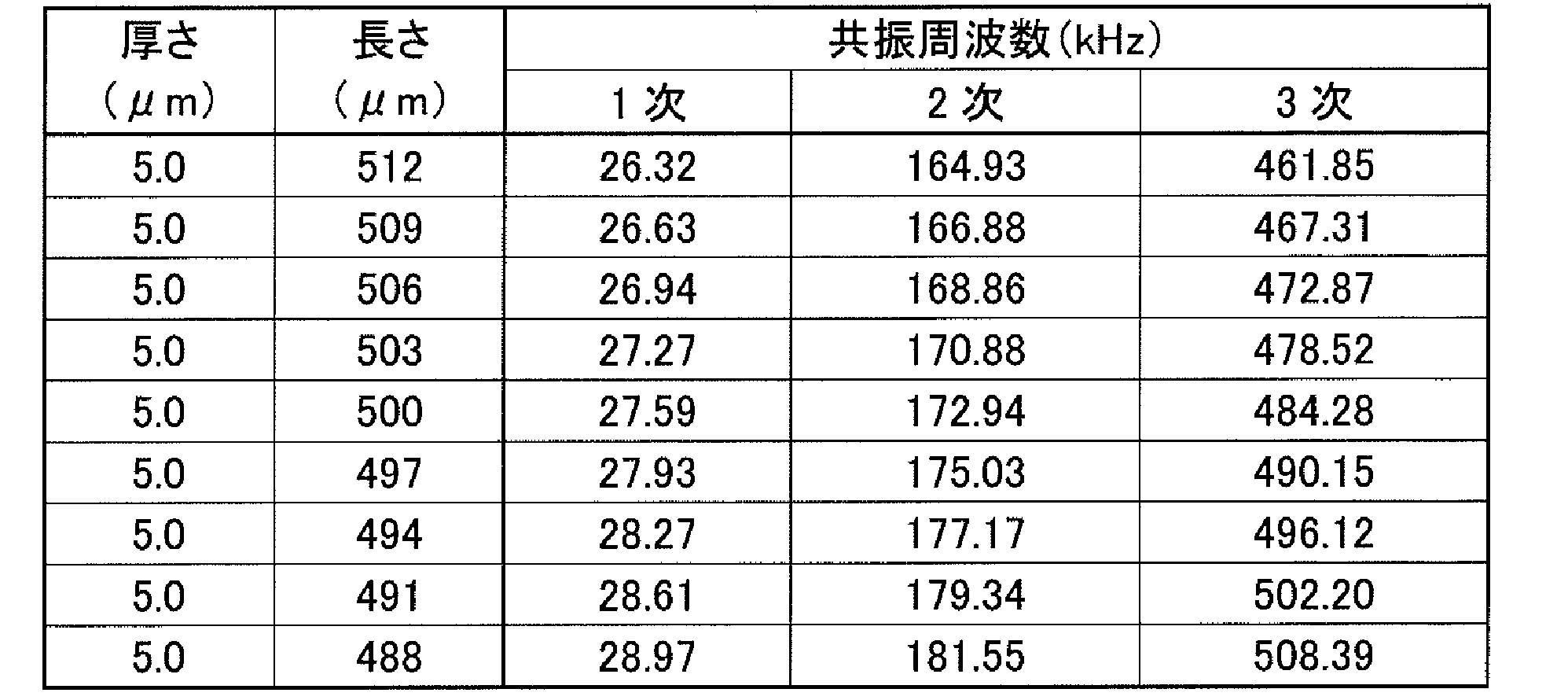
上記の計算結果から、3μm長さの違う振動子では、1次モードでは約0.3kHz、2次モードでは約2kHz、3次モードでは約6kHzづつ共振周波数がずれていることがわかる。一方で実際に製作した振動子(長さ500μm)のQ値測定から、振動の周波数応答における半値幅fHは、1次モードで0.13kHz、2次モードで0.30kHz、3次モードで0.53kHzであった。したがって、長さの違う振動子の共振周波数の差は設計通り、常に振動モードの半値幅よりも十分に大きく、振動ピークが分離できている。このような設計で作られた8個の振動子は、同一チップ内に置かれても互いに機械的・電気的に干渉することなく動作させることが可能となる。
実施例2は、図2に示した構成に対応したものであり、圧電層を各振動子上に配置したものを用いた。これ以外は、実施例1と同様である。
これにより各々の振動子は、互いに違う周波数で同時に振動させることができた。したがって、周波数の測定も同時に行うことができ、高速に並列検出が可能になる。
これにより各々の振動子は、互いに違う周波数で同時に振動させることができた。したがって、周波数の測定も同時に行うことができ、高速に並列検出が可能になる。
実施例3は、2個の振動子A、Bに異種の検出膜を塗布した例である。振動子A、Bの厚さは両者とも5μmであり、振動子Aは長さL=500μm、振動子Bは長さ500μm+ΔLとした。振動子Aには検出膜としてポリブタジエン(PBD)(密度ρ1=1.01g/cm3)を厚さt1=500nm塗布し、振動子Bには検出膜としてポリスチレン(PS)(密度ρ2=1.05g/cm3)を厚さt2=500nm塗布した。この振動子のQ値は1次モードで210であった。
また、比較のため、長さを振動子Aと同一の500μmとし、検出膜を振動子Bと同じポリスチレンとした振動子Cを作製した。
また、比較のため、長さを振動子Aと同一の500μmとし、検出膜を振動子Bと同じポリスチレンとした振動子Cを作製した。
このとき、式(5)および式(6)を使用して、1次の振動ピークが重ならない条件は
2(ΔL/L)>1/Q+(t2/t)×[1-(ρ2/ρ)]-(t1/t)×[1-(ρ1/ρ)] (7)
となる。これに数値を入れると、ΔL>0.98μmとなる。製造誤差を考え、ΔL=2μmとして式(4)より共振周波数を計算したところ、表2のようになった。
2(ΔL/L)>1/Q+(t2/t)×[1-(ρ2/ρ)]-(t1/t)×[1-(ρ1/ρ)] (7)
となる。これに数値を入れると、ΔL>0.98μmとなる。製造誤差を考え、ΔL=2μmとして式(4)より共振周波数を計算したところ、表2のようになった。
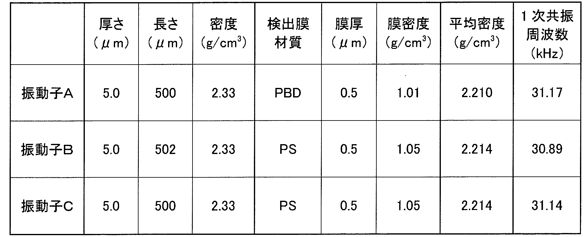
表2から、長さに2μmの差を与えた2つの振動子A、Bの共振周波数には0.28kHzの差が生じた。この値は1次モードの振動の周波数応答における半値幅fH=0.13kHzより大きくなり、式(7)の設計基準が妥当であることを示している。
一方で、振動子Bに対し、長さを振動子Aと同一とした振動子Cの場合は、検出膜の種類が異なる振動子Aとの共振周波数の差が0.03kHzと周波数応答の半値幅よりも狭くなり、互いに干渉すると考えられる。
以上のように、異種の検出膜を塗布した場合にも、長さに差を与えることで共振ピークが干渉しないように振動子を集積化することができる。
一方で、振動子Bに対し、長さを振動子Aと同一とした振動子Cの場合は、検出膜の種類が異なる振動子Aとの共振周波数の差が0.03kHzと周波数応答の半値幅よりも狭くなり、互いに干渉すると考えられる。
以上のように、異種の検出膜を塗布した場合にも、長さに差を与えることで共振ピークが干渉しないように振動子を集積化することができる。
なお、上記実施の形態において、圧電層43、44を設ける位置、範囲等は上記した以外のものとすることもできる。例えば、振動子30A、30B、…上に圧電層を設けても良い。この他、振動子30A、30B、…の駆動方式、振動変化の検出方式は、上記以外の方式を採用することもできる。
これ以外にも、本発明の主旨を逸脱しない限り、上記実施の形態で挙げた構成を取捨選択したり、他の構成に適宜変更することが可能である。
これ以外にも、本発明の主旨を逸脱しない限り、上記実施の形態で挙げた構成を取捨選択したり、他の構成に適宜変更することが可能である。
10…検出センサ、20…検出膜、30…振動子(振動子本体)、30A、30B…振動子、30a…固定端、40…駆動/検出部(駆動部、検出部)、42…周波数カウンタ、43…圧電層、44…圧電層、45…発振制御部、46…振動検出回路、47…発振回路、48…ピエゾ抵抗素子、49…マルチプレクサ、50…基板、51…キャビティ
Claims (9)
- 質量を有した物質の付着または吸着により振動特性が変化し、一端部が固定された梁状の複数の振動子と、
前記振動子を振動させる駆動部と、
前記振動子における振動の変化を検出することで、前記物質を検出する検出部と、を備え、
複数の前記振動子は互いに長さが異なり、任意の前記振動子を長さLとしたとき、長さLの前記振動子と他の前記振動子との長さの差ΔLが、
2(ΔL/L)>1/Q (ただし、Qは前記振動子のQ値)
となるよう設定され、
前記駆動部は、複数の前記振動子のそれぞれの共振周波数に応じた周波数で前記振動子を振動させることを特徴とする検出センサ。 - 前記駆動部は、
複数の前記振動子が設けられた基板の一面側に設けられた圧電層と、
前記圧電層に駆動電圧を印加する電極層と、
前記電極層に、前記駆動電圧として複数の前記振動子のいずれか一つの共振周波数に応じた周波数を有した電気的な信号を順次印加する発振制御部と、を備え、
前記検出部は、前記発振制御部で前記電極層に印加した電気的な信号の周波数に対応した共振周波数を有する前記振動子の振動の変化を検出することを特徴とする請求項1に記載の検出センサ。 - 前記駆動部は、
前記振動子のそれぞれの固定端近傍に設けられた圧電層と、
前記圧電層のそれぞれに駆動電圧を印加する電極層と、
前記電極層のそれぞれに設けられ、前気圧電層に電気的な信号を前記駆動電圧として印加する発振制御部と、を備え、
前記発振制御部は、前記電極層のそれぞれに、当該電極層に対応した前記振動子の共振周波数に応じた周波数を有した電気的な信号を印加することで、複数の前記振動子を同時に独立して振動させることを特徴とする請求項1に記載の検出センサ。 - 前記検出部は、前記振動子に付着した前記物質の量を検出することを特徴とする請求項1から3のいずれか一項に記載の検出センサ。
- 前記物質が特定の分子、あるいは特定の特性または特徴を有する複数種の分子であることを特徴とする請求項1から4のいずれか一項に記載の検出センサ。
- 前記振動子は、その表面に、二酸化チタン、ポリアクリル酸、ポリスチレン、ポリアクリルアミン、ポリジメチルシロキサン、ポリ塩化ビニル、ポリメタクリル酸メチル、ポリブタジエン、ポリスチレン重合体の少なくとも一つを含む材料からなる検出膜が形成されていることを特徴とする請求項1から5のいずれか一項に記載の検出センサ。
- 一端部が固定された梁状の複数の振動子本体と、
前記振動子本体のそれぞれの表面に設けられ、分子を吸着する検出膜と、を備え、
複数の前記振動子本体は互いに長さが異なり、任意の前記振動子を長さLとしたとき、長さLの前記振動子と他の前記振動子との長さの差ΔLが、
2(ΔL/L)>1/Q (ただし、Qは前記振動子のQ値)
となるよう設定されていることを特徴とする検出センサの振動子。 - 前記検出膜は、二酸化チタン、ポリアクリル酸、ポリスチレン、ポリアクリルアミン、ポリジメチルシロキサン、ポリ塩化ビニル、ポリメタクリル酸メチル、ポリブタジエン、ポリスチレン重合体の少なくとも一つを含んで形成されていることを特徴とする請求項7に記載の検出センサの振動子。
- 複数の前記振動子本体は、シリコン系材料からなる基板に形成されたキャビティに形成されていることを特徴とする請求項7または8に記載の検出センサの振動子。
Priority Applications (2)
| Application Number | Priority Date | Filing Date | Title |
|---|---|---|---|
| CN200980144356XA CN102209890B (zh) | 2008-11-07 | 2009-10-23 | 检测传感器、检测传感器的振子 |
| US13/096,409 US8258675B2 (en) | 2008-07-11 | 2011-04-28 | Detection sensor and resonator of detection sensor |
Applications Claiming Priority (2)
| Application Number | Priority Date | Filing Date | Title |
|---|---|---|---|
| JP2008287018A JP5130422B2 (ja) | 2008-11-07 | 2008-11-07 | 検出センサ |
| JP2008-287018 | 2008-11-07 |
Related Child Applications (1)
| Application Number | Title | Priority Date | Filing Date |
|---|---|---|---|
| US13/096,409 Continuation US8258675B2 (en) | 2008-07-11 | 2011-04-28 | Detection sensor and resonator of detection sensor |
Publications (1)
| Publication Number | Publication Date |
|---|---|
| WO2010052841A1 true WO2010052841A1 (ja) | 2010-05-14 |
Family
ID=42152654
Family Applications (1)
| Application Number | Title | Priority Date | Filing Date |
|---|---|---|---|
| PCT/JP2009/005587 Ceased WO2010052841A1 (ja) | 2008-07-11 | 2009-10-23 | 検出センサ、検出センサの振動子 |
Country Status (4)
| Country | Link |
|---|---|
| US (1) | US8258675B2 (ja) |
| JP (1) | JP5130422B2 (ja) |
| CN (1) | CN102209890B (ja) |
| WO (1) | WO2010052841A1 (ja) |
Families Citing this family (18)
| Publication number | Priority date | Publication date | Assignee | Title |
|---|---|---|---|---|
| JP5242347B2 (ja) * | 2008-11-11 | 2013-07-24 | 独立行政法人産業技術総合研究所 | 検出センサ |
| US9939412B2 (en) | 2013-02-06 | 2018-04-10 | Empire Technology Development Llc | Devices, systems, and methods for detecting odorants |
| JP2014190771A (ja) * | 2013-03-26 | 2014-10-06 | National Institute Of Advanced Industrial & Technology | 質量測定方法及び質量測定装置 |
| WO2014171927A1 (en) * | 2013-04-16 | 2014-10-23 | Empire Technology Development Llc | Graded structure films |
| US9702846B2 (en) | 2013-11-08 | 2017-07-11 | Taiwan Semiconductor Manufacturing Company, Ltd. | Biosensor device and related method |
| WO2015116102A1 (en) * | 2014-01-30 | 2015-08-06 | Empire Technology Development Llc | Odor sensors |
| US20170040971A1 (en) * | 2014-01-30 | 2017-02-09 | Empire Technology Development Llc | Crystal oscillators and methods for fabricating the same |
| CN105067471B (zh) * | 2015-07-24 | 2017-12-29 | 中国科学院上海微系统与信息技术研究所 | 一种微悬臂谐振结构传感器及其制造方法 |
| JP6764281B2 (ja) | 2016-08-09 | 2020-09-30 | 太陽誘電株式会社 | ガスセンサ |
| JP6863009B2 (ja) * | 2017-03-31 | 2021-04-21 | I−Pex株式会社 | 物質検出素子 |
| US20220011209A1 (en) * | 2018-12-12 | 2022-01-13 | Micro Motion, Inc. | Planar vibratory densitometer, densitometer member, and related method |
| KR102739123B1 (ko) * | 2018-12-28 | 2024-12-06 | 삼성전자주식회사 | 공진기 및 그 제조방법과, 공진기를 포함하는 스트레인 센서 및 센서 어레이 |
| US20210041287A1 (en) | 2019-08-09 | 2021-02-11 | Apple Inc. | On-Bed Differential Piezoelectric Sensor |
| US11896136B2 (en) | 2019-09-19 | 2024-02-13 | Apple Inc. | Pneumatic haptic device having actuation cells for producing a haptic output over a bed mattress |
| US20210255082A1 (en) * | 2020-02-19 | 2021-08-19 | Tdk Corporation | Methods and Devices for Detecting Particles Using a Cantilever Sensor |
| US11771406B2 (en) | 2020-08-12 | 2023-10-03 | Apple Inc. | In-bed temperature array for menstrual cycle tracking |
| US12582332B2 (en) | 2021-06-23 | 2026-03-24 | Apple Inc. | Piezoelectric sensor with resonating microstructures |
| US11874189B2 (en) * | 2021-07-02 | 2024-01-16 | Applied Materials, Inc. | MEMS resonator sensor substrate for plasma, temperature, stress, or deposition sensing |
Citations (3)
| Publication number | Priority date | Publication date | Assignee | Title |
|---|---|---|---|---|
| WO2004061427A1 (ja) * | 2002-12-27 | 2004-07-22 | Japan Science And Technology Agency | マルチカンチレバーの振動周波数の計測方法及び装置 |
| WO2008069247A1 (ja) * | 2006-12-05 | 2008-06-12 | National University Corporation Gunma University | 質量測定装置及びカンチレバ |
| JP2008241619A (ja) * | 2007-03-28 | 2008-10-09 | Gunma Univ | カンチレバー、バイオセンサ、及びプローブ顕微鏡 |
Family Cites Families (10)
| Publication number | Priority date | Publication date | Assignee | Title |
|---|---|---|---|---|
| US5162691A (en) * | 1991-01-22 | 1992-11-10 | The United States Of America As Represented By The Secretary Of The Army | Cantilevered air-gap type thin film piezoelectric resonator |
| US5856722A (en) * | 1996-01-02 | 1999-01-05 | Cornell Research Foundation, Inc. | Microelectromechanics-based frequency signature sensor |
| JP3348687B2 (ja) * | 1998-05-22 | 2002-11-20 | 住友金属工業株式会社 | 振動波検出方法及び装置 |
| AU737757B2 (en) * | 1998-11-02 | 2001-08-30 | Kabushiki Kaisha Meidensha | QCM sensor |
| US7369115B2 (en) * | 2002-04-25 | 2008-05-06 | Immersion Corporation | Haptic devices having multiple operational modes including at least one resonant mode |
| WO2004023108A1 (ja) * | 2002-09-05 | 2004-03-18 | Tokyo University Of Pharmacy And Life Science | 水晶振動子型ナノチャンネルセンサー |
| JP2007240252A (ja) | 2006-03-07 | 2007-09-20 | National Institute Of Advanced Industrial & Technology | 検出センサ、振動子 |
| WO2008126519A1 (ja) * | 2007-03-22 | 2008-10-23 | Shinshu University | センサー |
| KR100975010B1 (ko) * | 2008-02-29 | 2010-08-09 | 성균관대학교산학협력단 | 다중 크기 압전 마이크로 칸티레버 공진자 어레이를 이용한 물리센서 및 그 제작방법 |
| US8199389B2 (en) * | 2008-03-10 | 2012-06-12 | Ricoh Company, Ltd. | Vibration elements |
-
2008
- 2008-11-07 JP JP2008287018A patent/JP5130422B2/ja not_active Expired - Fee Related
-
2009
- 2009-10-23 CN CN200980144356XA patent/CN102209890B/zh not_active Expired - Fee Related
- 2009-10-23 WO PCT/JP2009/005587 patent/WO2010052841A1/ja not_active Ceased
-
2011
- 2011-04-28 US US13/096,409 patent/US8258675B2/en not_active Expired - Fee Related
Patent Citations (3)
| Publication number | Priority date | Publication date | Assignee | Title |
|---|---|---|---|---|
| WO2004061427A1 (ja) * | 2002-12-27 | 2004-07-22 | Japan Science And Technology Agency | マルチカンチレバーの振動周波数の計測方法及び装置 |
| WO2008069247A1 (ja) * | 2006-12-05 | 2008-06-12 | National University Corporation Gunma University | 質量測定装置及びカンチレバ |
| JP2008241619A (ja) * | 2007-03-28 | 2008-10-09 | Gunma Univ | カンチレバー、バイオセンサ、及びプローブ顕微鏡 |
Also Published As
| Publication number | Publication date |
|---|---|
| JP5130422B2 (ja) | 2013-01-30 |
| CN102209890B (zh) | 2013-02-20 |
| JP2010112888A (ja) | 2010-05-20 |
| US20110266919A1 (en) | 2011-11-03 |
| US8258675B2 (en) | 2012-09-04 |
| CN102209890A (zh) | 2011-10-05 |
Similar Documents
| Publication | Publication Date | Title |
|---|---|---|
| JP5130422B2 (ja) | 検出センサ | |
| JP5242347B2 (ja) | 検出センサ | |
| JP5019120B2 (ja) | 検出センサ | |
| US7812692B2 (en) | Piezo-on-diamond resonators and resonator systems | |
| Suzuki et al. | A silicon electrostatic ultrasonic transducer | |
| US6797631B2 (en) | High sensitive micro-cantilever sensor and fabricating method thereof | |
| US8136403B2 (en) | Micromechanical sensor, sensor array and method | |
| EP3605057B1 (en) | Substance detecting element | |
| US9465012B2 (en) | Measurement method using a sensor; sensor system and sensor | |
| US9134276B2 (en) | Bulk acoustic wave resonator sensor | |
| JP5083984B2 (ja) | 検出センサ、振動子 | |
| EP2176949A2 (en) | Saw sensor | |
| Ferrari et al. | Development and application of mass sensors based on flexural resonances in alumina beams | |
| JP3908713B2 (ja) | 原子間力顕微鏡用力方位センサ付カンチレバー | |
| Herth et al. | Modeling and detecting response of micromachining square and circular membranes transducers based on AlN thin film piezoelectric layer | |
| JP2009133772A (ja) | 検出センサ、振動子 | |
| US7716986B2 (en) | Acoustic wave sensing device integrated with micro-channels and method for the same | |
| US7467553B2 (en) | Capacitively coupled resonator drive | |
| Alava et al. | Silicon-based micromembranes with piezoelectric actuation and piezoresistive detection for sensing purposes in liquid media | |
| Isarakorn et al. | Finite element analysis and experiments on a silicon membrane actuated by an epitaxial PZT thin film for localized-mass sensing applications | |
| Park | Capacitive micromachined ultrasonic transducer (CMUT) for chemical detection in air | |
| US20250317117A1 (en) | Self-referencing microelectromechanical systems (mems) resonator with dual mechanical modes for temperature-independent environmental sensing | |
| Pachkawade | NEMS based actuation and sensing | |
| Zhao et al. | Lateral-Field-Excited PMUTs Based on Bilayer X-Cut Lithium Niobate | |
| Johnston | Thin-film bulk acoustic resonators on integrated circuits for physical sensing applications |
Legal Events
| Date | Code | Title | Description |
|---|---|---|---|
| WWE | Wipo information: entry into national phase |
Ref document number: 200980144356.X Country of ref document: CN |
|
| 121 | Ep: the epo has been informed by wipo that ep was designated in this application |
Ref document number: 09824542 Country of ref document: EP Kind code of ref document: A1 |
|
| NENP | Non-entry into the national phase |
Ref country code: DE |
|
| 122 | Ep: pct application non-entry in european phase |
Ref document number: 09824542 Country of ref document: EP Kind code of ref document: A1 |