WO2010050120A1 - シリコンウェーハの製造方法 - Google Patents
シリコンウェーハの製造方法 Download PDFInfo
- Publication number
- WO2010050120A1 WO2010050120A1 PCT/JP2009/004955 JP2009004955W WO2010050120A1 WO 2010050120 A1 WO2010050120 A1 WO 2010050120A1 JP 2009004955 W JP2009004955 W JP 2009004955W WO 2010050120 A1 WO2010050120 A1 WO 2010050120A1
- Authority
- WO
- WIPO (PCT)
- Prior art keywords
- silicon wafer
- heat treatment
- ppm
- gas
- nitrogen gas
- Prior art date
- Legal status (The legal status is an assumption and is not a legal conclusion. Google has not performed a legal analysis and makes no representation as to the accuracy of the status listed.)
- Ceased
Links
Images


Classifications
-
- H—ELECTRICITY
- H10—SEMICONDUCTOR DEVICES; ELECTRIC SOLID-STATE DEVICES NOT OTHERWISE PROVIDED FOR
- H10P—GENERIC PROCESSES OR APPARATUS FOR THE MANUFACTURE OR TREATMENT OF DEVICES COVERED BY CLASS H10
- H10P36/00—Gettering within semiconductor bodies
- H10P36/20—Intrinsic gettering, i.e. thermally inducing defects by using oxygen present in the silicon body
Definitions
- the present invention relates to a method for manufacturing a silicon wafer in which holes are formed in a bulk portion by RTA heat treatment and gettering capability is imparted.
- a silicon wafer manufactured by processing a silicon single crystal pulled and grown by the CZ (Czochralski) method contains a large amount of oxygen impurities, and these oxygen impurities cause oxygen precipitates (dislocations, defects, etc.).
- BMD Bulk Micro Defect
- RTA Rapid Thermal Annealing
- a vacancy (hereinafter simply referred to as a vacancy) is formed, frozen by rapid cooling, and a DZ layer (denuded zone or defect-free layer) is formed by outward diffusion of vacancies on the surface by subsequent heat treatment.
- a uniform forming method is used (see Patent Document 1).
- the silicon wafer thus obtained has a DZ layer 31 in the surface layer and a BMD layer 32 in the bulk part as shown in FIG.
- N 2 nitrogen
- Si x N y nitride film
- Patent Document 2 an atmosphere gas in a heat treatment process in which a silicon wafer is heat-treated to newly form vacancies therein is used as a nitriding gas (NH 3 or the like) having a decomposition temperature lower than a temperature at which N 2 can be decomposed. Proposed to contain atmospheric gas.
- the nitriding gas is decomposed even at a lower heat treatment temperature or shorter heat treatment time than in the case of N 2 , so that the silicon wafer surface can be nitrided and vacancies can be injected into the inside, thereby suppressing the occurrence of slip during heat treatment.
- a high-quality wafer having a sufficient DZ layer on the surface and a moderately high BMD density in the bulk portion can be obtained by subsequent heat treatment.
- the present invention has been made in view of such problems, and it is possible to reduce the temperature or shorten the time of the RTA heat treatment applied to the silicon wafer, to suppress the occurrence of slip of the silicon wafer, and to use NH 3 . It is an object of the present invention to provide a method capable of manufacturing a high-quality silicon wafer by injecting holes into the silicon wafer without performing the above process.
- the present invention is a method for producing a silicon wafer having at least a step of subjecting a silicon wafer to RTA heat treatment in an atmospheric gas, wherein the atmospheric gas contains 5 ppm or more and 250 ppm or less in nitrogen gas.
- a method for producing a silicon wafer characterized in that an RTA heat treatment is performed using a mixture of moisture at a concentration.
- a slip-free high-quality silicon wafer having a DZ layer on the surface layer and a BMD having a sufficient density in the bulk portion can be manufactured at a low cost by the subsequent heat treatment.
- a nitrogen gas mixed with moisture having a concentration of 10 ppm or more and 150 ppm or less as the atmospheric gas.
- a gas mixed with nitrogen gas with a concentration of 10 ppm or more and 150 ppm or less as an atmospheric gas more vacancies can be injected into the wafer.
- a BMD density equal to or higher than that obtained when the RTA heat treatment is performed in an atmosphere using NH 3 can be obtained.
- the concentration of moisture mixed into the nitrogen gas by controlling the dew point of the nitrogen gas as the atmospheric gas. In this way, by controlling the dew point of nitrogen gas, it is possible to more easily adjust the moisture concentration to be mixed.
- the initial oxygen concentration of the silicon wafer subjected to the RTA heat treatment is 9 ppma or more and 14 ppma or less. Even with such a low oxygen concentration silicon wafer, if the RTA heat treatment of the present invention is used, a sufficient amount of vacancies can be injected even at a low temperature, and a silicon wafer having a high BMD density without slipping can be obtained. Therefore, it is preferable without excessive precipitation.
- an epitaxial layer can be grown on the surface of the silicon wafer subjected to the RTA heat treatment.
- a silicon wafer subjected to the RTA heat treatment of the present invention has a sufficient amount of vacancies in the bulk portion and has good surface crystallinity. Since favorable oxygen precipitation occurs, it can have a high BMD density, and a good epitaxial layer can be obtained, it is preferable.
- a silicon wafer having no DZ layer and a high BMD density can be produced at low cost without using a toxic gas such as NH 3 or the like.
- FIG. 1 is a graph showing the relationship between the BMD density and the moisture concentration mixed in nitrogen gas as the atmosphere gas for the RTA heat treatment.
- the BMD density is significantly lowered. This is because an oxide film is formed by water during the RTA heat treatment, and interstitial Si is injected to reduce the amount of vacancies. This is considered to be because oxygen precipitation is suppressed.
- the present invention has been completed by finding that a silicon wafer having a high density of BMD layers can be manufactured by performing a simple hole injection.
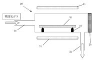
- FIG. 2 shows an example of a heat treatment furnace for RTA that can be used in the present invention.
- a heat treatment furnace substantially the same as the conventional one can be used.
- the heat treatment furnace 20 is provided with a lid 25 for closing the carry-in port of the silicon wafer W, a gas supply port 22 for supplying atmospheric gas, a gas discharge port 24 for discharging atmospheric gas, and a silicon wafer W.
- the susceptor 23 and the lamp 21 for heating the silicon wafer W are provided.
- the silicon wafer W is placed in such a heat treatment furnace 20 and the RTA heat treatment is performed while flowing the atmospheric gas from the gas supply port 22.
- an atmosphere gas in the RTA heat treatment using the heat treatment furnace as described above is a nitrogen gas mixed with moisture having a concentration of 5 ppm or more and 250 ppm or less.
- Ordinary pure nitrogen gas has at least a moisture content of about 2 ppm or less. Conventionally, it has been assumed that vacancy injection occurs in an atmosphere that does not contain moisture, so the moisture concentration of the pure nitrogen gas is even smaller. It was adjusted to be.
- an oxynitride film is formed on the surface of a silicon wafer even by a relatively low temperature heat treatment by performing an RTA heat treatment in an atmosphere in which a minute amount of moisture within the range of the present invention is intentionally mixed in nitrogen gas. Can be formed. As a result, the reaction between nitrogen and silicon atoms enables efficient injection of holes into the silicon wafer.
- a sufficient amount of vacancies can be injected into the silicon wafer by heat treatment at a relatively low temperature without using a toxic gas such as NH 3 as the atmospheric gas.
- a toxic gas such as NH 3 as the atmospheric gas.
- the water concentration mixed in nitrogen gas shall be 10 ppm or more and 150 ppm or less.
- the water concentration mixed in nitrogen gas shall be 10 ppm or more and 150 ppm or less.
- the moisture concentration mixed into the nitrogen gas by controlling the dew point of the nitrogen gas.
- the nitrogen gas has a concentration of 10 ppm or higher.
- Table 1 The relationship between the dew point of nitrogen gas and the water concentration is shown in Table 1.
- the dew point may be controlled to be ⁇ 65 ° C. or more and ⁇ 34 ° C. or less. It can be seen that the nitrogen gas dew point should be controlled to -60 ° C. or higher and ⁇ 38 ° C. or lower in order to adjust the range (10 ppm or more and 150 ppm or less).
- the silicon wafer subjected to the RTA heat treatment of the present invention is not particularly limited, but for example, a silicon wafer having an initial oxygen concentration of 9 ppma to 14 ppma (JEIDA) is preferable. Even with such a relatively low oxygen concentration silicon wafer, if the RTA heat treatment of the present invention is used, a sufficient amount of vacancies can be injected even at a low temperature, and a silicon wafer having a high BMD density without slipping can be obtained. It can be manufactured and is suitable without causing excessive precipitation.
- JEIDA initial oxygen concentration
- the conditions for the RTA heat treatment of the present invention are not particularly limited.
- the temperature is raised at 20 to 50 ° C./sec, and after heat treatment at 1100 ° C. to 1200 ° C. for 60 seconds or less, 20 The temperature can be lowered at -50 ° C / sec.
- the RTA heat treatment according to the present invention can inject holes even at a relatively low temperature such as 1100 to 1200 ° C. Therefore, the silicon wafer can be satisfactorily heat-treated without slipping.
- the heat treatment time can be set to less than 10 seconds, and sufficient vacancies can be injected even in a short time. It is also possible to freeze more holes by increasing the temperature drop rate.
- the silicon wafer subjected to the RTA heat treatment of the present invention since the silicon wafer subjected to the RTA heat treatment of the present invention has no slip and has a sufficient amount of pores, 5 ⁇ 10 8 / cm 3 or more is obtained by heat treatment for precipitating oxygen in the subsequent step. Furthermore, it becomes a high-quality silicon wafer having a sufficiently high BMD density of 2 ⁇ 10 9 / cm 3 or more in the bulk part and having a DZ layer on the surface.
- the silicon wafer subjected to the RTA heat treatment of the present invention has a sufficient amount of vacancies, good oxygen precipitation occurs in the production of a silicon wafer epitaxially grown at a high temperature, and a high BMD density. It is possible to make an epitaxial wafer having
- a silicon wafer having an initial oxygen concentration of 12 ppma (JEIDA) was prepared as a silicon wafer to be heat-treated.
- the atmosphere gas was prepared by changing the moisture concentration to be mixed into the nitrogen gas in the range of 0 ppm to 300 ppm, with an RTA heat treatment temperature of 1175 ° C., a heat treatment time of 30 seconds, a heating rate of 50 ° C./sec, and a cooling rate of 33 ° C./sec.
- the silicon wafer was subjected to RTA heat treatment. Further, the silicon wafer was subjected to heat treatment under the same conditions except that a mixed gas of NH 3 and Ar was used as the atmospheric gas.
- the silicon wafer subjected to the RTA heat treatment as described above was subjected to a two-step heat treatment (800 ° C./4 hours, 1000 ° C./16 hours) for BMD evaluation.
- the silicon wafer after the two-stage heat treatment was cleaved and etched to observe the BMD layer from the surface layer to 500 ⁇ m, and the BMD density was measured.
- FIG. 4 is a diagram observing the BMD layer.
- FIG. 1 and Table 2 show the BMD density measurement results.
- an oxynitride film or a nitride film was formed on the silicon wafer surface in both the example (N 2 + H 2 O (5 to 250 ppm)) and the comparative example (NH 3 / Ar).
- the film thickness was thin compared to the comparative example.
- the BMD density was higher in the example than in the comparative example. This is because the larger the amount of holes injected, the smaller the size of the BMD, and the smaller BMD tends to disappear in the subsequent heat treatment step. Therefore, the example has more appropriate holes than the comparative example (NH 3 / Ar). It turns out that it was the injection amount. For this reason, it can be seen that the silicon wafer subjected to the RTA heat treatment of the present invention is suitable for a wafer for epitaxial layer growth that requires high-temperature heat treatment.
- the present invention is not limited to the above embodiment.
- the above embodiment is merely an example, and the present invention has the same configuration as that of the technical idea described in the claims of the present invention, and any device that exhibits the same function and effect is the present invention. It is included in the technical scope of the invention.
Landscapes
- Crystals, And After-Treatments Of Crystals (AREA)
Abstract
本発明は、雰囲気ガス中でシリコンウェーハにRTA熱処理を施す工程を有するシリコンウェーハの製造方法であって、雰囲気ガスとして、窒素ガスに5ppm以上250ppm以下の濃度の水分を混入させたものを用いてRTA熱処理を施すシリコンウェーハの製造方法である。これにより、シリコンウェーハに施すRTA熱処理の低温化又は短時間化を図り、シリコンウェーハのスリップの発生を抑制すると共に、NH3を使用することなく、シリコンウェーハ内部に空孔を形成し、高品質なシリコンウェーハを製造することができる方法が提供される。
Description
本発明は、RTA熱処理によりバルク部に空孔を形成し、ゲッタリング能力を付与するシリコンウェーハの製造方法に関する。
CZ(チョクラルスキー)法で引上成長されたシリコン単結晶を加工して製作されたシリコンウェーハは、酸素不純物を多く含んでおり、この酸素不純物は転位や欠陥等を生じさせる酸素析出物(BMD:Bulk Micro Defect)となる。酸素析出物はデバイスが形成される表面にある場合、リーク電流増大や酸化膜耐圧低下等の原因になって半導体デバイスの特性に大きな影響を及ぼす。
このため、従来、シリコンウェーハ表面に対し、1250℃以上の高温で短時間の急速加熱・急冷の熱処理(RTA:Rapid Thermal Annealing)を所定の雰囲気ガス中で施し、内部に高濃度の熱平衡の原子空孔(Vacancy:以下、単に空孔と称す)を形成し、急冷により凍結すると共に、この後の熱処理で表面において空孔を外方拡散させることによりDZ層(Denuded Zone又は無欠陥層)を均一に形成する方法が用いられている(特許文献1参照)。そして、このDZ層形成後に、上記熱処理温度より低温で熱処理を施すことで、バルク部の欠陥層として酸素析出核を形成・安定化してゲッタリング効果を有するBMD層を形成する工程が採用されている。このようにして得られるシリコンウェーハは、図3のように表層にDZ層31、バルク部にBMD層32を有する。
また、他の方法として、先ず酸素雰囲気下で熱処理を行い、続けて非酸化性雰囲気下で熱処理を行うことにより、シリコンウェーハ表面にDZ層、バルク部にBMD層の形成を行っている。なお、従来、空孔形成のための熱処理においては、雰囲気ガスとしてN2(窒素)が主に用いられている。すなわち、高温で窒素が分解され、シリコンウェーハ表面にSixNy(窒化膜)が形成されることにより、空孔を注入するものである。
しかしながら、上記のようなシリコンウェーハの熱処理技術では、以下のような課題が残されている。従来では、空孔形成のための熱処理を施す際に、窒素を主とした雰囲気ガス中で熱処理が行われるが、この場合、十分な量の空孔を得るために1250℃以上かつ10sec以上の熱処理が必要であった。
このため、シリコンウェーハには、高温の熱処理により、サセプタ又は支持ピン等と接触する部分からスリップが発生してしまい、割れ等の原因になる不都合があった。
このため、シリコンウェーハには、高温の熱処理により、サセプタ又は支持ピン等と接触する部分からスリップが発生してしまい、割れ等の原因になる不都合があった。
そこで、特許文献2では、シリコンウェーハを熱処理して内部に新たに空孔を形成する熱処理工程の雰囲気ガスを、N2が分解可能な温度よりも低い分解温度の窒化ガス(NH3等)を含む雰囲気ガスとすることを提案している。これにより、N2の場合よりも低い熱処理温度又は短い熱処理時間でも窒化ガスが分解されてシリコンウェーハ表面を窒化し、内部に空孔を注入することができ、熱処理時のスリップ発生を抑制することができると共に、その後の熱処理で表面に十分なDZ層とバルク部に適度に高いBMD密度を有した高品質なウェーハを得ることができるとしている。
しかしながら、有害なNH3を供給するための設備が必要となり、設備コストが増大してしまうという問題があった。
そこで、本発明は、このような問題点に鑑みてなされたもので、シリコンウェーハに施すRTA熱処理の低温化又は短時間化を図り、シリコンウェーハのスリップの発生を抑制すると共に、NH3を使用することなく、シリコンウェーハ内部に空孔を注入し、高品質なシリコンウェーハを製造することができる方法を提供することを目的とする。
上記目的を達成するために、本発明は、少なくとも、雰囲気ガス中でシリコンウェーハにRTA熱処理を施す工程を有するシリコンウェーハの製造方法であって、前記雰囲気ガスとして、窒素ガスに5ppm以上250ppm以下の濃度の水分を混入させたものを用いてRTA熱処理を施すことを特徴とするシリコンウェーハの製造方法を提供する。
このように、窒素ガスに微量の水分を混入させた雰囲気中でRTA熱処理を行うことにより、比較的低温の熱処理でもシリコンウェーハ表面に酸窒化膜を形成することができる。このため、窒素とシリコン原子が反応することで、シリコンウェーハ内部に効率的に空孔を注入することができる。これにより雰囲気ガスにNH3等の有毒ガスを用いなくとも、比較的低温の熱処理で、シリコンウェーハ内部に十分な量の空孔を注入することができる。
従って、本発明のRTA熱処理を行うことで、その後の熱処理により表層にDZ層と、バルク部に十分な密度のBMDを有したスリップのない高品質なシリコンウェーハを低コストで製造することができる。
従って、本発明のRTA熱処理を行うことで、その後の熱処理により表層にDZ層と、バルク部に十分な密度のBMDを有したスリップのない高品質なシリコンウェーハを低コストで製造することができる。
このとき、前記雰囲気ガスとして、窒素ガスに10ppm以上150ppm以下の濃度の水分を混入させたものを用いることが好ましい。
このように、窒素ガスに10ppm以上150ppm以下の濃度の水分を混入させたものを雰囲気ガスとして用いることで、より多くの空孔をウェーハ内部に注入することができ、低温熱処理であっても、NH3を用いた雰囲気でRTA熱処理を行った場合と同等以上のBMD密度を得ることができる。
このように、窒素ガスに10ppm以上150ppm以下の濃度の水分を混入させたものを雰囲気ガスとして用いることで、より多くの空孔をウェーハ内部に注入することができ、低温熱処理であっても、NH3を用いた雰囲気でRTA熱処理を行った場合と同等以上のBMD密度を得ることができる。
このとき、前記雰囲気ガスとして、窒素ガスの露点を制御することにより窒素ガスに混入させる水分の濃度を調整することが好ましい。
このように、窒素ガスの露点を制御することで、混入させる水分濃度の調整をより容易に行うことができる。
このように、窒素ガスの露点を制御することで、混入させる水分濃度の調整をより容易に行うことができる。
このとき、前記雰囲気ガスとして、窒素ガスの露点を-60℃以上-38℃以下に制御することにより、窒素ガスに10ppm以上150ppm以下の濃度の水分を混入させることが好ましい。
窒素ガスの露点を上記範囲に制御することで、10ppm以上150ppm以下という好ましい水分濃度範囲内により容易に調整することができる。
窒素ガスの露点を上記範囲に制御することで、10ppm以上150ppm以下という好ましい水分濃度範囲内により容易に調整することができる。
このとき、前記RTA熱処理が施されるシリコンウェーハの初期酸素濃度を、9ppma以上14ppma以下とすることが好ましい。
このような、低酸素濃度のシリコンウェーハであっても本発明のRTA熱処理であれば、低温でも十分な空孔量を注入することができ、スリップがなく、高いBMD密度のシリコンウェーハにすることができるため、析出過多になることもなく好適である。
このような、低酸素濃度のシリコンウェーハであっても本発明のRTA熱処理であれば、低温でも十分な空孔量を注入することができ、スリップがなく、高いBMD密度のシリコンウェーハにすることができるため、析出過多になることもなく好適である。
このとき、前記RTA熱処理が施されたシリコンウェーハの表面に、エピタキシャル層を成長させることができる。
本発明のRTA熱処理が施されたシリコンウェーハであれば、バルク部に十分な量の空孔を有しており、表面の結晶性も良好であるので高温でエピタキシャル成長を行うシリコンウェーハの製造においても、良好な酸素析出が起こり、高いBMD密度を有することができるとともに、良好なエピタキシャル層を得ることができるので、好適である。
本発明のRTA熱処理が施されたシリコンウェーハであれば、バルク部に十分な量の空孔を有しており、表面の結晶性も良好であるので高温でエピタキシャル成長を行うシリコンウェーハの製造においても、良好な酸素析出が起こり、高いBMD密度を有することができるとともに、良好なエピタキシャル層を得ることができるので、好適である。
本発明であれば、NH3等の有毒ガスを使用せずに、スリップがなく、DZ層と高いBMD密度を有するシリコンウェーハを低コストで製造することができる。
従来、NH3等の有毒なガスを用いるか、又は高温の熱処理を行ってシリコンウェーハに空孔を注入していたが、スリップの発生やコストの問題等があった。
これに対して、本発明者らは、比較的低温の熱処理であっても、NH3等を用いること無く空孔を注入できる熱処理方法を鋭意検討した結果、RTA熱処理の際の雰囲気として、窒素ガスに微量の水分を混入させたものを用いることで、比較的低温であってもシリコンウェーハ内部へ空孔が注入されることを見出した。
これに対して、本発明者らは、比較的低温の熱処理であっても、NH3等を用いること無く空孔を注入できる熱処理方法を鋭意検討した結果、RTA熱処理の際の雰囲気として、窒素ガスに微量の水分を混入させたものを用いることで、比較的低温であってもシリコンウェーハ内部へ空孔が注入されることを見出した。
さらに、本発明者らは、適切な水分量を調べるために、様々な水分濃度の窒素ガス雰囲気と、NH3を含む雰囲気によりRTA熱処理(1175℃/30秒)を行ったシリコンウェーハに、酸素析出物であるBMDを形成するための2段階熱処理(800℃/4時間、1000℃/16時間)を施して、そのBMD密度を調べることにより、図1のような結果を得た。図1は、RTA熱処理の雰囲気ガスとして窒素ガスに混入させた水分濃度と、BMD密度の関係を示すグラフである。
図1からわかるように、RTA熱処理温度が比較的低温であるため純粋な窒素ガス(N2)では酸素析出は不十分であるが、窒素ガスに水分を5ppm(N2+H2O(5ppm))以上混入させることで酸素析出が良好に生じており、さらには、10ppm~150ppmの範囲では、同様の熱処理条件でNH3を含む雰囲気ガス(NH3/Ar)中でRTA熱処理を行ったものよりもBMD密度が高いことがわかる。
また、水分濃度が250ppmを超えると大幅にBMD密度が低くなっているが、これは、RTA熱処理中に水分により酸化膜が形成されてしまい、格子間Siが注入されて空孔量が減少して酸素析出が抑制されてしまうためと考えられる。
以上から、RTA熱処理の雰囲気ガスとして、窒素ガスに5ppm以上250ppm以下の濃度の水分、好ましくは10ppm以上150ppm以下の濃度の水分を混入させたものを用いることで、比較的低温であっても十分な空孔注入ができ、高密度のBMD層を有するシリコンウェーハを製造できることを見出して、本発明を完成させた。
以下、図を参照しながら、本発明の実施の形態について具体的に説明するが、本発明はこれらに限定されるものではない。
先ず、図2に本発明で使用することができるRTA用の熱処理炉の一例を示す。本発明ではNH3等の有毒ガスを用いる必要が無いため、熱処理炉としては、実質的に従来のものと同様のものを使用できる。
熱処理炉20は、シリコンウェーハWの搬入口をふさぐための蓋25、雰囲気ガスを供給するためのガス供給口22、雰囲気ガスを排出するためのガス排出口24、シリコンウェーハWを載置するためのサセプタ23とシリコンウェーハWを加熱するランプ21を具備している。
このような熱処理炉20内にシリコンウェーハWを載置して、ガス供給口22から雰囲気ガスを流しながら、RTA熱処理を行う。
熱処理炉20は、シリコンウェーハWの搬入口をふさぐための蓋25、雰囲気ガスを供給するためのガス供給口22、雰囲気ガスを排出するためのガス排出口24、シリコンウェーハWを載置するためのサセプタ23とシリコンウェーハWを加熱するランプ21を具備している。
このような熱処理炉20内にシリコンウェーハWを載置して、ガス供給口22から雰囲気ガスを流しながら、RTA熱処理を行う。
本発明では、上記のような熱処理炉を用いたRTA熱処理における雰囲気ガスとして、窒素ガスに5ppm以上250ppm以下の濃度の水分を混入させたものを用いる。
通常の純粋な窒素ガスは、少なくとも水分を2ppm以下程度にされており、従来では水分を含まない雰囲気の方が空孔注入が起きるとされていたため、その純粋な窒素ガスの水分濃度はさらに小さくなるように調整されていた。
これに対して本発明では、窒素ガスに本発明の範囲の微量濃度の水分を故意に混入させた雰囲気中でRTA熱処理を行うことにより、比較的低温の熱処理でもシリコンウェーハ表面に酸窒化膜を形成することができる。これにより、窒素とシリコン原子が反応することで、シリコンウェーハ内部に効率的に空孔を注入することができる。このため、雰囲気ガスにNH3等の有毒ガスを用いなくとも、比較的低温の熱処理で、シリコンウェーハ内部に十分な量の空孔を注入することができる。
以上のように本発明のRTA熱処理を行うことにより、内部に十分なBMD密度を有した高品質なスリップの無いシリコンウェーハを低コストで製造することができる。
これに対して本発明では、窒素ガスに本発明の範囲の微量濃度の水分を故意に混入させた雰囲気中でRTA熱処理を行うことにより、比較的低温の熱処理でもシリコンウェーハ表面に酸窒化膜を形成することができる。これにより、窒素とシリコン原子が反応することで、シリコンウェーハ内部に効率的に空孔を注入することができる。このため、雰囲気ガスにNH3等の有毒ガスを用いなくとも、比較的低温の熱処理で、シリコンウェーハ内部に十分な量の空孔を注入することができる。
以上のように本発明のRTA熱処理を行うことにより、内部に十分なBMD密度を有した高品質なスリップの無いシリコンウェーハを低コストで製造することができる。
また、窒素ガスに混入させる水分濃度を10ppm以上150ppm以下とすることが好ましい。
このような濃度範囲で水分を混入させたものを雰囲気ガスとして用いることで、より多くの空孔を注入することができ、低温熱処理であっても、NH3を用いた雰囲気でRTA熱処理を行ったもの以上のBMD密度を得ることができるため、より高品質のシリコンウェーハを製造することができる。
このような濃度範囲で水分を混入させたものを雰囲気ガスとして用いることで、より多くの空孔を注入することができ、低温熱処理であっても、NH3を用いた雰囲気でRTA熱処理を行ったもの以上のBMD密度を得ることができるため、より高品質のシリコンウェーハを製造することができる。
このとき、窒素ガスの露点を制御することにより窒素ガスに混入させる水分濃度を調整することが好ましく、窒素ガスの露点を-60℃以上-38℃以下に制御することにより、窒素ガスに10ppm以上150ppm以下の濃度の水分を混入させることが好ましい(半導体産業で用いられる窒素ガスは、露点-70℃以下とされる。)。
本発明のRTA熱処理において用いる窒素ガス中の水分濃度は非常に微量であるため、その露点を制御する方法によれば、水分濃度の調整を容易に行うことができ、さらには、上記のような好ましい水分濃度範囲内での調整もより容易となる。
以下、窒素ガスの露点と、水分濃度の関係を表1に示す。
本発明のRTA熱処理において用いる窒素ガス中の水分濃度は非常に微量であるため、その露点を制御する方法によれば、水分濃度の調整を容易に行うことができ、さらには、上記のような好ましい水分濃度範囲内での調整もより容易となる。
以下、窒素ガスの露点と、水分濃度の関係を表1に示す。

表1に示すように、窒素ガスを本発明の水分濃度範囲(5ppm以上250ppm以下)に調整するためには、その露点を-65℃以上-34℃以下に制御すればよく、さらに好ましい水分濃度範囲(10ppm以上150ppm以下)に調整するためには、窒素ガスの露点を-60℃以上-38℃以下に制御すればよいことがわかる。
このような本発明のRTA熱処理を施すシリコンウェーハとしては、特に限定されないが、例えば初期酸素濃度が9ppma以上14ppma以下(JEIDA)のシリコンウェーハが好ましい。
このような、比較的低酸素濃度のシリコンウェーハであっても本発明のRTA熱処理であれば、低温でも十分な空孔量を注入することができ、スリップがなく、高いBMD密度のシリコンウェーハを製造することができるとともに、析出過多となることもなく、好適である。
このような、比較的低酸素濃度のシリコンウェーハであっても本発明のRTA熱処理であれば、低温でも十分な空孔量を注入することができ、スリップがなく、高いBMD密度のシリコンウェーハを製造することができるとともに、析出過多となることもなく、好適である。
また、このような本発明のRTA熱処理の条件についても、特に限定されず、例えば、20~50℃/secで昇温し、1100℃~1200℃で60秒以下の熱処理を施した後、20~50℃/secで降温することができる。
このように、本発明のRTA熱処理であれば、1100~1200℃といった比較的低温の熱処理であっても空孔注入できるため、シリコンウェーハにスリップが生じず、良好な熱処理を行うことができる。また、1200℃を超える温度で熱処理を行う場合には、熱処理時間を10秒未満とすることもでき、短時間であっても十分な空孔を注入することができる。なお、降温速度をより速くして、より多くの空孔を凍結することもできる。
このように、本発明のRTA熱処理であれば、1100~1200℃といった比較的低温の熱処理であっても空孔注入できるため、シリコンウェーハにスリップが生じず、良好な熱処理を行うことができる。また、1200℃を超える温度で熱処理を行う場合には、熱処理時間を10秒未満とすることもでき、短時間であっても十分な空孔を注入することができる。なお、降温速度をより速くして、より多くの空孔を凍結することもできる。
以上のように、本発明のRTA熱処理が施されたシリコンウェーハは、スリップがなく、十分な空孔量を有するため、後工程の酸素を析出させる熱処理により、5×10⁸/cm3以上、さらには2×109/cm3以上という十分に高いBMD密度をバルク部に有し、表面にDZ層を有する高品質のシリコンウェーハになる。
そして、本発明のRTA熱処理が施されたシリコンウェーハは、その表面にエピタキシャル層を形成するのが好ましい。
本発明のRTA熱処理が施されたシリコンウェーハであれば、十分な量の空孔を有しているため、高温でエピタキシャル成長を行うシリコンウェーハの製造においても、良好な酸素析出が起こり、高いBMD密度を有するエピタキシャルウェーハとすることができ、好適である。
本発明のRTA熱処理が施されたシリコンウェーハであれば、十分な量の空孔を有しているため、高温でエピタキシャル成長を行うシリコンウェーハの製造においても、良好な酸素析出が起こり、高いBMD密度を有するエピタキシャルウェーハとすることができ、好適である。
以下、実施例及び比較例を示して本発明をより具体的に説明するが、本発明はこれらに限定されるものではない。
(実施例、比較例)
熱処理を施すシリコンウェーハとして、初期酸素濃度が12ppma(JEIDA)のシリコンウェーハを準備した。
雰囲気ガスとして、窒素ガスに混入させる水分濃度を0ppm~300ppmの範囲で変えて、RTA熱処理温度1175℃、熱処理時間30秒、昇温速度50℃/sec、降温速度33℃/secで、準備したシリコンウェーハにRTA熱処理を施した。また、同様の条件で、ただし雰囲気ガスとしてNH3とArの混合ガスを用いてシリコンウェーハに熱処理を施した。
熱処理を施すシリコンウェーハとして、初期酸素濃度が12ppma(JEIDA)のシリコンウェーハを準備した。
雰囲気ガスとして、窒素ガスに混入させる水分濃度を0ppm~300ppmの範囲で変えて、RTA熱処理温度1175℃、熱処理時間30秒、昇温速度50℃/sec、降温速度33℃/secで、準備したシリコンウェーハにRTA熱処理を施した。また、同様の条件で、ただし雰囲気ガスとしてNH3とArの混合ガスを用いてシリコンウェーハに熱処理を施した。
上記のようにRTA熱処理を施したシリコンウェーハに、BMD評価のために2段階熱処理(800℃/4時間、1000℃/16時間)を施した。この2段階熱処理後のシリコンウェーハを、へき開、エッチングして表層から500μmまでのBMD層を観察し、BMD密度を測定した。図4はBMD層を観察した図である。
図1及び表2にBMD密度の測定結果を示す。
図1及び表2にBMD密度の測定結果を示す。
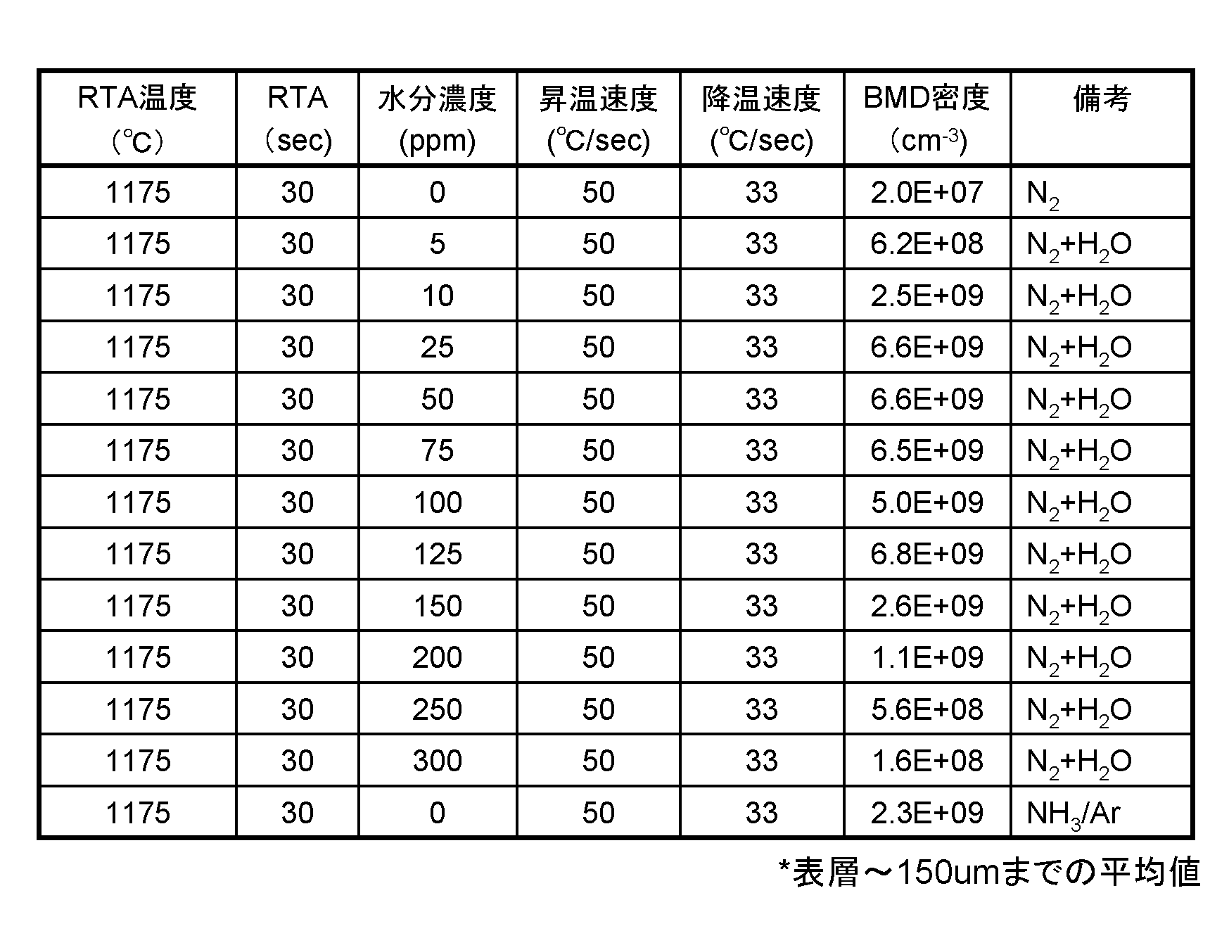
図1、表2からわかるように、純粋な窒素ガス(N2)の雰囲気で熱処理を行った場合にはBMD密度が非常に小さいが、窒素ガスに水分を混入させた雰囲気ガス(N2+H2O(5ppm以上))で行った場合にはBMD密度が高く、RTA熱処理において十分な空孔注入が行われていることがわかる。
また、水分濃度が250ppmを超えると酸化膜が形成されてしまい、格子間Siの注入量が多くなって空孔が減るため、BMD密度が非常に小さくなっていることがわかる。
また、水分濃度が250ppmを超えると酸化膜が形成されてしまい、格子間Siの注入量が多くなって空孔が減るため、BMD密度が非常に小さくなっていることがわかる。
RTA熱処理において、実施例(N2+H2O(5~250ppm))と比較例(NH3/Ar)では共にシリコンウェーハ表面に酸窒化膜または窒化膜が形成されていたが、実施例では1nm程度の厚さで、比較例に比べてその膜厚は薄かった。しかし、実施例の方が比較例よりもBMD密度が高いケースもあった。これは、空孔注入量が多いほどBMDのサイズが小さく、サイズの小さいBMDは後の熱処理工程で消滅しやすいため、実施例の方が比較例(NH3/Ar)よりも適度な空孔注入量であったことがわかる。
このため、本発明のRTA熱処理を施したシリコンウェーハは、高温熱処理を必要とするエピタキシャル層成長用ウェーハに好適であることがわかる。
このため、本発明のRTA熱処理を施したシリコンウェーハは、高温熱処理を必要とするエピタキシャル層成長用ウェーハに好適であることがわかる。
なお、本発明は、上記実施形態に限定されるものではない。上記実施形態は単なる例示であり、本発明の特許請求の範囲に記載された技術的思想と実質的に同一な構成を有し、同様な作用効果を奏するものは、いかなるものであっても本発明の技術的範囲に包含される。
Claims (6)
- 少なくとも、雰囲気ガス中でシリコンウェーハにRTA熱処理を施す工程を有するシリコンウェーハの製造方法であって、前記雰囲気ガスとして、窒素ガスに5ppm以上250ppm以下の濃度の水分を混入させたものを用いてRTA熱処理を施すことを特徴とするシリコンウェーハの製造方法。
- 前記雰囲気ガスとして、窒素ガスに10ppm以上150ppm以下の濃度の水分を混入させたものを用いることを特徴とする請求項1に記載のシリコンウェーハの製造方法。
- 前記雰囲気ガスとして、窒素ガスの露点を制御することにより窒素ガスに混入させる水分の濃度を調整することを特徴とする請求項1又は請求項2に記載のシリコンウェーハの製造方法。
- 前記雰囲気ガスとして、窒素ガスの露点を-60℃以上-38℃以下に制御することにより、窒素ガスに10ppm以上150ppm以下の濃度の水分を混入させることを特徴とする請求項2又は請求項3に記載のシリコンウェーハの製造方法。
- 前記RTA熱処理が施されるシリコンウェーハの初期酸素濃度を、9ppma以上14ppma以下とすることを特徴とする請求項1乃至請求項4のいずれか一項に記載のシリコンウェーハの製造方法。
- 前記RTA熱処理が施されたシリコンウェーハの表面に、エピタキシャル層を成長させることを特徴とする請求項1乃至請求項5のいずれか一項に記載のシリコンウェーハの製造方法。
Applications Claiming Priority (2)
| Application Number | Priority Date | Filing Date | Title |
|---|---|---|---|
| JP2008278775A JP2010109100A (ja) | 2008-10-29 | 2008-10-29 | シリコンウェーハの製造方法 |
| JP2008-278775 | 2008-10-29 |
Publications (1)
| Publication Number | Publication Date |
|---|---|
| WO2010050120A1 true WO2010050120A1 (ja) | 2010-05-06 |
Family
ID=42128493
Family Applications (1)
| Application Number | Title | Priority Date | Filing Date |
|---|---|---|---|
| PCT/JP2009/004955 Ceased WO2010050120A1 (ja) | 2008-10-29 | 2009-09-29 | シリコンウェーハの製造方法 |
Country Status (3)
| Country | Link |
|---|---|
| JP (1) | JP2010109100A (ja) |
| TW (1) | TW201025454A (ja) |
| WO (1) | WO2010050120A1 (ja) |
Cited By (2)
| Publication number | Priority date | Publication date | Assignee | Title |
|---|---|---|---|---|
| CN102168312A (zh) * | 2011-03-09 | 2011-08-31 | 浙江大学 | 一种高掺氮的硅片及其快速掺氮的方法 |
| GB2574879B (en) * | 2018-06-22 | 2022-12-28 | X Fab Semiconductor Foundries Gmbh | Substrates for III-nitride epitaxy |
Families Citing this family (2)
| Publication number | Priority date | Publication date | Assignee | Title |
|---|---|---|---|---|
| JP5530856B2 (ja) * | 2010-08-18 | 2014-06-25 | 信越半導体株式会社 | ウエーハの熱処理方法及びシリコンウエーハの製造方法並びに熱処理装置 |
| JP5333620B2 (ja) * | 2012-03-14 | 2013-11-06 | 信越半導体株式会社 | エピタキシャルシリコンウェーハの製造方法 |
Citations (3)
| Publication number | Priority date | Publication date | Assignee | Title |
|---|---|---|---|---|
| JP2003031582A (ja) * | 2000-11-28 | 2003-01-31 | Sumitomo Mitsubishi Silicon Corp | シリコンウェーハの製造方法及びシリコンウェーハ |
| JP2004537161A (ja) * | 2001-04-11 | 2004-12-09 | エムイーエムシー・エレクトロニック・マテリアルズ・インコーポレイテッド | 高抵抗率czシリコンにおけるサーマルドナー生成の制御 |
| JP2008016652A (ja) * | 2006-07-06 | 2008-01-24 | Shin Etsu Handotai Co Ltd | シリコンウェーハの製造方法 |
-
2008
- 2008-10-29 JP JP2008278775A patent/JP2010109100A/ja active Pending
-
2009
- 2009-09-29 WO PCT/JP2009/004955 patent/WO2010050120A1/ja not_active Ceased
- 2009-10-07 TW TW098134031A patent/TW201025454A/zh unknown
Patent Citations (3)
| Publication number | Priority date | Publication date | Assignee | Title |
|---|---|---|---|---|
| JP2003031582A (ja) * | 2000-11-28 | 2003-01-31 | Sumitomo Mitsubishi Silicon Corp | シリコンウェーハの製造方法及びシリコンウェーハ |
| JP2004537161A (ja) * | 2001-04-11 | 2004-12-09 | エムイーエムシー・エレクトロニック・マテリアルズ・インコーポレイテッド | 高抵抗率czシリコンにおけるサーマルドナー生成の制御 |
| JP2008016652A (ja) * | 2006-07-06 | 2008-01-24 | Shin Etsu Handotai Co Ltd | シリコンウェーハの製造方法 |
Cited By (4)
| Publication number | Priority date | Publication date | Assignee | Title |
|---|---|---|---|---|
| CN102168312A (zh) * | 2011-03-09 | 2011-08-31 | 浙江大学 | 一种高掺氮的硅片及其快速掺氮的方法 |
| GB2574879B (en) * | 2018-06-22 | 2022-12-28 | X Fab Semiconductor Foundries Gmbh | Substrates for III-nitride epitaxy |
| DE102019116743B4 (de) | 2018-06-22 | 2025-02-27 | X-Fab Semiconductor Foundries Gmbh | Verfahren zur Herstellung eines Wafers für Gruppe-III-Nitrid-Epitaxie |
| US12331426B2 (en) | 2018-06-22 | 2025-06-17 | X-Fab Semiconductor Foundries Gmbh | Substrates for III-nitride epitaxy |
Also Published As
| Publication number | Publication date |
|---|---|
| JP2010109100A (ja) | 2010-05-13 |
| TW201025454A (en) | 2010-07-01 |
Similar Documents
| Publication | Publication Date | Title |
|---|---|---|
| JP4720058B2 (ja) | シリコンウェーハの製造方法 | |
| US6843848B2 (en) | Semiconductor wafer made from silicon and method for producing the semiconductor wafer | |
| TWI628320B (zh) | Heat treatment of single crystal germanium wafer | |
| TW200818322A (en) | Silicon wafer manufacturing method | |
| WO2010050120A1 (ja) | シリコンウェーハの製造方法 | |
| JP5062217B2 (ja) | 半導体ウェーハの製造方法 | |
| TWI855103B (zh) | 摻雜碳之矽單晶晶圓及其製造方法 | |
| US20120049330A1 (en) | Silicon wafer and method for producing the same | |
| JP3791446B2 (ja) | エピタキシャルウェーハの製造方法及びエピタキシャルウェーハ | |
| CN106048732A (zh) | 硅晶片的制造方法 | |
| JP5045710B2 (ja) | シリコンウェーハの製造方法 | |
| JP2009177194A (ja) | シリコンウェーハの製造方法、シリコンウェーハ | |
| JP4345253B2 (ja) | エピタキシャルウェーハの製造方法及びエピタキシャルウェーハ | |
| CN111788662B (zh) | 单晶硅晶圆的热处理方法 | |
| JP2010114211A (ja) | エピタキシャルシリコンウェーハの製造方法 | |
| JP2003007711A (ja) | シリコンウェーハ | |
| JP5333620B2 (ja) | エピタキシャルシリコンウェーハの製造方法 | |
| JP5434239B2 (ja) | シリコンウェーハの製造方法 | |
| JP2003077924A (ja) | 半導体ウェーハの製造方法及び半導体ウェーハ |
Legal Events
| Date | Code | Title | Description |
|---|---|---|---|
| 121 | Ep: the epo has been informed by wipo that ep was designated in this application |
Ref document number: 09823235 Country of ref document: EP Kind code of ref document: A1 |
|
| NENP | Non-entry into the national phase |
Ref country code: DE |
|
| 122 | Ep: pct application non-entry in european phase |
Ref document number: 09823235 Country of ref document: EP Kind code of ref document: A1 |