WO2010035703A1 - 半導体部材製造方法及び粘着テープ - Google Patents
半導体部材製造方法及び粘着テープ Download PDFInfo
- Publication number
- WO2010035703A1 WO2010035703A1 PCT/JP2009/066343 JP2009066343W WO2010035703A1 WO 2010035703 A1 WO2010035703 A1 WO 2010035703A1 JP 2009066343 W JP2009066343 W JP 2009066343W WO 2010035703 A1 WO2010035703 A1 WO 2010035703A1
- Authority
- WO
- WIPO (PCT)
- Prior art keywords
- semiconductor member
- adhesive
- acrylate
- meth
- adhesive tape
- Prior art date
- Legal status (The legal status is an assumption and is not a legal conclusion. Google has not performed a legal analysis and makes no representation as to the accuracy of the status listed.)
- Ceased
Links
Images





Classifications
-
- C—CHEMISTRY; METALLURGY
- C09—DYES; PAINTS; POLISHES; NATURAL RESINS; ADHESIVES; COMPOSITIONS NOT OTHERWISE PROVIDED FOR; APPLICATIONS OF MATERIALS NOT OTHERWISE PROVIDED FOR
- C09J—ADHESIVES; NON-MECHANICAL ASPECTS OF ADHESIVE PROCESSES IN GENERAL; ADHESIVE PROCESSES NOT PROVIDED FOR ELSEWHERE; USE OF MATERIALS AS ADHESIVES
- C09J4/00—Adhesives based on organic non-macromolecular compounds having at least one polymerisable carbon-to-carbon unsaturated bond ; adhesives, based on monomers of macromolecular compounds of groups C09J183/00 - C09J183/16
-
- C—CHEMISTRY; METALLURGY
- C08—ORGANIC MACROMOLECULAR COMPOUNDS; THEIR PREPARATION OR CHEMICAL WORKING-UP; COMPOSITIONS BASED THEREON
- C08G—MACROMOLECULAR COMPOUNDS OBTAINED OTHERWISE THAN BY REACTIONS ONLY INVOLVING UNSATURATED CARBON-TO-CARBON BONDS
- C08G18/00—Polymeric products of isocyanates or isothiocyanates
- C08G18/06—Polymeric products of isocyanates or isothiocyanates with compounds having active hydrogen
- C08G18/28—Polymeric products of isocyanates or isothiocyanates with compounds having active hydrogen characterised by the compounds used containing active hydrogen
- C08G18/40—High-molecular-weight compounds
- C08G18/48—Polyethers
- C08G18/4825—Polyethers containing two hydroxy groups
-
- C—CHEMISTRY; METALLURGY
- C08—ORGANIC MACROMOLECULAR COMPOUNDS; THEIR PREPARATION OR CHEMICAL WORKING-UP; COMPOSITIONS BASED THEREON
- C08G—MACROMOLECULAR COMPOUNDS OBTAINED OTHERWISE THAN BY REACTIONS ONLY INVOLVING UNSATURATED CARBON-TO-CARBON BONDS
- C08G18/00—Polymeric products of isocyanates or isothiocyanates
- C08G18/06—Polymeric products of isocyanates or isothiocyanates with compounds having active hydrogen
- C08G18/28—Polymeric products of isocyanates or isothiocyanates with compounds having active hydrogen characterised by the compounds used containing active hydrogen
- C08G18/67—Unsaturated compounds having active hydrogen
- C08G18/671—Unsaturated compounds having only one group containing active hydrogen
- C08G18/672—Esters of acrylic or alkyl acrylic acid having only one group containing active hydrogen
-
- C—CHEMISTRY; METALLURGY
- C08—ORGANIC MACROMOLECULAR COMPOUNDS; THEIR PREPARATION OR CHEMICAL WORKING-UP; COMPOSITIONS BASED THEREON
- C08G—MACROMOLECULAR COMPOUNDS OBTAINED OTHERWISE THAN BY REACTIONS ONLY INVOLVING UNSATURATED CARBON-TO-CARBON BONDS
- C08G18/00—Polymeric products of isocyanates or isothiocyanates
- C08G18/06—Polymeric products of isocyanates or isothiocyanates with compounds having active hydrogen
- C08G18/70—Polymeric products of isocyanates or isothiocyanates with compounds having active hydrogen characterised by the isocyanates or isothiocyanates used
- C08G18/72—Polyisocyanates or polyisothiocyanates
- C08G18/80—Masked polyisocyanates
- C08G18/8003—Masked polyisocyanates masked with compounds having at least two groups containing active hydrogen
- C08G18/8006—Masked polyisocyanates masked with compounds having at least two groups containing active hydrogen with compounds of C08G18/32
- C08G18/8009—Masked polyisocyanates masked with compounds having at least two groups containing active hydrogen with compounds of C08G18/32 with compounds of C08G18/3203
- C08G18/8022—Masked polyisocyanates masked with compounds having at least two groups containing active hydrogen with compounds of C08G18/32 with compounds of C08G18/3203 with polyols having at least three hydroxy groups
- C08G18/8025—Masked aliphatic or cycloaliphatic polyisocyanates
-
- C—CHEMISTRY; METALLURGY
- C09—DYES; PAINTS; POLISHES; NATURAL RESINS; ADHESIVES; COMPOSITIONS NOT OTHERWISE PROVIDED FOR; APPLICATIONS OF MATERIALS NOT OTHERWISE PROVIDED FOR
- C09J—ADHESIVES; NON-MECHANICAL ASPECTS OF ADHESIVE PROCESSES IN GENERAL; ADHESIVE PROCESSES NOT PROVIDED FOR ELSEWHERE; USE OF MATERIALS AS ADHESIVES
- C09J175/00—Adhesives based on polyureas or polyurethanes; Adhesives based on derivatives of such polymers
- C09J175/04—Polyurethanes
- C09J175/14—Polyurethanes having carbon-to-carbon unsaturated bonds
- C09J175/16—Polyurethanes having carbon-to-carbon unsaturated bonds having terminal carbon-to-carbon unsaturated bonds
-
- C—CHEMISTRY; METALLURGY
- C09—DYES; PAINTS; POLISHES; NATURAL RESINS; ADHESIVES; COMPOSITIONS NOT OTHERWISE PROVIDED FOR; APPLICATIONS OF MATERIALS NOT OTHERWISE PROVIDED FOR
- C09J—ADHESIVES; NON-MECHANICAL ASPECTS OF ADHESIVE PROCESSES IN GENERAL; ADHESIVE PROCESSES NOT PROVIDED FOR ELSEWHERE; USE OF MATERIALS AS ADHESIVES
- C09J7/00—Adhesives in the form of films or foils
- C09J7/20—Adhesives in the form of films or foils characterised by their carriers
- C09J7/22—Plastics; Metallised plastics
-
- C—CHEMISTRY; METALLURGY
- C09—DYES; PAINTS; POLISHES; NATURAL RESINS; ADHESIVES; COMPOSITIONS NOT OTHERWISE PROVIDED FOR; APPLICATIONS OF MATERIALS NOT OTHERWISE PROVIDED FOR
- C09J—ADHESIVES; NON-MECHANICAL ASPECTS OF ADHESIVE PROCESSES IN GENERAL; ADHESIVE PROCESSES NOT PROVIDED FOR ELSEWHERE; USE OF MATERIALS AS ADHESIVES
- C09J7/00—Adhesives in the form of films or foils
- C09J7/30—Adhesives in the form of films or foils characterised by the adhesive composition
- C09J7/38—Pressure-sensitive adhesives [PSA]
-
- H—ELECTRICITY
- H10—SEMICONDUCTOR DEVICES; ELECTRIC SOLID-STATE DEVICES NOT OTHERWISE PROVIDED FOR
- H10P—GENERIC PROCESSES OR APPARATUS FOR THE MANUFACTURE OR TREATMENT OF DEVICES COVERED BY CLASS H10
- H10P72/00—Handling or holding of wafers, substrates or devices during manufacture or treatment thereof
- H10P72/04—Apparatus for manufacture or treatment
- H10P72/0442—Apparatus for placing on an insulating substrate, e.g. tape
-
- C—CHEMISTRY; METALLURGY
- C09—DYES; PAINTS; POLISHES; NATURAL RESINS; ADHESIVES; COMPOSITIONS NOT OTHERWISE PROVIDED FOR; APPLICATIONS OF MATERIALS NOT OTHERWISE PROVIDED FOR
- C09J—ADHESIVES; NON-MECHANICAL ASPECTS OF ADHESIVE PROCESSES IN GENERAL; ADHESIVE PROCESSES NOT PROVIDED FOR ELSEWHERE; USE OF MATERIALS AS ADHESIVES
- C09J2203/00—Applications of adhesives in processes or use of adhesives in the form of films or foils
- C09J2203/326—Applications of adhesives in processes or use of adhesives in the form of films or foils for bonding electronic components such as wafers, chips or semiconductors
-
- C—CHEMISTRY; METALLURGY
- C09—DYES; PAINTS; POLISHES; NATURAL RESINS; ADHESIVES; COMPOSITIONS NOT OTHERWISE PROVIDED FOR; APPLICATIONS OF MATERIALS NOT OTHERWISE PROVIDED FOR
- C09J—ADHESIVES; NON-MECHANICAL ASPECTS OF ADHESIVE PROCESSES IN GENERAL; ADHESIVE PROCESSES NOT PROVIDED FOR ELSEWHERE; USE OF MATERIALS AS ADHESIVES
- C09J2423/00—Presence of polyolefin
- C09J2423/10—Presence of homo or copolymers of propene
- C09J2423/106—Presence of homo or copolymers of propene in the substrate
-
- C—CHEMISTRY; METALLURGY
- C09—DYES; PAINTS; POLISHES; NATURAL RESINS; ADHESIVES; COMPOSITIONS NOT OTHERWISE PROVIDED FOR; APPLICATIONS OF MATERIALS NOT OTHERWISE PROVIDED FOR
- C09J—ADHESIVES; NON-MECHANICAL ASPECTS OF ADHESIVE PROCESSES IN GENERAL; ADHESIVE PROCESSES NOT PROVIDED FOR ELSEWHERE; USE OF MATERIALS AS ADHESIVES
- C09J2433/00—Presence of (meth)acrylic polymer
Definitions
- the present invention relates to a method for producing a semiconductor member and an adhesive tape used in these methods.
- an electronic device such as an IC (Integrated Circuit) card, a mobile phone, and a PDA (Personal Digital Assistant) has a chip-shaped electronic component on which a circuit pattern is formed.
- IC Integrated Circuit
- PDA Personal Digital Assistant
- a semiconductor member is formed by dividing a semiconductor member in which a plurality of circuit patterns are formed on a semiconductor wafer such as silicon or gallium-arsenide, an insulating substrate, etc. Is also becoming thinner (see Patent Document 1).
- the semiconductor member when the thinned semiconductor member is separated into pieces by a dicing blade having diamond abrasive grains, the semiconductor member may be cracked.
- an adhesive resin is applied to a semiconductor member, the semiconductor member is temporarily fixed to a fixing jig via the adhesive resin, and an individualized process for separating the semiconductor member, and an individualized semiconductor Adhering from a separated semiconductor member by immersing it in a liquid in a temperature range between the adhesive tape and the adhesive resin lowering temperature X of the adhesive resin and the heat shrink temperature Y of the adhesive tape.
- a method for manufacturing a semiconductor member which includes a transfer step of peeling the adhesive resin and the fixing jig and transferring the semiconductor member to the adhesive tape, and a pickup step of picking up the individual semiconductor member on the adhesive tape.
- an adhesive resin is applied to the semiconductor member, the semiconductor member is temporarily fixed to the fixing jig via the adhesive resin, and the individualization process is performed.
- a semiconductor member manufacturing method including a two-peeling step and a pickup step of picking up an individual semiconductor member on an adhesive tape.
- the temperature of the liquid used in the transfer process is 40 ° C. or higher and 100 ° C. or lower.
- the side of the semiconductor member to which the adhesive tape is attached is directed upward, and the side of the semiconductor member to which the adhesive resin and the fixing jig are attached is directed downward. Immerse in liquid.
- the fixing jig is allowed to fall freely together with the adhesive resin by floating the semiconductor member in the liquid via the adhesive tape.
- the base film of the pressure-sensitive adhesive tape is a propylene-based copolymer.
- the pressure-sensitive adhesive layer of the pressure-sensitive adhesive tape comprises 100 parts by weight of a (meth) acrylic acid ester copolymer, 0.5 parts by weight or more and 20 parts by weight or less of a polyfunctional isocyanate-based curing agent.
- the urethane acrylate oligomer having 4 or more is contained in an amount of 20 to 200 parts by mass, and the silicon-modified acrylic resin is 0.1 to 10 parts by mass.
- ⁇ ⁇ According to the present invention, it is possible to provide a semiconductor member manufacturing method that is excellent in releasability, transferability, and pickup properties.
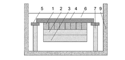
- FIG. 1 The schematic of the cross section which shows the state pulled up from the warm water 6 after the transfer process using the peeling tape 8.
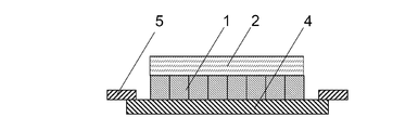
- FIG. The schematic of the cross section which shows the state which affixed the peeling tape 8 on the surface of the adhesive resin 2.
- FIG. The schematic of the cross section which shows the state which peeled off the peeling tape 8 with the adhesive resin 2.
- the semiconductor member manufacturing method includes an individualizing step in which an adhesive resin is applied to the semiconductor member, the semiconductor member is temporarily fixed to a fixing jig via the adhesive resin, and is separated into individual pieces.
- a semiconductor member manufacturing method comprising: a transfer step of peeling an adhesive resin and a fixing jig from a semiconductor member, and transferring the semiconductor member to an adhesive tape; and a pickup step of picking up an individual semiconductor member on the adhesive tape Is the method.
- ⁇ Individualization process> As a semiconductor member used in the singulation process in which an adhesive resin is applied to a semiconductor member, the semiconductor member is temporarily fixed to a fixing jig via the adhesive resin, and is divided into pieces, a disk-shaped silicon wafer Glass, gallium arsenide (GaAs).
- As the adhesive resin an acrylic resin or an epoxy resin is preferably used.
- Fixing jigs include glass and ceramic.
- the bonding step of bonding the adhesive tape to the separated semiconductor member is not laminated with the adhesive resin of the semiconductor member that has been separated into individual pieces but maintained in a disc shape as a whole.
- This is a process of sticking an adhesive tape to the surface, and the method of bonding includes, for example, roll pressure bonding and vacuum pressure bonding.
- the transfer step of transferring the film to the adhesive tape means that the semiconductor member is transferred to the adhesive tape by peeling the adhesive resin and the fixing jig from the semiconductor member.
- the transfer step can be achieved by immersing the transfer step in a liquid in a temperature range between the adhesive force lowering temperature X of the adhesive resin and the heat shrink temperature Y of the adhesive tape.
- the adhesive resin lowering temperature X of the adhesive resin and the heat shrink temperature Y of the pressure-sensitive adhesive tape need to satisfy the relationship X ⁇ Y, and the liquid temperature T needs to satisfy the relationship X ⁇ T ⁇ Y. .
- Adhesive strength drop temperature varies depending on the adhesive resin and the synthetic resin used as the base film of the adhesive tape. If the lower limit of the set temperature T of the liquid is low, the adhesive strength of the adhesive resin is less likely to decrease. Yes, if the upper limit of the set value is high, the adhesive tape tends to shrink.
- the set temperature of the liquid is 40 ° C., preferably 75 ° C. as the lower limit, and 120 ° C., preferably 100 ° C. as the upper limit.
- the liquid includes water and oil, but water is preferable in view of the influence on the semiconductor member.
- the adhesive tape, the semiconductor member, the adhesive resin, and the fixing jig are arranged from above to be immersed in the liquid. That is, in the transfer step, it is preferable that the semiconductor member is immersed in the liquid with the side to which the adhesive tape is attached facing upward and the side of the semiconductor member to which the adhesive resin and the fixing jig are attached facing downward. By dipping in this arrangement, the adhesive resin can be peeled off due to its own weight with the fixing jig and a decrease in the adhesive strength of the adhesive resin.
- the peeling tape is bonded to the adhesive resin, and the peeling tape is peeled off from the separated semiconductor member together with the adhesive resin.
- the pressure-sensitive adhesive tape is composed of a base material and a pressure-sensitive adhesive layer, and a pressure-sensitive adhesive having a pressure-sensitive adhesive force lowering temperature higher than that of the adhesive resin is laminated.
- the base material of the adhesive tape is preferably a material that does not undergo deformation such as expansion and contraction even when immersed, and is preferably a synthetic resin or metal.
- Examples of the shape of the substrate include a film, a sheet, and a foil.
- the thickness of the substrate is preferably 50 ⁇ m or more and 250 ⁇ m or less. A more preferable lower limit is 70 ⁇ m, and a more preferable upper limit is 150 ⁇ m. When the thickness of the substrate is reduced, the substrate tends to be cut during expansion in the pickup process, and when the thickness of the substrate is increased, the expandability tends to be inferior.
- Synthetic resins used as the base material for adhesive tape include PVC (polyvinyl chloride), polyethylene, PET (polyethylene terephthalate), EVA (ethylene-vinyl acetate copolymer), ethylene-ethyl acrylate copolymer, polypropylene, propylene Copolymer, ethylene-acrylic acid copolymer, ionomer resin, and polyimide.
- PET and propylene copolymer are preferable, and propylene copolymer is more preferable.
- the metal used as the base material of the adhesive tape include stainless steel, copper, and aluminum.
- the base material may be a mixture of these synthetic resins, a copolymer, a laminate of synthetic resins, a laminate of metals, or a laminate of synthetic resin and metal.
- propylene-based copolymer examples include a random copolymer of propylene and other components, a block copolymer of propylene and other components, and an alternating copolymer of propylene and other components.
- other components include ⁇ -olefins such as ethylene, 1-butene, 1-pentene, 1-hexene and 1-heptene, copolymers composed of at least two kinds of ⁇ -olefins, and styrene-diene copolymers. Can be mentioned. Of these, 1-butene is preferred. Thereby, it is possible to particularly suppress chips generated when the semiconductor member is cut.
- Adhesive for adhesive tape polymers obtained by polymerizing acrylic acid, methacrylic acid and their ester monomers, and unsaturated monomers copolymerizable with these monomers (eg, vinyl acetate, styrene, acrylonitrile) are copolymerized.
- (meth) acrylic acid ester copolymers are preferred.
- the pressure-sensitive adhesive layer has a low molecular weight compound having at least two photopolymerizable carbon-carbon double bonds in the molecule that can be three-dimensionally reticulated by irradiation with ultraviolet rays or radiation, such as an acrylate compound or a urethane acrylate oligomer.
- a photo-curing pressure-sensitive adhesive using can also be employed.
- the (meth) acrylic acid ester copolymer used as the adhesive for the adhesive tape is not particularly limited, but is a copolymer of the main monomer of (meth) acrylic acid ester and other vinyl compound monomers. is there.
- the vinyl compound monomer is one or more of a functional group consisting of a hydroxyl group, a carboxyl group, an epoxy group, an amide group, an amino group, a methylol group, a sulfonic acid group, a sulfamic acid group, and a (phosphite) ester group. It is preferable to use a functional group-containing monomer having
- (meth) acrylic acid ester for example, butyl (meth) acrylate, 2-butyl (meth) acrylate, t-butyl (meth) acrylate, pentyl (meth) acrylate, octyl (meth) acrylate, 2 -Ethylhexyl (meth) acrylate, nonyl (meth) acrylate, decyl (meth) acrylate, lauryl (meth) acrylate, methyl (meth) acrylate, ethyl (meth) acrylate, isopropyl (meth) acrylate, tridecyl (meth) acrylate, myristyl (Meth) acrylate, cetyl (meth) acrylate, stearyl (meth) acrylate, cyclohexyl (meth) acrylate, isobornyl (meth) acrylate, dicyclopentanyl (meth) acrylate,
- a functional group-containing monomer for example, a vinyl compound having a hydroxyl group, a carboxyl group, an epoxy group, an amide group, an amino group, a methylol group, a sulfonic acid group, a sulfamic acid group, or a (sub) phosphate group as a functional group Is mentioned.
- Examples of the monomer having a hydroxyl group include 2-hydroxyethyl (meth) acrylate, 2-hydroxypropyl (meth) acrylate, 2-hydroxybutyl (meth) acrylate, and the like.
- Examples of the monomer having a carboxyl group include (meth) acrylic acid, crotonic acid, maleic acid, maleic anhydride, itaconic acid, fumaric acid, acrylamide N-glycolic acid, and cinnamic acid.
- Examples of the monomer having an epoxy group include allyl glycidyl ether and (meth) acrylic acid glycidyl ether.
- Examples of the monomer having an amide group include (meth) acrylamide.
- Examples of the monomer having an amino group include N, N-dimethylaminoethyl (meth) acrylate.
- Examples of the monomer having a methylol group include N-methylolacrylamide.
- a known method such as emulsion polymerization or solution polymerization can be used as a method for producing a (meth) acrylic acid ester copolymer.
- Acrylic rubber that can be produced by emulsion polymerization is preferred so that the adhesive tape can be easily separated from the semiconductor member after irradiation.
- the polyfunctional isocyanate curing agent used as the adhesive of the adhesive tape is not particularly limited except that it has two or more isocyanate groups, and examples thereof include aromatic polyisocyanates, aliphatic polyisocyanates, and alicyclic polyisocyanates.
- the aromatic polyisocyanate is not particularly limited, and for example, 1,3-phenylene diisocyanate, 4,4′-diphenyl diisocyanate, 1,4-phenylene diisocyanate, 4,4′-diphenylmethane diisocyanate, 2,4-tolylene diisocyanate, 2, , 6-tolylene diisocyanate, 4,4′-toluidine diisocyanate, 2,4,6-triisocyanate toluene, 1,3,5-triisocyanate benzene, dianisidine diisocyanate, 4,4′-diphenyl ether diisocyanate, 4,4 ', 4 "-triphenylmethane triisocyanate, ⁇ , ⁇ '-diisocyanate-1,3-dimethylbenzene, ⁇ , ⁇ '-diisocyanate-1,4-dimethylbenzene, ⁇ , ⁇ '-diisocyanate-1,4- Diechi
- the aliphatic polyisocyanate is not particularly limited.
- diisocyanate and 2,4,4-trimethylhexamethylene diisocyanate examples thereof include diisocyanate and 2,4,4-trimethylhexamethylene diisocyanate.
- the alicyclic polyisocyanate is not particularly limited.
- 1,3-phenylene diisocyanate, 4,4'-diphenyl diisocyanate, 1,4-phenylene diisocyanate, 4,4'-diphenylmethane diisocyanate, 2,4-tolylene diisocyanate, 2,6-tolylene diisocyanate 4,4′-toluidine diisocyanate and hexamethylene diisocyanate are preferably used.
- the blending ratio of the polyfunctional isocyanate curing agent is preferably 0.1 parts by mass or more and 20 parts by mass or less with respect to 100 parts by mass of ((meth) acrylic acid ester copolymer), and the lower limit is 0.5 parts by mass. Is more preferably 10 parts by mass. If the polyfunctional isocyanate curing agent is 0.1 part by mass or more, the adhesive force is not too strong, and hence the occurrence of pickup failure can be suppressed. Moreover, if a polyfunctional isocyanate hardening
- curing agent is 20 mass parts or less, since adhesive force does not fall and the retainability of the separated semiconductor member in the transfer process at the time of liquid immersion is maintained, it is preferable.
- urethane acrylate oligomers with 4 or more vinyl groups A urethane acrylate oligomer having 4 or more vinyl groups (hereinafter simply referred to as “urethane acrylate oligomer”) used as an adhesive for an adhesive tape has 4 or more vinyl groups and has a urethane bond in the molecule. If it is a (meth) acrylate oligomer, it will not specifically limit.
- the method for producing the urethane acrylate oligomer is not particularly limited.
- a urethane acrylate is prepared by reacting a (meth) acrylate compound containing a hydroxyl group and a plurality of (meth) acrylate groups with a compound having a plurality of isocyanate groups (for example, a diisocyanate compound).
- a compound having a plurality of isocyanate groups for example, a diisocyanate compound.
- An example is an oligomer method.
- a compound having a plurality of isocyanate groups for example, a diisocyanate compound
- a compound having a plurality of isocyanate groups for example, a diisocyanate compound
- a compound having a plurality of isocyanate groups is added and reacted to form an oligomer having a plurality of isocyanate ends, and further a hydroxyl group and a plurality of (meth) acrylate groups. It is good also as a urethane acrylate oligomer by making it react with the (meth) acrylate compound containing this.
- Examples of the (meth) acrylate compound containing a hydroxyl group and a plurality of (meth) acrylate groups include, for example, hydroxypropylated trimethylolpropane triacrylate, pentaerythritol triacrylate, dipentaerythritol-hydroxy-pentaacrylate, and bis (pentaerythritol).
- isocyanate having a plurality of isocyanate groups examples include aromatic isocyanate, alicyclic isocyanate, and aliphatic isocyanate. Of these isocyanates, aromatic isocyanates or alicyclic isocyanates having a plurality of isocyanate groups are preferably used.
- As the form of the isocyanate component there are a monomer, a dimer, and a trimer, and a trimer is preferably used.
- aromatic diisocyanate examples include tolylene diisocyanate, 4,4-diphenylmethane diisocyanate, and xylylene diisocyanate.
- Examples of the alicyclic diisocyanate include isophorone diisocyanate and methylene bis (4-cyclohexyl isocyanate).
- Examples of the fatty diisocyanate include hexamethylene diisocyanate and trimethylhexamethylene diisocyanate.
- polyol component examples include poly (propylene oxide) diol, poly (propylene oxide) triol, copoly (ethylene oxide-propylene oxide) diol, poly (tetramethylene oxide) diol, ethoxylated bisphenol A, and ethoxylated bisphenol S spiroglycol. , Caprolactone-modified diol, carbonate diol and the like.
- the number of vinyl groups of the urethane acrylate oligomer having a vinyl group is 4 or more, it is easy to peel off the adhesive tape after irradiation from the semiconductor member, so that the pickup property can be improved.
- the compounding quantity of the urethane acrylate oligomer which has 4 or more vinyl groups is not specifically limited, It is preferable to set it as 20 to 200 mass parts with respect to 100 mass parts of (meth) acrylic acid ester copolymers. If the compounding amount of the urethane acrylate oligomer having 4 or more vinyl groups is 20 parts by mass or more, the adhesive tape after radiation irradiation can be easily peeled off from the semiconductor member, and the occurrence of pickup problems can be suppressed. . Moreover, if the compounding quantity of the urethane acrylate oligomer which has four or more vinyl groups is 200 mass parts or less, the retainability of the separated semiconductor member in the transfer process at the time of immersion in a liquid can be maintained. .
- Silicone-modified acrylic resin used as an adhesive for adhesive tape is a polymer of a (meth) acrylic monomer and a monomer having a vinyl group at the end of a polydimethylsiloxane bond (hereinafter referred to as “silicon-based macromonomer”). Yes, with the exception of having a monomer unit derived from a monomer having a vinyl group at the end of a polydimethylsiloxane bond, such as a homopolymer of a silicon-based macromonomer or a silicon-based macromonomer and other vinyl compounds And vinyl polymers obtained by polymerizing.
- a compound in which the terminal of the polydimethylsiloxane bond is a vinyl group such as a (meth) acryloyl group or a styryl group is preferably used (see, for example, JP-A-2000-080135).
- Examples of the (meth) acrylic monomer include hydroxyalkyl (meth) acrylate, modified hydroxy (meth) acrylate, and (meth) acrylic acid in addition to alkyl (meth) acrylate.
- alkyl (meth) acrylate examples include methyl (meth) acrylate, ethyl (meth) acrylate, n-propyl (meth) acrylate, n-butyl (meth) acrylate, isobutyl (meth) acrylate, and t-butyl (meth) acrylate.
- Examples of the hydroxyalkyl (meth) acrylate include hydroxyethyl (meth) acrylate, hydroxypropyl (meth) acrylate, and hydroxybutyl (meth) acrylate.
- Examples of the modified hydroxy (meth) acrylate include ethylene oxide-modified hydroxy (meth-2) acrylate and lactone-modified hydroxy (meth) acrylate.
- reactive hydroxyalkyl (meth) acrylate or modified hydroxy (meth) acrylate, and silicon-modified acrylic resin having at least one vinyl group are preferably used.
- the ratio of the silicon-based macromonomer unit in the silicon-modified acrylic resin is not particularly limited, but the silicon-based macromonomer unit is preferably 15 parts by mass or more and 50 parts by mass or less in 100 parts by mass of the silicon-modified acrylic resin.
- the content of the silicon-based macromonomer unit is 15 parts by mass or more, the adhesive tape after radiation irradiation can be easily peeled from the semiconductor member, and pickup properties can be improved.
- content of a silicon-type macromonomer unit is 50 mass parts or less, the retainability of the semiconductor member separated into pieces in the transfer process at the time of immersion in a liquid can be maintained.
- the compounding quantity of a silicon modified acrylic resin is not specifically limited, It is preferable to set it as 0.1 to 10 mass parts with respect to 100 mass parts of (meth) acrylic acid ester polymers.
- the blending amount of the silicon-modified acrylic resin is 0.1 parts by mass or more, the pressure-sensitive adhesive tape after radiation irradiation can be easily peeled from the semiconductor member, and pickup properties can be improved.
- silicone modified acrylic resin is 10 mass parts or less, the retainability of the separated semiconductor member in the transfer process at the time of immersion in a liquid can be maintained.
- additives such as a polymerization initiator, a softener, an anti-aging agent, a filler, an ultraviolet absorber, and a light stabilizer may be added to the adhesive layer.
- the thickness of the adhesive layer is not particularly limited, but is generally about 5 ⁇ m to 100 ⁇ m, and preferably about 5 ⁇ m to 40 ⁇ m.
- the method of forming an adhesive layer on a substrate film to form an adhesive tape is not particularly limited.
- the adhesive is applied on the substrate with a coater such as a gravure coater, comma coater, bar coater, knife coater, or roll coater.
- a coater such as a gravure coater, comma coater, bar coater, knife coater, or roll coater.
- coating directly is mentioned.
- the pressure-sensitive adhesive layer may be printed on the substrate film by letterpress printing, intaglio printing, planographic printing, flexographic printing, offset printing, screen printing, or the like.
- the adhesive resin needs to have a relationship of X ⁇ T ⁇ Y, in which the adhesive force lowering temperature X has a relationship of X ⁇ Y with respect to the shrinkage temperature Y of the adhesive tape and is lower than the temperature T of the liquid. It is preferable that the adhesive resin does not cause misalignment with respect to the semiconductor member due to swelling even when it comes into contact with water. Specifically, it is preferable that it has hydrophobicity, or does not swell greatly or does not dissolve even when contacted with water. Examples of the adhesive resin having this property include acrylic resins, urethane adhesives, and epoxy adhesives, and acrylic resins are preferable.
- the adhesive resin is composed of (A) polyfunctional (meth) acrylate, (B) monofunctional (meth) acrylate and (C) polymerization initiator having hydrophobicity. More preferably, these blends are used in an amount of 50 to 97 (B) monofunctional (meth) acrylate with respect to 100 parts by mass of the total amount of (A) polyfunctional (meth) acrylate and (B) monofunctional (meth) acrylate. It is preferable to add 0.1 to 20 parts by mass of (C) a polymerization initiator.
- the addition amount of (A) polyfunctional (meth) acrylate is preferably 3 to 50 parts by mass in 100 parts by mass of the total amount of (A) polyfunctional (meth) acrylate and (B) monofunctional (meth) acrylate.
- ((A) polyfunctional (meth) acrylate) As the (A) polyfunctional (meth) acrylate used as the adhesive resin, two or more (meth) acryloylated polyfunctional (meth) acrylate oligomer / polymer or two or more of the oligomer / polymer terminal or side chain are used. A monomer having a (meth) acryloyl group can be used.
- polyfunctional (meth) acrylate oligomer / polymer examples include 1,2-polybutadiene-terminated urethane (meth) acrylate (for example, TE-2000, TEA-1000 manufactured by Nippon Soda Co., Ltd.), 1,2-polybutadiene-terminated urethane (meta) ) Hydrogenated acrylate (for example, TEAI-1000 manufactured by Nippon Soda Co., Ltd.), 1,4-polybutadiene terminated urethane (meth) acrylate (for example, BAC-45 manufactured by Osaka Organic Chemical Co., Ltd.), polyisoprene terminated (meth) acrylate, polyester -Based urethane (meth) acrylate, polyether-based urethane (meth) acrylate, polyester (meth) acrylate, bis-A type epoxy (meth) acrylate (for example, Biscoat # 540 manufactured by Osaka Organic Chemical Co., Ltd.,
- Examples of the trifunctional (meth) acrylate monomer include tomethylolpropane tri (meth) acrylate and tris [(meth) acryloxyethyl] isocyanurate.
- tetrafunctional or higher (meth) acrylate monomers dimethylolpropane tetra (meth) acrylate, pentaerythritol tetra (meth) acrylate, pentaerythritol ethoxytetra (meth) acrylate, dipentaerystol penta (meth) acrylate, dipenta Examples include erythrole hexa (meth) acrylate.
- (B) Monofunctional (meth) acrylate monomer examples include methyl (meth) acrylate, ethyl (meth) acrylate, propyl (meth) acrylate, butyl (meth) acrylate, and 2-ethylhexyl (meth) acrylate.
- the (C) polymerization initiator blended in the adhesive resin is preferably blended for sensitization with actinic rays of visible light or ultraviolet rays to promote photocuring of the adhesive resin.
- the agent can be used.
- the addition amount of the polymerization initiator (C) is preferably 0.1 to 20 parts by mass with respect to a total of 100 parts by mass of (A) polyfunctional (meth) acrylate and (B) monofunctional (meth) acrylate. More preferably, it is 3 to 20 parts by mass. If it is 0.1 mass part or more, the effect of hardening acceleration
- component (C) as a more preferable form, it becomes possible to cure without depending on the amount of light irradiation, and further the degree of cross-linking of the cured body of the adhesive resin is increased, resulting in misalignment during cutting. It is more preferable at the point which loses and the peelability improves.
- polymerization initiator examples include benzophenone and derivatives thereof, benzyl and derivatives thereof, entraquinone and derivatives thereof, benzoin, benzoin methyl ether, benzoin ethyl ether, benzoin propyl ether, benzoin isobutyl ether, and benzyl dimethyl ketal.
- Benzoin derivatives such as diethoxyacetophenone, acetophenone derivatives such as 4-t-butyltrichloroacetophenone, 2-dimethylaminoethylbenzoate, p-dimethylaminoethylbenzoate, diphenyldisulfide, thioxanthone and its derivatives, camphorquinone, 7,7- Dimethyl-2,3-dioxobicyclo [2.2.1] heptane-1-carboxylic acid, 7,7-dimethyl-2,3-dioxobicyclo [2.2.1] Butane-1-carboxy-2-bromoethyl ester, 7,7-dimethyl-2,3-dioxobicyclo [2.2.1] heptane-1-carboxy-2-methyl ester, 7,7-dimethyl-2 Camphorquinone derivatives such as 2,3-dioxobicyclo [2.2.1] heptane-1-carboxylic acid chlor
- a polar organic solvent may be used in the adhesive resin.
- the resin layer can easily swell upon contact with the liquid and reduce the adhesive strength.
- the addition amount of the polar organic solvent is preferably 0.5 to 10 parts by mass with respect to 100 parts by mass as the total amount of (A) polyfunctional (meth) acrylate and (B) monofunctional (meth) acrylate. If it is 0.5 parts by mass or more, releasability can be ensured, and if it is 10 parts by mass or less, the adhesive property tends to be peeled into a film without fear of lowering the initial adhesiveness.
- the polar organic solvent preferably has a boiling point of 30 ° C. or more and 200 ° C. or less in order to more reliably develop a phenomenon in which the adhesive resin is brought into contact with the liquid and the adhesive strength is lowered.
- a polar organic solvent include alcohols, ketones, and esters, and preferably alcohols.
- Examples of the alcohol include methanol, ethanol, n-propanol, isopropanol, n-butanol, isobutanol, sec-butanol, tert-butanol, n-amyl alcohol, isoamyl alcohol, 2-ethylbutyl alcohol and the like. Further, among the alcohols, methanol, ethanol, n-propanol, isopropanol, n-butanol, isobutanol, sec-butanol, and tert-butanol having a boiling point of 120 ° C. or less are preferred, and among these, methanol, ethanol More preferred are isopropanol and n-butanol.
- (A) a polyfunctional (meth) acrylate and (B) a monofunctional (meth) acrylate and (C) a particulate substance that does not dissolve in the polymerization initiator may be used together.
- the amount of the particulate material added is preferably 0.1 to 20 parts by weight, particularly 0.1 to 20 parts by weight with respect to 100 parts by weight as the total of (A) polyfunctional (meth) acrylate and (B) monofunctional (meth) acrylate. ⁇ 10 parts by mass are preferred. If it is 0.1 parts by mass or more, the film thickness of the adhesive resin is almost constant, and if it is 20 parts by mass or less, there is no fear that the initial adhesiveness is lowered.
- organic particles and inorganic particles that are generally used as the material of the particulate material.
- the organic particles include polyethylene particles, polypolypropylene particles, crosslinked polymethyl methacrylate particles, crosslinked polystyrene particles, and the like
- the inorganic particles include ceramic particles such as glass, silica, alumina, and titanium.
- the material of the particulate material is preferably spherical and has a constant particle size, little deformation of the particle, and small variation in particle size.
- Preferred organic particles having these conditions include methyl methacrylate monomers, crosslinked polymethyl methacrylate particles obtained as monodisperse particles by a known emulsion polymerization method of a styrene monomer and a crosslinkable monomer, crosslinked polystyrene particles, and inorganic particles.
- crosslinked polymethyl methacrylate particles and crosslinked polystyrene particles are more preferable from the viewpoint of storage stability such as sedimentation of particles and reactivity of the composition.
- the adhesive resin of the present invention includes various elastomers such as acrylic rubber, urethane rubber, ABS (acrylonitrile-butadiene-styrene rubber), inorganic fillers, solvents, and extenders that are generally used within the range not detracting from the object of the present invention.
- Additives such as reinforcing materials, plasticizers, thickeners, dyes, pigments, flame retardants, polymerization inhibitors, silane coupling agents, and surfactants may be used.
- the peeling tape is composed of a base material and an adhesive layer, and the adhesive strength between the adhesive resin and the peeling tape is higher than the adhesive strength between the semiconductor member and the adhesive resin.
- Base material for peeling tape As a base material for the peeling tape, a synthetic resin is preferable.
- the shape includes a film and a sheet.
- the thickness of the substrate is preferably 50 ⁇ m or more and 250 ⁇ m or less. A more preferable lower limit is 70 ⁇ m, and a more preferable upper limit is 150 ⁇ m.
- Synthetic resins used as the base material for peeling tape include PVC (polyvinyl chloride), polyethylene, PET (polyethylene terephthalate), EVA (ethylene-vinyl acetate copolymer), ethylene-ethyl acrylate copolymer, polypropylene, propylene Type copolymers, ethylene-acrylic acid copolymers, ionomer resins, and polyimides.
- PVC polyvinyl chloride
- PET polyethylene terephthalate
- EVA ethylene-vinyl acetate copolymer
- ethylene-ethyl acrylate copolymer polypropylene
- propylene Type copolymers ethylene-acrylic acid copolymers
- ionomer resins ionomer resins
- polyimides ethylene-acrylic acid copolymers
- the base material may be a mixture of these synthetic resins, a copolymer, or a laminate of synthetic resins.
- an acrylic adhesive As the adhesive for the peeling tape, an acrylic adhesive, a urethane adhesive, a silicon adhesive, and the like are preferable, and an acrylic adhesive is preferable.
- acrylic pressure-sensitive adhesives polymers obtained by polymerizing acrylic acid, methacrylic acid and ester monomers thereof, and unsaturated monomers copolymerizable with these monomers (for example, vinyl acetate, styrene, acrylonitrile) are copolymerized. Among these pressure-sensitive adhesives, (meth) acrylic acid ester copolymers are preferred.
- the pressure-sensitive adhesive layer has a low molecular weight compound such as an acrylate compound or urethane having at least two photopolymerizable carbon-carbon double bonds in the molecule that can be three-dimensionally reticulated by irradiation with ultraviolet rays or radiation.
- a photocurable pressure-sensitive adhesive using acrylate oligomer or the like can also be employed.
- additives such as a polymerization initiator, a softening agent, an anti-aging agent, a filler, an ultraviolet absorber, and a light stabilizer may be added to the pressure-sensitive adhesive layer of the peeling tape.
- the thickness of the pressure-sensitive adhesive layer of the peeling tape is not particularly limited, but is generally about 5 ⁇ m to 100 ⁇ m, preferably 5 ⁇ m as the lower limit and 40 ⁇ m as the upper limit.
- the method of forming an adhesive layer on a substrate film to form an adhesive tape is not particularly limited.
- the adhesive is applied on the substrate with a coater such as a gravure coater, comma coater, bar coater, knife coater, or roll coater.
- a coater such as a gravure coater, comma coater, bar coater, knife coater, or roll coater.
- coating directly is mentioned.
- the pressure-sensitive adhesive layer may be printed on the substrate film by letterpress printing, intaglio printing, planographic printing, flexographic printing, offset printing, screen printing, or the like.
- Fixing jig As the fixing jig, the semiconductor member is fixed via an adhesive resin. Therefore, if the semiconductor member is plate-like, a smooth material is good, and a plate-like body or a film-like body alone or two or more kinds are used. Can be used. Fixing jigs are made of metal plates such as stainless steel, aluminum and iron, acrylic, polycarbonate, ABS (acrylonitrile butadiene styrene), PET, nylon, urethane, polyimide, synthetic resins such as polyolefin and PVC, glass, ceramics, etc. There is.
- the fixing jig preferably transmits 20% or more of the wavelength of 365 nm. If the wavelength of 365 nm is 20% or more, it is good without taking too much time to cure the adhesive resin.
- the thickness of the fixing jig is not particularly limited as long as it satisfies the above conditions, but is preferably 100 ⁇ m to 10 mm, and more preferably 2 to 5 mm.
- the measurement of the transmittance is based on the transmittance at a wavelength of 365 nm using UVR-2 manufactured by Topcon as a measuring instrument.
- the semiconductor member manufacturing method in the present embodiment includes an individualization process, a bonding process, a transfer process, and a pickup process. Hereinafter, each process will be described. 1 to 10 are schematically shown and are different from the actual scale.
- the adhesive resin 2 is applied to the semiconductor member 1 (silicon wafer having a diameter of 8 inches and a thickness of 725 ⁇ m) by spin coating, and then a fixing jig 3 (glass plate) having a thickness of 700 ⁇ m is bonded.
- the adhesive resin was cured under a condition of 300 mJ / cm 2 at a wavelength of 365 nm using a black light, and then diced.
- the fixing jig 3 is a glass plate that transmits 80% of light having a wavelength of 365 nm.
- Dicing was performed using DAD341 (not shown) manufactured by DISCO, and NBC-ZH205O-27HEEE (not shown) manufactured by DISCO, and a chip size of 7.2 mm ⁇ 14.4 mm.
- the state after the singulation process is shown in FIG.
- the adhesive resin was further cured under the condition of 16000 mJ / cm 2 at a wavelength of 365 nm by a fusion device (not shown) using an electrodeless discharge lamp.
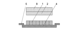
- the adhesive tape 4 is bonded to the divided chip surface as the semiconductor member 1 through the ring frame 5 using a roll mounter. The state after the bonding step is shown in FIG.
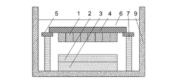
- the adhesive resin 2 and the fixing jig 3 were freely dropped from the semiconductor member 1 and peeled off after being immersed in warm water 6 at 90 ° C. in the state after the bonding step.
- FIG. 3 shows the immersed state
- FIG. 4 shows the state after free fall.
- reference numeral 7 denotes a column supporting the ring frame 5
- reference numeral 9 denotes a container containing hot water 6.
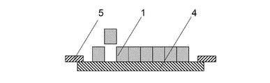
- the pressure-sensitive adhesive tape 4 bonded to the ring frame 5 is pulled up together with the semiconductor member 1 (see FIG. 5), and the high-pressure mercury lamp manufactured by USHIO INC. From the base film side of the pressure-sensitive adhesive tape 4 (lower side in FIG. 5). After irradiating with ultraviolet rays under the condition of 150 mJ / cm 2 and curing the adhesive layer of the adhesive tape 4, using CAP-300II manufactured by Canon Machinery not shown in the figure, under the condition of needle pin height 0.3 mm. It was. The state at the time of pick-up is shown in FIG.
- FIG. 7 is a schematic cross-sectional view showing a transfer step when a peeling tape is used.
- This method has the same configuration as the above-described method except that the semiconductor member 1 is changed to a silicon wafer having a polyimide vapor deposition film (not shown) formed on its surface (contact surface with the adhesive resin 2).
- a silicon wafer having a polyimide vapor deposition film formed on the surface of the semiconductor member 1 (contact surface with the adhesive resin 2) is formed, the interface between the semiconductor member 1 and the adhesive tape 4 and the adhesive resin in the transfer process. 2 and the fixing jig 3, not the interface between the adhesive resin 2 and the fixing jig 3.
- the peeling tape 8 is attached to the surface of the adhesive resin 2 (see FIG. 9) from the state where it is pulled up from the hot water 6 shown in FIG. 8, and the peeling tape 8 is peeled off together with the adhesive resin 2 (FIG. 10). reference).
- the subsequent steps are as shown in FIGS.
- Substrate A Propylene copolymer (containing propylene, ethylene, 1-butene as a polymerization component, MFR (melt flow rate) value 7.5 g / 10 min, density 0.89 g / cm 3 (manufactured by Sun Allomer, X500F )). 80 ⁇ m thick.
- Base material B random copolymer of ethylene and vinyl acetate (MFR value 2.5 g / 10 min, vinyl acetate content 12%, density 0.93 g / cm 3 (manufactured by Mitsui DuPont Polychemical Co., Ltd.), thickness 80 ⁇ m.
- Substrate C PET, thickness 38 ⁇ m.
- (Adhesive for adhesive tape) The following was adopted as the adhesive.
- the numbers in Table 1 are parts by mass.
- (Meth) acrylic acid ester copolymer made of a copolymer of 54% ethyl acrylate, 19% butyl acrylate and 24% methoxyethyl acrylate, obtained by emulsion polymerization (our polymer).
- Multifunctional isocyanate curing agent Commercial product of trimethylolpropane adduct of hexamethylene diisocyanate (product name: Coronate HL, manufactured by Nippon Polyurethane Co., Ltd.).
- Urethane acrylate oligomer A terminal acrylate oligomer obtained by further reacting dipetaerythritol pentaacrylate with terminal isocyanate oligomer obtained by reacting hexamethylene diisocyanate (aliphatic diisocyanate) trimer to the terminal of poly (propylene oxide) diol
- Urethane acrylate oligomer B a terminal acrylate oligomer obtained by further reacting 2-hydroxyethyl acrylate with a terminal isocyanate oligomer obtained by reacting 2-hydroxyethyl acrylate with an end of poly (propylene oxide) diol, and having a number average molecular weight (Mn) is 3,400 and the number of vinyl groups is 2 urethane acrylate oligomers per molecule (our polymerized product).
- Silicon-modified acrylic resin A commercial product of a silicon-based graft copolymer obtained by polymerizing an acrylic vinyl unit composed of a silicon-based oligomer having a (meth) acryloyl group at the end of a silicon molecular chain and methyl methacrylate (Soken Chemical Co., Ltd.) Product name Actflow UTMM-LS2).
- Experiment No. 1 pressure-sensitive adhesive is 100 parts by weight of (meth) acrylic acid ester copolymer A, 3 parts by weight of polyfunctional isocyanate curing agent A, 100 parts by weight of urethane acrylate oligomer A, 2 parts by weight of silicon-modified acrylic resin A, and 6 parts by weight of photopolymerization initiator. Are blended.
- the adhesive tape is obtained by applying an adhesive having the composition shown in Table 1 on a PET separator film, applying the adhesive layer so that the thickness of the adhesive layer after drying is 10 ⁇ m, and laminating it on a substrate.
- the adhesive resin used was a blend of (A) polyfunctional (meth) acrylate, (B) monofunctional (meth) acrylate and (C) polymerization initiator.
- A) polyfunctional (meth) acrylate 8 parts by mass of urethane acrylate (“UV-3000B” manufactured by Nippon Synthetic Chemical Co., Ltd.), dicyclopentanyl diacrylate (“KAYARAD R— manufactured by Nippon Kayaku Co., Ltd.) 684 ") 20 parts by mass in total of 12 parts by mass
- Base material A random copolymer of ethylene and vinyl acetate (MFR value 2.5 g / 10 min, vinyl acetate content 12%, density 0.93 g / cm 3 , manufactured by Mitsui DuPont Polychemical Co., Ltd.) is formed to a thickness of 100 ⁇ m. We adopted what we did.
- Adhesive Blended with the following ingredients, this adhesive was coated on a PET separator film, coated so that the thickness of the adhesive layer after drying was 20 ⁇ m, and laminated on the substrate thing.
- (Combination material) The following materials were used as the material for the peeling tape.
- the semiconductor member manufacturing method according to the present invention was implemented and evaluated for the semiconductor member (silicon wafer) by the above-described method.
- the evaluation results are shown in Table 1.
- the peeling tape was used, and the adhesive resin was peeled from the separated semiconductor member.
- An adhesive resin was applied to a silicon wafer having a diameter of 8 inches and a thickness of 725 ⁇ m by spin coating, a glass plate having a thickness of 700 ⁇ m was bonded thereto, and 10 kg was applied so that a uniform surface could be obtained. Thereafter, the adhesive resin was cured using a black light under a condition of 300 mJ / cm 2 at a wavelength of 365 nm.
- Dicing is performed with a DAD341 manufactured by DISCO and NBC-ZH205O-27HEEE manufactured by DISCO, with a chip size of 7.2 mm ⁇ 14.4 mm, and a wavelength of 365 nm by a curing device manufactured by Fusion using an electrodeless discharge lamp.
- the adhesive resin under the conditions of 16000 mJ / cm 2 , using a roll mounter, the adhesive tape is bonded to the divided chip surface via a ring frame, and the semiconductor member is faced downward to a liquid at 90 ° C. Then, the adhesive resin and glass were freely dropped from the fixing jig and separated from the semiconductor member.
- Experiment No. No. 2 was immersed with the semiconductor member facing upward.
- the case where the chip was able to be peeled from the adhesive resin and glass within 1 minute at the time of peeling was rated as ⁇ , the case where the chip was peeled off within 30 minutes was marked as ⁇ , and the case where the chip could not be peeled off after 30 minutes was marked as x.
- the semiconductor member is immersed downward in a liquid at 90 ° C, if only the glass peels from the semiconductor member and the adhesive resin adheres to the semiconductor member, after drying, peel off the adhesive resin and attach the tape. Then, the tape was peeled off from the separated semiconductor member together with the adhesive resin.
- the distance between the chips transferred by the above method was measured in one row each in the vertical direction and the horizontal direction, and compared with the chip distance before transfer.
- ⁇ is 10 ⁇ m or more and less than 20 ⁇ m
- ⁇ is 20 ⁇ m or more.
- UV light is irradiated from the base film surface of the adhesive tape with a high pressure mercury lamp manufactured by USHIO INC. Under the condition of 150 mJ / cm 2 to cure the adhesive layer, and then CAP manufactured by Canon Machinery. -300II was evaluated under the condition of a needle pin height of 0.3 mm. A case where 100% of the chip was picked up was marked as ⁇ , a case where it was 90% or more and less than 100% was marked as ⁇ , and a case where it was less than 90% was marked as ⁇ .
Landscapes
- Chemical & Material Sciences (AREA)
- Organic Chemistry (AREA)
- Health & Medical Sciences (AREA)
- Chemical Kinetics & Catalysis (AREA)
- Medicinal Chemistry (AREA)
- Polymers & Plastics (AREA)
- Adhesive Tapes (AREA)
- Adhesives Or Adhesive Processes (AREA)
- Dicing (AREA)
Abstract
半導体部材に接着性樹脂を塗布し、半導体部材を、接着性樹脂を介して固定用冶具に仮固定し、個片化する個片化工程と、個片化された半導体部材に粘着テープを貼り合わせる貼合工程と、接着性樹脂の接着力低下温度Xと、粘着テープの熱収縮温度Yの間の温度域の液体に浸漬させ、個片化された半導体部材から接着性樹脂及び固定用冶具を剥離し、半導体部材を粘着テープに転写する転写工程と、粘着テープ上の個片化された半導体部材をピックアップするピックアップ工程と、を含む半導体部材製造方法。
Description
本発明は、半導体部材製造方法とこれら方法に用いる粘着テープに関する。
一般的に、IC(Integrated Circuit)カード、携帯電話、及びPDA(Personal Digital Assistants)等の電子機器は、回路パターンを形成したチップ状の電子部品を搭載している。
半導体部材は、シリコン又はガリウム-砒素等の半導体ウエハ、絶縁基板等に複数の回路パターンを形成した半導体部材を個々に分割することによって形成されるものであり、電子機器の薄型化により、電子部品も薄型化が進んでいる(特許文献1参照)。
しかし、薄くなった半導体部材を、ダイヤモンド砥粒を有するダイシングブレードにより個片化した場合、半導体部材の割れ等が生じる場合があった。
本発明によれば、半導体部材に接着性樹脂を塗布し、半導体部材を、接着性樹脂を介して固定用冶具に仮固定し、個片化する個片化工程と、個片化された半導体部材に粘着テープを貼り合わせる貼合工程と、接着性樹脂の接着力低下温度Xと、粘着テープの熱収縮温度Yの間の温度域の液体に浸漬させ、個片化された半導体部材から接着性樹脂及び固定用冶具を剥離し、半導体部材を粘着テープに転写する転写工程と、粘着テープ上の個片化された半導体部材をピックアップするピックアップ工程と、を含む半導体部材製造方法が提供される。
また、本発明によれば、半導体部材に接着性樹脂を塗布し、半導体部材を、接着性樹脂を介して固定用冶具に仮固定し、個片化する個片化工程と、個片化された半導体部材に粘着テープを貼り合わせる貼合工程と、接着性樹脂の接着力低下温度Xと、粘着テープの熱収縮温度Yの間の温度域の液体に浸漬させ、接着性樹脂から固定用冶具を剥離し、半導体部材を粘着テープに転写する転写工程と、接着性樹脂に剥がしテープを貼り合わせる第二貼合工程と、個片化された半導体部材から剥がしテープを接着性樹脂ごと剥離する第二剥離工程と、粘着テープ上の個片化された半導体部材をピックアップするピックアップ工程と、を含む半導体部材製造方法が提供される。
上記構成からなる半導体製造方法によれば、剥離性、転写性及びピックアップ性に優れた半導体部材製造方法を提供できる。
本発明の一態様によれば、転写工程で用いる液体の温度が40℃以上100℃以下である。
また、本発明の一態様によれば、転写工程において、半導体部材の粘着テープが貼り付けられた側を上方にし、半導体部材の接着性樹脂及び固定用冶具が貼り付けられた側を下方にして液体に浸漬させる。また、転写工程において、半導体部材を粘着テープを介して液体中に浮かせることによって、固定用冶具を接着性樹脂ごと自由落下させる。
また、本発明の一態様によれば、転写工程において、半導体部材の粘着テープが貼り付けられた側を上方にし、半導体部材の接着性樹脂及び固定用冶具が貼り付けられた側を下方にして液体に浸漬させる。また、転写工程において、半導体部材を粘着テープを介して液体中に浮かせることによって、固定用冶具を接着性樹脂ごと自由落下させる。
また、本発明の一態様によれば、粘着テープの基材フィルムが、プロピレン系共重合体である。
本発明の一態様によれば、粘着テープの粘着剤層が、(メタ)アクリル酸エステル共重合体100質量部、多官能イソシアネート系硬化剤0.5質量部以上20質量部以下、ビニル基を4個以上有するウレタンアクリレートオリゴマ20質量部以上200質量部以下、及びシリコン変性アクリル樹脂0.1質量部以上10質量部以下、を含有することを特徴とする請求項1ないし6のいずれか記載の半導体部材製造方法。
本発明の一態様によれば、粘着テープの粘着剤層が、(メタ)アクリル酸エステル共重合体100質量部、多官能イソシアネート系硬化剤0.5質量部以上20質量部以下、ビニル基を4個以上有するウレタンアクリレートオリゴマ20質量部以上200質量部以下、及びシリコン変性アクリル樹脂0.1質量部以上10質量部以下、を含有することを特徴とする請求項1ないし6のいずれか記載の半導体部材製造方法。
本発明によれば、剥離性、転写性及びピックアップ性に優れた半導体部材製造方法を提供できる。
1 個片化された半導体部材
2 接着性樹脂
3 固定用冶具
4 粘着テープ
5 リングフレーム
6 温水
7 支柱
8 剥がしテープ
9 容器
2 接着性樹脂
3 固定用冶具
4 粘着テープ
5 リングフレーム
6 温水
7 支柱
8 剥がしテープ
9 容器
以下、本発明にかかる半導体部材製造方法の実施形態とこの方法に用いる粘着テープの実施形態について詳細に説明するが、本発明がこれらの実施形態に限定される趣旨でないことは自明である。
本実施形態にかかる半導体部材製造方法は、半導体部材に接着性樹脂を塗布し、半導体部材を、接着性樹脂を介して固定用冶具に仮固定し、個片化する個片化工程と、個片化された半導体部材に粘着テープを貼り合わせる貼合工程と、接着性樹脂の接着力低下温度Xと、粘着テープの熱収縮温度Yの間の温度域の液体に浸漬させ、個片化された半導体部材から接着性樹脂及び固定用冶具を剥離し、半導体部材を粘着テープに転写する転写工程と、粘着テープ上の個片化された半導体部材をピックアップするピックアップ工程と、を含む半導体部材製造方法である。
<個片化工程>
半導体部材に接着性樹脂を塗布し、半導体部材を、接着性樹脂を介して固定用冶具に仮固定し、個片化する個片化工程で用いられる半導体部材としては、円板状のシリコンウエハ、ガラス、ガリウム-砒素(GaAs)がある。
接着性樹脂としては、アクリル系樹脂、エポキシ系樹脂が好ましく用いられる。固定用冶具としては、ガラス、セラミックがある。
半導体部材に接着性樹脂を塗布し、半導体部材を、接着性樹脂を介して固定用冶具に仮固定し、個片化する個片化工程で用いられる半導体部材としては、円板状のシリコンウエハ、ガラス、ガリウム-砒素(GaAs)がある。
接着性樹脂としては、アクリル系樹脂、エポキシ系樹脂が好ましく用いられる。固定用冶具としては、ガラス、セラミックがある。
半導体部材を個片化する方法としては、ダイヤモンド砥粒を有するダイシングブレードによる切断、エッチング等がある。
<貼合工程>
個片化された半導体部材に粘着テープを貼り合わせる貼合工程は、例えば、個片化されたが接着性樹脂により全体的に円板状を維持した半導体部材の接着性樹脂が積層されていない面に粘着テープを貼る工程であり、貼り合わせる方法は、例えばロール圧着、真空圧着がある。
個片化された半導体部材に粘着テープを貼り合わせる貼合工程は、例えば、個片化されたが接着性樹脂により全体的に円板状を維持した半導体部材の接着性樹脂が積層されていない面に粘着テープを貼る工程であり、貼り合わせる方法は、例えばロール圧着、真空圧着がある。
<転写工程>
接着性樹脂の接着力低下温度Xと、粘着テープの熱収縮温度Yの間の温度域の液体に浸漬させ、個片化された半導体部材から接着性樹脂及び固定用冶具を剥離し、半導体部材を粘着テープに転写する転写工程は、具体的には、接着性樹脂と固定用冶具を半導体部材から剥離することによって、半導体部材が粘着テープに転写することをいう。この剥離の方法としては、転写工程が接着性樹脂の接着力低下温度Xと、粘着テープの熱収縮温度Yの間の温度域の液体に浸漬させることによって達成できる。
接着性樹脂の接着力低下温度Xと、粘着テープの熱収縮温度Yの間の温度域の液体に浸漬させ、個片化された半導体部材から接着性樹脂及び固定用冶具を剥離し、半導体部材を粘着テープに転写する転写工程は、具体的には、接着性樹脂と固定用冶具を半導体部材から剥離することによって、半導体部材が粘着テープに転写することをいう。この剥離の方法としては、転写工程が接着性樹脂の接着力低下温度Xと、粘着テープの熱収縮温度Yの間の温度域の液体に浸漬させることによって達成できる。
接着性樹脂の接着力低下温度Xと、粘着テープの熱収縮温度Yは、X<Yの関係が必要であり、液体の温度Tは、X<T<Yの関係であることが必要である。接着力低下温度は、接着性樹脂と粘着テープの基材フィルムとして採用する合成樹脂に応じて異なり、液体の温度Tの設定値の下限が低いと接着性樹脂の接着力低下が生じにくい傾向にあり、設定値の上限が高いと粘着テープが収縮してしまう傾向にある。
この液体の設定温度としては、具体的には、下限としては40℃、好ましくは75℃であり、上限としては120℃、好ましくは100℃である。液体としては、水、油があるが、半導体部材への影響を考えると水が好ましい。
この液体の設定温度としては、具体的には、下限としては40℃、好ましくは75℃であり、上限としては120℃、好ましくは100℃である。液体としては、水、油があるが、半導体部材への影響を考えると水が好ましい。
転写工程において、上から粘着テープ、半導体部材、接着性樹脂、固定用冶具という配置にして液体に浸漬させることが好ましい。即ち、転写工程において、半導体部材の粘着テープが貼り付けられた側を上方にし、半導体部材の接着性樹脂及び固定用冶具が貼り付けられた側を下方にして液体に浸漬させることが好ましい。
この配置のまま浸漬させることにより、接着性樹脂は固定冶具との自重と接着性樹脂の粘着力の低下によって剥離させることができる。この配置による剥離を採用することによって、自重による自由落下なため、接着性樹脂付きの固定用冶具剥離時の負荷を抑制し、粘着テープへ個片化された半導体部材を移し替える際の個片化された半導体部材同士の間隔を変動させることなく、液体への浸漬時の個片化された半導体部材の割れ、欠けを防止することができるとともに、接着性樹脂への液体の浸透を促進し、転写時間を短縮することができた。
この配置のまま浸漬させることにより、接着性樹脂は固定冶具との自重と接着性樹脂の粘着力の低下によって剥離させることができる。この配置による剥離を採用することによって、自重による自由落下なため、接着性樹脂付きの固定用冶具剥離時の負荷を抑制し、粘着テープへ個片化された半導体部材を移し替える際の個片化された半導体部材同士の間隔を変動させることなく、液体への浸漬時の個片化された半導体部材の割れ、欠けを防止することができるとともに、接着性樹脂への液体の浸透を促進し、転写時間を短縮することができた。
接着性樹脂の接着力によっては、転写工程での剥離界面は、半導体部材・接着性樹脂間、又は接着性樹脂・固定用冶具間の2種類がある。後者の場合、接着性樹脂に剥がしテープを貼り合わせ、個片化された半導体部材から剥がしテープを接着性樹脂ごと剥離する。
(粘着テープ)
粘着テープは、基材と粘着剤層から構成され、接着性樹脂の粘着力低下温度より高い粘着力低下温度を有する粘着剤が積層されたものである。
粘着テープは、基材と粘着剤層から構成され、接着性樹脂の粘着力低下温度より高い粘着力低下温度を有する粘着剤が積層されたものである。
(粘着テープの基材)
粘着テープの基材としては、浸漬されても膨張、収縮等の変形をしない材料が好ましく、合成樹脂、金属がよい。基材の形状としてはフィルム、シート、箔がある。
基材の厚みは、50μm以上250μm以下が良い。より好ましい下限は70μmであり、より好ましい上限は150μmである。基材の厚みが薄くなるとピックアップ工程におけるエキスパンド時に基材の切断が生じる傾向にあり、基材の厚みが厚くなるとエキスパンド性に劣る傾向にある。
粘着テープの基材としては、浸漬されても膨張、収縮等の変形をしない材料が好ましく、合成樹脂、金属がよい。基材の形状としてはフィルム、シート、箔がある。
基材の厚みは、50μm以上250μm以下が良い。より好ましい下限は70μmであり、より好ましい上限は150μmである。基材の厚みが薄くなるとピックアップ工程におけるエキスパンド時に基材の切断が生じる傾向にあり、基材の厚みが厚くなるとエキスパンド性に劣る傾向にある。
粘着テープの基材として用いられる合成樹脂としては、PVC(ポリ塩化ビニル)、ポリエチレン、PET(ポリエチレンテレフタレート)、EVA(エチレン-酢酸ビニル共重合体)、エチレン-エチルアクリレート共重合体、ポリプロピレン、プロピレン系共重合体、エチレン-アクリル酸共重合体、アイオノマ樹脂、ポリイミドがあり、この中で、PET、プロピレン系共重合体が好ましく、プロピレン系共重合体が更に好ましい。
粘着テープの基材として用いられる金属としては、ステンレス、銅、アルミニウムがある。基材として、これら合成樹脂の混合物、共重合体、合成樹脂同士の積層体、金属同士の積層体、合成樹脂と金属の積層体であってもよい。
粘着テープの基材として用いられる金属としては、ステンレス、銅、アルミニウムがある。基材として、これら合成樹脂の混合物、共重合体、合成樹脂同士の積層体、金属同士の積層体、合成樹脂と金属の積層体であってもよい。
基材としてプロピレン系共重合体を選択した場合、浸漬時の変形がなく、剥離時の半導体部材の変動が生じないと共に、次のピックアップ工程において、より良好なピックアップ性を得られるためである。
このプロピレン系共重合体としては、例えばプロピレンと他成分とのランダム共重合体、プロピレンと他成分とのブロック共重合体、プロピレンと他成分の交互共重合体がある。他成分としては、エチレン、1-ブテン、1-ペンテン、1-ヘキセン、1-ヘプテン等のα-オレフィン、少なくとも2種以上のα-オレフィンからなる共重合体、スチレン-ジエン共重合体等が挙げられる。これらの中でも1-ブテンが好ましい。これにより、半導体部材を切断する際に発生する切り屑を特に抑制することができる。
このプロピレン系共重合体としては、例えばプロピレンと他成分とのランダム共重合体、プロピレンと他成分とのブロック共重合体、プロピレンと他成分の交互共重合体がある。他成分としては、エチレン、1-ブテン、1-ペンテン、1-ヘキセン、1-ヘプテン等のα-オレフィン、少なくとも2種以上のα-オレフィンからなる共重合体、スチレン-ジエン共重合体等が挙げられる。これらの中でも1-ブテンが好ましい。これにより、半導体部材を切断する際に発生する切り屑を特に抑制することができる。
(粘着テープの粘着剤)
粘着テープの粘着剤としては、アクリル酸、メタクリル酸及びそれらのエステルモノマーを重合させたポリマー、これらモノマーと共重合可能な不飽和単量体(例えば、酢酸ビニル、スチレン、アクリロニトリル)とを共重合させたコポリマーがあり、これら粘着剤のうち、(メタ)アクリル酸エステル共重合体が好ましい。
粘着剤層には、紫外線又は放射線の照射によって三次元網状化しうる分子内に光重合性炭素-炭素二重結合を分子内に少なくとも2個以上有する低分子量化合物、例えばアクリレート化合物又はウレタンアクリレートオリゴマ等を用いた光硬化型感圧性粘着剤も採用できる。
粘着テープの粘着剤としては、アクリル酸、メタクリル酸及びそれらのエステルモノマーを重合させたポリマー、これらモノマーと共重合可能な不飽和単量体(例えば、酢酸ビニル、スチレン、アクリロニトリル)とを共重合させたコポリマーがあり、これら粘着剤のうち、(メタ)アクリル酸エステル共重合体が好ましい。
粘着剤層には、紫外線又は放射線の照射によって三次元網状化しうる分子内に光重合性炭素-炭素二重結合を分子内に少なくとも2個以上有する低分子量化合物、例えばアクリレート化合物又はウレタンアクリレートオリゴマ等を用いた光硬化型感圧性粘着剤も採用できる。
((メタ)アクリル酸エステル共重合体)
粘着テープの粘着剤として用いられる(メタ)アクリル酸エステル共重合体は、特に限定されないが、(メタ)アクリル酸エステルの主単量体と、その他のビニル化合物単量体を共重合したものである。ビニル化合物単量体は、ヒドロキシル基、カルボキシル基、エポキシ基、アミド基、アミノ基、メチロール基、スルホン酸基、スルファミン酸基、及び(亜)リン酸エステル基からなる官能基群の1種以上を有する官能基含有単量体を用いることが好ましい。
粘着テープの粘着剤として用いられる(メタ)アクリル酸エステル共重合体は、特に限定されないが、(メタ)アクリル酸エステルの主単量体と、その他のビニル化合物単量体を共重合したものである。ビニル化合物単量体は、ヒドロキシル基、カルボキシル基、エポキシ基、アミド基、アミノ基、メチロール基、スルホン酸基、スルファミン酸基、及び(亜)リン酸エステル基からなる官能基群の1種以上を有する官能基含有単量体を用いることが好ましい。
(メタ)アクリル酸エステルの主単量体としては、例えばブチル(メタ)アクリレート、2-ブチル(メタ)アクリレート、t-ブチル(メタ)アクリレート、ペンチル(メタ)アクリレート、オクチル(メタ)アクリレート、2-エチルヘキシル(メタ)アクリレート、ノニル(メタ)アクリレート、デシル(メタ)アクリレート、ラウリル(メタ)アクリレート、メチル(メタ)アクリレート、エチル(メタ)アクリレート、イソプロピル(メタ)アクリレート、トリデシル(メタ)アクリレート、ミリスチル(メタ)アクリレート、セチル(メタ)アクリレート、ステアリル(メタ)アクリレート、シクロヘキシル(メタ)アクリレート、イソボロニル(メタ)アクリレート、ジシクロペンタニル(メタ)アクリレート、ベンジル(メタ)アクリレート、メトキシエチル(メタ)アクリレート、エトキシエチル(メタ)アクリレート、ブトキシメチル(メタ)アクリレート、及びエトキシ-n-プロピル(メタ)アクリレート等が挙げられる。
官能基含有単量体としては、例えば官能基としてヒドロキシル基、カルボキシル基、エポキシ基、アミド基、アミノ基、メチロール基、スルホン酸基、スルファミン酸基、(亜)リン酸エステル基を有するビニル化合物が挙げられる。
ヒドロキシル基を有する単量体としては、例えば2-ヒドロキシエチル(メタ)アクリレート、2-ヒドロキシプロピル(メタ)アクリレート、及び2-ヒドロキシブチル(メタ)アクリレート等が挙げられる。
カルボキシル基を有する単量体としては、例えば(メタ)アクリル酸、クロトン酸、マレイン酸、無水マレイン酸、イタコン酸、フマル酸、アクリルアミドN-グリコール酸、及びケイ皮酸等が挙げられる。
カルボキシル基を有する単量体としては、例えば(メタ)アクリル酸、クロトン酸、マレイン酸、無水マレイン酸、イタコン酸、フマル酸、アクリルアミドN-グリコール酸、及びケイ皮酸等が挙げられる。
エポキシ基を有する単量体としては、例えばアリルグリシジルエーテル、及び(メタ)アクリル酸グリシジルエーテル等が挙げられる。
アミド基を有する単量体としては、例えば(メタ)アクリルアミド等が挙げられる。
アミド基を有する単量体としては、例えば(メタ)アクリルアミド等が挙げられる。
アミノ基を有する単量体としては、例えばN,N-ジメチルアミノエチル(メタ)アクリレート等が挙げられる。
メチロール基を有する単量体としては、例えばN-メチロールアクリルアミド等が挙げられる。
メチロール基を有する単量体としては、例えばN-メチロールアクリルアミド等が挙げられる。
(メタ)アクリル酸エステル共重合体の製造方法は、乳化重合、溶液重合等の公知の方法が使用できる。放射線照射後に粘着テープが半導体部材と容易に剥離できるように、乳化重合により製造できるアクリルゴムが好ましい。
(多官能イソシアネート硬化剤)
粘着テープの粘着剤として用いられる多官能イソシアネート硬化剤はイソシアネート基を2個以上有する点以外に特に限定されず、例えば芳香族ポリイソシアネート、脂肪族ポリイソシアネート、脂環族ポリイソシアネート等が挙げられる。
粘着テープの粘着剤として用いられる多官能イソシアネート硬化剤はイソシアネート基を2個以上有する点以外に特に限定されず、例えば芳香族ポリイソシアネート、脂肪族ポリイソシアネート、脂環族ポリイソシアネート等が挙げられる。
芳香族ポリイソシアネートは特に限定されず、例えば1,3-フェニレンジイソシアネート、4,4’-ジフェニルジイソシアネート、1,4-フェニレンジイソシアネート、4,4’-ジフェニルメタンジイソシアネート、2,4-トリレンジイソシアネート、2,6-トリレンジイソシアネート、4,4’-トルイジンジイソシアネート、2,4,6-トリイソシアネートトルエン、1,3,5-トリイソシアネートベンゼン、ジアニシジンジイソシアネート、4,4’-ジフェニルエーテルジイソシアネート、4,4’,4”-トリフェニルメタントリイソシアネート、ω,ω’-ジイソシアネート-1,3-ジメチルベンゼン、ω,ω’-ジイソシアネート-1,4-ジメチルベンゼン、ω,ω’-ジイソシアネート-1,4-ジエチルベンゼン、1,4-テトラメチルキシリレンジイソシアネート、及び1,3-テトラメチルキシリレンジイソシアネート等が挙げられる。
脂肪族ポリイソシアネートは特に限定されず、例えばトリメチレンジイソシアネート、テトラメチレンジイソシアネート、ヘキサメチレンジイソシアネート、ペンタメチレンジイソシアネート、1,2-プロピレンジイソシアネート、2,3-ブチレンジイソシアネート、1,3-ブチレンジイソシアネート、ドデカメチレンジイソシアネート、及び2,4,4-トリメチルヘキサメチレンジイソシアネート等が挙げられる。
脂環族ポリイソシアネートは特に限定されず、例えば3-イソシアネートメチル-3,5,5-トリメチルシクロヘキシルイソシアネート、1,3-シクロペンタンジイソシアネート、1,3-シクロヘキサンジイソシアネート、1,4-シクロヘキサンジイソシアネート、メチル-2,4-シクロヘキサンジイソシアネート、メチル-2,6-シクロヘキサンジイソシアネート、4,4’-メチレンビス(シクロヘキシルイソシアネート)、1,4-ビス(イソシアネートメチル)シクロヘキサン、及び1,4-ビス(イソシアネートメチル)シクロヘキサン等が挙げられる。
ポリイソシアネートのうち、1,3-フェニレンジイソシアネート、4,4’-ジフェニルジイソシアネート、1,4-フェニレンジイソシアネート、4,4’-ジフェニルメタンジイソシアネート、2,4-トリレンジイソシアネート、2,6-トリレンジイソシアネート、4,4’-トルイジンジイソシアネート、ヘキサメチレンジイソシアネートが好適に用いられる。
多官能イソシアネート硬化剤の配合比は((メタ)アクリル酸エステル共重合体)100質量部に対して0.1質量部以上20質量部以下が好ましく、下限としては0.5質量部、上限としては10質量部がより好ましい。
多官能イソシアネート硬化剤が0.1質量部以上であれば、粘着力が強すぎないので、ピックアップ不良の発生を抑制することができる。また、多官能イソシアネート硬化剤が20質量部以下であれば、粘着力が低下せず、液体浸漬時の転写工程における個片化された半導体部材の保持性が維持されるので好ましい。
多官能イソシアネート硬化剤が0.1質量部以上であれば、粘着力が強すぎないので、ピックアップ不良の発生を抑制することができる。また、多官能イソシアネート硬化剤が20質量部以下であれば、粘着力が低下せず、液体浸漬時の転写工程における個片化された半導体部材の保持性が維持されるので好ましい。
(ビニル基を4個以上有するウレタンアクリレートオリゴマ)
粘着テープの粘着剤として用いられる、ビニル基を4個以上有するウレタンアクリレートオリゴマ(以下、単に「ウレタンアクリレートオリゴマ」という。)とは、ビニル基を4個以上有し、分子内にウレタン結合を有する(メタ)アクリレートオリゴマーであれば特に限定されない。
粘着テープの粘着剤として用いられる、ビニル基を4個以上有するウレタンアクリレートオリゴマ(以下、単に「ウレタンアクリレートオリゴマ」という。)とは、ビニル基を4個以上有し、分子内にウレタン結合を有する(メタ)アクリレートオリゴマーであれば特に限定されない。
ウレタンアクリレートオリゴマの製造方法は特に限定されないが、例えば水酸基と複数の(メタ)アクリレート基を含有する(メタ)アクリレート化合物と、複数のイソシアネート基を有する化合物(例えばジイソシアネート化合物)を反応させてウレタンアクリレートオリゴマとする方法が挙げられる。複数の水酸基末端を有するポリオールオリゴマに、複数のイソシアネート基を有する化合物(例えばジイソシアネート化合物)を過剰に添加して反応させて複数のイソシアネート末端を有するオリゴマーとし、更に水酸基と複数の(メタ)アクリレート基を含有する(メタ)アクリレート化合物と反応させてウレタンアクリレートオリゴマとしてもよい。
水酸基と複数の(メタ)アクリレート基を含有する(メタ)アクリレート化合物としては、例えば、ヒドロキシプロピル化トリメチロールプロパントリアクリレート、ペンタエリスリトールトリアクリレート、ジペンタエリスリトール-ヒドロキシ-ペンタアクリレート、ビス(ペンタエリスリトール)-テトラアクリレート、テトラメチロールメタン-トリアクリレート、グリシドール-ジアクリレートや、これらのアクリレート基の一部又は全部をメタアクリレート基とした化合物等が挙げられる。
複数のイソシアネート基を有するイソシアネートとしては、例えば、芳香族イソシアネート、脂環族イソシアネート、及び脂肪族イソシアネート等が挙げられる。これらのイソシアネートのうち、複数のイソシアネート基を有する、芳香族イソシアネート又は脂環族イソシアネートが好適に用いられる。イソシアネート成分の形態としては単量体、二量体、三量体があり、三量体が好適に用いられる。
芳香族ジイソシアネートとしては、例えば、トリレンジイソシアネート、4,4-ジフェニルメタンジイソシアネート、キシリレンジイソシアネートなどがある。
脂環族ジイソシアネートとしては、例えば、イソホロンジイソシアネート、メチレンビス(4-シクロヘキシルイソシアネート)などが挙げられる。
脂肪ジイソシアネートとしては、例えば、ヘキサメチレンジイソシアネート、トリメチルヘキサメチレンジイソシアネート等が挙げられる。
脂肪ジイソシアネートとしては、例えば、ヘキサメチレンジイソシアネート、トリメチルヘキサメチレンジイソシアネート等が挙げられる。
ポリオール成分としては、例えば、ポリ(プロピレンオキサイド)ジオール、ポリ(プロピレンオキサイド)トリオール、コポリ(エチレンオキサイド-プロピレンオキサイド)ジオール、ポリ(テトラメチレンオキサイド)ジオール、エトキシ化ビスフェノールA、エトキシ化ビスフェノールSスピログリコール、カプロラクトン変性ジオール、カーボネートジオール等が挙げられる。
ビニル基を有するウレタンアクリレートオリゴマのビニル基の数が4個以上であれば、放射線照射後の粘着テープの半導体部材からの剥離が容易なので、ピックアップ性を向上させることができる。
ビニル基を4個以上有するウレタンアクリレートオリゴマの配合量は特に限定されないが、(メタ)アクリル酸エステル共重合体100質量部に対して20質量部以上200質量部以下とすることが好ましい。ビニル基を4個以上有するウレタンアクリレートオリゴマの配合量が20質量部以上であれば、放射線照射後の粘着テープの半導体部材からの剥離が容易となり、ピックアップ性の問題の発生を抑制することができる。
また、ビニル基を4個以上有するウレタンアクリレートオリゴマの配合量が200質量部以下であれば、液体への浸漬時の転写工程における個片化された半導体部材の保持性が維持されることができる。
また、ビニル基を4個以上有するウレタンアクリレートオリゴマの配合量が200質量部以下であれば、液体への浸漬時の転写工程における個片化された半導体部材の保持性が維持されることができる。
(シリコン変性アクリル樹脂)
粘着テープの粘着剤として用いられるシリコン変性アクリル樹脂は、(メタ)アクリル単量体とポリジメチルシロキサン結合の末端にビニル基を有する単量体(以下、「シリコン系マクロモノマ」という)の重合物であり、ポリジメチルシロキサン結合の末端にビニル基を有する単量体に由来する単量体単位を有する点以外は特に限定されず、例えばシリコン系マクロモノマのホモポリマーや、シリコン系マクロモノマと他のビニル化合物を重合してなるビニル重合体が挙げられる。
シリコン系マクロモノマは、ポリジメチルシロキサン結合の末端が(メタ)アクリロイル基またはスチリル基等のビニル基となっている化合物が好適に用いられる(例えば、特開2000-080135号公報等参照)。
粘着テープの粘着剤として用いられるシリコン変性アクリル樹脂は、(メタ)アクリル単量体とポリジメチルシロキサン結合の末端にビニル基を有する単量体(以下、「シリコン系マクロモノマ」という)の重合物であり、ポリジメチルシロキサン結合の末端にビニル基を有する単量体に由来する単量体単位を有する点以外は特に限定されず、例えばシリコン系マクロモノマのホモポリマーや、シリコン系マクロモノマと他のビニル化合物を重合してなるビニル重合体が挙げられる。
シリコン系マクロモノマは、ポリジメチルシロキサン結合の末端が(メタ)アクリロイル基またはスチリル基等のビニル基となっている化合物が好適に用いられる(例えば、特開2000-080135号公報等参照)。
(メタ)アクリル単量体としては、アルキル(メタ)アクリレートの他に、ヒドロキシアルキル(メタ)アクリレート、変性ヒドロキシ(メタ)アクリレート、及び(メタ)アクリル酸等が挙げられる。
アルキル(メタ)アクリレートとしては、例えばメチル(メタ)アクリレート、エチル(メタ)アクリレート、n-プロピル(メタ)アクリレート、n-ブチル(メタ)アクリレート、イソブチル(メタ)アクリレート、t-ブチル(メタ)アクリレート、2-エチルヘキシル(メタ)アクリレート、ラウリル(メタ)アクリレート、ステアリル(メタ)アクリレート、及びイソボルニル(メタ)アクリレート、及びヒドロキシアルキル(メタ)アクリレート等が挙げられる。
ヒドロキシアルキル(メタ)アクリレートとしては、例えばヒドロキシエチル(メタ)アクリレート、ヒドロキシプロピル(メタ)アクリレート、及びヒドロキシブチル(メタ)アクリレート等が挙げられる。
変性ヒドロキシ(メタ)アクリレートとしては、例えばエチレンオキシド変性ヒドロキシ(メタ2)アクリレート、及びラクトン変性ヒドロキシ(メタ)アクリレート等が挙げられる。
変性ヒドロキシ(メタ)アクリレートとしては、例えばエチレンオキシド変性ヒドロキシ(メタ2)アクリレート、及びラクトン変性ヒドロキシ(メタ)アクリレート等が挙げられる。
(メタ)アクリル酸を用いた場合、シリコン変性アクリル樹脂を合成した後、エポキシ基を有するグリシジル(メタ)アクリレート等を用いアクリル酸と反応させ、ビニル基を有する重合物を得る。
パーティクルと呼ばれる微小な糊残りを防止するため、反応性を有するヒドロキシアルキル(メタ)アクリレート、又は変性ヒドロキシ(メタ)アクリレート、及びビニル基を少なくとも一つ有するシリコン変性アクリル樹脂が好適に用いられる。
シリコン変性アクリル樹脂のシリコン系マクロモノマ単位の割合は特に限定されないが、シリコン変性アクリル樹脂100質量部中、シリコン系マクロモノマ単位を15質量部以上50質量部以下とすることが好ましい。シリコン系マクロモノマ単位の含有量が15質量部以上であれば、放射線照射後の粘着テープを半導体部材から容易に剥離でき、ピックアップ性を向上させることができる。
また、シリコン系マクロモノマ単位の含有量が50質量部以下であれば、液体への浸漬時の転写工程における個片化された半導体部材の保持性が維持されることができる。
また、シリコン系マクロモノマ単位の含有量が50質量部以下であれば、液体への浸漬時の転写工程における個片化された半導体部材の保持性が維持されることができる。
シリコン変性アクリル樹脂の配合量は特に限定されないが、(メタ)アクリル酸エステル重合体100質量部に対して0.1質量部以上10質量部以下とすることが好ましい。シリコン変性アクリル樹脂の配合量が0.1質量部以上であれば、放射線照射後の粘着テープを半導体部材から容易に剥離でき、ピックアップ性を向上させることができる。また、シリコン変性アクリル樹脂の配合量が10質量部以下であれば、液体への浸漬時の転写工程における個片化された半導体部材の保持性が維持されることができる。
粘着剤層には、例えば、重合開始剤、軟化剤、老化防止剤、充填剤、紫外線吸収剤、及び光安定剤等の各種添加剤を添加してもよい。
粘着剤層の厚みは特に限定されるものではないが、一般に5μm以上100μm以下程度であり、5μm以上40μm以下程度であるのが好ましい。
基材フィルム上に粘着剤層を形成して粘着テープとする方法は特に限定されず、例えばグラビアコーター、コンマコーター、バーコーター、ナイフコーター、又はロールコーター等のコーターで基材上に粘着剤を直接塗布する方法が挙げられる。凸版印刷、凹版印刷、平版印刷、フレキソ印刷、オフセット印刷、又はスクリーン印刷等で基材フィルム上に粘着剤層を印刷してもよい。
(接着性樹脂)
接着性樹脂は、その粘着力低下温度Xが粘着テープの収縮温度Yに対してX<Yの関係を備え、液体の温度Tより低い、X<T<Yの関係であることが必要であり、好ましくは、接着性樹脂が水と接触しても膨潤による半導体部材に対して位置ずれを生じさせないものが良い。具体的には、疎水性を有するか、水と接触しても大きく膨潤しないもの又は溶解しないものであるのが好ましい。この性質を有する接着性樹脂としては、アクリル系樹脂、ウレタン系接着剤、エポキシ系接着剤があり、アクリル系樹脂が好ましい。
接着性樹脂は、その粘着力低下温度Xが粘着テープの収縮温度Yに対してX<Yの関係を備え、液体の温度Tより低い、X<T<Yの関係であることが必要であり、好ましくは、接着性樹脂が水と接触しても膨潤による半導体部材に対して位置ずれを生じさせないものが良い。具体的には、疎水性を有するか、水と接触しても大きく膨潤しないもの又は溶解しないものであるのが好ましい。この性質を有する接着性樹脂としては、アクリル系樹脂、ウレタン系接着剤、エポキシ系接着剤があり、アクリル系樹脂が好ましい。
接着性樹脂は、さらに好ましくは、疎水性を有する(A)多官能(メタ)アクリレート、(B)単官能(メタ)アクリレート及び(C)重合開始剤からなるものが良い。より好ましくは、これらの配合を(A)多官能(メタ)アクリレートと(B)単官能(メタ)アクリレートの合計量100質量部に対して、(B)単官能(メタ)アクリレートを50~97質量部、(C)重合開始剤0.1~20質量部含有させたものがよい。
(A)多官能(メタ)アクリレートの添加量は、(A)多官能(メタ)アクリレート及び(B)単官能(メタ)アクリレートの合計量100質量部中、3~50質量部が好ましい。(A)多官能(メタ)アクリレートの添加量が少ないと、接着性樹脂の硬化体を昇温した時に半導体部材から剥離する性質(以下、単に「剥離性」という)が発揮されない傾向にあり、多いと、初期の接着性が低下する傾向にあるためである。
((A)多官能(メタ)アクリレート)
接着性樹脂として用いられる(A)多官能(メタ)アクリレートとしては、オリゴマー/ポリマー末端又は側鎖に2個以上(メタ)アクロイル化された多官能(メタ)アクリレートオリゴマー/ポリマーや2個以上の(メタ)アクロイル基を有するモノマーを使用することができる。
接着性樹脂として用いられる(A)多官能(メタ)アクリレートとしては、オリゴマー/ポリマー末端又は側鎖に2個以上(メタ)アクロイル化された多官能(メタ)アクリレートオリゴマー/ポリマーや2個以上の(メタ)アクロイル基を有するモノマーを使用することができる。
多官能(メタ)アクリレートオリゴマー/ポリマーとしては、例えば、1,2-ポリブタジエン末端ウレタン(メタ)アクリレート(例えば、日本曹達社製TE-2000、TEA-1000)、1,2-ポリブタジエン末端ウレタン(メタ)アクリレート水素添加物(例えば、日本曹達社製TEAI-1000)、1,4-ポリブタジエン末端ウレタン(メタ)アクリレート(例えば、大阪有機化学社製BAC-45)、ポリイソプレン末端(メタ)アクリレート、ポリエステル系ウレタン(メタ)アクリート、ポリエーテル系ウレタン(メタ)アクリレート、ポリエステル(メタ)アクリレート、ビスA型エポキシ(メタ)アクリレート(例えば、大阪有機化学社製ビスコート#540、昭和高分子社製ビスコートVR-77)が挙げられる。
2官能(メタ)アクリレートモノマーとして、1,3-ブチレングリコールジ(メタ)アクリレート、1,4-ブタンジオールジ(メタ)アクリレート、1,6-ヘキサジオールジ(メタ)アクリレート、1,9-ノナンジオールジ(メタ)アクリレート、ネオペンチルグリコールジ(メタ)アクリレート、ジシクロペンタニルジ(メタ)アクリレート、2-エチル-2-ブチル-プロパンジオール(メタ)アクリレート、ネオペンチルグリコール変性トリメチロールプロパンジ(メタ)アクリレート、ステアリン酸変性ペンタエリストールジアクリレート、ポリプロピレングリコールジ(メタ)アクリレート、2,2-ビス(4-(メタ)アクリロキシジエトキシフェニル)プロパン、2,2-ビス(4-(メタ)アクリロキシプロポキシフェニル)プロパン、2,2-ビス(4-(メタ)アクリロキシテトラエトキシフェニル)プロパン等が挙げられる。3官能(メタ)アクリレートモノマーとしては、トメチロールプロパントリ(メタ)アクリレート、トリス[(メタ)アクリロイキシエチル]イソシアヌレート等が挙げられる。4官能以上の(メタ)アクリレートモノマーとしては、ジメチロールプロパンテトラ(メタ)アクリレート、ペンタエリスリトールテトラ(メタ)アクリレート、ペンタエリスリトールエトキシテトラ(メタ)アクリレート、ジペンタエリストールペンタ(メタ)アクリレート、ジペンタエリストールヘキサ(メタ)アクリレート等が挙げられる
((B)単官能(メタ)アクリレートモノマー)
接着性樹脂として用いられる(B)単官能(メタ)アクリレートモノマーとしては、メチル(メタ)アクリレート、エチル(メタ)アクリレート、プロピル(メタ)アクリレート、ブチル(メタ)アクリレート、2-エチルヘキシル(メタ)アクリレート、イソオクチル(メタ)アクリレート、イソデシル(メタ)アクリレート、ラウリル(メタ)アクリレート、ステアリル(メタ)アクリレート、フェニル(メタ)アクリレート、シクロヘキシル(メタ)アクリレート、ジシクロペンタニル(メタ)アクリレート、ジシクロペンテニル(メタ)アクリレート、ジシクロペンテニロキシエチル(メタ)アクリレート、イソボルニル(メタ)アクリレート、メトキシ化シクロデカトリエン(メタ)アクリレート、2-ヒドロキシエチル(メタ)アクリレート、2-ヒドロキシプロピル(メタ)アクリレート、3-ヒドロキシプロピル(メタ)アクリレート、4-ヒドロキシブチル(メタ)アクリレート、テトラヒドロフルフリル(メタ)アクリレート、2-ヒドロキシ-3-フェノキシプロピル(メタ)アクリレート、グリシジル(メタ)アクリレート、カプロラクトン変性テトラヒドロフルフリル(メタ)アクリレート、3-クロロ-2-ヒドロキシプロピル(メタ)アクリレート、N,N-ジメチルアミノエチル(メタ)アクリレート、N,N-ジエチルアミノエチル(メタ)アクリレート、t-ブチルアミノエチル(メタ)アクリレート、エトキシカルボニルメチル(メタ)アクリレート、フェノールエチレンオキサイド変性アクリレート、フェノール(エチレンオキサイド2モル変性)アクリレート、フェノール(エチレンオキサイド4モル変性)アクリレート、パラクミルフェノールエチレンオキサイド変性アクリレート、ノニルフェノールエチレンオキサイド変性アクリレート、ノニルフェノール(エチレンオキサイド4モル変性)アクリレート、ノニルフェノール(エチレンオキサイド8モル変性)アクリレート、ノニルフェノール(プロピレンオキサイド2.5モル変性)アクリレート、2-エチルヘキシルカルビトールアクリレート、エチレンオキシド変性フタル酸(メタ)アクリレート、エチレンオキシド変性コハク酸(メタ)アクリレート、トリフロロエチル(メタ)アクリレート、アクリル酸、メタクリル酸、マレイン酸、フマル酸、ω-カルボキシ-ポリカプロラクトンモノ(メタ)アクリレート、フタル酸モノヒドロキシエチル(メタ)アクリレート、(メタ)アクリル酸ダイマー、β-(メタ)アクロイルオキシエチルハイドロジェンサクシネート、n-(メタ)アクリロイルオキシアルキルヘキサヒドロフタルイミド等が挙げられる。
接着性樹脂として用いられる(B)単官能(メタ)アクリレートモノマーとしては、メチル(メタ)アクリレート、エチル(メタ)アクリレート、プロピル(メタ)アクリレート、ブチル(メタ)アクリレート、2-エチルヘキシル(メタ)アクリレート、イソオクチル(メタ)アクリレート、イソデシル(メタ)アクリレート、ラウリル(メタ)アクリレート、ステアリル(メタ)アクリレート、フェニル(メタ)アクリレート、シクロヘキシル(メタ)アクリレート、ジシクロペンタニル(メタ)アクリレート、ジシクロペンテニル(メタ)アクリレート、ジシクロペンテニロキシエチル(メタ)アクリレート、イソボルニル(メタ)アクリレート、メトキシ化シクロデカトリエン(メタ)アクリレート、2-ヒドロキシエチル(メタ)アクリレート、2-ヒドロキシプロピル(メタ)アクリレート、3-ヒドロキシプロピル(メタ)アクリレート、4-ヒドロキシブチル(メタ)アクリレート、テトラヒドロフルフリル(メタ)アクリレート、2-ヒドロキシ-3-フェノキシプロピル(メタ)アクリレート、グリシジル(メタ)アクリレート、カプロラクトン変性テトラヒドロフルフリル(メタ)アクリレート、3-クロロ-2-ヒドロキシプロピル(メタ)アクリレート、N,N-ジメチルアミノエチル(メタ)アクリレート、N,N-ジエチルアミノエチル(メタ)アクリレート、t-ブチルアミノエチル(メタ)アクリレート、エトキシカルボニルメチル(メタ)アクリレート、フェノールエチレンオキサイド変性アクリレート、フェノール(エチレンオキサイド2モル変性)アクリレート、フェノール(エチレンオキサイド4モル変性)アクリレート、パラクミルフェノールエチレンオキサイド変性アクリレート、ノニルフェノールエチレンオキサイド変性アクリレート、ノニルフェノール(エチレンオキサイド4モル変性)アクリレート、ノニルフェノール(エチレンオキサイド8モル変性)アクリレート、ノニルフェノール(プロピレンオキサイド2.5モル変性)アクリレート、2-エチルヘキシルカルビトールアクリレート、エチレンオキシド変性フタル酸(メタ)アクリレート、エチレンオキシド変性コハク酸(メタ)アクリレート、トリフロロエチル(メタ)アクリレート、アクリル酸、メタクリル酸、マレイン酸、フマル酸、ω-カルボキシ-ポリカプロラクトンモノ(メタ)アクリレート、フタル酸モノヒドロキシエチル(メタ)アクリレート、(メタ)アクリル酸ダイマー、β-(メタ)アクロイルオキシエチルハイドロジェンサクシネート、n-(メタ)アクリロイルオキシアルキルヘキサヒドロフタルイミド等が挙げられる。
接着性樹脂に配合される(C)重合開始剤は、可視光線や紫外線の活性光線により増感させて接着性樹脂の光硬化を促進するために配合するものが好ましく、公知の各種光重合開始剤が使用可能である。
(C)重合開始剤の添加量は、(A)多官能(メタ)アクリレート及び(B)単官能(メタ)アクリレートとの合計100質量部に対して、0.1~20質量部が好ましい。より好ましくは3~20質量部である。0.1質量部以上であれば、硬化促進の効果が確実に得られるし、20質量部以下で充分な硬化速度を得ることができる。より好ましい形態として(C)成分を3質量部以上添加することで、光照射量に依存なく硬化可能となり、さらに接着性樹脂の硬化体の架橋度が高くなり、切削加工時に位置ずれ等を起こさなくなる点や剥離性が向上する点でより好ましい。
(C)重合開始剤としては、具体的にはベンゾフェノン及びその誘導体、ベンジル及びその誘導体、エントラキノン及びその誘導体、ベンゾイン、ベンゾインメチルエーテル、ベンゾインエチルエーテル、ベンゾインプロピルエーテル、ベンゾインイソブチルエーテル、ベンジルジメチルケタール等のベンゾイン誘導体、ジエトキシアセトフェノン、4-t-ブチルトリクロロアセトフェノン等のアセトフェノン誘導体、2-ジメチルアミノエチルベンゾエート、p-ジメチルアミノエチルベンゾエート、ジフェニルジスルフィド、チオキサントン及びその誘導体、カンファーキノン、7,7-ジメチル-2,3-ジオキソビシクロ[2.2.1]ヘプタン-1-カルボン酸、7,7-ジメチル-2,3-ジオキソビシクロ[2.2.1]ヘプタン-1-カルボキシ-2-ブロモエチルエステル、7,7-ジメチル-2,3-ジオキソビシクロ[2.2.1]ヘプタン-1-カルボキシ-2-メチルエステル、7,7-ジメチル-2,3-ジオキソビシクロ[2.2.1]ヘプタン-1-カルボン酸クロライド等のカンファーキノン誘導体、2-メチル-1-[4-(メチルチオ)フェニル]-2-モルフォリノプロパン-1-オン、2-ベンジル-2-ジメチルアミノ-1-(4-モルフォリノフェニル)-ブタノン-1等のα-アミノアルキルフェノン誘導体、ベンゾイルジフェニルホスフィンオキサイド、2,4,6-トリメチルベンゾイルジフェニルホスフィンオキサイド、ベンゾイルジエトキシポスフィンオキサイド、2,4,6-トリメチルベンゾイルジメトキシフェニルホスフィンオキサイド、2,4,6-トリメチルベンゾイルジエトキシフェニルホスフィンオキサイド等のアシルホスフィンオキサイド誘導体等が挙げられる。光重合開始剤は1種又は2種以上を組み合わせて用いることができる。
本発明においては、極性有機溶媒を接着性樹脂中に共に用いても良い。極性有機溶媒を共に用いることにより、樹脂層が液体と接触して容易に膨潤し接着強度を低下させることができる。
極性有機溶媒の添加量は、(A)多官能(メタ)アクリレート及び(B)単官能(メタ)アクリレートとの合計量100質量部に対して、0.5~10質量部が好ましい。0.5質量部以上であれば剥離性が確保でき、10質量部以下であれば、初期の接着性が低下する恐れもなく、接着性樹脂がフィルム状に剥離できる傾向にある。
極性有機溶媒は、接着性樹脂が液体と接触して接着強度が低下する現象をより一層確実に発現ため、その沸点を30℃以上200℃以下とするのが好ましい。このような極性有機溶媒としては、例えば、アルコール、ケトン、エステルがあり、好ましくはアルコールが良い。
アルコールとしては、メタノール、エタノール、n-プロパノール、イソプロパノール、n-ブタノール、イソブタノール、第二ブタノール、第三ブタノール、n-アミルアルコール、イソアミルアルコール、2-エチルブチルアルコール等が挙げられる。さらに、前記アルコールの中でも、好ましくは沸点が120℃以下であるメタノール、エタノール、n-プロパノール、イソプロパノール、n-ブタノール、イソブタノール、第二ブタノール、第三ブタノールが好ましく、その中でもメタノ-ル、エタノール、イソプロパノール、n-ブタノールが一層好ましい。
本発明においては、(A)多官能(メタ)アクリレート及び(B)単官能(メタ)アクリレート及び(C)重合開始剤に溶解しない粒状物質を共に用いても良い。これにより、樹脂層が一定の厚みを保持できるため、厚み精度が向上する。
粒状物質の添加量は、(A)多官能(メタ)アクリレート及び(B)単官能(メタ)アクリレートの合計量100質量部に対して、0.1~20質量部が好ましく、特に0.1~10質量部が好ましい。0.1質量部以上であれば接着性樹脂の膜厚がほぼ一定であり、20質量部以下であれば、初期の接着性が低下する恐れもない。
粒状物質の材質は、一般的に使用される有機粒子、無機粒子がある。具体的には、有機粒子としては、ポリエチレン粒子、ポリポリプロピレン粒子、架橋ポリメタクリル酸メチル粒子、架橋ポリスチレン粒子など挙げられ、無機粒子としては、ガラス、シリカ、アルミナ、チタンなどセラミック粒子が挙げられる。
粒状物質の材質は、接着性樹脂の膜厚を均一に制御する観点から、球状で粒径が一定であり、粒子の変形が少なく、粒径のバラツキが少ないものが好ましい。この条件を具備する好ましい有機粒子としては、メタクリル酸メチルモノマー、スチレンモノマーと架橋性モノマーとの公知の乳化重合法により単分散粒子として得られる架橋ポリメタクリル酸メチル粒子、架橋ポリスチレン粒子や無機粒子としては球状シリカがある。これら粒状物質の中でも、さらに粒子の沈降等の貯蔵安定性や組成物の反応性の観点から、架橋ポリメタクリル酸メチル粒子、架橋ポリスチレン粒子がより一層好ましい。
本発明の接着性樹脂は、本発明の目的を損なわない範囲で、一般に使用されているアクリルゴム、ウレタンゴム、ABS(アクリロニトリル-ブタジエン-スチレンゴム)などの各種エラストマー、無機フィラー、溶剤、増量材、補強材、可塑剤、増粘剤、染料、顔料、難燃剤、重合禁止剤、シランカップリング剤及び界面活性剤等の添加剤を使用してもよい。
(接着性樹脂の塗布方法)
接着性樹脂を半導体部材に塗布する方法は、バーコート、スプレーガン、スピンコートなどを採用できる。
接着性樹脂を半導体部材に塗布する方法は、バーコート、スプレーガン、スピンコートなどを採用できる。
(剥がしテープ)
剥がしテープは、基材と粘着剤層から構成され、接着性樹脂・剥がしテープ間の粘着力は、半導体部材・接着性樹脂間の粘着力より高いものである。
剥がしテープは、基材と粘着剤層から構成され、接着性樹脂・剥がしテープ間の粘着力は、半導体部材・接着性樹脂間の粘着力より高いものである。
(剥がしテープの基材)
剥がしテープの基材としては、合成樹脂がよい。形状としてはフィルム、シートがある。基材の厚みは、50μm以上250μm以下が良い。より好ましい下限は70μmであり、より好ましい上限は150μmである。
剥がしテープの基材としては、合成樹脂がよい。形状としてはフィルム、シートがある。基材の厚みは、50μm以上250μm以下が良い。より好ましい下限は70μmであり、より好ましい上限は150μmである。
剥がしテープの基材として用いられる合成樹脂としては、PVC(ポリ塩化ビニル)、ポリエチレン、PET(ポリエチレンテレフタレート)、EVA(エチレン-酢酸ビニル共重合体)、エチレン-エチルアクリレート共重合体、ポリプロピレン、プロピレン系共重合体、エチレン-アクリル酸共重合体、アイオノマ樹脂、ポリイミドがあり、この中で、EVA(エチレン-酢酸ビニル共重合体)エチレン-エチルアクリレート共重合体が好ましい。基材として、これら合成樹脂の混合物、共重合体、合成樹脂同士の積層体であってもよい。
(剥がしテープの粘着剤)
剥がしテープの粘着剤としては、アクリル系粘着剤、ウレタン系粘着剤、シリコン系粘着剤などがよく、アクリル系粘着剤が好ましい。アクリル系粘着剤としては、アクリル酸、メタクリル酸及びそれらのエステルモノマーを重合させたポリマー、これらモノマーと共重合可能な不飽和単量体(例えば、酢酸ビニル、スチレン、アクリロニトリル)とを共重合させたコポリマーがあり、これら粘着剤のうち(メタ)アクリル酸エステル共重合体が好ましい。
粘着剤層には、紫外線又は放射線のいずれか又は照射によって三次元網状化しうる分子内に光重合性炭素-炭素二重結合を分子内に少なくとも2個以上有する低分子量化合物、例えばアクリレート化合物又はウレタンアクリレートオリゴマ等を用いた光硬化型感圧性粘着剤も採用できる。
剥がしテープの粘着剤としては、アクリル系粘着剤、ウレタン系粘着剤、シリコン系粘着剤などがよく、アクリル系粘着剤が好ましい。アクリル系粘着剤としては、アクリル酸、メタクリル酸及びそれらのエステルモノマーを重合させたポリマー、これらモノマーと共重合可能な不飽和単量体(例えば、酢酸ビニル、スチレン、アクリロニトリル)とを共重合させたコポリマーがあり、これら粘着剤のうち(メタ)アクリル酸エステル共重合体が好ましい。
粘着剤層には、紫外線又は放射線のいずれか又は照射によって三次元網状化しうる分子内に光重合性炭素-炭素二重結合を分子内に少なくとも2個以上有する低分子量化合物、例えばアクリレート化合物又はウレタンアクリレートオリゴマ等を用いた光硬化型感圧性粘着剤も採用できる。
剥がしテープの粘着剤層には、例えば、重合開始剤、軟化剤、老化防止剤、充填剤、紫外線吸収剤、及び光安定剤等の各種添加剤を添加してもよい。
剥がしテープの粘着剤層の厚みは特に限定されるものではないが、一般に5μm以上100μm以下程度であり、下限として5μm、上限として40μmであるのが好ましい。
基材フィルム上に粘着剤層を形成して粘着テープとする方法は特に限定されず、例えばグラビアコーター、コンマコーター、バーコーター、ナイフコーター、又はロールコーター等のコーターで基材上に粘着剤を直接塗布する方法が挙げられる。凸版印刷、凹版印刷、平版印刷、フレキソ印刷、オフセット印刷、又はスクリーン印刷等で基材フィルム上に粘着剤層を印刷してもよい。
(固定用冶具)
固定用冶具としては、半導体部材を接着性樹脂を介して固定するものであるので、半導体部材が板状であれば、平滑な材料がよく、板状体又はフィルム状体の単独または2種以上の積層体を採用できる。固定用冶具の素材は、ステンレス、アルミニウム、鉄等の金属板状体、アクリル、ポリカーボネート、ABS(アクリロニトリルブタジエンスチレン)、PET、ナイロン、ウレタン、ポリイミド、ポリオレフィンやPVC等の合成樹脂、ガラス、セラミックス等がある。
固定用冶具としては、半導体部材を接着性樹脂を介して固定するものであるので、半導体部材が板状であれば、平滑な材料がよく、板状体又はフィルム状体の単独または2種以上の積層体を採用できる。固定用冶具の素材は、ステンレス、アルミニウム、鉄等の金属板状体、アクリル、ポリカーボネート、ABS(アクリロニトリルブタジエンスチレン)、PET、ナイロン、ウレタン、ポリイミド、ポリオレフィンやPVC等の合成樹脂、ガラス、セラミックス等がある。
本発明にあっては、固定用冶具は、365nmの波長を20%以上透過するものが好ましい。365nmの波長を20%以上透過するものであるならば接着性樹脂を硬化させるのに時間が掛かりすぎることもなく良好である。固定用冶具の厚さは、上記条件を満足するものであれば特に限定されないが、100μm~10mmが好ましく、さらには2~5mmが好ましい。透過率の測定は、測定機器としてトプコン社製UVR-2を採用し、波長365nmの透過率に基づく。
本発明の半導体部材製造方法における実施例について、図を用いて説明する。
本実施例における半導体部材製造方法は、個片化工程、貼合工程、転写工程、ピックアップ工程を有するものである。以下、個々の工程について説明する。なお、図1から図10は、模式的に示したもので、実際の縮尺とは異なるものである。
本実施例における半導体部材製造方法は、個片化工程、貼合工程、転写工程、ピックアップ工程を有するものである。以下、個々の工程について説明する。なお、図1から図10は、模式的に示したもので、実際の縮尺とは異なるものである。
<個片化工程>
個片化工程では、半導体部材1(直径8インチ、厚み725μmのシリコンウエハ)に、接着性樹脂2をスピンコートにより20μm塗布し、さらに厚さ700μmの固定用冶具3(ガラス板)を貼り合わせ、均一な面がでるように10kgを加重し、ブラックライトを用いて、365nm波長で300mJ/cm2の条件にて接着性樹脂を硬化させ、その後、ダイシングした。固定用冶具3は波長365nmの光を80%透過するガラス板である。
ダイシングは、DISCO社製 DAD341(図示省略)、ダイシングブレードはDISCO社製NBC-ZH205O-27HEEE(図示省略)を用い、7.2mm×14.4mmのチップサイズで行った。個片化工程後の状態を図1に示す。
個片化工程では、半導体部材1(直径8インチ、厚み725μmのシリコンウエハ)に、接着性樹脂2をスピンコートにより20μm塗布し、さらに厚さ700μmの固定用冶具3(ガラス板)を貼り合わせ、均一な面がでるように10kgを加重し、ブラックライトを用いて、365nm波長で300mJ/cm2の条件にて接着性樹脂を硬化させ、その後、ダイシングした。固定用冶具3は波長365nmの光を80%透過するガラス板である。
ダイシングは、DISCO社製 DAD341(図示省略)、ダイシングブレードはDISCO社製NBC-ZH205O-27HEEE(図示省略)を用い、7.2mm×14.4mmのチップサイズで行った。個片化工程後の状態を図1に示す。
<貼合工程>
貼合工程では、無電極放電ランプを使用したフュージョン社製硬化装置(図示省略)により、365nm波長で16000mJ/cm2の条件にて接着性樹脂を更に硬化させた後、個片化工程後の半導体部材1としての分割したチップ面にリングフレーム5を介して粘着テープ4をロールマウンター用いて貼り合わせる。貼合工程後の状態を図2に示す。
貼合工程では、無電極放電ランプを使用したフュージョン社製硬化装置(図示省略)により、365nm波長で16000mJ/cm2の条件にて接着性樹脂を更に硬化させた後、個片化工程後の半導体部材1としての分割したチップ面にリングフレーム5を介して粘着テープ4をロールマウンター用いて貼り合わせる。貼合工程後の状態を図2に示す。
<転写工程>
転写工程では、貼合工程後の状態のまま、90℃の温水6に浸漬した後、半導体部材1から接着性樹脂2及び固定用冶具3を自由落下させ剥離させた。図3に浸漬した状態、図4に自由落下後の状態を示す。
転写工程における温水6の温度を90℃にして、接着性樹脂2の接着力低下温度Xを90℃より低く設定し、粘着テープ4の熱収縮温度Yを90℃より高く設定することにより、半導体部材1と粘着テープ4の界面、接着性樹脂2と固定用冶具3の界面でなく、半導体部材1と接着性樹脂2の界面で剥離させることができた。なお、図3における符号7はリングフレーム5を支える支柱、符号9は温水6を入れた容器である。
転写工程では、貼合工程後の状態のまま、90℃の温水6に浸漬した後、半導体部材1から接着性樹脂2及び固定用冶具3を自由落下させ剥離させた。図3に浸漬した状態、図4に自由落下後の状態を示す。
転写工程における温水6の温度を90℃にして、接着性樹脂2の接着力低下温度Xを90℃より低く設定し、粘着テープ4の熱収縮温度Yを90℃より高く設定することにより、半導体部材1と粘着テープ4の界面、接着性樹脂2と固定用冶具3の界面でなく、半導体部材1と接着性樹脂2の界面で剥離させることができた。なお、図3における符号7はリングフレーム5を支える支柱、符号9は温水6を入れた容器である。
<ピックアップ工程>
転写工程後、リングフレーム5に接着されている粘着テープ4を半導体部材1ごと引き上げ(図5参照)、粘着テープ4の基材フィルム面側(図5の下側)からウシオ電機社製高圧水銀灯にて150mJ/cm2の条件にて紫外線を照射し、粘着テープ4の粘着剤層を硬化させた後、図示外のキヤノンマシナリー製CAP-300IIを用い、ニードルピンハイト0.3mmの条件で行った。ピックアップ時の状態を図6に示す。
転写工程後、リングフレーム5に接着されている粘着テープ4を半導体部材1ごと引き上げ(図5参照)、粘着テープ4の基材フィルム面側(図5の下側)からウシオ電機社製高圧水銀灯にて150mJ/cm2の条件にて紫外線を照射し、粘着テープ4の粘着剤層を硬化させた後、図示外のキヤノンマシナリー製CAP-300IIを用い、ニードルピンハイト0.3mmの条件で行った。ピックアップ時の状態を図6に示す。
図7は剥がしテープを用いた場合の転写工程を示す断面の模式図である。
この方法では、半導体部材1を、その表面(接着性樹脂2との接触面)にポリイミド蒸着膜(図示省略)を形成したシリコンウエハに変更した以外は前述の方法と同じ構成である。この方法にあっては、半導体部材1の表面(接着性樹脂2との接触面)にポリイミド蒸着膜を形成したシリコンウエハにしたため、転写工程において半導体部材1と粘着テープ4の界面、接着性樹脂2と固定用冶具3の界面でなく、接着性樹脂2と固定用冶具3の界面で剥離させたものである。
この方法では、半導体部材1を、その表面(接着性樹脂2との接触面)にポリイミド蒸着膜(図示省略)を形成したシリコンウエハに変更した以外は前述の方法と同じ構成である。この方法にあっては、半導体部材1の表面(接着性樹脂2との接触面)にポリイミド蒸着膜を形成したシリコンウエハにしたため、転写工程において半導体部材1と粘着テープ4の界面、接着性樹脂2と固定用冶具3の界面でなく、接着性樹脂2と固定用冶具3の界面で剥離させたものである。
この転写工程後、図8に示す温水6から引き上げた状態から、剥がしテープ8を接着性樹脂2の表面に貼り(図9参照)、剥がしテープ8を接着性樹脂2ごと引き剥がした(図10参照)。その後は、図5、図6に示したとおりである。
以下、上述の工程で用いた粘着テープ、接着性樹脂について、表1を用いて説明する。

(粘着テープ)
粘着テープは、次の基材を用いた。
基材A:プロピレン系共重合体(プロピレン、エチレン、1-ブテンを重合成分として含有、MFR(メルトフローレート)値7.5g/10分、密度0.89g/cm3(サンアロマー社製、X500F))。厚さ80μm。
基材B:エチレンと酢酸ビニルのランダム共重合体(MFR値2.5g/10分、酢酸ビニル含有量12%、密度0.93g/cm3(三井デュポンポリケミカル社製)。厚さ80μm。
基材C:PET、厚さ38μm。
粘着テープは、次の基材を用いた。
基材A:プロピレン系共重合体(プロピレン、エチレン、1-ブテンを重合成分として含有、MFR(メルトフローレート)値7.5g/10分、密度0.89g/cm3(サンアロマー社製、X500F))。厚さ80μm。
基材B:エチレンと酢酸ビニルのランダム共重合体(MFR値2.5g/10分、酢酸ビニル含有量12%、密度0.93g/cm3(三井デュポンポリケミカル社製)。厚さ80μm。
基材C:PET、厚さ38μm。
(粘着テープの粘着剤)
粘着剤として次のものを採用した。表1中の数字は質量部である。
(メタ)アクリル酸エステル共重合体:エチルアクリレート54%、ブチルアクリレート19%、メトキシエチルアクリレート24%の共重合体からなり、乳化重合により得られたもの(当社重合品)。
多官能イソシアネート硬化剤:ヘキサメチレンジイソシアネートのトリメチロールプロパンアダクト体の市販品(日本ポリウレタン社製、製品名コロネートHL)。
ウレタンアクリレートオリゴマA:ポリ(プロピレンオキサイド)ジオールの末端にヘキサメチレンジイソシアネート(脂肪族ジイソシアネート)の三量体を反応させてなる末端イソシアネートオリゴマに、更にジペタエリスリトールペンタアクリレートを反応させてなる末端アクリレートオリゴマーであって、数平均分子量(Mn)が3,700でアクリレート官能基数15個のウレタンアクリレートオリゴマ(当社重合品)。
ウレタンアクリレートオリゴマB:ポリ(プロピレンオキサイド)ジオールの末端に2-ヒドロキシエチルアクリレートを反応させてなる末端イソシアネートオリゴマに、更に2-ヒドロキシエチルアクリレートを反応させてなる末端アクリレートオリゴマーであって、数平均分子量(Mn)が3,400、ビニル基数は1分子あたり2個のウレタンアクリレートオリゴマ(当社重合品)。
シリコン変性アクリル樹脂:シリコン分子鎖の末端に(メタ)アクリロイル基を有するシリコン系オリゴマー、及びメチルメタアクリレート等からなるアクリルビニル単位を重合してなるシリコン系グラフト共重合体の市販品(綜研化学社製、製品名アクトフローUTMM-LS2)。
粘着剤として次のものを採用した。表1中の数字は質量部である。
(メタ)アクリル酸エステル共重合体:エチルアクリレート54%、ブチルアクリレート19%、メトキシエチルアクリレート24%の共重合体からなり、乳化重合により得られたもの(当社重合品)。
多官能イソシアネート硬化剤:ヘキサメチレンジイソシアネートのトリメチロールプロパンアダクト体の市販品(日本ポリウレタン社製、製品名コロネートHL)。
ウレタンアクリレートオリゴマA:ポリ(プロピレンオキサイド)ジオールの末端にヘキサメチレンジイソシアネート(脂肪族ジイソシアネート)の三量体を反応させてなる末端イソシアネートオリゴマに、更にジペタエリスリトールペンタアクリレートを反応させてなる末端アクリレートオリゴマーであって、数平均分子量(Mn)が3,700でアクリレート官能基数15個のウレタンアクリレートオリゴマ(当社重合品)。
ウレタンアクリレートオリゴマB:ポリ(プロピレンオキサイド)ジオールの末端に2-ヒドロキシエチルアクリレートを反応させてなる末端イソシアネートオリゴマに、更に2-ヒドロキシエチルアクリレートを反応させてなる末端アクリレートオリゴマーであって、数平均分子量(Mn)が3,400、ビニル基数は1分子あたり2個のウレタンアクリレートオリゴマ(当社重合品)。
シリコン変性アクリル樹脂:シリコン分子鎖の末端に(メタ)アクリロイル基を有するシリコン系オリゴマー、及びメチルメタアクリレート等からなるアクリルビニル単位を重合してなるシリコン系グラフト共重合体の市販品(綜研化学社製、製品名アクトフローUTMM-LS2)。
表1には記載しなかったが、粘着テープの粘着剤には、いずれも光重合開始剤(ベンジルジメチルケタール、市販品)を6質量部配合した。
例えば、実験No.1の粘着剤は、(メタ)アクリル酸エステル共重合体A100質量部、多官能イソシアネート硬化剤A3質量部、ウレタンアクリレートオリゴマA100質量部、シリコン変性アクリル樹脂A2質量部、光重合開始剤6質量部を配合したものである。
粘着テープは、表1記載の配合の粘着剤をPET製のセパレーターフィルム上に塗布し、乾燥後の粘着剤層の厚みが10μmとなるように塗工し、基材に積層したものである。
(接着性樹脂)
接着性樹脂は、(A)多官能(メタ)アクリレート、(B)単官能(メタ)アクリレート及び(C)重合開始剤を配合したものを採用した。
具体的には、(A)多官能(メタ)アクリレートとして、ウレタンアクリレート(日本合成化学社製「UV-3000B」)8質量部、ジシクロペンタニルジアクリレート(日本化薬社製「KAYARAD R-684」)12質量部の合計20質量部、(B)単官能(メタ)アクリレートとして、2-(1,2-シクロヘキサカルボキシイミド)エチルアクリレート(東亜合成社製「アロニックスM-140」)30質量部、ジシクロペンテニルオキシエチルメタクリレート(ローム&ハース社製「QM-657」)50質量部の合計80質量部、(C)重合開始剤として2-メチル-1-[4-(メチルチオ)フェニル]-2-モルフォリノプロパン-1-オン(チバ・スペシャルティ・ケミカルズ社製「IRGACURE907」)2質量部、重合禁止剤として2,2-メチレン-ビス(4-メチル-6-ターシャリーブチルフェノール)0.1質量部を添加して接着性樹脂を作成した。
接着性樹脂は、(A)多官能(メタ)アクリレート、(B)単官能(メタ)アクリレート及び(C)重合開始剤を配合したものを採用した。
具体的には、(A)多官能(メタ)アクリレートとして、ウレタンアクリレート(日本合成化学社製「UV-3000B」)8質量部、ジシクロペンタニルジアクリレート(日本化薬社製「KAYARAD R-684」)12質量部の合計20質量部、(B)単官能(メタ)アクリレートとして、2-(1,2-シクロヘキサカルボキシイミド)エチルアクリレート(東亜合成社製「アロニックスM-140」)30質量部、ジシクロペンテニルオキシエチルメタクリレート(ローム&ハース社製「QM-657」)50質量部の合計80質量部、(C)重合開始剤として2-メチル-1-[4-(メチルチオ)フェニル]-2-モルフォリノプロパン-1-オン(チバ・スペシャルティ・ケミカルズ社製「IRGACURE907」)2質量部、重合禁止剤として2,2-メチレン-ビス(4-メチル-6-ターシャリーブチルフェノール)0.1質量部を添加して接着性樹脂を作成した。
(剥がしテープ)
剥がしテープは、次の基材、粘着剤を用いた。
基材:エチレンと酢酸ビニルのランダム共重合体(MFR値2.5g/10分、酢酸ビニル含有量12%、密度0.93g/cm3、三井デュポンポリケミカル社製)を厚さ100μmに形成したものを採用した。
粘着剤:次の配合素材を配合したものであり、この粘着剤をPET製のセパレーターフィルム上に塗布し乾燥後の粘着剤層の厚みが20μmとなるように塗工し、基材に積層したもの。
剥がしテープは、次の基材、粘着剤を用いた。
基材:エチレンと酢酸ビニルのランダム共重合体(MFR値2.5g/10分、酢酸ビニル含有量12%、密度0.93g/cm3、三井デュポンポリケミカル社製)を厚さ100μmに形成したものを採用した。
粘着剤:次の配合素材を配合したものであり、この粘着剤をPET製のセパレーターフィルム上に塗布し乾燥後の粘着剤層の厚みが20μmとなるように塗工し、基材に積層したもの。
(配合素材)
剥がしテープの配合素材としては、以下のものを用いた。
(メタ)アクリル酸エステル共重合体:エチルアクリレート54%、ブチルアクリレート19%、メトキシエチルアクリレート24%の共重合体であり、乳化重合により得られたもの(当社重合品)100質量部
多官能イソシアネート硬化剤:2,4-トリレンジイソシアネートのトリメチロールプロパンアダクト体の市販品(日本ポリウレタン社製、製品名コロネートHL)3質量部
ウレタンアクリレートオリゴマ:ポリ(プロピレンオキサイド)ジオールの末端にヘキサメチレンジイソシアネート(脂肪族ジイソシアネート)の三量体を反応させてなる末端イソシアネートオリゴマに、更にジペタエリスリトールペンタアクリレートを反応させてなる末端アクリレートオリゴマーであって、数平均分子量(Mn)が3,700でアクリレート官能基数15個のウレタンアクリレートオリゴマ(当社重合品)100質量部
光重合開始剤:ベンジルジメチルケタール(市販品)6質量部
剥がしテープの配合素材としては、以下のものを用いた。
(メタ)アクリル酸エステル共重合体:エチルアクリレート54%、ブチルアクリレート19%、メトキシエチルアクリレート24%の共重合体であり、乳化重合により得られたもの(当社重合品)100質量部
多官能イソシアネート硬化剤:2,4-トリレンジイソシアネートのトリメチロールプロパンアダクト体の市販品(日本ポリウレタン社製、製品名コロネートHL)3質量部
ウレタンアクリレートオリゴマ:ポリ(プロピレンオキサイド)ジオールの末端にヘキサメチレンジイソシアネート(脂肪族ジイソシアネート)の三量体を反応させてなる末端イソシアネートオリゴマに、更にジペタエリスリトールペンタアクリレートを反応させてなる末端アクリレートオリゴマーであって、数平均分子量(Mn)が3,700でアクリレート官能基数15個のウレタンアクリレートオリゴマ(当社重合品)100質量部
光重合開始剤:ベンジルジメチルケタール(市販品)6質量部
(固定用冶具)
固定用冶具は、波長365nmの光を約80%透過する厚さ700μmのガラス板を使用した。
固定用冶具は、波長365nmの光を約80%透過する厚さ700μmのガラス板を使用した。
上記の粘着テープ、接着性樹脂、剥がしテープ、固定用冶具を用いて、半導体部材(シリコンウエハ)について、上述の方法で本発明にかかる半導体部材製造方法を実施し、評価を行った。評価結果を表1に示す。
なお、実施例21のみ、剥がしテープを使用し、個片化された半導体部材から接着性樹脂を剥離した。
なお、実施例21のみ、剥がしテープを使用し、個片化された半導体部材から接着性樹脂を剥離した。
(剥離性の評価)
直径8インチ、厚み725μmのシリコンウエハに接着性樹脂をスピンコートにより20μm塗布、厚さ700μmのガラス板を貼り合わせ、均一な面がでるように10kgを加重させた。その後、ブラックライトを用いて、365nm波長で300mJ/cm2の条件にて接着性樹脂を硬化させた。
直径8インチ、厚み725μmのシリコンウエハに接着性樹脂をスピンコートにより20μm塗布、厚さ700μmのガラス板を貼り合わせ、均一な面がでるように10kgを加重させた。その後、ブラックライトを用いて、365nm波長で300mJ/cm2の条件にて接着性樹脂を硬化させた。
ダイシングは、DISCO社製 DAD341、ダイシングブレードDISCO社製NBC-ZH205O-27HEEEを用い、7.2mm×14.4mmのチップサイズで行い、無電極放電ランプを使用したフュージョン社製硬化装置により、365nm波長で16000mJ/cm2の条件にて接着性樹脂を更に硬化させた後、ロールマウンターを用いて、分割したチップ面にリングフレームを介して粘着テープを貼り合わせ、90℃の液体に半導体部材を下向きにして浸漬し、半導体部材から接着性樹脂およびガラスを固定用冶具から自由落下させ剥離させた。実験No.2は、半導体部材を上向きにして浸漬した。
剥離時に接着性樹脂およびガラスからチップが1分以内に剥離できたものを◎、30分以内に剥離できたものを○、30分以上で剥離できなかった場合を×とした。尚、90℃の液体に半導体部材を下向きにして浸漬した際、ガラスだけが半導体部材から剥離し、半導体部材上に接着性樹脂が付着した場合、乾燥後、接着性樹脂に剥がしテープを貼り合わせ、個片化された半導体部材から剥がしテープを接着性樹脂ごと剥離した。
(転写性の評価)
上記方法で転写させたチップの間隔を縦方向、横方向で各1列測定し、転写前のチップ間隔と比較した。転写前のチップ間隔からの最大変動量が10μm未満のものを◎、10μm以上20μm未満のものを○、20μm以上のものを×とした。
上記方法で転写させたチップの間隔を縦方向、横方向で各1列測定し、転写前のチップ間隔と比較した。転写前のチップ間隔からの最大変動量が10μm未満のものを◎、10μm以上20μm未満のものを○、20μm以上のものを×とした。
(ピックアップ性の評価)
上記方法で転写させた後、粘着テープの基材フィルム面からウシオ電機社製高圧水銀灯にて150mJ/cm2の条件にて紫外線を照射し、粘着剤層を硬化させた後、キヤノンマシナリー製CAP-300IIを用い、ニードルピンハイト0.3mmの条件で評価を行い、チップを100%ピックアップできた場合を◎、90%以上100%未満の場合を○、90%未満の場合を×とした。
上記方法で転写させた後、粘着テープの基材フィルム面からウシオ電機社製高圧水銀灯にて150mJ/cm2の条件にて紫外線を照射し、粘着剤層を硬化させた後、キヤノンマシナリー製CAP-300IIを用い、ニードルピンハイト0.3mmの条件で評価を行い、チップを100%ピックアップできた場合を◎、90%以上100%未満の場合を○、90%未満の場合を×とした。
本発明の半導体部材製造方法により、剥離性、転写性及ピックアップ性に優れた半導体部材製造方法を提供する。
Claims (7)
- 半導体部材に接着性樹脂を塗布し、半導体部材を、接着性樹脂を介して固定用冶具に仮固定し、個片化する個片化工程と、
個片化された半導体部材に粘着テープを貼り合わせる貼合工程と、
接着性樹脂の接着力低下温度Xと、粘着テープの熱収縮温度Yの間の温度域の液体に浸漬させ、個片化された半導体部材から接着性樹脂及び固定用冶具を剥離し、半導体部材を粘着テープに転写する転写工程と、
粘着テープ上の個片化された半導体部材をピックアップするピックアップ工程と、を含む半導体部材製造方法。 - 転写工程で用いる液体の温度が40℃以上100℃以下である請求項1記載の半導体部材製造方法。
- 転写工程において、半導体部材の粘着テープが貼り付けられた側を上方にし、半導体部材の接着性樹脂及び固定用冶具が貼り付けられた側を下方にして液体に浸漬させる請求項1又は2記載の半導体部材製造方法。
- 転写工程において、半導体部材を粘着テープを介して液体中に浮かせることによって、固定用冶具を接着性樹脂ごと自由落下させる請求項3記載の半導体部材製造方法。
- 半導体部材に接着性樹脂を塗布し、半導体部材を、接着性樹脂を介して固定用冶具に仮固定し、個片化する個片化工程と、
個片化された半導体部材に粘着テープを貼り合わせる貼合工程と、
接着性樹脂の接着力低下温度Xと、粘着テープの熱収縮温度Yの間の温度域の液体に浸漬させ、接着性樹脂から固定用冶具を剥離し、半導体部材を粘着テープに転写する転写工程と、
接着性樹脂に剥がしテープを貼り合わせる第二貼合工程と、
個片化された半導体部材から剥がしテープを接着性樹脂ごと剥離する第二剥離工程と、
粘着テープ上の個片化された半導体部材をピックアップするピックアップ工程と、を含む半導体部材製造方法。 - 粘着テープの基材フィルムが、プロピレン系共重合体である請求項1ないし5のいずれか記載の半導体部材製造方法。
- 粘着テープの粘着剤層が、(メタ)アクリル酸エステル共重合体100質量部、多官能イソシアネート系硬化剤0.5質量部以上20質量部以下、ビニル基を4個以上有するウレタンアクリレートオリゴマ20質量部以上200質量部以下、及びシリコン変性アクリル樹脂0.1質量部以上10質量部以下、を含有することを特徴とする請求項1ないし6のいずれか記載の半導体部材製造方法。
Applications Claiming Priority (2)
| Application Number | Priority Date | Filing Date | Title |
|---|---|---|---|
| JP2008-249919 | 2008-09-29 | ||
| JP2008249919A JP2011253833A (ja) | 2008-09-29 | 2008-09-29 | 半導体部材製造方法及び粘着テープ |
Publications (1)
| Publication Number | Publication Date |
|---|---|
| WO2010035703A1 true WO2010035703A1 (ja) | 2010-04-01 |
Family
ID=42059702
Family Applications (1)
| Application Number | Title | Priority Date | Filing Date |
|---|---|---|---|
| PCT/JP2009/066343 Ceased WO2010035703A1 (ja) | 2008-09-29 | 2009-09-18 | 半導体部材製造方法及び粘着テープ |
Country Status (3)
| Country | Link |
|---|---|
| JP (1) | JP2011253833A (ja) |
| TW (1) | TW201019401A (ja) |
| WO (1) | WO2010035703A1 (ja) |
Cited By (3)
| Publication number | Priority date | Publication date | Assignee | Title |
|---|---|---|---|---|
| WO2012157615A1 (ja) * | 2011-05-19 | 2012-11-22 | 電気化学工業株式会社 | 粘着シートおよび電子部品の製造方法 |
| WO2013022096A1 (ja) * | 2011-08-11 | 2013-02-14 | 電気化学工業株式会社 | 半導体ブロック接着装置、半導体ブロック接着方法及び半導体ウエハの製造方法 |
| JP2013084873A (ja) * | 2011-10-07 | 2013-05-09 | Toray Advanced Materials Korea Inc | モールドアンダーフィル工程のマスキングテープ用粘着剤組成物およびそれを用いたマスキングテープ |
Families Citing this family (5)
| Publication number | Priority date | Publication date | Assignee | Title |
|---|---|---|---|---|
| JP6094029B2 (ja) * | 2011-12-27 | 2017-03-15 | 日立化成株式会社 | ダイシング・ダイボンディング一体型テープ |
| US9963622B2 (en) * | 2013-06-14 | 2018-05-08 | Denka Company Limited | Heat-resistant adhesive sheet for semiconductor testing |
| WO2017179439A1 (ja) * | 2016-04-15 | 2017-10-19 | デンカ株式会社 | 半導体加工用粘着テープ、及びそれを用いた半導体チップ又は半導体部品の製造方法 |
| JP7434754B2 (ja) * | 2019-08-26 | 2024-02-21 | 三菱ケミカル株式会社 | 活性エネルギー線硬化性剥離型粘着剤組成物および剥離型粘着シート |
| JP2023183850A (ja) * | 2022-06-16 | 2023-12-28 | 日東電工株式会社 | 転写シート |
Citations (8)
| Publication number | Priority date | Publication date | Assignee | Title |
|---|---|---|---|---|
| JPH03166750A (ja) * | 1989-11-27 | 1991-07-18 | Nippon Mining Co Ltd | 半導体装置の製造方法 |
| JPH08195362A (ja) * | 1995-01-17 | 1996-07-30 | Sony Corp | 部材の製造方法 |
| JPH08222535A (ja) * | 1995-02-16 | 1996-08-30 | Mitsui Toatsu Chem Inc | 半導体ウエハ表面保護用粘着テープの使用方法 |
| JPH09326380A (ja) * | 1996-06-06 | 1997-12-16 | Toagosei Co Ltd | 基材表面上のパーティクルの除去方法 |
| JPH10240439A (ja) * | 1997-02-28 | 1998-09-11 | Canon Inc | マウスパッド作成用記録媒体、これを含むマウスパッド作成用キット及びこれを用いたマウスパッドの作成方法 |
| WO2003049164A1 (en) * | 2001-11-30 | 2003-06-12 | Disco Corporation | Production method for semiconductor chip |
| JP2005116610A (ja) * | 2003-10-03 | 2005-04-28 | Nitto Denko Corp | 半導体ウエハの加工方法および半導体ウエハ加工用粘着シート |
| JP2007291147A (ja) * | 2005-04-19 | 2007-11-08 | Denki Kagaku Kogyo Kk | 粘着剤、それを用いた粘着シート、粘着シートを用いた電子部品製造方法。 |
-
2008
- 2008-09-29 JP JP2008249919A patent/JP2011253833A/ja active Pending
-
2009
- 2009-09-18 WO PCT/JP2009/066343 patent/WO2010035703A1/ja not_active Ceased
- 2009-09-28 TW TW098132641A patent/TW201019401A/zh unknown
Patent Citations (8)
| Publication number | Priority date | Publication date | Assignee | Title |
|---|---|---|---|---|
| JPH03166750A (ja) * | 1989-11-27 | 1991-07-18 | Nippon Mining Co Ltd | 半導体装置の製造方法 |
| JPH08195362A (ja) * | 1995-01-17 | 1996-07-30 | Sony Corp | 部材の製造方法 |
| JPH08222535A (ja) * | 1995-02-16 | 1996-08-30 | Mitsui Toatsu Chem Inc | 半導体ウエハ表面保護用粘着テープの使用方法 |
| JPH09326380A (ja) * | 1996-06-06 | 1997-12-16 | Toagosei Co Ltd | 基材表面上のパーティクルの除去方法 |
| JPH10240439A (ja) * | 1997-02-28 | 1998-09-11 | Canon Inc | マウスパッド作成用記録媒体、これを含むマウスパッド作成用キット及びこれを用いたマウスパッドの作成方法 |
| WO2003049164A1 (en) * | 2001-11-30 | 2003-06-12 | Disco Corporation | Production method for semiconductor chip |
| JP2005116610A (ja) * | 2003-10-03 | 2005-04-28 | Nitto Denko Corp | 半導体ウエハの加工方法および半導体ウエハ加工用粘着シート |
| JP2007291147A (ja) * | 2005-04-19 | 2007-11-08 | Denki Kagaku Kogyo Kk | 粘着剤、それを用いた粘着シート、粘着シートを用いた電子部品製造方法。 |
Cited By (3)
| Publication number | Priority date | Publication date | Assignee | Title |
|---|---|---|---|---|
| WO2012157615A1 (ja) * | 2011-05-19 | 2012-11-22 | 電気化学工業株式会社 | 粘着シートおよび電子部品の製造方法 |
| WO2013022096A1 (ja) * | 2011-08-11 | 2013-02-14 | 電気化学工業株式会社 | 半導体ブロック接着装置、半導体ブロック接着方法及び半導体ウエハの製造方法 |
| JP2013084873A (ja) * | 2011-10-07 | 2013-05-09 | Toray Advanced Materials Korea Inc | モールドアンダーフィル工程のマスキングテープ用粘着剤組成物およびそれを用いたマスキングテープ |
Also Published As
| Publication number | Publication date |
|---|---|
| JP2011253833A (ja) | 2011-12-15 |
| TW201019401A (en) | 2010-05-16 |
Similar Documents
| Publication | Publication Date | Title |
|---|---|---|
| JP6261115B2 (ja) | 粘着シート | |
| CN103426743B (zh) | 半导体晶片的切割方法以及用于该方法的半导体加工用切割带 | |
| CN103155108B (zh) | 电子元件的制造方法 | |
| TWI469204B (zh) | A polishing method for a semiconductor wafer, and a resin composition and a protective sheet used therefor | |
| CN102971839B (zh) | 多层粘合片及电子元件的制造方法 | |
| WO2010035703A1 (ja) | 半導体部材製造方法及び粘着テープ | |
| TWI230122B (en) | Pressure sensitive adhesive sheet and method of use thereof | |
| CN103109354B (zh) | 电子元件的制造方法 | |
| TWI683881B (zh) | 切割片與半導體晶片之製造方法 | |
| JP5460809B1 (ja) | 半導体加工用粘着テープ | |
| TW201100509A (en) | Adhesive agent, adhesive sheet and production method of electronic component | |
| CN102047393B (zh) | 切割方法 | |
| JP5583434B2 (ja) | ウェハ裏面研削用粘着シート、その製造方法及びその使用方法 | |
| CN102217040B (zh) | 电子部件的制造方法 | |
| KR20140047031A (ko) | 기재(基材) 필름 및 그 기재 필름을 구비한 점착 시트 | |
| CN107960131A (zh) | 半导体晶片加工用胶带和半导体晶片的加工方法 | |
| JP5832060B2 (ja) | 電子部品集合体の研削方法とこれを用いた電子部品集合体の分割方法 | |
| KR20080062642A (ko) | 점착제, 점착제 조성물 및 그로부터 제조되는 다이싱 필름 | |
| TWI721364B (zh) | 背面研磨膠帶 | |
| CN115873524A (zh) | 半导体加工用粘合片及其制造方法、以及半导体装置的制造方法 | |
| JP7843268B2 (ja) | 半導体加工用粘着シート及び半導体装置の製造方法 | |
| CN115873525A (zh) | 半导体加工用粘合片及半导体装置的制造方法 | |
| TW202525583A (zh) | 晶圓背面研磨用粘結膜 | |
| JP2025142874A (ja) | ワーク加工用粘着シート | |
| CN120424591A (zh) | 半导体晶圆加工用压敏胶粘带 |
Legal Events
| Date | Code | Title | Description |
|---|---|---|---|
| 121 | Ep: the epo has been informed by wipo that ep was designated in this application |
Ref document number: 09816118 Country of ref document: EP Kind code of ref document: A1 |
|
| NENP | Non-entry into the national phase |
Ref country code: DE |
|
| NENP | Non-entry into the national phase |
Ref country code: JP |
|
| 122 | Ep: pct application non-entry in european phase |
Ref document number: 09816118 Country of ref document: EP Kind code of ref document: A1 |