WO2010035622A1 - 配線形成方法及び配線形成装置 - Google Patents
配線形成方法及び配線形成装置 Download PDFInfo
- Publication number
- WO2010035622A1 WO2010035622A1 PCT/JP2009/065486 JP2009065486W WO2010035622A1 WO 2010035622 A1 WO2010035622 A1 WO 2010035622A1 JP 2009065486 W JP2009065486 W JP 2009065486W WO 2010035622 A1 WO2010035622 A1 WO 2010035622A1
- Authority
- WO
- WIPO (PCT)
- Prior art keywords
- substrate
- ink
- print head
- wiring
- conductive layer
- Prior art date
- Legal status (The legal status is an assumption and is not a legal conclusion. Google has not performed a legal analysis and makes no representation as to the accuracy of the status listed.)
- Ceased
Links
Images


Classifications
-
- H—ELECTRICITY
- H05—ELECTRIC TECHNIQUES NOT OTHERWISE PROVIDED FOR
- H05K—PRINTED CIRCUITS; CASINGS OR CONSTRUCTIONAL DETAILS OF ELECTRIC APPARATUS; MANUFACTURE OF ASSEMBLAGES OF ELECTRICAL COMPONENTS
- H05K3/00—Apparatus or processes for manufacturing printed circuits
- H05K3/10—Apparatus or processes for manufacturing printed circuits in which conductive material is applied to the insulating support in such a manner as to form the desired conductive pattern
- H05K3/12—Apparatus or processes for manufacturing printed circuits in which conductive material is applied to the insulating support in such a manner as to form the desired conductive pattern using thick film techniques, e.g. printing techniques to apply the conductive material or similar techniques for applying conductive paste or ink patterns
- H05K3/1241—Apparatus or processes for manufacturing printed circuits in which conductive material is applied to the insulating support in such a manner as to form the desired conductive pattern using thick film techniques, e.g. printing techniques to apply the conductive material or similar techniques for applying conductive paste or ink patterns by ink-jet printing or drawing by dispensing
- H05K3/125—Apparatus or processes for manufacturing printed circuits in which conductive material is applied to the insulating support in such a manner as to form the desired conductive pattern using thick film techniques, e.g. printing techniques to apply the conductive material or similar techniques for applying conductive paste or ink patterns by ink-jet printing or drawing by dispensing by ink-jet printing
-
- H—ELECTRICITY
- H05—ELECTRIC TECHNIQUES NOT OTHERWISE PROVIDED FOR
- H05K—PRINTED CIRCUITS; CASINGS OR CONSTRUCTIONAL DETAILS OF ELECTRIC APPARATUS; MANUFACTURE OF ASSEMBLAGES OF ELECTRICAL COMPONENTS
- H05K2203/00—Indexing scheme relating to apparatus or processes for manufacturing printed circuits covered by H05K3/00
- H05K2203/01—Tools for processing; Objects used during processing
- H05K2203/0104—Tools for processing; Objects used during processing for patterning or coating
- H05K2203/013—Inkjet printing, e.g. for printing insulating material or resist
-
- H—ELECTRICITY
- H05—ELECTRIC TECHNIQUES NOT OTHERWISE PROVIDED FOR
- H05K—PRINTED CIRCUITS; CASINGS OR CONSTRUCTIONAL DETAILS OF ELECTRIC APPARATUS; MANUFACTURE OF ASSEMBLAGES OF ELECTRICAL COMPONENTS
- H05K2203/00—Indexing scheme relating to apparatus or processes for manufacturing printed circuits covered by H05K3/00
- H05K2203/10—Using electric, magnetic and electromagnetic fields; Using laser light
- H05K2203/105—Using an electrical field; Special methods of applying an electric potential
-
- H—ELECTRICITY
- H05—ELECTRIC TECHNIQUES NOT OTHERWISE PROVIDED FOR
- H05K—PRINTED CIRCUITS; CASINGS OR CONSTRUCTIONAL DETAILS OF ELECTRIC APPARATUS; MANUFACTURE OF ASSEMBLAGES OF ELECTRICAL COMPONENTS
- H05K2203/00—Indexing scheme relating to apparatus or processes for manufacturing printed circuits covered by H05K3/00
- H05K2203/11—Treatments characterised by their effect, e.g. heating, cooling, roughening
- H05K2203/1105—Heating or thermal processing not related to soldering, firing, curing or laminating, e.g. for shaping the substrate or during finish plating
Definitions
- the present invention relates to a wiring forming method and a wiring forming apparatus.
- the inkjet head receives radiation heat from the heated substrate because the substrate and the inkjet head are close to each other, and is heated in the same manner as the substrate.
- the nozzle of the ink jet head is thermally deformed, or the viscosity of the ink in the nozzle is lowered, resulting in a problem that the ink droplet ejection accuracy is lowered.
- a cooling unit that cools the inkjet head is provided at both ends of the heating unit that heats the substrate, and after ejecting ink droplets above the substrate placed on the heating unit, the inkjet head passes above the cooling unit.
- Has been proposed to cool the inkjet head heated by the radiant heat from the substrate see, for example, Patent Document 4).
- a general on-demand type inkjet head is used even if the inkjet head is simply separated from the substrate to try to avoid the temperature rise of the inkjet head.
- the flying distance of the ink droplets is short, and the ink droplets cannot be separated beyond a predetermined distance.
- the present invention has been made in view of the above circumstances, and it is an object of the present invention to provide a wiring forming method and a wiring forming apparatus capable of forming a high-definition conductive layer in a short time while reliably preventing a drop in ink droplet ejection accuracy.
- a wiring formation method for discharging ink droplets of ink containing a conductive material from an inkjet print head to land on a substrate and forming a wiring on the surface of the substrate The ink has an electrification property, and a voltage is applied between the print head and the substrate, and the temperature of the substrate exceeds the lowest boiling point among the boiling points of the main solvents contained in the ink.
- a conductive layer as the wiring is formed on the surface of the substrate by discharging ink droplets of the ink from the print head while the surface is heated.
- Invention of Claim 2 is the wiring formation method of Claim 1, Comprising: The distance between the ink ejection surface of the print head and the surface of the substrate is 3 mm or more and 5 mm or less.
- Invention of Claim 3 is the wiring formation method of Claim 1 or 2, Comprising: As the substrate, a substrate member having another surface different in hydrophilicity from the surface of the substrate is disposed on the surface of the substrate so that the other surface is exposed to the ink discharge surface of the print head. Use The ink droplets of the ink are ejected from the print head so that the ink droplets of the ink land continuously across the surface of the substrate and the other surface of the substrate member. A conductive layer as the wiring is formed on the other surface of the substrate member.
- a wiring forming apparatus for forming wiring on a surface of a substrate, An ink jet print head that discharges ink droplets of ink having a charging property and containing a conductive material; and A support member for supporting the substrate such that the surface of the substrate is exposed on the ink ejection surface of the print head; Voltage applying means for applying a voltage between the print head and the support member; Heating means for heating the surface of the substrate; With A voltage is applied between the print head and the support member by the voltage application means, and the heating means causes the substrate to have a temperature equal to or higher than the lowest boiling temperature among the boiling points of the main solvents contained in the ink. In a state where the surface is heated, ink droplets of the ink are ejected from the print head and landed on the substrate, and a conductive layer as the wiring is formed on the surface of the substrate.
- the surface of the substrate is heated above the lowest boiling point temperature among the boiling points of the main solvents contained in the ink while applying a voltage between the print head and the substrate. Since the ink droplets are ejected in a state, an electrostatic attraction force directed to the substrate is applied to the ejected ink droplets, and the flight distance of the ink droplets is increased as compared with a conventional on-demand type ink jet head (print head). The ink droplets that have landed are prevented from spreading and are dried quickly. As a result, the distance between the print head and the substrate can be increased as compared with the prior art, and the solidification of the landed ink droplets can be accelerated while preventing radiant heat transfer from the substrate to the print head. Therefore, a high-definition conductive layer can be formed in a short time while reliably preventing a drop in ink droplet ejection accuracy.
- a substrate member having another surface having different hydrophilicity from the surface of the substrate is used, and the surface of the substrate and the substrate member are used.
- Ink droplets are continuously landed across other surfaces. At this time, since the surface of the substrate is heated, the ink droplets are quickly dried at the landing position without being pulled toward the more hydrophilic surface between the surface of the substrate and the other surface of the substrate member. . Therefore, even when ink droplets are landed between members having different hydrophilicities, liquid pooling of the ink droplets can be prevented.
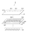
- FIG. 2 is an exploded perspective view of a print head.
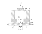
- FIG. 3 is a side sectional view of the print head.
- ink droplets upon landing when the surface of the substrate is 25 ° C.
- ink droplets upon landing at 100 ° C. a) ink droplets upon landing at 100 ° C.
- conductive layer at 25 ° C. a conductive layer at 100 ° C.
- d Enlarged photographs of the conductive layer at 100 ° C. It is a figure which shows the measurement result of the landing diameter in the present Example 2.
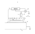
- FIG. 1 is a schematic diagram showing the overall configuration of the ink jet apparatus 1.
- the inkjet apparatus 1 includes a print head 2 on which nozzles 211 that discharge ink droplets R of ink I having charging properties are formed, and a facing surface that faces the nozzles 211 of the print head 2.
- a counter electrode 3 that supports the substrate 11 that receives the landing of the ink droplet R, a control unit 4 that drives the print head 2 to eject the ink droplet R from the nozzle 211, and a heating unit 5 that heats the substrate 11.
- the ink jet apparatus 1 is configured to land a conductive ink droplet R on a substrate 11 to form wiring on the surface of the substrate 11.
- the counter electrode 3 is a flat plate that supports the substrate 11 via the heating means 5, and is arranged parallel to the ink ejection surface 211 c of the print head 2 and separated by a predetermined distance.
- the separation distance between the counter electrode 3 and the print head 2 is appropriately set within a range of about 0.1 to 5.0 mm.
- the counter electrode 3 is grounded and is always maintained at the ground potential. Therefore, as will be described later, when the charged ink droplet R lands on the substrate 11, the counter electrode 3 releases the electric charge by grounding.
- a heat insulating material (not shown) for insulating heat from the heating means 5 is provided on the upper surface of the counter electrode 3. ing. Further, the counter electrode 3 can be moved parallel to the surface supporting the substrate 11.
- the control means 4 is a computer composed of a CPU, ROM, RAM, etc. (not shown), an electrostatic voltage power source 41 for applying an electrostatic voltage to the print head 2, a heating means 5, and a piezoelectric element 23 of the print head 2 described later. Connected with.
- the control means 4 controls the electrostatic voltage power source 41 to apply an electrostatic voltage to the print head 2, thereby generating an electrostatic field between the nozzle plate 21 of the print head 2 and the counter electrode 3.
- the heating means 5 is controlled to heat the substrate 11, and the deformation of the piezoelectric element 23 is controlled to eject the ink droplet R from the nozzle 211.
- the control unit 4 can control scanning of the print head 2.
- the voltage applied by the electrostatic voltage power supply 41 is a direct current, but may be an alternating current.
- the print head 2 may be grounded by connecting the electrostatic voltage power source 41 to the counter electrode 3 and applying a voltage to the counter electrode 3.
- the control means 4 may be configured to perform scanning control on the stage of the counter electrode 3 (the surface that supports the substrate 11) while the print head 2 is fixed.
- the heating means 5 is a thin plate-like polyimide heater and is laid on the upper surface of the counter electrode 3.
- the heating means 5 heats the substrate 11 placed on the upper surface by being controlled by the control means 4.
- the heating means 5 may not be a polyimide heater as long as the substrate 11 can be heated without shielding the electrostatic field generated between the print head 2 and the counter electrode 3, and is configured integrally with the counter electrode 3. You may let them. However, it is preferable that the surface of the substrate 11 (the landing surface of the ink droplet R) 11a can be heated uniformly.
- the substrate 11 is a silicon semiconductor chip or semiconductor wafer formed to a thickness of about several hundred ⁇ m.
- a plurality of electrodes (for example, pads) 112 an integrated circuit (not shown) (for example, a circuit having a transistor and a memory) and the like are mounted, and a conductive layer 12 for electrically connecting them is provided. It is drawn with a predetermined wiring pattern.
- the conductive layer 12 is formed by drying the ink droplets R of the ink I ejected from the print head 2 and sintering the metal nanoparticles contained in the ink I by a method described later.
- the substrate 11 has at least one insulating film (not shown) formed thereon.
- This insulating film is called a passivation film, and can be formed of, for example, SiO 2 , Si 3 N 4 , polyimide resin, or the like.
- the electrode 112 disposed on the surface 11a of the substrate 11 is made of an aluminum-based metal and is not particularly limited, but the shape of the surface 112a is rectangular.
- the electrode 112 is a terminal when the substrate 11 is connected to another substrate or an electronic component.
- the ink I ejected from the print head 2 is an ink having conductivity and chargeability by dispersing metal nanoparticles.
- the metal nanoparticles include silver, gold, copper, palladium, platinum, nickel, rhodium, tin, indium, and alloys thereof.
- the physical method is generally a method for producing nanoparticles by pulverizing bulk metal
- the chemical method is a method for producing nanoparticles by generating metal atoms and controlling their aggregation.
- the chemical reduction method which is well known as a wet method, is a method of generating nanoparticles by reducing metal ions by adding a reducing agent to a metal ion solution or heating a metal salt solution containing a reducing agent. is there.
- the ink in which such nanoparticles are dispersed for example, the ink disclosed in Japanese Patent No. 3933138 can be used.
- a gas evaporation method is known as a dry method.
- the gas evaporation method is a method in which a metal is evaporated in an inert gas and cooled and aggregated by collision with the gas to generate nanoparticles. It is known that the particle size of the dry method can be made smaller than that of the wet method, and nanoparticles having a particle size of about several nm can be generated by the dry method.
- the particle size of the metal nanoparticles in the ink I used in the present embodiment is 1 to 100 nm, preferably 1 to 50 nm. Although metal nanoparticles having a particle size of less than 1 nm may be used, such particles are extremely difficult to produce and are not practical. Further, when metal nanoparticles having a particle diameter exceeding 100 nm are used, the nozzle 211 may be clogged.
- the concentration of the metal nanoparticles dispersed in the ink I is preferably high so that the resistance value of the conductive layer 12 formed by drying the ink I becomes a value closer to the resistance value of the electrode 112. . Specifically, 10 mass% or more is preferable and 20 mass% or more is more preferable. However, the concentration of the metal nanoparticles can be about 80% by mass at maximum.
- water or a water-soluble organic solvent is used as a solvent for dispersing the metal nanoparticles.
- a so-called water-based ink is superior in electric conductivity as compared with an oil-based ink using a nonpolar solvent.
- this solvent preferably has a low vapor pressure and a high boiling point so that the viscosity of the ink I does not easily rise or dry.
- a boiling point of a solvent 150 degreeC or more is preferable and 200 degreeC or more is more preferable.
- the water content is preferably 40% by mass or less from the viewpoint of drying properties.
- the viscosity of the ink I is preferably 2 mPa ⁇ s or more and 10 mPa ⁇ s or less at the discharge temperature, more preferably 3 mPa ⁇ s or more and 6.5 mPa ⁇ s or less.
- the discharge temperature is preferably 20 to 60 ° C, more preferably 25 to 50 ° C. If the temperature is lower than 25 ° C., heating may be required. If the temperature exceeds 50 ° C., the print head 2 and the ink I flow path member may be burdened.
- the surface tension of the ink I is preferably 20 mN / m or more and 50 mN / m or less. Furthermore, from the viewpoint of ejection stability, it is more preferably 25 mN / m or more and 45 mN / m or less.
- the electrical conductivity of the ink I is preferably 0.1 ⁇ S / cm or more and 2000 ⁇ S / cm or less at 25 ° C. in order to apply an electrostatic attraction force.
- 1 ⁇ S / cm or more and 1000 ⁇ S / cm More preferable is cm or less.
- the relative dielectric constant of ink I is preferably 10 or more.
- FIG. 2 is an exploded perspective view of the print head 2
- FIG. 3 is a side sectional view of the print head 2.
- the print head 2 includes a nozzle plate 21, a body plate 22, and a piezoelectric element 23.
- the nozzle plate 21 is a silicon substrate or a silicon oxide substrate having a thickness of about 150 to 300 ⁇ m.
- a plurality of nozzles 211 are formed on the nozzle plate 21, and the plurality of nozzles 211 are arranged in a line.
- the body plate 22 is a silicon substrate having a thickness of about 200 to 500 ⁇ m.
- an ink supply port 221, an ink storage chamber 222, a plurality of ink supply paths 223, and a plurality of pressure chambers 224 are formed.
- the ink supply port 221 is a circular through hole having a diameter of about 400 to 1500 ⁇ m.
- the ink storage chamber 222 is a groove having a width of about 400 to 1000 ⁇ m and a depth of about 50 to 200 ⁇ m.
- the ink supply path 223 is a groove having a width of about 50 to 150 ⁇ m and a depth of about 30 to 150 ⁇ m.
- the pressure chamber 224 is a groove having a width of about 150 to 350 ⁇ m and a depth of about 50 to 200 ⁇ m.
- the nozzle plate 21 and the body plate 22 are joined to each other, and in the joined state, the nozzle 211 of the nozzle plate 21 and the pressure chamber 224 of the body plate 22 are in a one-to-one correspondence. .
- the ink When ink is supplied to the ink supply port 221 in a state where the nozzle plate 21 and the body plate 22 are joined, the ink is temporarily stored in the ink storage chamber 222, and then each ink supply from the ink storage chamber 222 is performed.
- the pressure chambers 224 are supplied through the passages 223.
- the piezoelectric element 23 is bonded to a position corresponding to the pressure chamber 224 of the body plate 22.
- the piezoelectric element 23 is an actuator made of PZT (lead Zirconium Titanate), and is deformed when a voltage is applied to eject ink inside the pressure chamber 224 from the nozzle 211.
- a borosilicate glass plate 24 (see FIG. 3) is interposed between the nozzle plate 21 and the body plate 22.
- one nozzle 211 and one pressure chamber 224 are formed corresponding to one piezoelectric element 23.
- a step is formed in the nozzle 211, and the nozzle 211 includes a lower step portion 211a and an upper step portion 211b.
- the lower step portion 211a and the upper step portion 211b both have a cylindrical shape, and the diameter S1 of the lower step portion 211a (the distance in the left-right direction in FIG. 3) is smaller than the diameter S2 of the upper step portion 211b (the distance in the left-right direction in FIG. 3). It has become.
- the lower part 211a of the nozzle 211 is a part that directly ejects ink circulated from the upper part 211b.
- the lower step portion 211a has a diameter S1 of 1 to 10 ⁇ m and a length H (distance in the vertical direction in FIG. 3) of 1.0 to 5.0 ⁇ m.
- the reason why the length H of the lower step portion 211a is limited to the range of 1.0 to 5.0 ⁇ m is that the ink landing accuracy can be remarkably improved.
- the upper part 211b of the nozzle 211 is a part for allowing the ink circulated from the pressure chamber 224 to circulate to the lower part 211a, and its diameter S2 is 10 to 60 ⁇ m.
- the lower limit of the diameter S2 of the upper step portion 211b is limited to 10 ⁇ m or more. If the lower limit is less than 10 ⁇ m, the flow passage resistance of the upper step portion 211b cannot be ignored with respect to the flow passage resistance of the entire nozzle 211 (lower step portion 211a and upper step portion 211b). This is because the ink ejection efficiency decreases.
- the upper limit of the diameter S2 of the upper step portion 211b is limited to 60 ⁇ m or less because the lower step portion 211a as the ink ejection site becomes thinner as the diameter S2 of the upper step portion 211b increases (the area of the lower step portion 211a increases). This is because the mechanical strength is reduced), and the ink is easily deformed when ejected, and as a result, the ink landing accuracy is lowered. That is, when the upper limit of the diameter S2 of the upper step portion 211b exceeds 60 ⁇ m, the deformation of the lower step portion 211a becomes very large as the ink is discharged, and the landing accuracy is a specified value ( ⁇ 0.5 ° with respect to a desired discharge direction). This is because there is a possibility that it will not be able to be suppressed within.
- a borosilicate glass plate 24 having a thickness of about several hundred ⁇ m is provided between the nozzle plate 21 and the body plate 22, and the borosilicate glass plate 24 has an opening for communicating the nozzle 211 and the pressure chamber 224.
- a portion 24a is formed.
- the opening 24 a is a through hole that communicates with the pressure chamber 224 and the upper stage portion 211 b of the nozzle 211, and is a part that functions as a flow path through which ink flows from the pressure chamber 224 toward the nozzle 211.
- the pressure chamber 224 is a portion that receives pressure from the piezoelectric element 23 and applies pressure to the ink inside the pressure chamber 224.
- the print head 2 is provided in the apparatus main body so that it can be scanned in a direction substantially parallel to the ink ejection surface 211c (X direction in FIG. 1) by a mechanism (not shown).
- a conductive layer forming step is performed.
- the ink droplet R is landed on the surface 11 a of the substrate 11 from the print head 2 to form the conductive layer 12.
- the substrate 11 is placed on the heating means 5 and positioned and fixed to the counter electrode 3.
- the distance between the ink ejection surface 211c of the print head 2 and the surface 11a of the substrate 11 is appropriately adjusted so as to be 3 mm or more and 5 mm or less. If this distance is less than 3 mm, the radiant heat from the substrate 11 heated by the heating means 5 raises the temperature of the print head 2, causing thermal deformation of the nozzle 211 and drying of the ink I in the nozzle 211. As a result, the discharge accuracy of the ink droplet R is lowered. On the other hand, if the distance exceeds 5 mm, it is necessary to increase the voltage applied to the print head 2 for properly flying the ink droplet R from the print head 2 to the substrate 11, resulting in an increase in the size of the apparatus.
- an electrostatic field is generated between the nozzle plate 21 and the counter electrode 3 by controlling the electrostatic voltage power supply 41 by the control means 4 and applying an electrostatic voltage to the print head 2. Due to the electrostatic field, electric lines of force from the print head 2 to the substrate 11 are formed. At this time, care is taken that the potential difference generated between the print head 2 and the substrate 11 is less than the dielectric breakdown voltage of air (about 3.55 kV / mm).
- the control means 4 controls the heating means 5 to heat the substrate 11 so that the surface 11a of the substrate 11 reaches a predetermined temperature.
- the predetermined temperature at this time is preferably a temperature equal to or higher than the lowest boiling temperature among the boiling points of the main solvent contained in the ink I, and is preferably equal to or lower than a firing temperature described later.
- the main solvent contained in the ink I refers to a solvent contained in the ink I by about 5% by mass or more.
- the temperature of the surface 11a of the substrate 11 is measured by a temperature sensor (not shown), and the heating unit 5 is controlled by the control unit 4 so that the measured temperature becomes the predetermined temperature.
- the ink droplet R is ejected from the nozzle 211 of the print head 2 toward the surface 11a of the substrate 11 while scanning the print head 2 substantially parallel to the surface 11a of the substrate 11.
- the ejection of the ink droplets R is continuously performed so that the ink droplets R that land on the surface 11a of the substrate 11 form a predetermined wiring pattern stored in advance in the control unit 4 while overlapping.
- the ink droplet R ejected from the print head 2 is adjusted to an ejection amount within an appropriate range.
- the appropriate discharge amount of the ink droplet R differs depending on the contact angle of the ink droplet R with the surface 11a of the substrate 11 as well as the distance between the print head 2 and the surface 11a of the substrate 11 and the heating temperature of the surface 11a. , And appropriately adjusted according to these conditions.
- the diameter of the ink droplet R upon landing depends on the physical properties of the ink I and the surface energy or surface state of the landing substrate 11, but when landing on the substrate 11 that does not absorb the ink I, the flying time is as follows. The diameter is about 1.5 to 4.0 times.
- the ink droplet R ejected from the print head 2 flies along an electric force line from the print head 2 to the substrate 11, that is, flies by receiving an electrostatic attraction force toward the substrate 11 due to an electrostatic field, and flies. Land on the surface 11a.
- the ink droplet R that has landed on the surface 11a of the substrate 11 is quickly dried without spreading due to the surface 11a being heated to the predetermined temperature.
- the flight distance of the ink droplet R can be increased as compared with the conventional on-demand type ink jet head, and the surface of the substrate 11
- the distance between the print head 2 and the substrate 11 can be increased as compared with the prior art, and the solidification of the landed ink droplets R can be accelerated while preventing radiant heat transfer from the substrate 11 to the print head 2.
- the ink droplet R is continuously landed across the surface 11 a of the substrate 11 and the surface 112 a of the electrode 112.
- the surface 11a of the substrate 11 and the surface 112a of the electrode 112 in addition to the difference in the contact angle inherent to the material, the surface 112a of the electrode 112 is a rougher surface. Shows high hydrophilicity.
- the ink droplets R that are continuously landed on the surface 11a of the substrate 11 and the surface 112a of the electrode 112 are more hydrophilic than the surface 112a of the electrode 112. Without being pulled toward the surface 11a of the substrate 11, it is quickly dried at the landed position.
- the conductive layer 12 having a predetermined wiring pattern is formed on the surface 11a of the substrate 11, and the conductive layer forming step is completed.
- the conductive layer 12 is fired.
- Calcination method includes drying in a dryer or hot plate.
- a subbing agent a silane coupling agent or a titanium coupling agent
- sintering under conditions that can ensure the heat resistance of various coupling agents is preferable.
- the solvent remains in the fused metal, and the resistance value may increase.
- the temperature of the preliminary drying is less than 100 ° C., the solvent hardly evaporates and there is a possibility that the effect does not occur, and when the temperature exceeds 150 ° C., the fusion of the metal nanoparticles may start. If the sintering temperature is less than 150 ° C., the metal nanoparticles are not fused, and the resistance value may be increased.
- the subbing agent deteriorates and mixes with the fusion metal, resulting in resistance.
- the value may be high.
- a hot plate is preferably used for the main sintering. This is because when the hot plate is used, heat is directly transmitted to the ink I, and the fusion of the metal nanoparticles is facilitated.
- preliminary drying may be omitted.
- the solvent of the ink droplet R is evaporated by the above baking, so that the conductive layer 12 is fixed to the substrate 11.
- the distance between the print head 2 and the substrate 11 is made larger than in the past, and radiation heat transfer from the substrate 11 to the print head 2 is prevented and landed.
- the high-definition conductive layer 12 can be formed in a short time while reliably preventing the ink droplet R from being discharged accurately.
- the ink droplets R continuously landed on the surface 11a of the substrate 11 and the surface 112a of the electrode 112 are not pulled toward the surface 11a of the substrate 11 having higher hydrophilicity than the surface 112a of the electrode 112. Since the ink is quickly dried at the landing position, it is possible to prevent the ink droplets R from collecting.
- the surface 11a is heated while measuring the temperature of the surface 11a of the substrate 11 by a temperature sensor (not shown).
- a step of setting heating conditions before the conductive layer forming step is performed. It is also possible to confirm the setting of the heating means 5 at which the surface 11a of the substrate 11 becomes a predetermined temperature in the process, and to configure the heating means 5 to be controlled by this setting in the conductive layer forming process.
- the electrode 112 is described as the substrate member having a surface having a hydrophilic property different from that of the surface 11a of the substrate 11.
- the substrate 112 is not limited to the electrode 112, and It may have a surface that is more hydrophilic than the surface 11a.
- Example 1 Hereinafter, the present invention will be described more specifically with reference to examples.
- the conductive layer 12 was formed on the surface 11a of the substrate 11 under the following conditions.
- ⁇ Board> As the substrate 11, a silicon semiconductor wafer having an insulating film formed on the surface thereof was used.
- ⁇ Used ink> Ag ink was used as ink I.
- the main components of this Ag ink are silver solid content: 15% by mass, DEGBE (diethylene glycol monobutyl ether): 71.315% by mass, water: 8.755% by mass, and 2-pyrrolidone: 4.93% by mass.
- DEGBE, water, and 2-pyrrolidone as solvents have boiling points of 245 ° C., 100 ° C., and 230 ° C., respectively.
- the contact angle of the ink I with respect to the surface 11a of the substrate 11 is about 10 °.
- the surface 11a of the substrate 11 is heated to 25 ° C., 40 ° C., 60 ° C., 80 ° C., 100 ° C., 130 ° C., 150 ° C., 180 ° C., and 200 ° C. by the heating means 5 and conductive at each temperature.
- Layer 12 was formed.
- the distance between the ink ejection surface 211c of the print head 2 and the surface 11a of the substrate 11 was changed to a value shown in Table 1 described later with respect to each of the above temperatures so that the temperature of the print head 2 did not increase.
- the electrostatic voltage applied to the print head 2 was adjusted in the range of 2 to 9 kV so that the potential difference between the ink ejection surface 211c of the print head 2 and the surface 11a of the substrate 11 was about 2 kV / mm.
- the ink droplet R was discharged while the print head 2 was scanned.
- the ejection amount (volume) of the ink droplet R was 0.5 pl.
- the scanning speed of the print head 2 was set to a speed at which the ink droplets R landed continuously on the surface 11a of the substrate 11 overlap each other by half the diameter.
- a drive voltage of 20 V was applied to the piezoelectric element 23 of the print head 2.
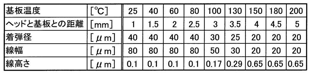
- Table 1 shows the landing diameter of the ink droplet R, the line width and the line height of the conductive layer 12 when the temperature of the surface 11a of the substrate 11 in the formation of the conductive layer is changed.
- FIG. 4A to FIG. 4D show enlarged photographs of the ink droplet R (one droplet) and the conductive layer 12 at the time of landing when the temperature of the surface 11a of the substrate 11 is 25 ° C. and 100 ° C. 4A to 4D are all magnified photographs at the same magnification.
- the temperature of the surface 11a of the substrate 11 exceeded 100 ° C.
- the same tendency as in the case of the discharge amount of 0.5 pl was obtained, in which the landing diameter was reduced and the line width of the conductive layer 12 was narrowed and the line height was increased.
- the numerical values such as the landing diameter of the ink droplet R were not different from those at 180 ° C., but irregularities were confirmed on the surface of the conductive layer 12. This is presumed to be because the solvent contained in the ink I has suddenly boiled, so it is considered that the heating temperature of the surface 11a of the substrate 11 is preferably 180 ° C. or less, which is the firing temperature of the ink I. (Example 2)
- the ink droplet R was landed on the surface 11a of the substrate 11 under the following conditions, and the landing diameter was measured.
- the conditions other than those described below are the same as in the first embodiment.
- ⁇ Board> As the substrate 11, a silicon semiconductor wafer having a surface 11a subjected to Ti-based subbing treatment was used. Moreover, the contact angle of the ink I with respect to the surface 11a was about 20 ° by this subtraction process.
- ⁇ Conductive layer formation> The surface 11a of the substrate 11 is heated to each temperature of 25 ° C. and 130 ° C. by the heating means 5, and the ejection amount (volume) of the ink droplet R is 0.5 to 5.5 pl with respect to the surface 11a of the substrate 11 at each temperature. The ink droplet R was landed while changing by 0.5 pl in the range of.
- ⁇ Results and summary> The measurement result of the landing diameter of the ink droplet R is shown in FIG.
- Inkjet device (wiring forming device) 2 Print head 3 Counter electrode (support member) 4 Control means 5 Heating means 11 Substrate 11a Surface 12 Conductive layer 41 Electrostatic voltage power supply (voltage application means) 112 Electrode (substrate member) 112a Surface (other surfaces) 211c Ink ejection surface I Ink R Ink droplet
Landscapes
- Engineering & Computer Science (AREA)
- Manufacturing & Machinery (AREA)
- Microelectronics & Electronic Packaging (AREA)
- Coating Apparatus (AREA)
- Electrodes Of Semiconductors (AREA)
- Internal Circuitry In Semiconductor Integrated Circuit Devices (AREA)
- Application Of Or Painting With Fluid Materials (AREA)
- Manufacturing Of Printed Wiring (AREA)
Abstract
インク滴の吐出精度の低下を確実に防止しつつ、高精細な導電層を短時間に形成することを目的とし、インクIとして帯電性を有するものを用い、プリントヘッド2と基板11との間に電圧を印加するとともに、インクIに含有される主たる溶媒の各沸点温度のうち最も低い沸点温度以上に基板11の表面11aを加熱した状態で、プリントヘッド2からインクIのインク滴Rを吐出させて、基板11の表面11aに導電層12を形成する。
Description
本発明は、配線形成方法及び配線形成装置に関する。
近年、半導体チップに配線パターンを描画する方法として、インクジェットヘッドから導電性のインク滴を吐出させて、配線状の導電層を形成する方法が注目されている(例えば、特許文献1~3参照)。
このインクジェット方式による配線形成方法においては、半導体チップ(基板)を加熱した状態で連続的にインク滴を着弾させることで、着弾したインク滴の濡れ広がりを防止して速やかに乾燥させ、高精細な導電層を短時間に形成できることが知られている。
ところが、単純に基板を加熱した場合、この基板とインクジェットヘッドとが近接しているために、インクジェットヘッドは加熱された基板から輻射熱を受け、基板同様に加熱されてしまう。その結果、インクジェットヘッドのノズルが熱変形を起こしたり、ノズル内のインクの粘度が下がるなどして、インク滴の吐出精度が低下するといった問題が生じる。
そこで、基板を加熱する加熱部の両端にインクジェットヘッドを冷却する冷却部を並設し、加熱部に載置された基板の上方でインク滴を吐出したのち冷却部の上方を通過するようインクジェットヘッドを走査させることにより、基板からの輻射熱で加熱されたインクジェットヘッドを冷却する方法が提案されている(例えば、特許文献4参照)。
しかしながら、上記特許文献4に記載の方法では、基板からインクジェットヘッドへの輻射伝熱を防ぐことができていないために、一時的にせよインクジェットヘッドの温度上昇は避けられない。そのため、この温度上昇分のノズルの熱変形やインクの乾燥が生じてしまい、結果として吐出精度の低下を確実に防止するには至っていなかった。
また、このような吐出精度の低下を防ぐ目的で、単純にインクジェットヘッドを基板から離間させて当該インクジェットヘッドの温度上昇の回避を試みても、一般的なオンデマンド型のインクジェットヘッドが使用されているためにインク滴の飛翔距離が短く、所定距離以上に離間させることができなかった。そのため、インクジェットヘッドが温度上昇しないよう基板の加熱温度に制限を設ける必要が生じ、結果として高精細な導電層を短時間に形成することができていなかった。
本発明は、上記事情を鑑みてなされたもので、インク滴の吐出精度の低下を確実に防止しつつ、高精細な導電層を短時間に形成できる配線形成方法及び配線形成装置の提供を課題とする。
前記の課題を解決するために、請求項1に記載の発明は、
インクジェット方式のプリントヘッドから、導電性材料を含有するインクのインク滴を吐出させて基板へ着弾させ、当該基板の表面に配線を形成する配線形成方法であって、
前記インクとして帯電性を有するものを用い、前記プリントヘッドと前記基板との間に電圧を印加するとともに、前記インクに含有される主たる溶媒の各沸点温度のうち最も低い沸点温度以上に前記基板の表面を加熱した状態で、前記プリントヘッドから前記インクのインク滴を吐出させて、前記基板の表面に前記配線としての導電層を形成することを特徴とする。
インクジェット方式のプリントヘッドから、導電性材料を含有するインクのインク滴を吐出させて基板へ着弾させ、当該基板の表面に配線を形成する配線形成方法であって、
前記インクとして帯電性を有するものを用い、前記プリントヘッドと前記基板との間に電圧を印加するとともに、前記インクに含有される主たる溶媒の各沸点温度のうち最も低い沸点温度以上に前記基板の表面を加熱した状態で、前記プリントヘッドから前記インクのインク滴を吐出させて、前記基板の表面に前記配線としての導電層を形成することを特徴とする。
請求項2に記載の発明は、請求項1に記載の配線形成方法であって、
前記プリントヘッドのインク吐出面と前記基板の表面との距離は、3mm以上5mm以下であることを特徴とする。
前記プリントヘッドのインク吐出面と前記基板の表面との距離は、3mm以上5mm以下であることを特徴とする。
請求項3に記載の発明は、請求項1又は2に記載の配線形成方法であって、
前記基板として、当該基板の表面とは親水性の異なる他の表面を有する基板部材が、当該他の表面を前記プリントヘッドのインク吐出面に露出させるよう、当該基板の表面に配設されたものを用い、
前記基板の表面と前記基板部材の他の表面とに跨って前記インクのインク滴が連続的に着弾するように、前記プリントヘッドから前記インクのインク滴を吐出させて、当該基板の表面と当該基板部材の他の表面とに前記配線としての導電層を形成することを特徴とする。
前記基板として、当該基板の表面とは親水性の異なる他の表面を有する基板部材が、当該他の表面を前記プリントヘッドのインク吐出面に露出させるよう、当該基板の表面に配設されたものを用い、
前記基板の表面と前記基板部材の他の表面とに跨って前記インクのインク滴が連続的に着弾するように、前記プリントヘッドから前記インクのインク滴を吐出させて、当該基板の表面と当該基板部材の他の表面とに前記配線としての導電層を形成することを特徴とする。
請求項4に記載の発明は、
基板の表面に配線を形成する配線形成装置であって、
帯電性を有するとともに導電性材料を含有するインクのインク滴を吐出するインクジェット方式のプリントヘッドと、
前記プリントヘッドのインク吐出面に前記基板の表面が露出するよう当該基板を支持する支持部材と、
前記プリントヘッドと前記支持部材との間に電圧を印加する電圧印加手段と、
前記基板の表面を加熱する加熱手段と、
を備え、
前記電圧印加手段により前記プリントヘッドと前記支持部材との間に電圧を印加するとともに、前記加熱手段により、前記インクに含有される主たる溶媒の各沸点温度のうち最も低い沸点温度以上に前記基板の表面を加熱した状態で、前記プリントヘッドから前記インクのインク滴を吐出させて前記基板へ着弾させ、前記基板の表面に前記配線としての導電層を形成することを特徴とする。
基板の表面に配線を形成する配線形成装置であって、
帯電性を有するとともに導電性材料を含有するインクのインク滴を吐出するインクジェット方式のプリントヘッドと、
前記プリントヘッドのインク吐出面に前記基板の表面が露出するよう当該基板を支持する支持部材と、
前記プリントヘッドと前記支持部材との間に電圧を印加する電圧印加手段と、
前記基板の表面を加熱する加熱手段と、
を備え、
前記電圧印加手段により前記プリントヘッドと前記支持部材との間に電圧を印加するとともに、前記加熱手段により、前記インクに含有される主たる溶媒の各沸点温度のうち最も低い沸点温度以上に前記基板の表面を加熱した状態で、前記プリントヘッドから前記インクのインク滴を吐出させて前記基板へ着弾させ、前記基板の表面に前記配線としての導電層を形成することを特徴とする。
請求項1に記載の発明によれば、プリントヘッドと基板との間に電圧を印加しつつ、インクに含有される主たる溶媒の各沸点温度のうち最も低い沸点温度以上に基板の表面を加熱した状態でインク滴を吐出させるので、吐出されたインク滴に対し基板へ向かう静電吸引力を作用させ、従来のオンデマンド型のインクジェットヘッド(プリントヘッド)に比べインク滴の飛翔距離を伸ばすとともに、着弾したインク滴の濡れ広がりを防止して速やかに乾燥させる。これにより、従来よりもプリントヘッドと基板との距離を離間させ、基板からプリントヘッドへの輻射伝熱を防ぎつつ、着弾させたインク滴の固化を早めることができる。したがって、インク滴の吐出精度の低下を確実に防止しつつ、高精細な導電層を短時間に形成することができる。
請求項3に記載の発明によれば、基板として、この基板の表面とは親水性の異なる他の表面を有する基板部材が表面に配設されたものを用い、この基板の表面と基板部材の他の表面とに跨ってインク滴を連続的に着弾させる。このとき、基板の表面が加熱されているため、インク滴は、基板の表面と基板部材の他の表面とのうち親水性の高い方に引っ張られることなく、着弾した位置で速やかに乾燥される。したがって、親水性の異なる部材間にインク滴を着弾させた場合であっても、当該インク滴の液溜まりを防止することができる。
以下、本発明の実施の形態について、図を参照して説明する。
まず、本実施の形態に係るインクジェット装置1の全体構成について、図1を参照して説明する。
図1は、インクジェット装置1の全体構成を示す模式図である。
図1に示すように、インクジェット装置1は、帯電性を有するインクIのインク滴Rを吐出するノズル211が形成されたプリントヘッド2と、プリントヘッド2のノズル211に対向する対向面を有するとともに、インク滴Rの着弾を受ける基板11を支持する対向電極3と、プリントヘッド2を駆動させてノズル211からインク滴Rを吐出させる制御手段4と、基板11を加熱する加熱手段5とを備えている。このインクジェット装置1は、導電性を有するインク滴Rを基板11に着弾させて、当該基板11の表面に配線を形成するものである。
対向電極3は、加熱手段5を介して基板11を支持する平板状のものであり、プリントヘッド2のインク吐出面211cに平行に所定距離だけ離間されて配置されている。対向電極3とプリントヘッド2との離間距離は、0.1~5.0mm程度の範囲内で適宜設定される。また、対向電極3は接地されており、常時接地電位に維持されている。そのため、後述するように、帯電したインク滴Rが基板11に着弾すると、対向電極3はその電荷を接地により逃がすようになっている。なお、対向電極3の上面には、基板11を位置決めして固定するための図示しない位置決め手段及び真空チャッキング手段のほか、加熱手段5からの熱を断熱するための図示しない断熱材が設けられている。また、対向電極3は、基板11を支持する面に平行な移動が可能になっている。
制御手段4は、図示しないCPUやROM、RAM等から構成されたコンピュータであり、プリントヘッド2に静電電圧を印加する静電電圧電源41、加熱手段5及び後述するプリントヘッド2の圧電素子23と接続されている。この制御手段4は、静電電圧電源41を制御してプリントヘッド2に静電電圧を印加することにより、プリントヘッド2のノズルプレート21と対向電極3との間に静電界を生じさせるほか、加熱手段5を制御して基板11を加熱させたり、圧電素子23の変形を制御してノズル211からインク滴Rを吐出させたりするように構成されている。また、制御手段4は、プリントヘッド2の走査を制御可能になっている。なお、静電電圧電源41が印加する電圧は直流であるが、交流であってもよい。また、静電電圧電源41を対向電極3に接続して当該対向電極3に電圧を印加し、プリントヘッド2を接地してもよい。また、制御手段4は、プリントヘッド2を固定した状態で、対向電極3のステージ(基板11を支持する面)を走査制御するように構成してもよい。
加熱手段5は、薄板状のポリイミドヒーターであり、対向電極3の上面に敷設されている。この加熱手段5は、制御手段4に制御されることにより、上面に載置される基板11を加熱する。なお、加熱手段5は、プリントヘッド2と対向電極3との間に生じる静電界をシールドすることなく基板11を加熱可能であれば、ポリイミドヒーターでなくともよいし、対向電極3と一体に構成させてもよい。但し、基板11の表面(インク滴Rの被着弾面)11aを均一に加熱できる構成が好ましい。
基板11は、数百μm程度の厚みに形成されたシリコン製の半導体チップ又は半導体ウエハである。基板11の表面11aには、電極(例えばパッド)112や、図示しない集積回路(例えばトランジスタやメモリを有する回路)等が複数実装されており、これらを電気的に接続するための導電層12が所定の配線パターンで描画されている。この導電層12は、後述する方法により、プリントヘッド2から吐出されたインクIのインク滴Rを乾燥させ、さらにインクI中に含有される金属ナノ粒子を焼結させて形成される。
また、基板11には、少なくとも1層の絶縁膜(図示せず)が形成されている。この絶縁膜は、パッシベーション膜と呼ばれ、例えば、SiO2、Si3N4、ポリイミド樹脂などで形成することができる。
基板11の表面11aに配設される電極112は、アルミニウム系の金属で形成されており、特に限定はされないが、その表面112aの形状が矩形となっている。この電極112は、基板11を別の基板又は電子部品と接続する際の端子である。
プリントヘッド2から吐出されるインクIは、金属ナノ粒子が分散されることにより導電性及び帯電性を有するインクである。この金属ナノ粒子としては、例えば、銀、金、銅、パラジウム、白金、ニッケル、ロジウム、錫、インジウム、又はこれらの合金が挙げられる。
このような金属ナノ粒子の製造方法としては、大きく二つに分類される。一つは物理法で、もう一つは化学法である。物理法は、一般にバルク金属を粉砕してナノ粒子を製造する方法であり、化学法は、金属原子を発生させてその凝集を制御してナノ粒子を製造する方法である。
化学法は、液中で行われる湿式法と、空気中もしくは減圧雰囲気中で行われる乾式法に大別される。湿式法としてよく知られている化学還元法は、金属イオン溶液に還元剤を添加するか、或いは還元剤を含む金属塩溶液を加熱することで金属イオンを還元し、ナノ粒子を生成する手法である。このようなナノ粒子が分散されたインクとしては、例えば、特許第3933138号公報に開示のものを用いることができる。乾式法としては、ガス中蒸発法が知られている。ガス中蒸発法は、不活性ガス中で金属を蒸発させ、ガスとの衝突により冷却凝集させてナノ粒子を生成する方法である。乾式法の方が湿式法よりも粒径を小さくできることが知られており、乾式法では数nm程度の粒径のナノ粒子も生成可能である。
本実施の形態で用いるインクI中の金属ナノ粒子の粒径は、1~100nmであり、好ましくは1~50nmである。粒径が1nm未満の金属ナノ粒子を用いてもよいが、このような粒子は製造が極めて困難であり、実用的でない。また、粒径が100nmを超える金属ナノ粒子を用いると、ノズル211に詰まる恐れがある。
インクI中に分散している金属ナノ粒子の濃度は、インクIを乾燥させて形成される導電層12の抵抗値が電極112の抵抗値により近い値となるよう、高濃度であることが好ましい。具体的には、10質量%以上が好ましく、20質量%以上がより好ましい。但し、この金属ナノ粒子の濃度は、最大で80質量%程度にすることが可能である。
インクIのうち金属ナノ粒子を分散させる溶媒としては、水や水溶性有機溶媒が用いられる。このような、いわゆる水系インクは、無極性溶媒を用いた油系インクに比べ、電気伝導度に優れている。また、この溶媒は、インクIの粘度が容易に上昇したり、乾燥したりしないために、蒸気圧が低く、沸点が高いことが好ましい。溶媒の沸点としては、150℃以上が好ましく、200℃以上がより好ましい。含水率は、乾燥性の点から40質量%以下が好ましい。
インクIの粘度は、吐出温度において、2mPa・s以上、10mPa・s以下が吐出安定性の観点から好ましく、3mPa・s以上、6.5mPa・s以下がより好ましい。吐出温度については、20~60℃が好ましく、25~50℃がより好ましい。25℃未満であると加熱の必要が生じる場合があり、50℃を超えるとプリントヘッド2及びインクIの流路部材等に負担がかかる恐れがあるためである。
インクIの表面張力は、20mN/m以上、50mN/m以下が好ましい。更には、吐出安定性の観点から、25mN/m以上、45mN/m以下がより好ましい。
インクIの電気伝導度は、静電吸引力を作用させるために、25℃において0.1μS/cm以上、2000μS/cm以下が好ましいが、高精細描画の観点から、1μS/cm以上、1000μS/cm以下がより好ましい。
インクIの比誘電率は、10以上であることが好ましい。
続いて、プリントヘッド2の構成の詳細について、図2,3を参照して説明する。
図2は、プリントヘッド2の分解斜視図であり、図3は、プリントヘッド2の側断面図である。
図2に示すように、プリントヘッド2は、ノズルプレート21、ボディプレート22及び圧電素子23を有している。ノズルプレート21は150~300μm程度の厚みを有したシリコン基板又は酸化シリコン基板である。ノズルプレート21には複数のノズル211が形成されており、これら複数のノズル211が1列に配列されている。
ボディプレート22は200~500μm程度の厚みを有したシリコン基板である。ボディプレート22にはインク供給口221、インク貯留室222、複数のインク供給路223及び複数の圧力室224が形成されている。インク供給口221は直径が400~1500μm程度の円形状の貫通孔である。インク貯留室222は幅が400~1000μm程度で深さが50~200μm程度の溝である。インク供給路223は幅が50~150μm程度で深さが30~150μm程度の溝である。圧力室224は幅が150~350μm程度で深さが50~200μm程度の溝である。
ノズルプレート21とボディプレート22とは互いに接合されるようになっており、接合した状態ではノズルプレート21のノズル211とボディプレート22の圧力室224とが1対1で対応するようになっている。
ノズルプレート21とボディプレート22とが接合された状態でインク供給口221にインクが供給されると、当該インクはインク貯留室222に一時的に貯留され、その後にインク貯留室222から各インク供給路223を通じて各圧力室224に供給されるようになっている。
圧電素子23はボディプレート22の圧力室224に対応した位置に接着されるようになっている。圧電素子23はPZT(lead zirconium titanate)からなるアクチュエータであり、電圧の印加を受けると変形して圧力室224の内部のインクをノズル211から吐出させるようになっている。
なお、図2では図示しないが、ノズルプレート21とボディプレート22と間には硼珪酸ガラスプレート24(図3参照)が介在している。
図3に示す通り、1つの圧電素子23に対応してノズル211と圧力室224とが1つずつ構成されている。
ノズルプレート21においてノズル211には段が形成されており、ノズル211は下段部211aと上段部211bとで構成されている。下段部211aと上段部211bとは共に円筒形状を呈しており、下段部211aの直径S1(図3中左右方向の距離)が上段部211bの直径S2(図3中左右方向の距離)より小さくなっている。
ノズル211の下段部211aは上段部211bから流通してきたインクを直接的に吐出する部位である。下段部211aは直径S1が1~10μmで、長さH(図3中上下方向の距離)が1.0~5.0μmとなっている。下段部211aの長さHを1.0~5.0μmの範囲に限定するのは、インクの着弾精度を飛躍的に向上させることができるからである。
他方、ノズル211の上段部211bは圧力室224から流通してきたインクを下段部211aに流通させる部位であり、その直径S2が10~60μmとなっている。上段部211bの直径S2の下限を10μm以上に限定するのは、10μmを下回ると、ノズル211全体(下段部211aと上段部211b)の流路抵抗に対し上段部211bの流路抵抗が無視できない値となり、インクの吐出効率が低下するからである。
逆に、上段部211bの直径S2の上限を60μm以下に限定するのは、上段部211bの直径S2が大きくなるほど、インクの吐出部位としての下段部211aが薄弱化して(下段部211aが面積増大して機械的強度が小さくなる。)、インクの吐出時に変形し易くなり、その結果インクの着弾精度が低下するからである。すなわち、上段部211bの直径S2の上限が60μmを上回ると、インクの吐出に伴い下段部211aの変形が非常に大きくなり、着弾精度を規定値(所望の吐出方向に対して±0.5°)以内に抑えることができなくなる可能性があるからである。
ノズルプレート21とボディプレート22との間には数百μm程度の厚みを有した硼珪酸ガラスプレート24が設けられており、硼珪酸ガラスプレート24にはノズル211と圧力室224とを連通させる開口部24aが形成されている。開口部24aは、圧力室224とノズル211の上段部211bとに通じる貫通孔であり、圧力室224からノズル211に向けてインクを流通させる流路として機能する部位である。圧力室224は、圧電素子23の変形を受けて当該圧力室224の内部のインクに圧力を与える部位である。
以上の構成を具備するプリントヘッド2では、圧電素子23が変形すると、圧力室224の内部のインクに圧力を与え、当該インクは圧力室224から硼珪酸ガラスプレート24の開口部24aを流通してノズル211に至り、最終的にノズル211の下段部211aから吐出されるようになっている。
また、プリントヘッド2は、図示しない機構により、インク吐出面211cに略平行な方向(図1のX方向)へ走査可能なよう装置本体に設けられている。
続いて、基板11の表面11aに導電層12を形成する配線形成方法について、図1を参照して説明する。
まず、導電層形成工程を行う。
この工程では、プリントヘッド2から基板11の表面11aにインク滴Rを着弾させて導電層12を形成する。
最初に、基板11を加熱手段5上に載置し、対向電極3に位置決めして固定する。ここでは、プリントヘッド2のインク吐出面211cと基板11の表面11aとの距離が、3mm以上5mm以下となるよう適宜調整する。この距離が3mm未満であると、加熱手段5に加熱される基板11からの輻射熱がプリントヘッド2の温度を上昇させてしまい、ノズル211の熱変形やノズル211内のインクIの乾燥が生じて、インク滴Rの吐出精度の低下を招いてしまう。また、当該距離が5mmを超えると、インク滴Rをプリントヘッド2から基板11へ適正に飛翔させるためのプリントヘッド2への印加電圧を大きくする必要が生じ、装置の大型化を招いてしまう。
次に、制御手段4により静電電圧電源41を制御してプリントヘッド2に静電電圧を印加することで、ノズルプレート21と対向電極3との間に静電界を生じさせる。この静電界により、プリントヘッド2から基板11へ向かう電気力線が形成される。このとき、プリントヘッド2と基板11との間に生じる電位差が、空気の絶縁破壊電圧(約3.55kV/mm)未満となるよう注意する。
これに併せて、制御手段4により加熱手段5を制御して、基板11の表面11aが所定温度となるよう当該基板11を加熱する。このときの所定温度は、インクIに含有される主たる溶媒の各沸点温度のうち最も低い沸点温度以上の温度とし、後述する焼成温度以下の温度とするのが好ましい。ここで、インクIに含有される主たる溶媒とは、インクIに約5質量%以上含有される溶媒を指す。なお、本実施の形態においては、図示しない温度センサにより基板11の表面11aの温度を計測しつつ、この計測温度が上記の所定温度となるよう制御手段4により加熱手段5を制御している。
この状態で、プリントヘッド2を基板11の表面11aと略平行に走査させながら、当該プリントヘッド2のノズル211から基板11の表面11aへ向けてインク滴Rを吐出させる。このインク滴Rの吐出は、基板11の表面11aに着弾する当該インク滴Rが、それぞれ重なりつつ制御手段4に予め記憶された所定の配線パターンを形成するよう連続的に行われる。
このとき、プリントヘッド2から吐出されるインク滴Rは、適切な範囲の吐出量に調整される。但し、このインク滴Rの適切な吐出量は、プリントヘッド2と基板11の表面11aとの距離や当該表面11aの加熱温度のほか、基板11の表面11aに対するインク滴Rの接触角によっても異なり、これらの条件に応じて適宜調整される。なお、インク滴Rの着弾時の直径は、インクIの物性や、着弾する基板11の表面エネルギー或いは表面状態等にもよるが、インクIを吸収しない基板11に着弾した場合には、飛翔時の直径の約1.5~4.0倍となる。
プリントヘッド2から吐出されたインク滴Rは、プリントヘッド2から基板11へ向かう電気力線に沿って飛翔する、つまり静電界により基板11へ向かう静電吸引力を受けて飛翔し、基板11の表面11aに着弾する。基板11の表面11aに着弾したインク滴Rは、当該表面11aが上記の所定温度まで加熱されていることにより、濡れ広がることなく速やかに乾燥される。
このように、インク滴Rに対し基板11へ向かう静電吸引力を作用させることにより、従来のオンデマンド型のインクジェットヘッドに比べインク滴Rの飛翔距離を伸ばすことができるとともに、基板11の表面11aを上記の所定温度まで加熱することにより、当該表面11aに着弾したインク滴Rの濡れ広がりを防止して速やかに乾燥させることができる。これにより、従来よりもプリントヘッド2と基板11との距離を離間させ、基板11からプリントヘッド2への輻射伝熱を防ぎつつ、着弾させたインク滴Rの固化を早めることができる。
また、電極112を電気的に接続するように導電層12が形成される場合には、基板11の表面11aと電極112の表面112aとに跨ってインク滴Rが連続的に着弾される。ここで、基板11の表面11aと電極112の表面112aとでは、材料固有の接触角の違いに加え、電極112の表面112aの方が粗い面であることも相まって、基板11の表面11aの方が高い親水性を示す。このとき、基板11の表面11aが加熱されているため、基板11の表面11aと電極112の表面112aとに連続的に着弾されたインク滴Rは、電極112の表面112aよりも親水性の高い基板11の表面11aの方に引っ張られることなく、着弾した位置で速やかに乾燥される。
こうして、基板11の表面11aに所定の配線パターンの導電層12が形成され、導電層形成工程が完了する。
次に、導電層12の焼成を行う。
焼成方法としては、乾燥機やホットプレートでの焼結などが挙げられる。本実施の形態では、インクIの濡れ性を制御し、着弾性を向上させるために、基板11の表面11aに下引き剤(シランカップリング剤やチタンカップリング剤)の塗布を行っている。そのため、各種カップリング剤の耐熱性が確保できる条件での焼結が好ましい。
この焼結は、100~150℃で10~30分の予備乾燥後、150~200℃で60~180分の本焼結を行うことが好ましい。予備乾燥を行わないと、融着した金属内に溶媒が残留し、抵抗値が上昇する恐れがある。予備乾燥の温度が100℃未満では溶媒の蒸発がほとんど起こらず、効果が生じない恐れがあり、150℃を超える温度では金属ナノ粒子の融着が始まる恐れがある。本焼結の温度が150℃未満では金属ナノ粒子の融着が起こらず、抵抗値が高くなる恐れがあり、200℃を超える温度では下引き剤が劣化して融着金属と混合し、抵抗値が高くなる恐れがある。本焼結にはホットプレートを用いるのが好ましい。ホットプレートを用いると、インクIに直接熱が伝わり、金属ナノ粒子の融着が進みやすくなるためである。
なお、導電層形成工程において基板11の表面11aを本焼結の温度近傍まで加熱した場合には、予備乾燥を省いてもよい。
上記の焼成でインク滴Rの溶媒が蒸発されることにより、導電層12が基板11に固定される。
以上のように、本実施の形態における配線形成方法によれば、従来よりもプリントヘッド2と基板11との距離を離間させ、基板11からプリントヘッド2への輻射伝熱を防ぐとともに、着弾させたインク滴Rの固化を早めることができるので、インク滴Rの吐出精度の低下を確実に防止しつつ、高精細な導電層12を短時間に形成することができる。
また、基板11の表面11aと電極112の表面112aとに連続的に着弾されたインク滴Rは、電極112の表面112aよりも親水性の高い基板11の表面11aの方に引っ張られることなく、着弾した位置で速やかに乾燥されるので、インク滴Rの液溜まりを防止することができる。
なお、本実施の形態においては、図示しない温度センサにより基板11の表面11aの温度を計測しつつ当該表面11aを加熱することとしたが、導電層形成工程の前に加熱条件を設定する工程を設けて、当該工程で基板11の表面11aが所定温度となる加熱手段5の設定を確認しておき、導電層形成工程では加熱手段5がこの設定で制御されるように構成してもよい。
また、本実施の形態においては、基板11の表面11aと親水性の異なる表面を有する基板部材として電極112を挙げて説明したが、当該電極112に限定されるものではなく、また、基板11の表面11aよりも親水性の高い表面を有するものであってもよい。
また、上記以外の点についても、本発明は上記実施の形態に限定されるものではなく、適宜変更可能であるのは勿論である。
(実施例1)
以下に、実施例を挙げることにより、本発明をさらに具体的に説明する。
(実施例1)
以下に、実施例を挙げることにより、本発明をさらに具体的に説明する。
本発明の実施例1として、以下の条件により、基板11の表面11aに導電層12を形成した。
<基板>
基板11として、表面に絶縁膜が形成されたシリコン製の半導体ウエハを使用した。
<使用インク>
インクIとしてAgインクを使用した。このAgインクの主要成分は、銀固型分:15質量%、DEGBE(ジエチレングリコールモノブチルエーテル):71.315質量%、水:8.755質量%、2-ピロリドン:4.93質量%である。このうち溶媒であるDEGBE、水、及び2-ピロリドンの沸点は、それぞれ245℃、100℃、及び230℃である。また、インクIの基板11の表面11aに対する接触角は約10°である。
<導電層形成>
基板11の表面11aを、加熱手段5により25℃、40℃、60℃、80℃、100℃、130℃、150℃、180℃、200℃の各温度に加熱して、当該各温度で導電層12を形成した。このとき、プリントヘッド2のインク吐出面211cと基板11の表面11aとの距離は、プリントヘッド2が温度上昇しないよう、上記の各温度に対し、後述する表1に示す値に変化させた。また、プリントヘッド2に印加する静電電圧は、プリントヘッド2のインク吐出面211cと基板11の表面11aとの電位差が約2kV/mmとなるよう、2~9kVの範囲で調整した。
<基板>
基板11として、表面に絶縁膜が形成されたシリコン製の半導体ウエハを使用した。
<使用インク>
インクIとしてAgインクを使用した。このAgインクの主要成分は、銀固型分:15質量%、DEGBE(ジエチレングリコールモノブチルエーテル):71.315質量%、水:8.755質量%、2-ピロリドン:4.93質量%である。このうち溶媒であるDEGBE、水、及び2-ピロリドンの沸点は、それぞれ245℃、100℃、及び230℃である。また、インクIの基板11の表面11aに対する接触角は約10°である。
<導電層形成>
基板11の表面11aを、加熱手段5により25℃、40℃、60℃、80℃、100℃、130℃、150℃、180℃、200℃の各温度に加熱して、当該各温度で導電層12を形成した。このとき、プリントヘッド2のインク吐出面211cと基板11の表面11aとの距離は、プリントヘッド2が温度上昇しないよう、上記の各温度に対し、後述する表1に示す値に変化させた。また、プリントヘッド2に印加する静電電圧は、プリントヘッド2のインク吐出面211cと基板11の表面11aとの電位差が約2kV/mmとなるよう、2~9kVの範囲で調整した。
この状態でプリントヘッド2を走査させつつ、インク滴Rの吐出を行った。インク滴Rの吐出量(体積)は0.5plとした。プリントヘッド2の走査速度は、基板11の表面11aに連続して着弾したインク滴Rが直径の半分だけ重なる速度とした。また、プリントヘッド2の圧電素子23には20Vの駆動電圧を印加した。
その後、着弾させたインク滴R(導電層12)を、180℃で100分間焼成した。
<結果>
導電層形成における基板11の表面11aの温度を変えたときのインク滴Rの着弾径、導電層12の線幅及び線高さを表1に示す。また、基板11の表面11aの温度を25℃,100℃にしたときの着弾時のインク滴R(1滴)、導電層12の拡大写真を図4(a)~(d)に示す。なお、図4(a)~(d)は全て同倍率での拡大写真である。また、上記の条件において、インク滴Rの吐出量を0.5plから変えた場合についても同様に計測を行ったが、基板11の表面11aの温度が100℃を超えたあたりからインク滴Rの着弾径が小さくなるとともに導電層12の線幅が細く線高さが高くなるといった、吐出量0.5plのときと同様の傾向が得られた。
<結果>
導電層形成における基板11の表面11aの温度を変えたときのインク滴Rの着弾径、導電層12の線幅及び線高さを表1に示す。また、基板11の表面11aの温度を25℃,100℃にしたときの着弾時のインク滴R(1滴)、導電層12の拡大写真を図4(a)~(d)に示す。なお、図4(a)~(d)は全て同倍率での拡大写真である。また、上記の条件において、インク滴Rの吐出量を0.5plから変えた場合についても同様に計測を行ったが、基板11の表面11aの温度が100℃を超えたあたりからインク滴Rの着弾径が小さくなるとともに導電層12の線幅が細く線高さが高くなるといった、吐出量0.5plのときと同様の傾向が得られた。
<まとめ>
表1に示す結果から、基板11の表面11aを100℃以上、つまりインクIに含まれる主たる溶媒のうち最も沸点温度の低い水の沸点温度以上とすることで、より高精細の導電層12を形成できていることが分かる。また、基板11の表面11aの温度を100~200℃の範囲に加熱した場合でも、プリントヘッド2と基板11との距離を3~5mmの範囲で適宜離間させることで、吐出精度を低下させることなく高精細な導電層12を形成できていることが分かる。
表1に示す結果から、基板11の表面11aを100℃以上、つまりインクIに含まれる主たる溶媒のうち最も沸点温度の低い水の沸点温度以上とすることで、より高精細の導電層12を形成できていることが分かる。また、基板11の表面11aの温度を100~200℃の範囲に加熱した場合でも、プリントヘッド2と基板11との距離を3~5mmの範囲で適宜離間させることで、吐出精度を低下させることなく高精細な導電層12を形成できていることが分かる。
また、図4(a)と図4(b)とを比較すると、基板11の表面11aを100℃にすることで、当該表面11aが常温(25℃)のときよりもインク滴Rの濡れ広がりを防止できていることが分かり、図4(c)と図4(d)とを比較すると、基板11の表面11aを100℃にすることで、当該表面11aが常温(25℃)のときよりも波打ちが少なく高精細な導電層12が形成できていることが分かる。
なお、基板11の表面11aを200℃にしたときには、インク滴Rの着弾径等の各数値は180℃のときと変わらないものの、導電層12の表面に凹凸が確認された。これはインクIに含有される溶媒が急激に沸騰したためと推測されることから、基板11の表面11aの加熱温度はインクIの焼成温度である180℃以下とするのが好ましいと考えられる。
(実施例2)
本発明の実施例2として、以下の条件で基板11の表面11aにインク滴Rを着弾させ、その着弾径を計測した。なお、以下に記載したもの以外の条件は、上記実施例1と同様である。
<基板>
基板11として、表面11aにTi系の下引き処理を施したシリコン製の半導体ウエハを使用した。また、この下引き処理により、当該表面11aに対するインクIの接触角は約20°となった。
<導電層形成>
基板11の表面11aを加熱手段5により25℃、130℃の各温度に加熱し、当該各温度の基板11の表面11aに対しインク滴Rの吐出量(体積)を0.5~5.5plの範囲で0.5plずつ変化させながら当該インク滴Rを着弾させた。
<結果及びまとめ>
インク滴Rの着弾径の計測結果を図5に示す。この図から、インク滴Rの吐出量が多いほど、基板11の表面11aが25℃のときと130℃のときとで着弾径の差が大きくなっていることが分かる。つまり、インク滴Rの吐出量が多いほど基板11の加熱による濡れ広がり防止の効果が大きいことが分かる。
(実施例2)
本発明の実施例2として、以下の条件で基板11の表面11aにインク滴Rを着弾させ、その着弾径を計測した。なお、以下に記載したもの以外の条件は、上記実施例1と同様である。
<基板>
基板11として、表面11aにTi系の下引き処理を施したシリコン製の半導体ウエハを使用した。また、この下引き処理により、当該表面11aに対するインクIの接触角は約20°となった。
<導電層形成>
基板11の表面11aを加熱手段5により25℃、130℃の各温度に加熱し、当該各温度の基板11の表面11aに対しインク滴Rの吐出量(体積)を0.5~5.5plの範囲で0.5plずつ変化させながら当該インク滴Rを着弾させた。
<結果及びまとめ>
インク滴Rの着弾径の計測結果を図5に示す。この図から、インク滴Rの吐出量が多いほど、基板11の表面11aが25℃のときと130℃のときとで着弾径の差が大きくなっていることが分かる。つまり、インク滴Rの吐出量が多いほど基板11の加熱による濡れ広がり防止の効果が大きいことが分かる。
1 インクジェット装置(配線形成装置)
2 プリントヘッド
3 対向電極(支持部材)
4 制御手段
5 加熱手段
11 基板
11a 表面
12 導電層
41 静電電圧電源(電圧印加手段)
112 電極(基板部材)
112a 表面(他の表面)
211c インク吐出面
I インク
R インク滴
2 プリントヘッド
3 対向電極(支持部材)
4 制御手段
5 加熱手段
11 基板
11a 表面
12 導電層
41 静電電圧電源(電圧印加手段)
112 電極(基板部材)
112a 表面(他の表面)
211c インク吐出面
I インク
R インク滴
Claims (4)
- インクジェット方式のプリントヘッドから、導電性材料を含有するインクのインク滴を吐出させて基板へ着弾させ、当該基板の表面に配線を形成する配線形成方法であって、
前記インクとして帯電性を有するものを用い、前記プリントヘッドと前記基板との間に電圧を印加するとともに、前記インクに含有される主たる溶媒の各沸点温度のうち最も低い沸点温度以上に前記基板の表面を加熱した状態で、前記プリントヘッドから前記インクのインク滴を吐出させて、前記基板の表面に前記配線としての導電層を形成することを特徴とする配線形成方法。 - 前記プリントヘッドのインク吐出面と前記基板の表面との距離は、3mm以上5mm以下であることを特徴とする請求項1に記載の配線形成方法。
- 前記基板として、当該基板の表面とは親水性の異なる他の表面を有する基板部材が、当該他の表面を前記プリントヘッドのインク吐出面に露出させるよう、当該基板の表面に配設されたものを用い、
前記基板の表面と前記基板部材の他の表面とに跨って前記インクのインク滴が連続的に着弾するように、前記プリントヘッドから前記インクのインク滴を吐出させて、当該基板の表面と当該基板部材の他の表面とに前記配線としての導電層を形成することを特徴とする請求項1又は2に記載の配線形成方法。 - 基板の表面に配線を形成する配線形成装置であって、
帯電性を有するとともに導電性材料を含有するインクのインク滴を吐出するインクジェット方式のプリントヘッドと、
前記プリントヘッドのインク吐出面に前記基板の表面が露出するよう当該基板を支持する支持部材と、
前記プリントヘッドと前記支持部材との間に電圧を印加する電圧印加手段と、
前記基板の表面を加熱する加熱手段と、
を備え、
前記電圧印加手段により前記プリントヘッドと前記支持部材との間に電圧を印加するとともに、前記加熱手段により、前記インクに含有される主たる溶媒の各沸点温度のうち最も低い沸点温度以上に前記基板の表面を加熱した状態で、前記プリントヘッドから前記インクのインク滴を吐出させて前記基板へ着弾させ、前記基板の表面に前記配線としての導電層を形成することを特徴とする配線形成装置。
Priority Applications (1)
| Application Number | Priority Date | Filing Date | Title |
|---|---|---|---|
| JP2010530805A JPWO2010035622A1 (ja) | 2008-09-26 | 2009-09-04 | 配線形成方法及び配線形成装置 |
Applications Claiming Priority (2)
| Application Number | Priority Date | Filing Date | Title |
|---|---|---|---|
| JP2008248999 | 2008-09-26 | ||
| JP2008-248999 | 2008-09-26 |
Publications (1)
| Publication Number | Publication Date |
|---|---|
| WO2010035622A1 true WO2010035622A1 (ja) | 2010-04-01 |
Family
ID=42059628
Family Applications (1)
| Application Number | Title | Priority Date | Filing Date |
|---|---|---|---|
| PCT/JP2009/065486 Ceased WO2010035622A1 (ja) | 2008-09-26 | 2009-09-04 | 配線形成方法及び配線形成装置 |
Country Status (2)
| Country | Link |
|---|---|
| JP (1) | JPWO2010035622A1 (ja) |
| WO (1) | WO2010035622A1 (ja) |
Cited By (1)
| Publication number | Priority date | Publication date | Assignee | Title |
|---|---|---|---|---|
| WO2013023874A1 (en) * | 2011-08-16 | 2013-02-21 | Asml Netherlands B.V. | Lithographic apparatus, programmable patterning device and lithographic method |
Citations (2)
| Publication number | Priority date | Publication date | Assignee | Title |
|---|---|---|---|---|
| WO2002052627A1 (fr) * | 2000-12-22 | 2002-07-04 | Seiko Epson Corporation | Procede de formation de motif, dispositif a semi-conducteur, circuit electrique, module d'element d'affichage et element lumineux |
| JP2004306372A (ja) * | 2003-04-04 | 2004-11-04 | Denso Corp | インクジェット方式による印刷方法および印刷装置 |
-
2009
- 2009-09-04 WO PCT/JP2009/065486 patent/WO2010035622A1/ja not_active Ceased
- 2009-09-04 JP JP2010530805A patent/JPWO2010035622A1/ja active Pending
Patent Citations (2)
| Publication number | Priority date | Publication date | Assignee | Title |
|---|---|---|---|---|
| WO2002052627A1 (fr) * | 2000-12-22 | 2002-07-04 | Seiko Epson Corporation | Procede de formation de motif, dispositif a semi-conducteur, circuit electrique, module d'element d'affichage et element lumineux |
| JP2004306372A (ja) * | 2003-04-04 | 2004-11-04 | Denso Corp | インクジェット方式による印刷方法および印刷装置 |
Cited By (2)
| Publication number | Priority date | Publication date | Assignee | Title |
|---|---|---|---|---|
| WO2013023874A1 (en) * | 2011-08-16 | 2013-02-21 | Asml Netherlands B.V. | Lithographic apparatus, programmable patterning device and lithographic method |
| JP2014522128A (ja) * | 2011-08-16 | 2014-08-28 | エーエスエムエル ネザーランズ ビー.ブイ. | リソグラフィ装置、プログラマブル・パターニングデバイス、及びリソグラフィ方法 |
Also Published As
| Publication number | Publication date |
|---|---|
| JPWO2010035622A1 (ja) | 2012-02-23 |
Similar Documents
| Publication | Publication Date | Title |
|---|---|---|
| TWI313922B (en) | Device package structure, device packaging method, droplet ejection head, connector, and semiconductor device | |
| JP4372101B2 (ja) | 液体吐出装置、液体吐出方法及び回路基板の配線パターン形成方法 | |
| CN109155194B (zh) | 层叠型电子部件的制造方法 | |
| JP2005152758A (ja) | 膜形成方法、デバイス製造方法および電気光学装置 | |
| JP5113008B2 (ja) | パターン形成方法およびデバイスの形成方法 | |
| JPWO2018003000A1 (ja) | 回路形成方法 | |
| JP5447376B2 (ja) | 配線形成方法 | |
| WO2010035622A1 (ja) | 配線形成方法及び配線形成装置 | |
| JP4323257B2 (ja) | 回路基板の製造方法、回路基板及び回路基板の製造装置 | |
| KR20150015508A (ko) | 열 저항기 유체 토출 어셈블리 | |
| JP5326449B2 (ja) | 配線形成方法 | |
| WO2020095340A1 (ja) | 回路形成方法 | |
| WO2010029934A1 (ja) | 基板及び導電性パターン形成方法 | |
| WO2016072011A1 (ja) | 配線形成方法 | |
| WO2013150747A1 (ja) | パターン形成方法及びデバイス、デバイスの製造方法 | |
| JP5088275B2 (ja) | 配線形成方法 | |
| JP2008300892A (ja) | 電気回路、その製造方法および電気回路製造装置 | |
| JP2011146540A (ja) | 導体パターンの形成方法、配線基板および液滴吐出装置 | |
| JP2011146485A (ja) | 導体パターンの形成方法、配線基板および液滴吐出装置 | |
| KR102060222B1 (ko) | 미세 배선 형성 방법 | |
| JP2005059301A (ja) | 液体吐出方法及び着弾物 | |
| JP5735695B1 (ja) | 冷暖房装置の製造方法 | |
| JP2005072274A (ja) | 液体吐出方法及び配線パターン形成方法 | |
| JP2007210115A (ja) | ノズルプレート製造方法及びノズルプレート | |
| JP2008155083A (ja) | パターン形成装置及び回路基板 |
Legal Events
| Date | Code | Title | Description |
|---|---|---|---|
| 121 | Ep: the epo has been informed by wipo that ep was designated in this application |
Ref document number: 09816039 Country of ref document: EP Kind code of ref document: A1 |
|
| WWE | Wipo information: entry into national phase |
Ref document number: 2010530805 Country of ref document: JP |
|
| NENP | Non-entry into the national phase |
Ref country code: DE |
|
| 122 | Ep: pct application non-entry in european phase |
Ref document number: 09816039 Country of ref document: EP Kind code of ref document: A1 |