WO2010013294A1 - 圧力によって超伝導体から絶縁体へ遷移する超伝導体薄膜を用いた圧力検出装置、ジョセフソン素子および超伝導量子干渉計 - Google Patents
圧力によって超伝導体から絶縁体へ遷移する超伝導体薄膜を用いた圧力検出装置、ジョセフソン素子および超伝導量子干渉計 Download PDFInfo
- Publication number
- WO2010013294A1 WO2010013294A1 PCT/JP2008/002069 JP2008002069W WO2010013294A1 WO 2010013294 A1 WO2010013294 A1 WO 2010013294A1 JP 2008002069 W JP2008002069 W JP 2008002069W WO 2010013294 A1 WO2010013294 A1 WO 2010013294A1
- Authority
- WO
- WIPO (PCT)
- Prior art keywords
- pressure
- thin film
- superconductor
- superconductor thin
- insulator
- Prior art date
- Legal status (The legal status is an assumption and is not a legal conclusion. Google has not performed a legal analysis and makes no representation as to the accuracy of the status listed.)
- Ceased
Links
Images



Classifications
-
- H—ELECTRICITY
- H10—SEMICONDUCTOR DEVICES; ELECTRIC SOLID-STATE DEVICES NOT OTHERWISE PROVIDED FOR
- H10N—ELECTRIC SOLID-STATE DEVICES NOT OTHERWISE PROVIDED FOR
- H10N60/00—Superconducting devices
- H10N60/80—Constructional details
- H10N60/84—Switching means for devices switchable between superconducting and normal states
-
- H—ELECTRICITY
- H10—SEMICONDUCTOR DEVICES; ELECTRIC SOLID-STATE DEVICES NOT OTHERWISE PROVIDED FOR
- H10N—ELECTRIC SOLID-STATE DEVICES NOT OTHERWISE PROVIDED FOR
- H10N60/00—Superconducting devices
- H10N60/10—Junction-based devices
- H10N60/12—Josephson-effect devices
-
- H—ELECTRICITY
- H10—SEMICONDUCTOR DEVICES; ELECTRIC SOLID-STATE DEVICES NOT OTHERWISE PROVIDED FOR
- H10N—ELECTRIC SOLID-STATE DEVICES NOT OTHERWISE PROVIDED FOR
- H10N60/00—Superconducting devices
- H10N60/80—Constructional details
- H10N60/85—Superconducting active materials
Definitions
- the present invention relates to a pressure detection device, a Josephson element, and a superconducting quantum interferometer using a superconductor thin film that transitions from a superconductor to an insulator by pressure.
- This Josephson element has a structure in which two ceramic superconductors are joined through an open wall. A pressure is then applied to the wall opening so that the two ceramic superconductors do not separate.
- the pressure detection device includes a container, a plurality of thin films, and a detector.
- the container is maintained at an absolute temperature of 10K or less.
- the plurality of superconductor thin films are disposed in the container, and the critical pressures for transition from the superconductor to the insulator are different from each other.
- the detector detects a superconductor thin film that has transitioned from a superconductor to an insulator among a plurality of superconductor thin films, and the maximum critical pressure among the detected critical pressures of the superconductor thin film is stored in the container. Detect as pressure.
- the pressure detection device may further include a plurality of first and second electrodes.
- the plurality of first electrodes are provided corresponding to the plurality of superconductor thin films, and each is connected to one end of the corresponding superconductor thin film.
- the plurality of second electrodes are provided corresponding to the plurality of superconductor thin films, and each is connected to the other end of the corresponding superconductor thin film.
- a detector detects the electric current which flows between the 1st and 2nd electrode arrange
- the plurality of superconductor thin films may be composed of a plurality of CuIr 2 S 4 having different additive amounts.
- the Josephson device includes a superconductor thin film and a pressure applicator.
- the superconductor thin film is kept at an absolute temperature of 10K or less and is made of CuRh 2 S 4 .
- the pressure applicator applies a pressure equal to or higher than a critical pressure at which transition is made from a superconductor to an insulator on a part of the superconductor thin film.
- the pressure applicator may include a plurality of protruding members and a pressing member.
- the pressing member presses the plurality of protruding members against a part of the superconductor thin film.
- the pressing member may be composed of an electrostrictive element or a piezoelectric element.
- the pressure applicator may be composed of an electrostrictive element disposed in contact with a part of the superconductor thin film.
- the superconducting quantum interferometer includes a superconductor thin film and first and second pressure applicators.
- the superconductor thin film has a ring shape and is made of CuRh 2 S 4 held at an absolute temperature of 10K or less.
- the first pressure applicator applies a pressure equal to or higher than a critical pressure at which transition is made from the superconductor to the insulator on the first portion of the superconductor thin film.
- the second pressure applicator applies a pressure equal to or higher than the critical pressure to a second portion different from the first portion of the superconductor thin film.
- Each of the first and second pressure applicators may include a plurality of protruding members and a pressing member.
- the pressing member presses the plurality of protruding members against a part of the superconductor thin film.
- the pressure detection device detects a superconductor thin film that has transitioned from a superconductor to an insulator when a pressure higher than the critical pressure is applied, and determines the maximum critical pressure among the detected critical pressures of the superconductor thin film. Detect as pressure in the container.
- the pressure can be detected using the superconductor thin film that transitions from the superconductor to the insulator depending on the magnitude of the applied pressure while keeping the temperature constant.
- the Josephson element is manufactured by applying a pressure higher than the critical pressure to a part of the superconductor thin film and causing a part of the superconductor thin film to transition to the insulating layer.
- a Josephson element can be fabricated by changing the pressure applied to the superconductor thin film while keeping the temperature constant.
- the superconducting quantum interferometer is manufactured by applying a pressure equal to or higher than the critical pressure to a part of the superconductor thin film and causing a part of the superconductor thin film to transition to the insulating layer.
- a superconducting quantum interferometer can be produced by changing the magnitude of the pressure applied to the superconductor thin film while keeping the temperature constant.
- FIG. 1 is a perspective view of a superconductor thin film used in the embodiment of the present invention.
- superconductor thin film 1 has a substantially rectangular parallelepiped shape and is made of CuRh 2 S 4 which is a spinel mixture.
- Manufacturing method of the CuRh 2 S 4 are as follows. 99.999% copper (Cu) powder, 99.9% rhodium (Rh) powder, and 99.9999% sulfur (S) powder are mixed at a stoichiometric ratio.
- the mixed Cu, Rh and S powders are sealed in a quartz tube and heat-treated at 850 ° C. for 10 days.
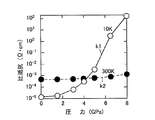
- FIG. 2 is a diagram showing the relationship between the specific resistance of CuRh 2 S 4 and the pressure.
- the vertical axis represents the specific resistance
- the horizontal axis represents the pressure applied to CuRh 2 S 4 .
- Curve k1 shows the relationship between specific resistance and pressure at an absolute temperature of 10K
- curve k2 shows the relationship between specific resistance and pressure at an absolute temperature of 300K.
- CuRh 2 S 4 becomes a superconductor at an absolute temperature of 10K or less, and maintains a superconducting state when a pressure lower than 5.3 GPa is applied at a temperature of 10K or less.
- a pressure of 3 GPa or more is applied, a transition from a superconductor to an insulator occurs.
- the pressure of GPa is the critical pressure PMI at which the superconductor transitions to the insulator.
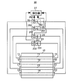
- FIG. 3 is a schematic diagram showing the configuration of the pressure detection device according to the embodiment of the present invention.
- pressure detector 30 according to the embodiment of the present invention includes container 10, superconductor thin films 11-14, electrodes 15-22, measuring instruments 23-26, detector 27, and the like. Is provided.
- the container 10 has a substantially rectangular shape.
- the inside of the container 10 is cooled to an absolute temperature of 10K or less with liquid nitrogen or the like.
- the superconductor thin films 11 to 14 are arranged in parallel in the container 10.
- the superconductor thin film 11 is made of CuRh 2 S 4 or CuIr 2 S 4 and has a critical pressure P MI 1 that makes a transition from a superconductor to an insulator.
- the superconductor thin film 12 is made of CuIr 2 S 4 to which zinc (Zn) is added, and has a critical pressure P MI 2 ( ⁇ P MI 1) for transition from the superconductor to the insulator.
- the superconductor thin film 13 is made of CuIr 2 S 4 to which Zn is added more than the superconductor thin film 12, and has a critical pressure P MI 3 ( ⁇ P MI 2) for transition from the superconductor to the insulator. .
- the superconductor thin film 14 is made of CuIr 2 S 4 to which Zn is added more than the superconductor thin film 13, and has a critical pressure P MI 4 ( ⁇ P MI 3) for transition from the superconductor to the insulator. .
- critical pressure P MI 1 consists 5.3 GPa
- critical pressure P MI 4 consists of 0.5 GPa
- Each of the electrodes 15 to 22 is made of, for example, aluminum (Al).
- the electrodes 15 to 18 are connected to one ends of the superconductor thin films 11 to 14, respectively, and the electrodes 19 to 22 are connected to the other ends of the superconductor thin films 11 to 14, respectively.
- the measuring instrument 23 is connected between the electrodes 15 and 19 through a conducting wire.
- the measuring device 24 is connected between the electrodes 16 and 20 via a conducting wire.
- the measuring instrument 25 is connected between the electrodes 17 and 21 via a conducting wire.
- the measuring device 26 is connected between the electrodes 18 and 22 via a conducting wire.
- Measuring instrument 23 includes a DC power supply 231 and an ammeter 232.
- the DC power source 231 applies a DC voltage V between the electrodes 15 and 19.
- the ammeter 232 detects the current I1 that flows through the superconductor thin film 11 when the DC power supply 231 applies the DC voltage V between the electrodes 15 and 19, and outputs the detected current I1 to the detector 27.
- the measuring instrument 24 includes a DC power supply 241 and an ammeter 242.
- the DC power source 241 applies a DC voltage V between the electrodes 16 and 20.
- the ammeter 242 detects the current I2 flowing through the superconductor thin film 12 when the DC power supply 241 applies the DC voltage V between the electrodes 16 and 20, and outputs the detected current I2 to the detector 27.
- the measuring instrument 25 includes a DC power supply 251 and an ammeter 252.
- the DC power source 251 applies a DC voltage V between the electrodes 17 and 21.
- the ammeter 252 detects the current I3 flowing through the superconductor thin film 13 when the DC power supply 251 applies the DC voltage V between the electrodes 17 and 21, and outputs the detected current I3 to the detector 27.
- the measuring instrument 26 includes a DC power supply 261 and an ammeter 262.
- the DC power supply 261 applies a DC voltage V between the electrodes 18 and 22.
- the ammeter 262 detects the current I4 flowing through the superconductor thin film 14 when the DC power supply 261 applies the DC voltage V between the electrodes 18 and 22, and outputs the detected current I4 to the detector 27.
- Detector 27 receives currents I1-I4 from ammeters 232, 242, 252, and 262, respectively. Further, the detector 27 holds a correspondence relationship between the currents I1 ⁇ I4 and the critical pressure P MI 1 ⁇ P MI 4.
- the detector 27 detects the critical pressure PMI j associated with the current Ij.
- the maximum critical pressure is detected as the pressure in the container 10.
- Detector 27 for example, when a current I2 ⁇ I4 flowing in the superconductor thin film 12 to 14 becomes "0", of the critical pressure P MI 2 ⁇ P MI 4, the maximum of the critical pressure P MI 2 chamber 10 Detect as the pressure. If the pressure P in the container 10 is in the range of P MI 2 ⁇ P ⁇ P MI 1, the superconductor thin films 12 to 14 transition from the superconductor to the insulator, so that the superconductor thin film transitioned to the insulator Currents I2 to I4 flowing through 12 to 14 are “0”. Therefore, the detector 27 detects the maximum critical pressure P MI 2 among the critical pressures P MI 2 to P MI 4 as the pressure in the container 10.
- the detector 27 detects the superconductor thin films 12 to 14 that have transitioned from the superconductor to the insulator among the superconductor thin films 11 to 14, and the critical pressure of the detected superconductor thin films 12 to 14 is detected.
- the maximum critical pressure PMI2 is detected as the pressure in the container 10.
- the detector 27 detects the pressure in the container 10 in the same manner even when the current flowing through the other superconductor thin film becomes “0”.
- the pressure detecting device 30 the temperature of the superconductor film 11 to 14 while holding the following absolute temperature 10K, the pressure applied to the superconducting thin film 11 to 14 is equal to or higher than the critical pressure P MI
- the pressure in the container 10 is detected by utilizing the characteristic of transition from a superconductor to an insulator.
- the pressure detection device 30 can detect the pressure in the container 10 while keeping the temperature in the container 10 at an absolute temperature of 10K or less.
- the pressure detection device 30 is not limited to the four superconductor thin films 11 to 14, and generally includes a plurality of superconductor thin films.
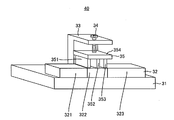
- FIG. 4 is a schematic diagram showing the configuration of the Josephson element according to the embodiment of the present invention.
- Josephson element 40 according to the embodiment of the present invention includes a base 31, a superconductor thin film 32, a support member 33, a screw 34, and a pressing member 35.
- the superconductor thin film 32 is cooled to an absolute temperature of 10K or less by liquid nitrogen or the like.
- the superconductor thin film 32 is made of CuRh 2 S 4 and has a rod shape.
- the superconductor thin film 32 is disposed on the base 31.
- the support member 33 is substantially L-shaped, and one end is fixed to the base 31.
- the support member 33 has a screw hole (not shown) for fitting with the screw 34 on the other end side.
- the screw 34 is fitted into a screw hole formed in the support member 33 and rotates clockwise to press the pressing member 35 against the superconductor thin film 32.
- the pressing member 35 is disposed in contact with an arbitrary part of the superconductor thin film 32.
- the pressing member 35 is pressed against the superconductor thin film 32 by the screw 34.
- the pressing member 35 includes projecting members 351 to 353 and a base 354.
- Each of the projecting members 351 to 353 has a substantially flat plate shape, and has the same width as the superconductor thin film 32 and a thickness of 1 ⁇ m.
- the plurality of projecting members 351 to 353 are fixed substantially perpendicular to the base 354 at intervals of 2 ⁇ m.
- the base 354 has a substantially flat plate shape, and fixes a plurality of projecting members 351 to 353.
- the base 354 is in contact with one end of the screw 34 and presses the projecting members 351 to 353 against the superconductor thin film 32 by rotating the screw 34 clockwise.
- the screw 34 rotates clockwise so that each of the projecting members 351 to 353 of the pressing member 35 applies a pressure of 100 g to the superconductor thin film 32.
- the superconductor thin film 32 is separated into superconducting layers 321 and 323 and an insulating layer 322. Then, the Josephson element 40 including the superconducting layers 321 and 323 and the insulating layer 322 is manufactured.
- a Josephson element can be manufactured using the superconductor thin film 32 made of the same material (CuRh 2 S 4 ).
- a Josephson element can be produced by controlling the pressure applied while keeping the temperature of the superconductor thin film 32 constant.
- the characteristics of the Josephson element 40 can be changed. That is, the characteristics of the Josephson element 40 itself can be changed by changing the pressure applied to the superconductor thin film 32. This property is not present in Josephson devices manufactured using different materials.
- the number of protruding members may be one.
- the pressing member 35 may be pressed against the superconductor thin film 32 using a piezoelectric element or an electrostrictive element instead of the screw 34.
- FIG. 5 is a schematic diagram showing the configuration of another Josephson element according to the embodiment of the present invention.
- the Josephson element according to the embodiment of the present invention may be a Josephson element 40A shown in FIG.
- Josephson element 40A is obtained by removing support member 33 and screw 34 of Josephson element 40 shown in FIG. 4 and replacing pressing member 35 with piezoelectric element 35A. This is the same as the Son element 40.
- the piezoelectric element 35 ⁇ / b> A is disposed on the superconductor thin film 32 in close contact with the superconductor thin film 32.
- the piezoelectric element 35A presses the superconductor thin film 32 in the thickness direction when a voltage is applied by a voltage source (not shown).
- the superconductor thin film 32 is separated into the superconducting layers 321 and 323 and the insulating layer 322, and the Josephson element 40A is manufactured.
- an electrostrictive element may be used instead of the piezoelectric element 35A.
- FIG. 6 is a schematic diagram showing a configuration of a superconducting quantum interferometer according to an embodiment of the present invention.
- superconducting quantum interferometer 50 according to the embodiment of the present invention includes superconductor thin film 51 and pressing members 52 and 53.
- the superconductor thin film 51 is cooled to an absolute temperature of 10K or less by liquid nitrogen or the like.
- the superconductor thin film 51 is made of CuRh 2 S 4 and has a ring shape.
- Each of the pressing members 52 and 53 has the same configuration as the pressing member 35 shown in FIG.
- the superconductor thin film 51 is separated into superconducting layers 511 and 513 and insulating layers 512 and 514. Then, a superconducting quantum interferometer 50 is produced.
- the insulating layer 512 is applied to a part of the superconductor thin film 51. , 514.
- a superconducting quantum interferometer can be produced using the superconductor thin film 51 made of the same material (CuRh 2 S 4 ).
- a superconducting quantum interferometer can be produced by controlling the applied pressure while keeping the temperature of the superconductor thin film 51 constant.
- the pressing members 52 and 53 may be pressed against the superconductor thin film 51 using a piezoelectric element or an electrostrictive element instead of the screw 34.
- the insulating layers 512 and 514 may be formed using the piezoelectric element 35A (or electrostrictive element).
- the applied pressure becomes equal to or higher than the critical pressure PMI , the characteristic is that a transition from a superconductor to an insulator is performed.
- the present invention is applied to a pressure detection device using a superconductor that transitions from a superconductor to an insulator while keeping the temperature constant.
- the present invention is also applied to a Josephson element using a superconductor that transitions from a superconductor to an insulator while keeping the temperature constant.
- the present invention is applied to a superconducting quantum interferometer using a superconductor that transitions from a superconductor to an insulator while keeping the temperature constant.
Landscapes
- Superconductor Devices And Manufacturing Methods Thereof (AREA)
- Measuring Fluid Pressure (AREA)
- Pressure Sensors (AREA)
Abstract
Description
Claims (9)
- 10K以下の絶対温度に保持された容器と、
前記容器内に配置され、超伝導体から絶縁体へ遷移する臨界圧力が相互に異なる複数の超伝導体薄膜と、
前記複数の超伝導体薄膜のうち、前記超伝導体から前記絶縁体へ遷移した超伝導体薄膜を検出し、その検出した超伝導体薄膜の前記臨界圧力のうち最大の臨界圧力を前記容器内の圧力として検出する検出器とを備える圧力検出装置。 - 前記複数の超伝導体薄膜に対応して設けられ、各々が対応する超伝導体薄膜の一方端に接続された複数の第1の電極と、
前記複数の超伝導体薄膜に対応して設けられ、各々が対応する超伝導体薄膜の他方端に接続された複数の第2の電極とをさらに備え、
前記検出器は、各超伝導体薄膜の両端に配置された第1および第2の電極間に流れる電流を検出することにより、前記複数の超伝導体薄膜のうち、前記超伝導体から前記絶縁体へ遷移した超伝導体薄膜を検出する、請求の範囲第1項に記載の圧力検出装置。 - 前記複数の超伝導体薄膜は、添加物量が相互に異なる複数のCuIr2S4からなる、請求の範囲第1項に記載の圧力検出装置。
- 10K以下の絶対温度に保持され、CuRh2S4からなる超伝導体薄膜と、
前記超伝導体薄膜の一部に超伝導体から絶縁体へ遷移する臨界圧力以上の圧力を印加する圧力印加器とを備えるジョセフソン素子。 - 前記圧力印加器は、
複数の突起部材と、
前記複数の突起部材を前記超伝導体薄膜の一部に押し付ける押付部材とを含む、請求の範囲第4項に記載のジョセフソン素子。 - 前記押付部材は、電歪素子または圧電素子からなる、請求の範囲第5項に記載のジョセフソン素子。
- 前記圧力印加器は、前記超伝導体薄膜の一部に接して配置された電歪素子からなる、請求の範囲第5項に記載のジョセフソン素子。
- 輪形状を有するとともに、10K以下の絶対温度に保持されたCuRh2S4からなる超伝導体薄膜と、
前記超伝導体薄膜の第1の一部分に超伝導体から絶縁体へ遷移する臨界圧力以上の圧力を印加する第1の圧力印加器と、
前記超伝導体薄膜の前記第1の一部分と異なる第2の一部分に前記臨界圧力以上の圧力を印加する第2の圧力印加器とを備える超伝導量子干渉計。 - 前記第1および第2の圧力印加器の各々は、
複数の突起部材と、
前記複数の突起部材を前記超伝導体薄膜の一部に押し付ける押付部材とを含む、請求の範囲第8項に記載の超伝導量子干渉計。
Priority Applications (3)
| Application Number | Priority Date | Filing Date | Title |
|---|---|---|---|
| US12/601,790 US8338821B2 (en) | 2008-07-31 | 2008-07-31 | Pressure detection apparatus, Josephson device, and superconducting quantum interference device that include superconductor thin film that undergoes transition from superconductor to insulator by pressure |
| JP2009525838A JP4394751B1 (ja) | 2008-07-31 | 2008-07-31 | 圧力によって超伝導体から絶縁体へ遷移する超伝導体薄膜を用いた圧力検出装置 |
| PCT/JP2008/002069 WO2010013294A1 (ja) | 2008-07-31 | 2008-07-31 | 圧力によって超伝導体から絶縁体へ遷移する超伝導体薄膜を用いた圧力検出装置、ジョセフソン素子および超伝導量子干渉計 |
Applications Claiming Priority (1)
| Application Number | Priority Date | Filing Date | Title |
|---|---|---|---|
| PCT/JP2008/002069 WO2010013294A1 (ja) | 2008-07-31 | 2008-07-31 | 圧力によって超伝導体から絶縁体へ遷移する超伝導体薄膜を用いた圧力検出装置、ジョセフソン素子および超伝導量子干渉計 |
Publications (1)
| Publication Number | Publication Date |
|---|---|
| WO2010013294A1 true WO2010013294A1 (ja) | 2010-02-04 |
Family
ID=41591547
Family Applications (1)
| Application Number | Title | Priority Date | Filing Date |
|---|---|---|---|
| PCT/JP2008/002069 Ceased WO2010013294A1 (ja) | 2008-07-31 | 2008-07-31 | 圧力によって超伝導体から絶縁体へ遷移する超伝導体薄膜を用いた圧力検出装置、ジョセフソン素子および超伝導量子干渉計 |
Country Status (3)
| Country | Link |
|---|---|
| US (1) | US8338821B2 (ja) |
| JP (1) | JP4394751B1 (ja) |
| WO (1) | WO2010013294A1 (ja) |
Cited By (1)
| Publication number | Priority date | Publication date | Assignee | Title |
|---|---|---|---|---|
| KR20150046053A (ko) * | 2012-08-21 | 2015-04-29 | 필립모리스 프로덕츠 에스.에이. | 벤틸레이터 에어로졸 전달 시스템 |
Families Citing this family (19)
| Publication number | Priority date | Publication date | Assignee | Title |
|---|---|---|---|---|
| WO2019160573A2 (en) | 2017-05-16 | 2019-08-22 | PsiQuantum Corp. | Superconducting signal amplifier |
| WO2019160572A2 (en) | 2017-05-16 | 2019-08-22 | PsiQuantum Corp. | Gated superconducting photon detector |
| US10586910B2 (en) | 2017-07-28 | 2020-03-10 | PsiQuantum Corp. | Superconductor-based transistor |
| US10374611B2 (en) | 2017-10-05 | 2019-08-06 | PsiQuantum Corp. | Superconducting logic components |
| US10461445B2 (en) | 2017-11-13 | 2019-10-29 | PsiQuantum Corp. | Methods and devices for impedance multiplication |
| WO2019157077A1 (en) | 2018-02-06 | 2019-08-15 | PsiQuantum Corp. | Superconducting photon detector |
| WO2019160869A1 (en) | 2018-02-14 | 2019-08-22 | PsiQuantum Corp. | Superconducting logic components |
| US11313719B2 (en) | 2018-05-01 | 2022-04-26 | PsiQuantum Corp. | Photon number resolving superconducting detector |
| US10984857B2 (en) | 2018-08-16 | 2021-04-20 | PsiQuantum Corp. | Superconductive memory cells and devices |
| US10573800B1 (en) * | 2018-08-21 | 2020-02-25 | PsiQuantum Corp. | Superconductor-to-insulator devices |
| US11101215B2 (en) | 2018-09-19 | 2021-08-24 | PsiQuantum Corp. | Tapered connectors for superconductor circuits |
| US11719653B1 (en) | 2018-09-21 | 2023-08-08 | PsiQuantum Corp. | Methods and systems for manufacturing superconductor devices |
| US10944403B2 (en) | 2018-10-27 | 2021-03-09 | PsiQuantum Corp. | Superconducting field-programmable gate array |
| US11289590B1 (en) | 2019-01-30 | 2022-03-29 | PsiQuantum Corp. | Thermal diode switch |
| US11569816B1 (en) | 2019-04-10 | 2023-01-31 | PsiQuantum Corp. | Superconducting switch |
| US11009387B2 (en) | 2019-04-16 | 2021-05-18 | PsiQuantum Corp. | Superconducting nanowire single photon detector and method of fabrication thereof |
| US11380731B1 (en) | 2019-09-26 | 2022-07-05 | PsiQuantum Corp. | Superconducting device with asymmetric impedance |
| US11585695B1 (en) | 2019-10-21 | 2023-02-21 | PsiQuantum Corp. | Self-triaging photon detector |
| US11994426B1 (en) | 2019-11-13 | 2024-05-28 | PsiQuantum Corp. | Scalable photon number resolving photon detector |
Citations (5)
| Publication number | Priority date | Publication date | Assignee | Title |
|---|---|---|---|---|
| JPS63232381A (ja) * | 1987-03-19 | 1988-09-28 | Fujitsu Ltd | 超伝導素子 |
| JPH0191480A (ja) * | 1987-06-17 | 1989-04-11 | Nippon Telegr & Teleph Corp <Ntt> | 電流制御素子及び電流制御方法 |
| JPH0341332A (ja) * | 1989-07-07 | 1991-02-21 | Sanyo Electric Co Ltd | 超電導圧力センサ |
| JPH065934A (ja) * | 1992-06-16 | 1994-01-14 | Seiko Epson Corp | 超電導体装置 |
| JP2000351632A (ja) * | 1999-04-09 | 2000-12-19 | Natl Res Inst For Metals | 硫化物スピネル系超伝導物質 |
Family Cites Families (7)
| Publication number | Priority date | Publication date | Assignee | Title |
|---|---|---|---|---|
| JPS63263781A (ja) | 1987-04-22 | 1988-10-31 | Nec Corp | セラミツク超伝導体ジヨセフソン接合の製造方法 |
| JPS6490573A (en) | 1987-10-01 | 1989-04-07 | Olympus Optical Co | Superconducting element |
| JPH02260474A (ja) | 1989-03-31 | 1990-10-23 | Canon Inc | 平面型マイクロブリッジジョセフソン接合素子及びその特性制御法 |
| JP2674680B2 (ja) | 1994-02-23 | 1997-11-12 | 宇都宮大学長 | 超伝導超格子結晶デバイス |
| US6109113A (en) * | 1998-06-11 | 2000-08-29 | Delco Electronics Corp. | Silicon micromachined capacitive pressure sensor and method of manufacture |
| JP2000004052A (ja) * | 1998-06-15 | 2000-01-07 | Fuji Electric Co Ltd | 超電導装置 |
| JP5152549B2 (ja) | 2006-07-20 | 2013-02-27 | 独立行政法人科学技術振興機構 | ジョセフソン接合及びジョセフソンデバイス |
-
2008
- 2008-07-31 WO PCT/JP2008/002069 patent/WO2010013294A1/ja not_active Ceased
- 2008-07-31 US US12/601,790 patent/US8338821B2/en not_active Expired - Fee Related
- 2008-07-31 JP JP2009525838A patent/JP4394751B1/ja not_active Expired - Fee Related
Patent Citations (5)
| Publication number | Priority date | Publication date | Assignee | Title |
|---|---|---|---|---|
| JPS63232381A (ja) * | 1987-03-19 | 1988-09-28 | Fujitsu Ltd | 超伝導素子 |
| JPH0191480A (ja) * | 1987-06-17 | 1989-04-11 | Nippon Telegr & Teleph Corp <Ntt> | 電流制御素子及び電流制御方法 |
| JPH0341332A (ja) * | 1989-07-07 | 1991-02-21 | Sanyo Electric Co Ltd | 超電導圧力センサ |
| JPH065934A (ja) * | 1992-06-16 | 1994-01-14 | Seiko Epson Corp | 超電導体装置 |
| JP2000351632A (ja) * | 1999-04-09 | 2000-12-19 | Natl Res Inst For Metals | 硫化物スピネル系超伝導物質 |
Cited By (2)
| Publication number | Priority date | Publication date | Assignee | Title |
|---|---|---|---|---|
| KR20150046053A (ko) * | 2012-08-21 | 2015-04-29 | 필립모리스 프로덕츠 에스.에이. | 벤틸레이터 에어로졸 전달 시스템 |
| KR102163958B1 (ko) | 2012-08-21 | 2020-10-13 | 필립모리스 프로덕츠 에스.에이. | 벤틸레이터 에어로졸 전달 시스템 |
Also Published As
| Publication number | Publication date |
|---|---|
| JP4394751B1 (ja) | 2010-01-06 |
| US8338821B2 (en) | 2012-12-25 |
| US20100171098A1 (en) | 2010-07-08 |
| JPWO2010013294A1 (ja) | 2012-01-05 |
Similar Documents
| Publication | Publication Date | Title |
|---|---|---|
| JP4394751B1 (ja) | 圧力によって超伝導体から絶縁体へ遷移する超伝導体薄膜を用いた圧力検出装置 | |
| Dhoot et al. | Large electric field effect in electrolyte-gated manganites | |
| Yang et al. | Solid‐state electrochemical thermal transistors | |
| Raj et al. | Self-powered ferroelectric NTC thermistor based on bismuth titanate | |
| Li et al. | Symmetry breaking and anomalous conductivity in a double-moiré superlattice | |
| KR102271962B1 (ko) | 비스무트 티타네이트 기반 연성 강유전체 서미스터 장치 및 그 제조방법, 비스무트 티타네이트 적용 복합 필름-기반 압전 나노제너레이터 및 그 제조방법, 상기 장치를 적용하는 자가 발전 구조의 실시간 환경 온도 모니터링 시스템 | |
| Mutiso et al. | Resistive switching in silver/polystyrene/silver nano-gap devices | |
| Matthey et al. | Field-effect experiments in NdBa 2 Cu 3 O 7− δ ultrathin films using a SrTiO 3 single-crystal gate insulator | |
| Zhao et al. | Magnetoresistance behavior of conducting filaments in resistive-switching NiO with different resistance states | |
| Perlman et al. | Production and charge decay of film electrets | |
| US20070164272A1 (en) | Three-terminal electrical bistable devices | |
| Peck et al. | Response of the double-layer capacitance of a high-temperature superconductor/fluid electrolyte interface to the onset of superconductivity | |
| Park et al. | Electrostatic Clutches Based on Ionomer Heterojunctions for Low‐Voltage Switching of Stiffness and Strength | |
| JP4460021B2 (ja) | 圧力によって超伝導体から絶縁体へ遷移する超伝導体薄膜を用いたジョセフソン素子および超伝導量子干渉計 | |
| JP5569836B2 (ja) | ペロブスカイト型酸化物の相転移誘起方法、電子機能素子材料として用いられるペロブスカイト型酸化物、ペロブスカイト型酸化物を用いた電子機能素子及び電子装置 | |
| Souchier et al. | First evidence of resistive switching in polycrystalline GaV4S8 thin layers | |
| Naidyuk et al. | Switchable domains in point contacts based on transition metal tellurides | |
| Noriega et al. | Characterization system for research on energy storage capacitors | |
| Tayyab et al. | Synergetic effect of piezo-triboelectric mechanism for high-performance nanogenerators | |
| Monteverde et al. | Pressure control of conducting channels in single-wall carbon nanotube networks | |
| Yamauchi et al. | Hall effect of iodine in high pressure | |
| Noskin et al. | Growth of NbO2 by molecular-beam epitaxy and characterization of its metal-insulator transition | |
| JP6813844B2 (ja) | トンネル接合素子及び不揮発性メモリ素子 | |
| CN107946457B (zh) | 一种电致电阻转变功能器件的处理方法及一种超大磁电阻器件 | |
| Zhang et al. | Nonvolatile resistive switching in Co doped amorphous carbon film |
Legal Events
| Date | Code | Title | Description |
|---|---|---|---|
| ENP | Entry into the national phase |
Ref document number: 2009525838 Country of ref document: JP Kind code of ref document: A |
|
| WWE | Wipo information: entry into national phase |
Ref document number: 12601790 Country of ref document: US |
|
| 121 | Ep: the epo has been informed by wipo that ep was designated in this application |
Ref document number: 08790333 Country of ref document: EP Kind code of ref document: A1 |
|
| NENP | Non-entry into the national phase |
Ref country code: DE |
|
| 122 | Ep: pct application non-entry in european phase |
Ref document number: 08790333 Country of ref document: EP Kind code of ref document: A1 |