WO2010010792A1 - 導電性パターン形成方法及び有機薄膜トランジスタ - Google Patents
導電性パターン形成方法及び有機薄膜トランジスタ Download PDFInfo
- Publication number
- WO2010010792A1 WO2010010792A1 PCT/JP2009/061840 JP2009061840W WO2010010792A1 WO 2010010792 A1 WO2010010792 A1 WO 2010010792A1 JP 2009061840 W JP2009061840 W JP 2009061840W WO 2010010792 A1 WO2010010792 A1 WO 2010010792A1
- Authority
- WO
- WIPO (PCT)
- Prior art keywords
- conductive pattern
- general formula
- substrate
- compound represented
- photomask
- Prior art date
- Legal status (The legal status is an assumption and is not a legal conclusion. Google has not performed a legal analysis and makes no representation as to the accuracy of the status listed.)
- Ceased
Links
Images
Classifications
-
- C—CHEMISTRY; METALLURGY
- C23—COATING METALLIC MATERIAL; COATING MATERIAL WITH METALLIC MATERIAL; CHEMICAL SURFACE TREATMENT; DIFFUSION TREATMENT OF METALLIC MATERIAL; COATING BY VACUUM EVAPORATION, BY SPUTTERING, BY ION IMPLANTATION OR BY CHEMICAL VAPOUR DEPOSITION, IN GENERAL; INHIBITING CORROSION OF METALLIC MATERIAL OR INCRUSTATION IN GENERAL
- C23C—COATING METALLIC MATERIAL; COATING MATERIAL WITH METALLIC MATERIAL; SURFACE TREATMENT OF METALLIC MATERIAL BY DIFFUSION INTO THE SURFACE, BY CHEMICAL CONVERSION OR SUBSTITUTION; COATING BY VACUUM EVAPORATION, BY SPUTTERING, BY ION IMPLANTATION OR BY CHEMICAL VAPOUR DEPOSITION, IN GENERAL
- C23C18/00—Chemical coating by decomposition of either liquid compounds or solutions of the coating forming compounds, without leaving reaction products of surface material in the coating; Contact plating
- C23C18/16—Chemical coating by decomposition of either liquid compounds or solutions of the coating forming compounds, without leaving reaction products of surface material in the coating; Contact plating by reduction or substitution, e.g. electroless plating
- C23C18/1601—Process or apparatus
- C23C18/1603—Process or apparatus coating on selected surface areas
- C23C18/1607—Process or apparatus coating on selected surface areas by direct patterning
- C23C18/1608—Process or apparatus coating on selected surface areas by direct patterning from pretreatment step, i.e. selective pre-treatment
-
- C—CHEMISTRY; METALLURGY
- C23—COATING METALLIC MATERIAL; COATING MATERIAL WITH METALLIC MATERIAL; CHEMICAL SURFACE TREATMENT; DIFFUSION TREATMENT OF METALLIC MATERIAL; COATING BY VACUUM EVAPORATION, BY SPUTTERING, BY ION IMPLANTATION OR BY CHEMICAL VAPOUR DEPOSITION, IN GENERAL; INHIBITING CORROSION OF METALLIC MATERIAL OR INCRUSTATION IN GENERAL
- C23C—COATING METALLIC MATERIAL; COATING MATERIAL WITH METALLIC MATERIAL; SURFACE TREATMENT OF METALLIC MATERIAL BY DIFFUSION INTO THE SURFACE, BY CHEMICAL CONVERSION OR SUBSTITUTION; COATING BY VACUUM EVAPORATION, BY SPUTTERING, BY ION IMPLANTATION OR BY CHEMICAL VAPOUR DEPOSITION, IN GENERAL
- C23C18/00—Chemical coating by decomposition of either liquid compounds or solutions of the coating forming compounds, without leaving reaction products of surface material in the coating; Contact plating
- C23C18/16—Chemical coating by decomposition of either liquid compounds or solutions of the coating forming compounds, without leaving reaction products of surface material in the coating; Contact plating by reduction or substitution, e.g. electroless plating
- C23C18/1601—Process or apparatus
- C23C18/1603—Process or apparatus coating on selected surface areas
- C23C18/1607—Process or apparatus coating on selected surface areas by direct patterning
- C23C18/1612—Process or apparatus coating on selected surface areas by direct patterning through irradiation means
-
- C—CHEMISTRY; METALLURGY
- C23—COATING METALLIC MATERIAL; COATING MATERIAL WITH METALLIC MATERIAL; CHEMICAL SURFACE TREATMENT; DIFFUSION TREATMENT OF METALLIC MATERIAL; COATING BY VACUUM EVAPORATION, BY SPUTTERING, BY ION IMPLANTATION OR BY CHEMICAL VAPOUR DEPOSITION, IN GENERAL; INHIBITING CORROSION OF METALLIC MATERIAL OR INCRUSTATION IN GENERAL
- C23C—COATING METALLIC MATERIAL; COATING MATERIAL WITH METALLIC MATERIAL; SURFACE TREATMENT OF METALLIC MATERIAL BY DIFFUSION INTO THE SURFACE, BY CHEMICAL CONVERSION OR SUBSTITUTION; COATING BY VACUUM EVAPORATION, BY SPUTTERING, BY ION IMPLANTATION OR BY CHEMICAL VAPOUR DEPOSITION, IN GENERAL
- C23C18/00—Chemical coating by decomposition of either liquid compounds or solutions of the coating forming compounds, without leaving reaction products of surface material in the coating; Contact plating
- C23C18/16—Chemical coating by decomposition of either liquid compounds or solutions of the coating forming compounds, without leaving reaction products of surface material in the coating; Contact plating by reduction or substitution, e.g. electroless plating
- C23C18/18—Pretreatment of the material to be coated
- C23C18/1851—Pretreatment of the material to be coated of surfaces of non-metallic or semiconducting in organic material
- C23C18/1862—Pretreatment of the material to be coated of surfaces of non-metallic or semiconducting in organic material by radiant energy
- C23C18/1868—Radiation, e.g. UV, laser
-
- C—CHEMISTRY; METALLURGY
- C23—COATING METALLIC MATERIAL; COATING MATERIAL WITH METALLIC MATERIAL; CHEMICAL SURFACE TREATMENT; DIFFUSION TREATMENT OF METALLIC MATERIAL; COATING BY VACUUM EVAPORATION, BY SPUTTERING, BY ION IMPLANTATION OR BY CHEMICAL VAPOUR DEPOSITION, IN GENERAL; INHIBITING CORROSION OF METALLIC MATERIAL OR INCRUSTATION IN GENERAL
- C23C—COATING METALLIC MATERIAL; COATING MATERIAL WITH METALLIC MATERIAL; SURFACE TREATMENT OF METALLIC MATERIAL BY DIFFUSION INTO THE SURFACE, BY CHEMICAL CONVERSION OR SUBSTITUTION; COATING BY VACUUM EVAPORATION, BY SPUTTERING, BY ION IMPLANTATION OR BY CHEMICAL VAPOUR DEPOSITION, IN GENERAL
- C23C18/00—Chemical coating by decomposition of either liquid compounds or solutions of the coating forming compounds, without leaving reaction products of surface material in the coating; Contact plating
- C23C18/16—Chemical coating by decomposition of either liquid compounds or solutions of the coating forming compounds, without leaving reaction products of surface material in the coating; Contact plating by reduction or substitution, e.g. electroless plating
- C23C18/18—Pretreatment of the material to be coated
- C23C18/1851—Pretreatment of the material to be coated of surfaces of non-metallic or semiconducting in organic material
- C23C18/1872—Pretreatment of the material to be coated of surfaces of non-metallic or semiconducting in organic material by chemical pretreatment
- C23C18/1875—Pretreatment of the material to be coated of surfaces of non-metallic or semiconducting in organic material by chemical pretreatment only one step pretreatment
- C23C18/1882—Use of organic or inorganic compounds other than metals, e.g. activation, sensitisation with polymers
-
- C—CHEMISTRY; METALLURGY
- C23—COATING METALLIC MATERIAL; COATING MATERIAL WITH METALLIC MATERIAL; CHEMICAL SURFACE TREATMENT; DIFFUSION TREATMENT OF METALLIC MATERIAL; COATING BY VACUUM EVAPORATION, BY SPUTTERING, BY ION IMPLANTATION OR BY CHEMICAL VAPOUR DEPOSITION, IN GENERAL; INHIBITING CORROSION OF METALLIC MATERIAL OR INCRUSTATION IN GENERAL
- C23C—COATING METALLIC MATERIAL; COATING MATERIAL WITH METALLIC MATERIAL; SURFACE TREATMENT OF METALLIC MATERIAL BY DIFFUSION INTO THE SURFACE, BY CHEMICAL CONVERSION OR SUBSTITUTION; COATING BY VACUUM EVAPORATION, BY SPUTTERING, BY ION IMPLANTATION OR BY CHEMICAL VAPOUR DEPOSITION, IN GENERAL
- C23C18/00—Chemical coating by decomposition of either liquid compounds or solutions of the coating forming compounds, without leaving reaction products of surface material in the coating; Contact plating
- C23C18/16—Chemical coating by decomposition of either liquid compounds or solutions of the coating forming compounds, without leaving reaction products of surface material in the coating; Contact plating by reduction or substitution, e.g. electroless plating
- C23C18/31—Coating with metals
-
- G—PHYSICS
- G03—PHOTOGRAPHY; CINEMATOGRAPHY; ANALOGOUS TECHNIQUES USING WAVES OTHER THAN OPTICAL WAVES; ELECTROGRAPHY; HOLOGRAPHY
- G03F—PHOTOMECHANICAL PRODUCTION OF TEXTURED OR PATTERNED SURFACES, e.g. FOR PRINTING, FOR PROCESSING OF SEMICONDUCTOR DEVICES; MATERIALS THEREFOR; ORIGINALS THEREFOR; APPARATUS SPECIALLY ADAPTED THEREFOR
- G03F1/00—Originals for photomechanical production of textured or patterned surfaces, e.g., masks, photo-masks, reticles; Mask blanks or pellicles therefor; Containers specially adapted therefor; Preparation thereof
- G03F1/60—Substrates
-
- G—PHYSICS
- G03—PHOTOGRAPHY; CINEMATOGRAPHY; ANALOGOUS TECHNIQUES USING WAVES OTHER THAN OPTICAL WAVES; ELECTROGRAPHY; HOLOGRAPHY
- G03F—PHOTOMECHANICAL PRODUCTION OF TEXTURED OR PATTERNED SURFACES, e.g. FOR PRINTING, FOR PROCESSING OF SEMICONDUCTOR DEVICES; MATERIALS THEREFOR; ORIGINALS THEREFOR; APPARATUS SPECIALLY ADAPTED THEREFOR
- G03F7/00—Photomechanical, e.g. photolithographic, production of textured or patterned surfaces, e.g. printing surfaces; Materials therefor, e.g. comprising photoresists; Apparatus specially adapted therefor
- G03F7/004—Photosensitive materials
- G03F7/075—Silicon-containing compounds
- G03F7/0755—Non-macromolecular compounds containing Si-O, Si-C or Si-N bonds
-
- H—ELECTRICITY
- H05—ELECTRIC TECHNIQUES NOT OTHERWISE PROVIDED FOR
- H05K—PRINTED CIRCUITS; CASINGS OR CONSTRUCTIONAL DETAILS OF ELECTRIC APPARATUS; MANUFACTURE OF ASSEMBLAGES OF ELECTRICAL COMPONENTS
- H05K3/00—Apparatus or processes for manufacturing printed circuits
- H05K3/10—Apparatus or processes for manufacturing printed circuits in which conductive material is applied to the insulating support in such a manner as to form the desired conductive pattern
- H05K3/18—Apparatus or processes for manufacturing printed circuits in which conductive material is applied to the insulating support in such a manner as to form the desired conductive pattern using precipitation techniques to apply the conductive material
- H05K3/181—Apparatus or processes for manufacturing printed circuits in which conductive material is applied to the insulating support in such a manner as to form the desired conductive pattern using precipitation techniques to apply the conductive material by electroless plating
- H05K3/182—Apparatus or processes for manufacturing printed circuits in which conductive material is applied to the insulating support in such a manner as to form the desired conductive pattern using precipitation techniques to apply the conductive material by electroless plating characterised by the patterning method
- H05K3/185—Apparatus or processes for manufacturing printed circuits in which conductive material is applied to the insulating support in such a manner as to form the desired conductive pattern using precipitation techniques to apply the conductive material by electroless plating characterised by the patterning method by making a catalytic pattern by photo-imaging
-
- H—ELECTRICITY
- H10—SEMICONDUCTOR DEVICES; ELECTRIC SOLID-STATE DEVICES NOT OTHERWISE PROVIDED FOR
- H10K—ORGANIC ELECTRIC SOLID-STATE DEVICES
- H10K10/00—Organic devices specially adapted for rectifying, amplifying, oscillating or switching; Organic capacitors or resistors having potential barriers
- H10K10/80—Constructional details
- H10K10/82—Electrodes
-
- H—ELECTRICITY
- H10—SEMICONDUCTOR DEVICES; ELECTRIC SOLID-STATE DEVICES NOT OTHERWISE PROVIDED FOR
- H10K—ORGANIC ELECTRIC SOLID-STATE DEVICES
- H10K71/00—Manufacture or treatment specially adapted for the organic devices covered by this subclass
- H10K71/621—Providing a shape to conductive layers, e.g. patterning or selective deposition
-
- G—PHYSICS
- G03—PHOTOGRAPHY; CINEMATOGRAPHY; ANALOGOUS TECHNIQUES USING WAVES OTHER THAN OPTICAL WAVES; ELECTROGRAPHY; HOLOGRAPHY
- G03F—PHOTOMECHANICAL PRODUCTION OF TEXTURED OR PATTERNED SURFACES, e.g. FOR PRINTING, FOR PROCESSING OF SEMICONDUCTOR DEVICES; MATERIALS THEREFOR; ORIGINALS THEREFOR; APPARATUS SPECIALLY ADAPTED THEREFOR
- G03F7/00—Photomechanical, e.g. photolithographic, production of textured or patterned surfaces, e.g. printing surfaces; Materials therefor, e.g. comprising photoresists; Apparatus specially adapted therefor
- G03F7/26—Processing photosensitive materials; Apparatus therefor
- G03F7/40—Treatment after imagewise removal, e.g. baking
- G03F7/405—Treatment with inorganic or organometallic reagents after imagewise removal
-
- H—ELECTRICITY
- H05—ELECTRIC TECHNIQUES NOT OTHERWISE PROVIDED FOR
- H05K—PRINTED CIRCUITS; CASINGS OR CONSTRUCTIONAL DETAILS OF ELECTRIC APPARATUS; MANUFACTURE OF ASSEMBLAGES OF ELECTRICAL COMPONENTS
- H05K3/00—Apparatus or processes for manufacturing printed circuits
- H05K3/38—Improvement of the adhesion between the insulating substrate and the metal
- H05K3/389—Improvement of the adhesion between the insulating substrate and the metal by the use of a coupling agent, e.g. silane
-
- H—ELECTRICITY
- H10—SEMICONDUCTOR DEVICES; ELECTRIC SOLID-STATE DEVICES NOT OTHERWISE PROVIDED FOR
- H10K—ORGANIC ELECTRIC SOLID-STATE DEVICES
- H10K10/00—Organic devices specially adapted for rectifying, amplifying, oscillating or switching; Organic capacitors or resistors having potential barriers
- H10K10/40—Organic transistors
- H10K10/46—Field-effect transistors, e.g. organic thin-film transistors [OTFT]
- H10K10/462—Insulated gate field-effect transistors [IGFETs]
- H10K10/464—Lateral top-gate IGFETs comprising only a single gate
-
- H—ELECTRICITY
- H10—SEMICONDUCTOR DEVICES; ELECTRIC SOLID-STATE DEVICES NOT OTHERWISE PROVIDED FOR
- H10K—ORGANIC ELECTRIC SOLID-STATE DEVICES
- H10K10/00—Organic devices specially adapted for rectifying, amplifying, oscillating or switching; Organic capacitors or resistors having potential barriers
- H10K10/40—Organic transistors
- H10K10/46—Field-effect transistors, e.g. organic thin-film transistors [OTFT]
- H10K10/462—Insulated gate field-effect transistors [IGFETs]
- H10K10/466—Lateral bottom-gate IGFETs comprising only a single gate
Definitions
- the present invention relates to a novel conductive pattern forming method and an organic thin film transistor.
- a resist layer is laminated on a substrate on which a conductive layer is formed, irradiated with light through a photomask having a desired pattern, and then developed. Thereafter, a photolithographic method for removing an unnecessary resist layer has been performed.
- this photolithographic method is troublesome because it requires a large number of steps, and there is also a problem in terms of cost. Further, the disposal of the removed resist layer has a problem in that it has a burden on the environment. .
- Patent Document 1 a monomolecular film made of a long-chain alkyl-based silane coupling agent is formed on a substrate, and then exposed in a pattern with a Xe excimer lamp.
- a method of forming a conductive pattern by partially decomposing and using a difference in adhesion to metal between a region where the monomolecular film remains and a region where the monomolecular film is decomposed has been studied.
- the inventor has a merit in that a vacuum process is not used, but a lamp having a wavelength of less than 300 nm is used for decomposition of a monomolecular film. Since it is necessary to use the device, it has been found that there are many limitations on the device, and there are many adverse effects on the material.
- Patent Documents 2 and 3 methods for decomposing organic molecules using the photocatalytic action of titanium dioxide are studied.
- the methods described in Patent Documents 2 and 3 have the disadvantage that the adhesion of the conductive pattern decreases as the resolution is increased because the silane coupling agent is excessively decomposed during pattern formation. It was.
- organic thin film transistors Organic Thin Film Transistors: OTFTs
- OTFTs Organic Thin Film Transistors
- An organic thin film transistor is an example of an application example of the conductive pattern forming method of the present invention.
- the organic thin film transistor has substantially the same structure as the silicon thin film transistor, but there is a difference that an organic material is used instead of silicon in the semiconductor active layer region.
- Organic thin-film transistors can be manufactured by inkjet method, printing method, etc. without using a vacuum device in terms of manufacturing process, so they are simpler and less expensive than silicon TFTs, are not broken by impact, and can be bent or folded. This is advantageous in that it is suitable for electronic circuit boards. Especially when it is necessary to manufacture devices on a large area, and when a low process temperature is required, it is effective for products to be bent, so matrix drive elements for large displays, organic EL and electronic paper drive elements As expected, each company is developing.
- the operating principle of the organic thin film transistor is to control the resistance by voltage, to control the gate voltage, and to generate an accumulation layer in the carrier on the contact surface between the organic semiconductor and the insulating layer by the action of the insulating layer. To control the conduction current between the two ohmic contacts.
- the present invention has been made in view of the above problems, and its purpose is to provide a conductive pattern forming method and device characteristics that are excellent in adhesion between the substrate and the conductive pattern by a simple process and have high reproducibility of fine lines.
- An organic thin film transistor is provided.
- a process comprising treating a substrate surface with a compound represented by the following general formula (1), a step of decomposing the compound represented by the general formula (1) by photocatalysis, and a plating step Pattern formation method.
- R represents an alkyl group having 8 or less carbon atoms
- A represents an alkoxy group or a halogen atom
- B represents a substituent containing an SH group
- n represents an integer of 0 to 2.
- the present invention it was possible to provide a conductive pattern forming method having excellent adhesion between a substrate and a conductive pattern, a high reproducibility of fine lines, and an organic thin film transistor with good device characteristics by a simple process.
- the present inventor is represented by the general formula (1) by a step of treating the substrate surface with a compound represented by the general formula (1) and a photocatalytic action. It has been found that a conductive pattern forming method including a step of decomposing a compound and a plating step including a plating step can provide a conductive pattern forming method that has excellent adhesion between the substrate and the conductive pattern and a high reproducibility of fine lines by a simple process. It was.
- the organic thin film transistor fabricated using this conductive pattern forming method is an organic thin film transistor having good element characteristics.
- the reason why the conductive pattern forming method of the present invention has excellent adhesion between the substrate and the conductive pattern and high reproducibility of fine lines is as follows. 1. Use of a compound having a photocatalytic action makes the exposure wavelength longer. 2. an adjacent SH group is present in the vicinity; It is mentioned that the density of the silane coupling agent per unit area is high.
- R represents an alkyl group having 8 or less carbon atoms, preferably a lower alkyl group having 1 to 4 carbon atoms.
- A represents an alkoxy group or a halogen atom
- the alkoxy group is, for example, a lower alkoxy group (1 to 4 carbon atoms) such as methoxy, ethoxy, propoxy, butoxy and the like, and methoxy and ethoxy groups are particularly preferable.
- the alkoxy group may have a substituent.
- halogen atoms preferred is a chlorine atom.
- B represents a substituent containing an SH group and may be an aliphatic or (hetero) aromatic group containing at least one, preferably two or more mercapto groups in its structure.
- N represents an integer of 0-2.
- the compound represented by the general formula (1) has a triazine ring, an adjacent SH group is present in the vicinity, and electrons are efficiently transferred and high sensitivity is obtained. Further, the density of the silane coupling agent per unit area Is preferable because the adhesion is improved.
- Examples of the compound represented by the general formula (1) include the following.
- A-1 Triethoxysilyl-propylamino-triazine-dithiol
- A-2 ⁇ -mercaptopropyl-trimethoxysilane
- A-3 3-mercaptopropylmethyldimethoxysilane
- A-4 Mercaptopropyltriethoxysilane
- A-5 ⁇ -mercaptopropylmethyldimethoxysilane
- A-6 ⁇ -mercaptopropyl-trichlorosilane
- compounds having a triazine ring are particularly preferred.
- A-1 represents ⁇ - It can be easily obtained by subjecting propyltriethoxysilane and the corresponding mercaptoamine, in this case, 1-amino-3,5-dimercaptotriazine (described in JP-A No. 2001-316872, etc.) to a condensation reaction.
- the conductive pattern forming method of the present invention comprises a step of treating with the compound represented by the general formula (1), a step of decomposing the compound represented by the general formula (1) by photocatalysis, and a plating step. It is characterized by including.
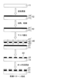
- FIG. 1 is a process diagram showing the conductive pattern forming method of the present invention.
- the substrate 11 After the substrate 11 is subjected to corona discharge treatment, it is immersed in a solution of the compound represented by the general formula (1) at room temperature, heated and dried, and the layer 21 containing the compound represented by the general formula (1) is formed.
- the base material 12 which has is obtained.
- a dispersion having a photocatalytic compound such as titanium dioxide is applied on the surface of the quartz glass 41 and baked to form a titanium dioxide layer 42.
- a Cr layer is formed on the titanium dioxide layer 42 by sputtering. Then, only the Cr layer is etched by a photolithographic method to form a pattern composed of the Cr layer 43, and the photomask 40 is obtained.
- the distance between the surface of the substrate 12 treated with the aqueous solution of the compound represented by the general formula (1) and the titanium dioxide layer 42 of the photomask 40 is set to 50 nm, for example, and exposure is performed using, for example, a high-pressure mercury lamp. .
- the region irradiated with light is represented by the region 22 in which the compound represented by the general formula (1) is decomposed by the active oxygen generated by the photocatalysis, and the region represented by the general formula (1) without being irradiated with light.
- a region 21 in which the compound to be left is left is formed.
- a liquid containing a compound represented by the general formula (1) is brought into contact with a member to be formed, and the compound represented by the general formula (1) is bonded via a siloxane bond. And being coupled to the member to be formed.
- a solvent of the solution containing the compound represented by the general formula (1) any solvent species can be used as long as the solvent can dissolve the compound represented by the general formula (1), such as water, an aqueous solvent, an organic solvent, and the like.
- an alcohol solvent from the viewpoint of handling properties and drying properties, and ethanol and isopropanol are more preferable.
- Examples of the pretreatment of the electrode in contact with the solution containing the compound represented by the general formula (1) include alcohol cleaning, acid or alkali cleaning, surfactant cleaning, atmospheric pressure plasma processing, UV ozone processing, and the like.
- a known processing method can be used. Of these, it is preferable to perform UV ozone treatment after washing with an alkaline solution.
- Step of decomposing the compound represented by the general formula (1) Next, the region irradiated with light is exposed to active oxygen generated by photocatalysis by exposure with a light source having a dominant wavelength of 300 nm or more and 400 nm or less through a photomask having a layer made of a compound having a photocatalytic action.
- the compound represented by the general formula (1) is decomposed, and the compound represented by the general formula (1) remains as it is in a region where light is not irradiated.
- Examples of the photocatalytic compound according to the present invention include titanium dioxide, lead sulfide, zinc sulfide, tungsten oxide, iron oxide, zirconium oxide, cadmium selenide, and strontium titanate. These may be used alone or in combination of two or more. Moreover, it can be used in combination with a conventionally known photocatalyst other than the above. Among the above photocatalysts, titanium dioxide having a particularly high photocatalytic function, chemically stable, high safety, and low cost is preferable.
- Titanium dioxide may be amorphous or have a specific crystal structure, and examples thereof include a rutile type, anatase type, and brookite type, and anatase type is particularly preferred. Since titanium dioxide fine particles have a higher photocatalytic activity as the particle size is smaller, it is preferable to use titanium dioxide fine particles produced by a sol-gel method. However, since the secondary particles (aggregates of primary particles) tend to increase as the primary particles of titanium dioxide become smaller, a titanium dioxide sol may be used.
- the average particle diameter of the titanium dioxide fine particles is preferably 5 to 50 nm. Particles having an average particle size of less than 5 nm are difficult to produce, and if it exceeds 50 nm, the photocatalytic activity is inferior. A more preferable average particle diameter is 5 to 20 nm.
- the photomask according to the present invention is characterized by having a layer made of a compound having a photocatalytic action.
- a titanium dioxide dispersion having a primary particle size in the range of 5 to 20 nm is coated on a quartz glass by a spin coat method.
- a titanium dioxide layer having a photocatalytic action is formed, and further, a Cr layer having a desired pattern is formed on the titanium dioxide layer by sputtering and photolithography, whereby a photomask can be obtained.
- the photomask according to the present invention has quartz glass, a titanium dioxide layer, and Cr. There is no specific rule for the order of the layers.
- the thickness of the titanium dioxide layer is preferably in the range of 10 to 1000 nm from the viewpoint of the photocatalytic effect.
- the distance between the photomask and the substrate whose substrate surface is treated with the compound represented by the general formula (1) is from the viewpoint of effectively generating active oxygen by photocatalysis and the formation accuracy of the wiring pattern. It is preferably in the range of 50 to 1000 nm.
- the conductive pattern is deteriorated due to deterioration of the substrate and undesirable characteristics of other functional materials are changed.
- exposure with a light source of 600 nm or less is a high-pressure mercury lamp.
- plating process Since the compound represented by the general formula (1) has high adhesion to a metal, a region where the metal easily adheres and a region where the metal hardly adheres can be created by the exposure step. A plating treatment can be performed after the exposure step to selectively form a plating film in the non-irradiated region. A troublesome process such as photolithography necessary for forming the conductive pattern is omitted, and the conductive pattern can be obtained easily and in a short time. In addition, since the anchor portion is bonded by a —O—Si group, a plating film having good film strength can be obtained.
- a conventionally known plating method can be applied.
- an electroless plating method is used from the viewpoint that a low resistance conductive pattern can be easily and inexpensively plated without complicated steps. It is preferable to apply.
- the plating treatment by the electroless plating method is a method in which a plating agent is brought into contact with a conductive pattern containing metal fine particles that act as a plating catalyst.
- the metal fine particles as the plating catalyst and the plating agent come into contact with each other, and electroless plating is applied to the conductive pattern portion, so that more excellent conductivity can be obtained.
- the plating agent that can be used in the plating treatment according to the present invention for example, a solution in which metal ions to be deposited as a plating material are uniformly dissolved is used, and a reducing agent is contained together with a metal salt.
- a solution is usually used.
- the present invention is not limited to this as long as it causes electroless plating, and a gaseous or powder plating agent can also be applied.
- the metal salt includes a halide, nitrate, sulfate, phosphate, borate, acetate, tartaric acid of at least one metal selected from Au, Ag, Cu, Ni, Co, and Fe. Salts, citrates and the like are applicable.
- the reducing agent hydrazine, hydrazine salt, borohalide salt, hypophosphite, hyposulfite, alcohol, aldehyde, carboxylic acid, carboxylate and the like are applicable.
- Elements such as boron, phosphorus and nitrogen contained in these reducing agents may be contained in the deposited electrode.
- an alloy may be formed using a mixture of these metal salts.
- a mixture of the metal salt and the reducing agent may be applied, or the metal salt and the reducing agent may be applied separately.
- a more stable electrode pattern can be formed by arranging the metal salt first in the conductive pattern portion and then arranging the reducing agent.
- the plating agent may contain additives such as a buffer for adjusting pH and a surfactant.
- additives such as a buffer for adjusting pH and a surfactant.
- an organic solvent such as alcohol, ketone or ester may be added in addition to water.
- the composition of the plating agent is composed of a metal salt of the metal to be deposited, a reducing agent, and, if necessary, an additive and an organic solvent, but the concentration and composition can be adjusted according to the deposition rate. . Further, the deposition rate can be adjusted by adjusting the temperature of the plating agent. Examples of the temperature adjusting method include a method of adjusting the temperature of the plating agent, and a method of adjusting the temperature by heating and cooling the substrate before immersion, for example, when immersed in the plating agent. Furthermore, the film thickness of the metal thin film deposited by the time immersed in a plating agent can also be adjusted.
- the substrate examples include polyolefins such as polyethylene and polypropylene, polycarbonates, cellulose acetate, polyethylene terephthalate, polyethylene dinaphthalene dicarboxylate, polyethylene naphthalates, polyvinyl chloride, polyimide, and polyvinyl acetal.
- Synthetic plastic films such as polystyrene can also be preferably used. Syndiotactic polystyrenes are also preferred. These can be obtained, for example, by the methods described in JP-A Nos. 62-117708, 1-46912, and 1-178505.
- a metal substrate such as stainless steel, a paper support such as baryta paper and resin coated paper, and a support provided with a reflective layer on the plastic film, supported by JP-A-62-253195 (pages 29-31)
- JP-A-62-253195 pages 29-31
- RDNo. 17643, page 28, ibid. No. 18716, page 647, right column to page 648, left column, and No. 307105, page 879 can also be preferably used.
- these supports those having resistance to curling due to heat treatment of Tg or less as in US Pat. No. 4,141,735 can be used. Further, the surface of these supports may be subjected to surface treatment for the purpose of improving the adhesion between the support and other constituent layers.
- glow discharge treatment ultraviolet irradiation treatment, corona treatment, and flame treatment can be used as the surface treatment.
- the support described in pages 44 to 149 of publicly known technology No. 5 (issued by Aztec Co., Ltd. on March 22, 1991) can also be used.
- a glass substrate or an epoxy resin kneaded with glass can be used.
- the conductive pattern forming method of the present invention can be applied to the production of an organic thin film transistor.
- Examples of the conductive pattern of the organic thin film transistor include a pixel electrode, a source electrode, a drain electrode, a gate electrode, and a contact electrode.
- the electrodes formed by the conductive pattern forming method of the present invention are preferably a source electrode and a drain electrode.
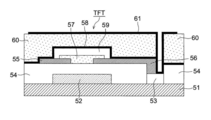
- FIG. 2 is a schematic cross-sectional view showing an example of the configuration of the organic thin film transistor of the present invention.
- the organic thin film transistor TFT includes a substrate 51, a gate electrode 52, a contact electrode 53, a source electrode 55, a drain electrode 56, and an organic semiconductor layer 57.
- a gate electrode 52 is provided on the substrate 51, and an insulating film 54 including a gate insulating film is provided so as to cover the gate electrode 52.
- a source electrode 55 and a drain electrode 56 are provided on the insulating film 54 so as to provide a space for forming a channel formed by the organic semiconductor layer 57.
- An organic semiconductor layer 57 is provided in a space between the source electrode 55 and the drain electrode 56 to connect them.
- 58 and 59 are passivation layers
- 60 is a photosensitive insulating film
- 61 is a pixel electrode.
- the substrate is not particularly limited, and for example, a resin sheet such as glass or a flexible plastic film can be used.
- the plastic film include polyethylene terephthalate (PET), polyethylene naphthalate (PEN), polyethersulfone (PES), polyetherimide, polyetheretherketone, polyphenylene sulfide, polyarylate, polyimide, and polycarbonate.
- PET polyethylene terephthalate
- PEN polyethylene naphthalate
- PES polyethersulfone
- polyetherimide polyetheretherketone
- polyphenylene sulfide polyarylate
- polyimide polycarbonate
- PC cellulose triacetate
- CAP cellulose acetate propionate
- the gate electrode and the contact electrode are not particularly limited as long as they are conductive materials, and metal materials that can ensure sufficient conductivity are preferable.
- metal materials that can ensure sufficient conductivity are preferable.
- Al, Cr, Ag, Mo, a material obtained by adding doping to these, and the like can be given.
- the gate electrode and the contact electrode it is necessary to first provide a conductive thin film on the substrate.
- the conductive pattern forming method of the present invention is preferably used.
- a known method such as vapor deposition or sputtering can be used by using the above-mentioned material as a raw material, and then a gate electrode is formed by using a known photolithography process (resist application, exposure, development) and an etching process. be able to.
- a fluid electrode material is used, and it can be formed by a printing method such as relief printing, intaglio printing, flat plate, screen printing, or an ink jet method.
- a dispersion of conductive fine particles for example, a paste in which conductive fine particles made of metal or the like are dispersed in a dispersion medium that is water, an organic solvent, or a mixture thereof, preferably using a dispersion stabilizer made of an organic material.
- electroconductive fine particle dispersions such as ink, are mentioned. Since the conductive thin film is formed on the organic semiconductor, it is particularly preferable to use the above-described dispersion liquid as a dispersion medium mainly composed of water.
- conductive fine metal materials include platinum, gold, silver, cobalt, nickel, chromium, copper, iron, tin, antimony, lead, tantalum, indium, palladium, tellurium, rhenium, iridium, aluminum, ruthenium. , Germanium, molybdenum, tungsten, zinc, and the like can be used.
- platinum, gold, silver, copper, cobalt, chromium, iridium, nickel, palladium, molybdenum, and tungsten having a work function of 4.5 eV or more are preferable.
- the conductive polymer examples include known conductive polymers whose conductivity has been improved by doping, such as conductive polyaniline, conductive pyrrole, conductive polythiophene, polyethylenedioxythiophene and polystyrene sulfonic acid complex (PEDOT / PSS) and the like are preferably used. Among them, those having low electrical resistance at the contact surface with the semiconductor layer are preferable.
- the source electrode, drain electrode, and pixel electrode can be provided in the same manner as the gate electrode described above.
- the material constituting the organic semiconductor layer is not particularly limited, and various condensed polycyclic aromatic compounds and conjugated compounds can be applied.
- condensed polycyclic aromatic compound examples include compounds such as anthracene, tetracene, pentacene, hexacene, heptacene, phthalocyanine, porphyrin, and derivatives thereof.
- conjugated compound examples include polythiophene and its oligomer, polypyrrole and its oligomer, polyaniline, polyphenylene and its oligomer, polyphenylene vinylene (PPV) and its oligomer, polyethylene vinylene and its oligomer, polyacetylene, polydiacetylene, tetrathiafulvalene compound, quinone Compounds, cyano compounds such as tetracyanoquinodimethane, fullerenes and derivatives or mixtures thereof.
- an oligomer having an average molecular weight of 5000 or less is a preferred compound as the organic semiconductor material constituting the organic semiconductor layer, and an thiophene that can be preferably used in the present invention is a preferred compound.
- An oligomer is mentioned.
- the thiophene oligomer preferably used in the present invention includes a thiophene oligomer having a partial structure in which at least two or more substituted thiophene ring repeating units and an unsubstituted thiophene ring repeating unit are continuous,
- the number of thiophene rings contained in the thiophene oligomer is 8 to 40.
- the number of thiophene rings is preferably in the range of 8-20.
- the organic semiconductor layer includes, for example, materials having functional groups such as acrylic acid, acetamide, dimethylamino group, cyano group, carboxyl group, nitro group, benzoquinone derivatives, tetracyanoethylene and tetracyanoquinodimethane, and the like.
- a material that serves as an acceptor for accepting electrons such as a derivative thereof, a material having a functional group such as an amino group, a triphenyl group, an alkyl group, a hydroxyl group, an alkoxy group, or a phenyl group, a substituted amine such as phenylenediamine, Including an anthracene, benzoanthracene, substituted benzoanthracenes, pyrene, substituted pyrene, carbazole and its derivatives, tetrathiafulvalene and its derivatives, etc., materials that serve as donors of electrons, so-called doping treatment May be.
- Doping means introducing an electron-donating molecule (acceptor) or an electron-donating molecule (donor) into the organic semiconductor thin film as a dopant. Therefore, the doped thin film is a thin film containing the above-mentioned condensed polycyclic aromatic compound and a dopant. A well-known thing can be employ
- the organic semiconductor can be formed by a known method, such as vacuum deposition, CVD (Chemical Vapor Deposition), laser deposition, electron beam deposition, spin coating, dip coating, bar coating method, die coating method, And spray coating method, screen printing, ink jet printing, blade coating and the like.
- CVD Chemical Vapor Deposition
- laser deposition electron beam deposition
- spin coating dip coating
- bar coating method bar coating method
- die coating method die coating method
- spray coating method screen printing, ink jet printing, blade coating and the like.
- the patterning of the organic semiconductor can include direct patterning such as mask evaporation in the case of vapor deposition, patterning by photolithography after film formation on the entire surface, and ink jet printing.
- the film thickness of the organic semiconductor is not particularly limited, but the characteristics of the obtained transistor are often greatly influenced by the film thickness of the organic semiconductor film, and the film thickness varies depending on the organic semiconductor material used. In general, it is preferably 1 ⁇ m or less, particularly 10 to 300 nm.
- the passivation layers 58 and 59 may be composed only of an organic layer or only an inorganic layer, but a preferable configuration is a laminated configuration of an organic layer and an inorganic layer.
- the organic layer is preferably made of a material that does not adversely affect the organic semiconductor 7.
- Preferable materials include homopolymers and copolymers composed of components such as polyvinyl alcohol, polyvinyl pyrrolidone, HEMA, acrylic acid and acrylamide.
- An aqueous solution containing the above-described materials can be formed by a coating method such as spray coating, spin coating, blade coating, or dip coating, or a patterning method such as printing or ink jet.
- the inorganic layer is made of inorganic oxide or inorganic nitride such as silicon dioxide, silicon nitride, aluminum oxide, tantalum oxide, titanium dioxide, etc., atmospheric pressure plasma method, vacuum deposition method, molecular beam epitaxial growth method, ion cluster beam method, low energy It can be formed by an ion beam method, an ion plating method, a CVD method, a sputtering method, a spray coating method, a spin coating method, a blade coating method, a coating method such as a dip coating method, or a patterning method such as printing or inkjet. .
- Example 1 [Preparation of substrate] (Preparation of substrate 1-1) After the corona discharge treatment was performed on the PET substrate, it was immersed in a 2% by mass ODS (octadecyltriethoxysilane) aqueous solution at room temperature for 10 minutes and dried at 120 ° C. for 30 minutes to obtain a substrate 1-1.
- ODS octadecyltriethoxysilane
- the film was applied by spin coating so as to have a thickness of 50 nm and baked at 450 ° C. to obtain a photomask 1-2 having a titanium dioxide layer.
- the film was applied by spin coating so that the dry film thickness was 50 nm and baked at 450 ° C. to obtain a photomask 1-3 having a titanium dioxide layer.
- a dispersion containing titanium dioxide having a primary particle diameter of 10 nm is applied to quartz glass by a spin coat method so that the dry film thickness is 50 nm, and baked at 450 ° C. to form a titanium dioxide layer.
- Sample preparation [Preparation of Sample 1-1] (Formation of conductive pattern)
- the surface treated with ODS of the substrate 1-1 and the Cr layer of the photomask 1-1 were brought into close contact, and exposed for 10 minutes using a high-pressure mercury lamp having a dominant wavelength of 365 nm.
- the obtained base material was immersed in a Pd catalyst solution and dried, and further immersed in an electroless copper plating solution and dried to obtain Sample 1-1.
- Sample 1-2 (Formation of conductive pattern)
- the surface treated with ODS of the substrate 1-1 and the Cr layer of the photomask 1-1 were brought into close contact, and exposed for 10 minutes using a low-pressure mercury lamp having a dominant wavelength of 254 nm.
- the obtained base material was immersed in a Pd catalyst solution and dried, and further immersed in an electroless copper plating solution and dried to obtain Sample 1-2.
- Sample 1-3 (Formation of conductive pattern) The distance between the surface of the substrate 1-1 treated with octadecyltriethoxysilane and the titanium dioxide layer of the photomask 1-2 was set to 50 nm, and exposure was performed for 10 minutes using a high-pressure mercury lamp having a dominant wavelength of 365 nm. The obtained base material was immersed in a Pd catalyst solution and dried, and further immersed in an electroless copper plating solution and dried to obtain Sample 1-3.
- Sample 1-4 (Formation of conductive pattern)
- the surface treated with the compound A-1 of the substrate 1-2 and the Cr layer of the photomask 1-1 were brought into close contact, and exposed for 10 minutes using a high-pressure mercury lamp having a dominant wavelength of 365 nm.
- the obtained base material was immersed in a Pd catalyst solution and dried, and further immersed in an electroless copper plating solution and dried to obtain Sample 1-4.
- Sample 1-5 (Formation of conductive pattern) The distance between the surface of the substrate 1-2 treated with the compound A-1 and the titanium dioxide layer of the photomask 1-2 was set to 50 nm, and exposure was performed for 10 minutes using a high-pressure mercury lamp having a dominant wavelength of 365 nm. The obtained base material was immersed in a Pd catalyst solution and dried, and further immersed in an electroless copper plating solution and dried to obtain Sample 1-5.
- Sample 1-6 (Formation of conductive pattern) The distance between the surface of the substrate 1-3 treated with the compound A-2 and the titanium dioxide layer of the photomask 1-2 was set to 50 nm, and exposure was performed for 10 minutes using a high-pressure mercury lamp having a dominant wavelength of 365 nm. The obtained base material was immersed in a Pd catalyst solution and dried, and further immersed in an electroless copper plating solution and dried to obtain Sample 1-6.
- Sample 1-7 (Formation of conductive pattern) The distance between the surface of the substrate 1-4 treated with the compound A-3 and the titanium dioxide layer of the photomask 1-2 was set to 50 nm, and exposure was performed for 10 minutes using a high-pressure mercury lamp having a dominant wavelength of 365 nm. The obtained base material was immersed in a Pd catalyst solution and dried, and further immersed in an electroless copper plating solution and dried to obtain Sample 1-7.
- Sample 1-8 (Formation of conductive pattern) The distance between the surface of the substrate 1-2 treated with the compound A-1 and the titanium dioxide layer of the photomask 1-3 was set to 50 nm, and exposure was performed for 10 minutes using a high-pressure mercury lamp having a dominant wavelength of 365 nm. The obtained base material was immersed in a Pd catalyst solution and dried, and further immersed in an electroless copper plating solution and dried to obtain Sample 1-8.
- Sample 1-9 (Formation of conductive pattern) The distance between the surface of the substrate 1-2 treated with the compound A-1 and the Cr layer of the photomask 1-4 was set to 50 nm, and exposure was performed for 10 minutes using a high-pressure mercury lamp having a dominant wavelength of 365 nm. The obtained base material was immersed in a Pd catalyst solution and dried, and further immersed in an electroless copper plating solution and dried to obtain Sample 1-9.
- Table 1 shows the composition of each sample obtained as described above.
- the surface of the sample was observed with a KEYENCE microscope VHX-600, and the fine line reproducibility was evaluated according to the following criteria.
- the width and line spacing are reproduced with an accuracy within ⁇ 20%.
- X The line width and line spacing reproduction accuracy is ⁇ . Table 1 shows the results of evaluation exceeding 50%.
- the substrate surface treated with the compound represented by the general formula (1) according to the present invention was exposed to light using a photomask having a titanium dioxide layer having a photocatalytic action, and was prepared by plating. It was found that the obtained sample of the present invention was superior in the adhesion between the substrate and the conductive pattern and high in fine line reproducibility compared with the comparative sample.
- Example 2 [Production of photomask] (Preparation of photomask 1-1) (Preparation of photomask 2-1) A photomask 2-1 was obtained in the same manner as the photomask 1-1 of Example 1 except that the pattern shape was that of a source electrode and a drain electrode.
- a photomask 2-2 was obtained in the same manner as the photomask 1-2 of Example 1 except that the pattern shape was that of a source electrode and a drain electrode.
- a photomask 2-3 was obtained in the same manner as the photomask 1-3 of Example 1 except that the pattern shape was that of a source electrode and a drain electrode.
- a photomask 2-4 was obtained in the same manner as the photomask 1-4 of Example 1 except that the pattern shape was that of a source electrode and a drain electrode.
- Sample preparation An aluminum-neodymium (AlNd) film, which is an aluminum-based alloy, was formed on a glass substrate with a thickness of 150 nm by a sputtering method.
- the AlNd film was subjected to a photolithography process and an etching process to form a gate electrode and a contact electrode.
- a SiO 2 film having a thickness of 300 nm was formed using a plasma CVD method to obtain a gate insulating film.
- the entire substrate was immersed in a 2 mass% ODS aqueous solution for 10 minutes at room temperature and dried at 120 ° C. for 30 minutes.
- the ODS-treated surface and the Cr layer of the photomask 2-1 were brought into close contact with each other and exposed for 10 minutes using a high-pressure mercury lamp having a dominant wavelength of 365 nm.
- the obtained base material was immersed in a Pd catalyst solution and dried, and further immersed in an electroless copper plating solution and dried to obtain a sample 2-1 on which a source electrode and a drain electrode were formed.
- the entire substrate was immersed in a 2 mass% ODS aqueous solution for 10 minutes at room temperature and dried at 120 ° C. for 30 minutes.
- the ODS-treated surface and the Cr layer of the photomask 2-1 were brought into close contact with each other and exposed for 10 minutes using a low-pressure mercury lamp having a dominant wavelength of 254 nm.
- the obtained base material was dipped in a Pd catalyst solution and dried, and further dipped in an electroless copper plating solution and dried to obtain a sample 2-2 on which a source electrode and a drain electrode were formed.
- AlNd aluminum-neodymium
- AlNd film which is an aluminum-based alloy
- the AlNd film was subjected to a photolithography process and an etching process to form a gate electrode and a contact electrode.
- SiO 2 film having a thickness of 300 nm was formed using a plasma CVD method to obtain a gate insulating film.
- the entire substrate was immersed in a 2 mass% ODS aqueous solution at room temperature for 10 minutes and dried at 120 ° C. for 30 minutes.
- the interval between the ODS-treated surface and the titanium dioxide layer of the photomask 2-2 was set to 50 nm, and exposure was performed for 10 minutes using a high-pressure mercury lamp having a dominant wavelength of 365 nm.
- the obtained base material was dipped in a Pd catalyst solution and dried, and further dipped in an electroless copper plating solution and dried to obtain a sample 2-3 on which a source electrode and a drain electrode were formed.
- AlNd aluminum-neodymium
- AlNd aluminum-neodymium
- the AlNd film was subjected to a photolithography process and an etching process to form a gate electrode and a contact electrode.
- a SiO 2 film having a thickness of 300 nm was formed using a plasma CVD method to obtain a gate insulating film.
- the entire substrate was immersed in 2% by mass of Compound A-1 aqueous solution for 10 minutes at room temperature and dried at 120 ° C. for 30 minutes.
- the surface treated with Compound A-1 and the Cr layer of the photomask 2-1 were brought into close contact with each other, and exposed for 10 minutes using a high-pressure mercury lamp having a dominant wavelength of 365 nm.
- the obtained base material was dipped in a Pd catalyst solution and dried, and further dipped in an electroless copper plating solution and dried to obtain Sample 2-4 on which a source electrode and a drain electrode were formed.
- the entire substrate was immersed in 2% by mass of Compound A-1 aqueous solution for 10 minutes at room temperature and dried at 120 ° C. for 30 minutes.
- the distance between the surface treated with Compound A-1 and the titanium dioxide layer of the photomask 2-2 was set to 50 nm, and exposure was performed for 10 minutes using a high-pressure mercury lamp having a dominant wavelength of 365 nm.
- the obtained base material was dipped in a Pd catalyst solution and dried, and further dipped in an electroless copper plating solution and dried to obtain Sample 2-5 in which a source electrode and a drain electrode were formed.
- the entire substrate was immersed in a 2% by mass of Compound A-2 aqueous solution for 10 minutes at room temperature and dried at 120 ° C. for 30 minutes.
- the distance between the surface treated with Compound A-2 and the titanium dioxide layer of the photomask 2-2 was set to 50 nm, and exposure was performed for 10 minutes using a high-pressure mercury lamp having a dominant wavelength of 365 nm.
- the obtained base material was dipped in a Pd catalyst solution and dried, and further dipped in an electroless copper plating solution and dried to obtain Sample 2-6 in which a source electrode and a drain electrode were formed.
- the entire substrate was immersed in 2% by mass of Compound A-3 aqueous solution at room temperature for 10 minutes and dried at 120 ° C. for 30 minutes.
- the space between the surface treated with Compound A-3 and the titanium dioxide layer of the photomask 2-2 was set to 50 nm, and exposure was performed for 10 minutes using a high-pressure mercury lamp having a dominant wavelength of 365 nm.
- the obtained base material was dipped in a Pd catalyst solution and dried, and further dipped in an electroless copper plating solution and dried to obtain Sample 2-7 on which a source electrode and a drain electrode were formed.
- the entire substrate was immersed in 2% by mass of Compound A-1 aqueous solution for 10 minutes at room temperature and dried at 120 ° C. for 30 minutes.
- the distance between the surface treated with Compound A-1 and the titanium dioxide layer of the photomask 2-3 was set to 50 nm, and exposure was performed for 10 minutes using a high-pressure mercury lamp having a dominant wavelength of 365 nm.
- the obtained base material was dipped in a Pd catalyst solution and dried, and further dipped in an electroless copper plating solution and dried to obtain Sample 2-7 on which a source electrode and a drain electrode were formed.
- the entire substrate was immersed in 2% by mass of Compound A-1 aqueous solution for 10 minutes at room temperature and dried at 120 ° C. for 30 minutes.
- the space between the surface treated with Compound A-1 and the Cr layer of the photomask 2-4 was set to 50 nm, and exposure was performed for 10 minutes using a high-pressure mercury lamp having a dominant wavelength of 365 nm.
- the obtained base material was immersed in a Pd catalyst solution and dried, and further immersed in an electroless copper plating solution and dried to obtain Sample 2-9 on which a source electrode and a drain electrode were formed.
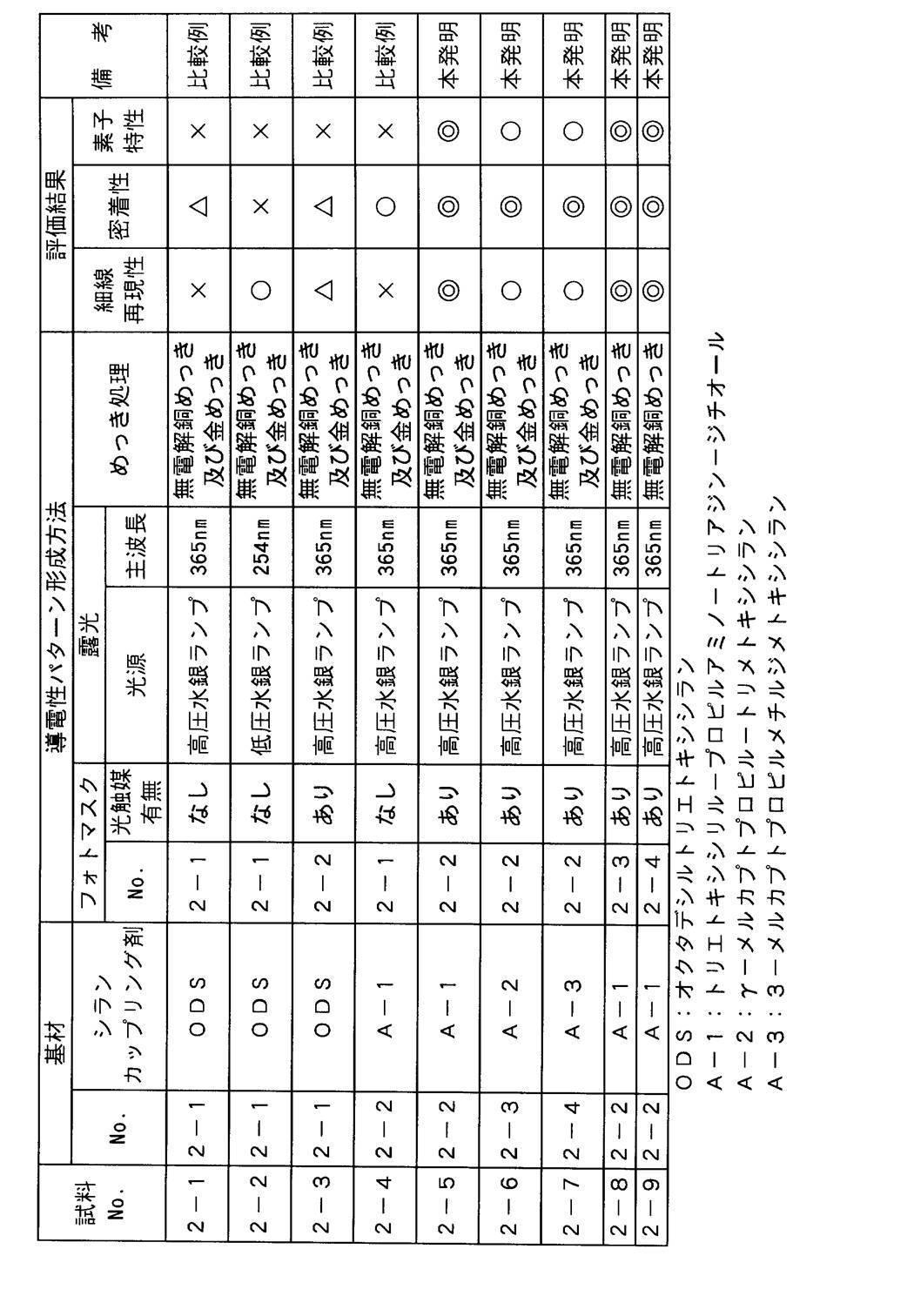
- Table 2 shows the composition of each sample obtained as described above.
- a 6,13-bistriisopropylsilylethynylpentacene (hereinafter referred to as pentacene) solution is dropped as an organic semiconductor material solution, and the organic semiconductor material solution is dropped approximately at the center of each source electrode and drain electrode of the sample using an inkjet method. Then, an organic semiconductor layer was formed so as to cover the drain electrode and the source electrode. At this time, the amount of the pentacene solution dropped was set to a dripping amount obtained in advance by experiments so that the thickness would be about 50 nm when the solvent was volatilized to form the organic semiconductor layer.
- PVA124C (trade name, Kuraray Co., Ltd .: non-photosensitive polyvinyl alcohol resin) is formed to a thickness of about 2 ⁇ m using a spin coating method, and unnecessary portions are removed by photolithography and etching, and passivation is performed. A layer was obtained.
- a passivation layer made of SiO 2 having a thickness of 50 nm was formed using an atmospheric pressure plasma method.
- PC403 (trade name, JSR Corporation) was applied to the passivation layer as a photosensitive insulating film with a thickness of 1 ⁇ m. Thereafter, a contact hole for connecting the drain electrode and a pixel electrode to be described later was formed by performing a photolithography process (exposure and development) using PC403 as a resist. Specifically, the PC403, which is a photosensitive insulating film in the contact hole portion, is removed by mask exposure and development processing, and then washed with water to remove the PVA124C, which is an exposed portion of the passivation film, thereby removing one of the drain electrodes. The part was exposed.
- ITO Indium Tin Oxide
- a contact electrode and a pixel electrode are formed by performing a photolithography process and an etching process.
- an organic thin film transistor was completed.
- the switching characteristics were evaluated according to the following criteria as an index of the element characteristics of the produced organic thin film transistor.
- ON / OFF ratio is 10 5 or more ⁇ : ON / OFF ratio is 10 3 or more, less than 10 5 ⁇ : ON / OFF ratio is less than 10 3 ⁇ : No operation Evaluation of adhesion, fine line reproducibility and element characteristics Table 2 shows the results.
Landscapes
- Chemical & Material Sciences (AREA)
- Engineering & Computer Science (AREA)
- Chemical Kinetics & Catalysis (AREA)
- General Chemical & Material Sciences (AREA)
- Materials Engineering (AREA)
- Mechanical Engineering (AREA)
- Metallurgy (AREA)
- Organic Chemistry (AREA)
- Physics & Mathematics (AREA)
- Health & Medical Sciences (AREA)
- General Physics & Mathematics (AREA)
- Toxicology (AREA)
- Manufacturing & Machinery (AREA)
- Optics & Photonics (AREA)
- Microelectronics & Electronic Packaging (AREA)
- Inorganic Chemistry (AREA)
- Spectroscopy & Molecular Physics (AREA)
- Electrodes Of Semiconductors (AREA)
- Internal Circuitry In Semiconductor Integrated Circuit Devices (AREA)
- Chemically Coating (AREA)
Abstract
Description
(式中、Rは炭素原子数8以下のアルキル基を、Aはアルコキシ基またはハロゲン原子を、BはSH基を含む置換基を表し、nは0~2の整数を表す。)
2.前記一般式(1)で表される化合物が、トリアジン環を有することを特徴とする前記1に記載の導電性パターン形成方法。
前記一般式(1)において、Rは炭素原子数8以下のアルキル基を表し、好ましくは炭素原子数1~4の低級アルキル基である。
A-2:γ-メルカプトプロピル-トリメトキシシラン
A-3:3-メルカプトプロピルメチルジメトキシシラン
A-4:メルカプトプロピルトリエトキシシラン
A-5:γ-メルカプトプロピルメチルジメトキシシラン
A-6:γ-メルカプトプロピル-トリクロルシラン
上記一般式(1)で表される化合物のうち、トリアジン環を有する化合物が特に好ましく、例えば、A-1は、γ-プロピルトリエトキシシランと対応するメルカプトアミン類、この場合1-アミノ-3,5-ジメルカプトトリアジン(特開2001-316872号等に記載)を縮合反応させることで容易に得られる。
本発明の導電性パターン形成方法は、前記一般式(1)で表される化合物で処理する工程と、光触媒作用により前記一般式(1)で表される化合物を分解する工程と、めっき工程を含むことを特徴とする。
本発明の導電性パターンの形成方法は、被形成部材に前記一般式(1)で表される化合物を含有する液を接触させて、一般式(1)で表される化合物をシロキサン結合を介して、前記被形成部材に結合させることを特徴とする。一般式(1)で表される化合物を含有する溶液の溶媒としては、水、水系溶媒、有機溶媒等、一般式(1)で表される化合物が溶解する溶媒であれば、いかなる溶媒種であってもよいが、ハンドリング性、乾燥性からアルコール系溶媒の使用が好ましく、さらに好ましくは、エタノール、イソプロパノールである。
次に、光触媒作用を有する化合物から成る層を有するフォトマスクを介して、主波長が300nm以上、400nm以下である光源で露光することで、光が照射された領域は光触媒作用で発生する活性酸素により、一般式(1)で表される化合物が分解され、光が照射されない領域は一般式(1)で表される化合物がそのまま残る。
一般式(1)で表される化合物は、金属との密着性が高いため、前記露光工程によって、金属が密着し易い領域と金属が密着し難い領域を作り出すことができる。前記露光工程の後にめっき処理を施して、光非照射領域に選択的にめっき膜を形成させることができる。導電性パターン形成に必要なフォトリソグラフ等の煩雑な処理を省略し、簡便かつ短時間で、導電性パターンを得ることができる。また、アンカー部は-O-Si基で結合されているので、良好な膜付き強度を有するめっき膜を得ることができる。
本発明で用いることのできる基板としては、例えば、ポリエチレンやポリプロピレン等のポリオレフィン類、ポリカーボネート類、セルロースアセテート、ポリエチレンテレフタレート、ポリエチレンジナフタレンジカルボキシラート、ポリエチレンナフタレート類、ポリ塩化ビニル、ポリイミド、ポリビニルアセタール類、ポリスチレン等の合成プラスチックフィルムも好ましく使用できる。また、シンジオタクチック構造ポリスチレン類も好ましい。これらは、例えば、特開昭62-117708号、特開平1-46912号、同1-178505号の各公報に記載されている方法により得ることができる。さらに、ステンレス等の金属製基盤や、バライタ紙、及びレジンコート紙等の紙支持体ならびに上記プラスチックフィルムに反射層を設けた支持体、特開昭62-253195号(29~31頁)に支持体として記載されたものが挙げられる。RDNo.17643の28頁、同No.18716の647頁右欄から648頁左欄及び同No.307105の879頁に記載されたものも好ましく使用できる。これらの支持体には、米国特許第4,141,735号のようにTg以下の熱処理を施すことで、巻き癖をつきにくくしたものを用いることができる。また、これらの支持体表面を支持体と他の構成層との接着の向上を目的に表面処理を行ってもよい。本発明では、グロー放電処理、紫外線照射処理、コロナ処理、火炎処理を表面処理として用いることができる。さらに公知技術第5号(1991年3月22日アズテック有限会社発行)の44~149頁に記載の支持体を用いることもできる。さらにRDNo.308119の1009頁やプロダクト・ライセシング・インデックス、第92巻P108の「Supports」の項に記載されているものが挙げられる。その他に、ガラス基板や、ガラスを練りこんだエポキシ樹脂を用いることができる。
本発明の導電性パターン形成方法は、有機薄膜トランジスタの作製に応用することができる。有機薄膜トランジスタの導電性パターンの例としては、画素電極、ソース電極、ドレイン電極、ゲート電極、コンタクト電極が挙げられる。本発明の導電性パターンの形成方法で形成される電極として好ましいのはソース電極、ドレイン電極である。
以下、本発明の有機薄膜トランジスタの各構成要素について、詳細な説明をする。
〔基材の作製〕
(基材1-1の作製)
PET基板にコロナ放電処理を行った後、2質量%のODS(オクタデシルトリエトキシシラン)水溶液に室温で10分間浸漬し、120℃で30分間乾燥させて基材1-1を得た。
PET基板にコロナ放電処理を行った後、2質量%の化合物A-1水溶液に室温で10分間浸漬し、120℃で30分間乾燥させて基材1-2を得た。
PET基板にコロナ放電処理を行った後、2質量%の化合物A-2水溶液に室温で10分間浸漬し、120℃で30分間乾燥させて基材1-3を得た。
PET基板にコロナ放電処理を行った後、2質量%の化合物A-3水溶液に室温で10分間浸漬し、120℃で30分間乾燥させて基材1-4を得た。
(フォトマスク1-1の作製)
石英ガラスにスパッタ法で50nmのCr層を形成し、フォトリソグラフ法でL/S=10μm/10μmのパターンを形成して、フォトマスク1-1を得た。
石英ガラスにスパッタ法で50nmのCr層を形成し、フォトリソグラフ法でL/S=10μm/10μmのパターンを形成し、次に一次粒径10nmの二酸化チタンを有する分散物をCr上に乾燥膜厚が50nmになるようにスピンコート法で塗布し、450℃で焼成して、二酸化チタン層を有するフォトマスク1-2を得た。
石英ガラスにスパッタ法で50nmのCr層を形成し、フォトリソグラフ法でL/S=10μm/10μmのパターンを形成し、次に一次粒径10nmの二酸化チタンを有する分散物を石英ガラス面上に乾燥膜厚が50nmになるようにスピンコート法で塗布し、450℃で焼成して、二酸化チタン層を有するフォトマスク1-3を得た。
石英ガラスに一次粒径10nmの二酸化チタンを有する分散物を石英ガラス面上に乾燥膜厚が50nmになるようにスピンコート法で塗布し、450℃で焼成して二酸化チタン層を形成し、次に二酸化チタン層上にスパッタ法で50nmのCr層を形成し、フォトリソグラフ法でCr層のみをエッチングして、L/S=10μm/10μmのパターンを形成し、二酸化チタン層を有するフォトマスク1-4を得た。
〔試料1-1の作製〕
(導電性パターンの形成)
基材1-1のODSで処理した面とフォトマスク1-1のCr層を密着させ、主波長が365nmである高圧水銀ランプを用いて10分間露光した。得られた基材をPd触媒溶液に浸漬後、乾燥し、さらに無電解銅メッキ液に浸漬後、乾燥させて、試料1-1を得た。
(導電性パターンの形成)
基材1-1のODSで処理した面とフォトマスク1-1のCr層を密着させ、主波長が254nmである低圧水銀ランプを用いて10分間露光した。得られた基材をPd触媒溶液に浸漬後、乾燥し、さらに無電解銅メッキ液に浸漬後、乾燥させて、試料1-2を得た。
(導電性パターンの形成)
基材1-1のオクタデシルトリエトキシシランで処理した面とフォトマスク1-2の二酸化チタン層の間隔を50nmに設定し、主波長が365nmである高圧水銀ランプを用いて10分間露光した。得られた基材をPd触媒溶液に浸漬後、乾燥し、さらに無電解銅メッキ液に浸漬後、乾燥させて、試料1-3を得た。
(導電性パターンの形成)
基材1-2の化合物A-1で処理した面とフォトマスク1-1のCr層を密着させ、主波長が365nmである高圧水銀ランプを用いて10分間露光した。得られた基材をPd触媒溶液に浸漬後、乾燥し、さらに無電解銅メッキ液に浸漬後、乾燥させて、試料1-4を得た。
(導電性パターンの形成)
基材1-2の化合物A-1で処理した面とフォトマスク1-2の二酸化チタン層の間隔を50nmに設定し、主波長が365nmである高圧水銀ランプを用いて10分間露光した。得られた基材をPd触媒溶液に浸漬後、乾燥し、さらに無電解銅メッキ液に浸漬後、乾燥させて、試料1-5を得た。
(導電性パターンの形成)
基材1-3の化合物A-2で処理した面とフォトマスク1-2の二酸化チタン層の間隔を50nmに設定し、主波長が365nmである高圧水銀ランプを用いて10分間露光した。得られた基材をPd触媒溶液に浸漬後、乾燥し、さらに無電解銅メッキ液に浸漬後、乾燥させて、試料1-6を得た。
(導電性パターンの形成)
基材1-4の化合物A-3で処理した面とフォトマスク1-2の二酸化チタン層の間隔を50nmに設定し、主波長が365nmである高圧水銀ランプを用いて10分間露光した。得られた基材をPd触媒溶液に浸漬後、乾燥し、さらに無電解銅メッキ液に浸漬後、乾燥させて、試料1-7を得た。
(導電性パターンの形成)
基材1-2の化合物A-1で処理した面とフォトマスク1-3の二酸化チタン層の間隔を50nmに設定し、主波長が365nmである高圧水銀ランプを用いて10分間露光した。得られた基材をPd触媒溶液に浸漬後、乾燥し、さらに無電解銅メッキ液に浸漬後、乾燥させて、試料1-8を得た。
(導電性パターンの形成)
基材1-2の化合物A-1で処理した面とフォトマスク1-4のCr層の間隔を50nmに設定し、主波長が365nmである高圧水銀ランプを用いて10分間露光した。得られた基材をPd触媒溶液に浸漬後、乾燥し、さらに無電解銅メッキ液に浸漬後、乾燥させて、試料1-9を得た。
(密着性の評価)
指の腹で試料表面にセロハンテープ(「CT24」ニチバン(株)製)を密着させた後にセロハンテープを一気に剥離して、剥離された導電性のパターンの面積比率を求め、下記の基準に従って、密着性を評価した。
○:導電性パターンの剥離面積が0%より大きく、1.0%以下
△:導電性パターンの剥離面積が1.0%より大きく、5.0%以下
×:導電性パターンの剥離面積が5.0%より大きい
(細線再現性の評価)
キーエンス社製マイクロスコープVHX-600で試料表面を観察して、下記の基準に従って、細線再現性を評価した
◎:線幅及び線の間隔が±10%以内の精度で再現されている
○:線幅及び線の間隔が±20%以内の精度で再現されている
△:線幅及び線の間隔が±50%以内の精度で再現されている
×:線幅及び線の間隔の再現精度が±50%を超える
評価の結果を表1に示す。

〔フォトマスクの作製〕
(フォトマスク1-1の作製)
(フォトマスク2-1の作製)
パターン形状がソース電極とドレイン電極の形状である以外は、実施例1のフォトマスク1-1と同様にしてフォトマスク2-1を得た。
パターン形状がソース電極とドレイン電極の形状である以外は、実施例1のフォトマスク1-2と同様にしてフォトマスク2-2を得た。
パターン形状がソース電極とドレイン電極の形状である以外は、実施例1のフォトマスク1-3と同様にして、フォトマスク2-3を得た。
パターン形状がソース電極とドレイン電極の形状である以外は、実施例1のフォトマスク1-4と同様にしてフォトマスク2-4を得た。
〔試料2-1の作製〕
ガラス基板に、アルミニウム系合金であるアルミニウム-ネオジム(AlNd)膜を厚み150nmとしてスパッタ法を用いて成膜した。このAlNd膜に対し、フォトリソグラフィー処理及びエッチング処理を行い、ゲート電極とコンタクト電極を形成した。次に、SiO2膜を厚み300nmとしてプラズマCVD法を用いて成膜して、ゲート絶縁膜を得た。
ガラス基板に、アルミニウム系合金であるアルミニウム-ネオジム(AlNd)膜を厚み150nmとしてスパッタ法を用いて成膜した。このAlNd膜に対し、フォトリソグラフィー処理及びエッチング処理を行い、ゲート電極とコンタクト電極を形成した。次に、SiO2膜を厚み300nmとしてプラズマCVD法を用いて成膜して、ゲート絶縁膜を得た。
ガラス基板にアルミニウム系合金であるアルミニウム-ネオジム(AlNd)膜を厚み150nmとしてスパッタ法を用いて成膜した。このAlNd膜に対し、フォトリソグラフィー処理及びエッチング処理を行い、ゲート電極とコンタクト電極を形成した。次に、SiO2膜を厚み300nmとしてプラズマCVD法を用いて成膜して、ゲート絶縁膜を得た。
ガラス基板にアルミニウム系合金であるアルミニウム-ネオジム(AlNd)膜を厚み150nmとしてスパッタ法を用いて成膜した。このAlNd膜に対し、フォトリソグラフィー処理及びエッチング処理を行い、ゲート電極とコンタクト電極を形成した。次に、SiO2膜を厚み300nmとしてプラズマCVD法を用いて成膜して、ゲート絶縁膜を得た。
ガラス基板1にアルミニウム系合金であるアルミニウム-ネオジム(AlNd)膜を厚み150nmとしてスパッタ法を用いて成膜した。このAlNd膜に対し、フォトリソグラフィー処理及びエッチング処理を行い、ゲート電極とコンタクト電極を形成した。次に、SiO2膜を厚み300nmとしてプラズマCVD法を用いて成膜して、ゲート絶縁膜4を得た。
ガラス基板にアルミニウム系合金であるアルミニウム-ネオジム(AlNd)膜を厚み150nmとしてスパッタ法を用いて成膜した。このAlNd膜に対し、フォトリソグラフィー処理及びエッチング処理を行い、ゲート電極とコンタクト電極を形成した。次に、SiO2膜を厚み300nmとしてプラズマCVD法を用いて成膜して、ゲート絶縁膜を得た。
ガラス基板にアルミニウム系合金であるアルミニウム-ネオジム(AlNd)膜を厚み150nmとしてスパッタ法を用いて成膜した。このAlNd膜に対し、フォトリソグラフィー処理及びエッチング処理を行い、ゲート電極とコンタクト電極を形成した。次に、SiO2膜を厚み300nmとしてプラズマCVD法を用いて成膜して、ゲート絶縁膜を得た。
ガラス基板にアルミニウム系合金であるアルミニウム-ネオジム(AlNd)膜を厚み150nmとしてスパッタ法を用いて成膜した。このAlNd膜に対し、フォトリソグラフィー処理及びエッチング処理を行い、ゲート電極とコンタクト電極を形成した。次に、SiO2膜を厚み300nmとしてプラズマCVD法を用いて成膜して、ゲート絶縁膜を得た。
ガラス基板にアルミニウム系合金であるアルミニウム-ネオジム(AlNd)膜を厚み150nmとしてスパッタ法を用いて成膜した。このAlNd膜に対し、フォトリソグラフィー処理及びエッチング処理を行い、ゲート電極とコンタクト電極を形成した。次に、SiO2膜を厚み300nmとしてプラズマCVD法を用いて成膜して、ゲート絶縁膜を得た。
(密着性及び細線再現性の評価)
実施例1と同様にして密着性及び細線再現性を評価した。
上記で作製した試料を用いて下記に記載の方法で有機薄膜トランジスタを作製した。
○:ON/OFF比が103以上、105未満
△:ON/OFF比が103未満
×:動作せず
密着性、細線再現性及び素子特性の評価の結果を表2に示す。
11、51 基板
12 基材
21 一般式(1)で表される化合物を含む層
22 一般式(1)で表される化合物が分解された領域
31 銅
40 フォトマスク
41 石英ガラス
42 二酸化チタン層
43 Cr層
52 ゲート電極
53 コンタクト電極
54 絶縁膜
55 ソース電極
56 ドレイン電極
57 有機半導体層
58、59 パッシベーション層
60 感光性絶縁膜
61 画素電極
Claims (9)
- 基板表面を下記一般式(1)で表される化合物で処理する工程と、光触媒作用により前記一般式(1)で表される化合物を分解する工程と、めっき工程を含むことを特徴とする導電性パターン形成方法。
一般式(1) (R)n-Si(A)3-n-(B)
(式中、Rは炭素原子数8以下のアルキル基を、Aはアルコキシ基またはハロゲン原子を、BはSH基を含む置換基を表し、nは0~2の整数を表す。) - 前記一般式(1)で表される化合物が、トリアジン環を有することを特徴とする請求項1に記載の導電性パターン形成方法。
- 前記光触媒作用が二酸化チタンの光触媒作用であることを特徴とする請求項1または2に記載の導電性パターン形成方法。
- 前記一般式(1)で表される化合物を分解する工程が、二酸化チタン膜を有するフォトマスクを用いた露光工程であることを特徴とする請求項3に記載の導電性パターン形成方法。
- 前記露光工程の光源の主波長が300nm以上、400nm以下であることを特徴とする請求項4に記載の導電性パターン形成方法。
- 前記光源に高圧水銀ランプを用いることを特徴とする請求項5に記載の導電性パターン形成方法。
- 前期めっき処理工程が触媒担持工程と無電解めっき処理工程を有することを特徴とする請求項1~6のいずれか1項に記載の導電性パターン形成方法。
- 請求項1~7のいずれか1項に記載の導電性パターン形成方法を用いて導電性パターンが形成されていることを特徴とする有機薄膜トランジスタ。
- 前記導電性パターンがソース電極またはドレイン電極であることを特徴とする請求項8に記載の有機薄膜トランジスタ。
Priority Applications (2)
| Application Number | Priority Date | Filing Date | Title |
|---|---|---|---|
| JP2010521659A JPWO2010010792A1 (ja) | 2008-07-24 | 2009-06-29 | 導電性パターン形成方法及び有機薄膜トランジスタ |
| US13/054,913 US20110133192A1 (en) | 2008-07-24 | 2009-06-29 | Method of forming conductive pattern and organic thin film transistor |
Applications Claiming Priority (2)
| Application Number | Priority Date | Filing Date | Title |
|---|---|---|---|
| JP2008190798 | 2008-07-24 | ||
| JP2008-190798 | 2008-07-24 |
Publications (1)
| Publication Number | Publication Date |
|---|---|
| WO2010010792A1 true WO2010010792A1 (ja) | 2010-01-28 |
Family
ID=41570258
Family Applications (1)
| Application Number | Title | Priority Date | Filing Date |
|---|---|---|---|
| PCT/JP2009/061840 Ceased WO2010010792A1 (ja) | 2008-07-24 | 2009-06-29 | 導電性パターン形成方法及び有機薄膜トランジスタ |
Country Status (3)
| Country | Link |
|---|---|
| US (1) | US20110133192A1 (ja) |
| JP (1) | JPWO2010010792A1 (ja) |
| WO (1) | WO2010010792A1 (ja) |
Cited By (2)
| Publication number | Priority date | Publication date | Assignee | Title |
|---|---|---|---|---|
| JP2015089951A (ja) * | 2013-11-05 | 2015-05-11 | キヤノン・コンポーネンツ株式会社 | 金属皮膜付物品及びその製造方法並びに配線板 |
| JP2016108615A (ja) * | 2014-12-05 | 2016-06-20 | アキレス株式会社 | パターン性が良好なめっき品の製造方法 |
Families Citing this family (1)
| Publication number | Priority date | Publication date | Assignee | Title |
|---|---|---|---|---|
| JP2019057572A (ja) * | 2017-09-20 | 2019-04-11 | 東芝メモリ株式会社 | 金属配線の形成方法 |
Citations (4)
| Publication number | Priority date | Publication date | Assignee | Title |
|---|---|---|---|---|
| JP2005072188A (ja) * | 2003-08-22 | 2005-03-17 | Univ Of Tokyo | 有機トランジスタの製造方法、及び有機トランジスタ |
| JP2007027312A (ja) * | 2005-07-14 | 2007-02-01 | Fujifilm Holdings Corp | 配線基板の製造方法および配線基板 |
| JP2008004586A (ja) * | 2006-06-20 | 2008-01-10 | Mitsubishi Plastics Ind Ltd | 導電回路パターンの形成方法 |
| JP2008047874A (ja) * | 2006-08-17 | 2008-02-28 | Samsung Electronics Co Ltd | 新規の金属パターンの製造方法及びこれを用いた平板表示素子 |
Family Cites Families (7)
| Publication number | Priority date | Publication date | Assignee | Title |
|---|---|---|---|---|
| JPS614761A (ja) * | 1984-06-18 | 1986-01-10 | Nippon Paint Co Ltd | 架橋反応プロモ−タ−微小樹脂粒子およびその使用方法 |
| DE69841945D1 (de) * | 1997-08-08 | 2010-11-25 | Dainippon Printing Co Ltd | Struktur zur Musterbildung, Verfahren zur Musterbildung und deren Anwendung |
| JP3384544B2 (ja) * | 1997-08-08 | 2003-03-10 | 大日本印刷株式会社 | パターン形成体およびパターン形成方法 |
| JP4635410B2 (ja) * | 2002-07-02 | 2011-02-23 | ソニー株式会社 | 半導体装置及びその製造方法 |
| JP2007063675A (ja) * | 2005-07-08 | 2007-03-15 | Daikin Ind Ltd | 有機溶媒存在下での表面処理 |
| JP2008153259A (ja) * | 2006-12-14 | 2008-07-03 | Konica Minolta Holdings Inc | 有機薄膜トランジスタ及び有機薄膜トランジスタの製造方法 |
| JP5092391B2 (ja) * | 2006-12-22 | 2012-12-05 | 富士通株式会社 | 樹脂筐体及びその製造方法 |
-
2009
- 2009-06-29 US US13/054,913 patent/US20110133192A1/en not_active Abandoned
- 2009-06-29 JP JP2010521659A patent/JPWO2010010792A1/ja active Pending
- 2009-06-29 WO PCT/JP2009/061840 patent/WO2010010792A1/ja not_active Ceased
Patent Citations (4)
| Publication number | Priority date | Publication date | Assignee | Title |
|---|---|---|---|---|
| JP2005072188A (ja) * | 2003-08-22 | 2005-03-17 | Univ Of Tokyo | 有機トランジスタの製造方法、及び有機トランジスタ |
| JP2007027312A (ja) * | 2005-07-14 | 2007-02-01 | Fujifilm Holdings Corp | 配線基板の製造方法および配線基板 |
| JP2008004586A (ja) * | 2006-06-20 | 2008-01-10 | Mitsubishi Plastics Ind Ltd | 導電回路パターンの形成方法 |
| JP2008047874A (ja) * | 2006-08-17 | 2008-02-28 | Samsung Electronics Co Ltd | 新規の金属パターンの製造方法及びこれを用いた平板表示素子 |
Cited By (2)
| Publication number | Priority date | Publication date | Assignee | Title |
|---|---|---|---|---|
| JP2015089951A (ja) * | 2013-11-05 | 2015-05-11 | キヤノン・コンポーネンツ株式会社 | 金属皮膜付物品及びその製造方法並びに配線板 |
| JP2016108615A (ja) * | 2014-12-05 | 2016-06-20 | アキレス株式会社 | パターン性が良好なめっき品の製造方法 |
Also Published As
| Publication number | Publication date |
|---|---|
| US20110133192A1 (en) | 2011-06-09 |
| JPWO2010010792A1 (ja) | 2012-01-05 |
Similar Documents
| Publication | Publication Date | Title |
|---|---|---|
| Kim et al. | Universal three-dimensional crosslinker for all-photopatterned electronics | |
| TWI401744B (zh) | 製備低電阻金屬導線之方法及其相關圖案化金屬導線結構與顯示裝置 | |
| JP4407311B2 (ja) | 薄膜トランジスタの製造方法 | |
| EP2001063A1 (en) | Organic semiconductor thin film, organic thin film transistor and method for manufacturing same | |
| Tsuruoka et al. | Laser patterning of optically reconfigurable transistor channels in a photochromic diarylethene layer | |
| US20110297938A1 (en) | Thin film transistor, method of manufacturing the same, and electronic device | |
| CN104641471A (zh) | 用于氧化物薄膜晶体管的涂层材料 | |
| CN102867914A (zh) | 电子器件和半导体器件的制造方法 | |
| Choi et al. | Monolithic metal oxide transistors | |
| JP2013070081A (ja) | スイッチング素子及びその製造方法 | |
| CN103733319A (zh) | 晶体管的制造方法及晶体管 | |
| WO2010010792A1 (ja) | 導電性パターン形成方法及び有機薄膜トランジスタ | |
| US11345778B2 (en) | Organic dielectric materials and devices including them | |
| JP5913108B2 (ja) | 有機半導体材料及び電界効果トランジスタ並びにその製造方法 | |
| GB2443577A (en) | Method for manufacturing thin film transistors | |
| CN104409635B (zh) | 一种有机薄膜晶体管及其制作方法、阵列基板、显示装置 | |
| Hong et al. | Photopatternable poly (4-styrene sulfonic acid)-wrapped MWNT thin-film source/drain electrodes for use in organic field-effect transistors | |
| US10741767B2 (en) | Organic thin film transistor, and fabricating method thereof | |
| TW202111976A (zh) | 有機半導體器件之源極/汲極用電極、使用其之有機半導體器件、及其等之製造方法 | |
| JP5729540B2 (ja) | 電界効果型トランジスタ及びその製造方法 | |
| JPWO2008018271A1 (ja) | 有機薄膜トランジスタとその製造方法 | |
| US20110121280A1 (en) | Substrate, conductive pattern formation process and organic thin film transistor | |
| JP2007019121A (ja) | 有機半導体装置製造用基板、有機半導体装置およびその製造方法 | |
| JP5055844B2 (ja) | 有機薄膜トランジスタ及び有機薄膜トランジスタの製造方法 | |
| JP2008053607A (ja) | カーボンナノチューブ分散ポリマーを用いた電界効果トランジスタの製造方法 |
Legal Events
| Date | Code | Title | Description |
|---|---|---|---|
| 121 | Ep: the epo has been informed by wipo that ep was designated in this application |
Ref document number: 09800307 Country of ref document: EP Kind code of ref document: A1 |
|
| WWE | Wipo information: entry into national phase |
Ref document number: 2010521659 Country of ref document: JP |
|
| WWE | Wipo information: entry into national phase |
Ref document number: 13054913 Country of ref document: US |
|
| NENP | Non-entry into the national phase |
Ref country code: DE |
|
| 122 | Ep: pct application non-entry in european phase |
Ref document number: 09800307 Country of ref document: EP Kind code of ref document: A1 |