WO2009148010A1 - 光導波路の製造方法およびそれに用いる型 - Google Patents
光導波路の製造方法およびそれに用いる型 Download PDFInfo
- Publication number
- WO2009148010A1 WO2009148010A1 PCT/JP2009/059956 JP2009059956W WO2009148010A1 WO 2009148010 A1 WO2009148010 A1 WO 2009148010A1 JP 2009059956 W JP2009059956 W JP 2009059956W WO 2009148010 A1 WO2009148010 A1 WO 2009148010A1
- Authority
- WO
- WIPO (PCT)
- Prior art keywords
- core
- groove
- mold
- spacer
- substrate
- Prior art date
- Legal status (The legal status is an assumption and is not a legal conclusion. Google has not performed a legal analysis and makes no representation as to the accuracy of the status listed.)
- Ceased
Links
Images
Classifications
-
- G—PHYSICS
- G02—OPTICS
- G02B—OPTICAL ELEMENTS, SYSTEMS OR APPARATUS
- G02B6/00—Light guides; Structural details of arrangements comprising light guides and other optical elements, e.g. couplings
- G02B6/10—Light guides; Structural details of arrangements comprising light guides and other optical elements, e.g. couplings of the optical waveguide type
- G02B6/12—Light guides; Structural details of arrangements comprising light guides and other optical elements, e.g. couplings of the optical waveguide type of the integrated circuit kind
- G02B6/13—Integrated optical circuits characterised by the manufacturing method
- G02B6/138—Integrated optical circuits characterised by the manufacturing method by using polymerisation
-
- G—PHYSICS
- G02—OPTICS
- G02B—OPTICAL ELEMENTS, SYSTEMS OR APPARATUS
- G02B1/00—Optical elements characterised by the material of which they are made; Optical coatings for optical elements
- G02B1/04—Optical elements characterised by the material of which they are made; Optical coatings for optical elements made of organic materials, e.g. plastics
- G02B1/045—Light guides
Definitions
- the present invention relates to a method for manufacturing an optical waveguide and a mold used therefor.
- An optical waveguide typically has a buried structure in which a core layer having a high refractive index is surrounded by a cladding layer having a low refractive index, or a core having a high refractive index on a lower cladding layer having a low refractive index.
- a clad material is applied on a substrate and cured to form a lower clad layer, then a core material is applied onto the lower clad layer, and a mask is applied and cured.
- the core layer is formed by removing the uncured portion, or the core material is applied on the lower cladding layer and then cured, and then the patterned resist layer is formed, and the uncovered portion is removed.
- a method has been adopted in which a clad material is applied on the lower clad layer so as to embed the core layer and cured to form the upper clad layer.
- a stamper method has recently been studied as a method for manufacturing an optical waveguide simply and inexpensively.
- a clad material is dropped on a glass substrate, a stamper mold having a pattern having the same shape as the core layer is pressed on the surface to form a core groove, and then the clad material is cured.
- a method is disclosed in which a cladding material is dropped on a layer, a base substrate is adhered, and then the cladding material is cured to form an upper cladding layer.
- the conventional stamper method uses a glass substrate, it is limited to a single wafer process for manufacturing optical waveguides one by one, and the efficiency of manufacturing the optical waveguide is poor. Therefore, in order to improve the efficiency of manufacturing the optical waveguide, a roll of the film substrate is prepared, and the lower clad layer, the core layer, and the upper clad layer are sequentially formed on the film substrate while the film substrate is pulled out from the roll. Therefore, it is required to employ a continuous process for continuously manufacturing the optical waveguide.
- an opto-electric hybrid module is manufactured from an optical waveguide, light passes through the substrate. Therefore, considering the light transmission efficiency, the thickness is smaller than that of the glass substrate. It is preferable to use a film substrate that is short, has a refractive index close to that of the optical waveguide film, and therefore has little light reflection.
- JP 2006-227655 A Japanese Patent No. 3858899 Japanese Patent No. 3858995
- the film substrate has lower rigidity than the glass substrate, when the clad material is dropped on the film substrate and a stamper mold having the same shape pattern as the core layer is pressed on the surface, the film substrate is bent, There is a problem in that a lower clad layer having a substantially uniform thickness at a portion located below the core layer cannot be formed.
- the stamper mold is made of a flexible material, if the stamper mold is pressed against the surface of the substrate on which the clad material is dropped, the stamper mold is bent and the lower clad has a uniform thickness. If the rigidity of the substrate, clad material or stamper type is low, it is difficult to form a uniform thickness of the lower clad layer, and the optical waveguide has a small waveguide loss. There was a problem that it was difficult to obtain.
- An object of the present invention is to provide an optical waveguide manufacturing method capable of easily controlling the thickness of a lower clad layer at a position and a mold used therefor.
- the present inventors have responded not to a convex shape having only a convex portion corresponding to the core groove, but to a core groove and a spacer groove provided substantially parallel to each other on both sides of the core groove. If a lower cladding layer having a core groove and a spacer groove arranged substantially in parallel with a gap on both sides of the core groove is formed on the substrate using a convex mold having each convex portion, it corresponds to the spacer groove.
- the substrate or convex mold is supported and held substantially parallel without being bent, so that the thickness of the lower clad layer at the lower portion of the core layer can be easily made.
- the present invention has been completed by finding that it can be controlled.
- the present invention uses a second mold having a plurality of convex portions corresponding to a core groove and spacer grooves provided on both sides of the core groove with a space therebetween on the substrate. And forming a lower clad layer having spacer grooves disposed substantially parallel to each other on both sides of the core groove; injecting and filling the core material into the core groove, and curing the core material Forming a core layer; injecting and filling a clad material into the spacer groove, and applying the clad material on the lower clad layer so as to embed the core layer, and then curing the clad material And a step of forming an upper clad layer.
- the step of forming the lower clad layer includes dropping each of the clad material on the substrate, and having each convex portion corresponding to the core groove and spacer grooves that are provided substantially parallel to each other at both sides of the core groove. After placing the second mold, the clad material was cured, the second mold was removed, and the core groove and the core groove were provided substantially parallel to each other with a gap on both sides of the core groove. A step of forming a lower cladding layer having a spacer groove is preferable.
- the substrate is preferably a film substrate, and a ratio (y) of a depth (y) of the spacer groove to a distance (x) between the core groove and the spacer groove (y) / X) is preferably 1/10 or more and 3/1 or less. Further, after dropping the clad material on the substrate and placing the second mold, the second mold is pressed onto the substrate, and a convex portion corresponding to the spacer groove is formed on the substrate. It is preferable that the clad material is cured after being adhered.
- the cladding material and / or the core material is preferably a UV curable epoxy resin.
- the present invention is a mold used in the above-described method for manufacturing an optical waveguide, wherein each recess corresponding to a core groove and a spacer groove provided substantially parallel with a gap on both sides of the core groove.
- a mold characterized by having each convex part is provided.
- the depth (y) of the recess corresponding to the spacer groove with respect to the distance (x) between the recess corresponding to the core groove and the recess corresponding to the spacer groove ) Ratio (y / x), or the height (y) of the convex portion corresponding to the spacer groove with respect to the interval (x) between the convex portion corresponding to the core groove and the convex portion corresponding to the spacer groove.
- the ratio (y / x) is preferably 1/10 or more and 3/1 or less.
- An optical waveguide manufacturing method uses a second mold (convex mold) having respective convex portions corresponding to a core groove and spacer grooves arranged substantially parallel to each other on both sides of the core groove. Since the lower clad layer having a core groove and a spacer groove provided in parallel with a gap on both sides of the core groove is formed on the substrate, even if a low rigidity substrate such as a film substrate is used, Even when a clad material made of a material with low rigidity or a mold having a convex portion corresponding to the core groove is used, the lower clad layer located under the core layer has a substantially uniform thickness. In addition, an optical waveguide having a very small waveguide loss can be easily manufactured.
- the lower clad layer is formed by contacting the roll to which the second mold is attached, and then the core layer and the upper clad layer are sequentially formed.
- the obtained optical waveguide has a lower clad layer, a core layer, and an upper clad layer formed on a film substrate, if a film substrate with electrical wiring is used as the substrate, a light emitting element and / or a light receiving element By cutting the portion to mount V-shaped with a dicing saw to form a 45 ° mirror, the opto-electric hybrid module can be easily manufactured.
- An optical waveguide manufacturing method according to the present invention (hereinafter also referred to as “the manufacturing method of the present invention”) is substantially parallel by dropping a clad material on a substrate and spacing between the core groove and both sides of the core groove. After placing the second mold having the respective convex portions corresponding to the spacer grooves provided on the substrate, or on the substrate, the core grooves are provided substantially parallel to each other at intervals on both sides of the core groove.
- a second mold having respective convex portions corresponding to the spacer grooves is placed, and a clad material is injected and filled in a gap between the substrate and the second mold, and then the clad material is cured, Removing the second mold and forming, on the substrate, a lower clad layer having a core groove and spacer grooves arranged substantially parallel to each other on both sides of the core groove; Injecting and filling a core material and curing the core material to form a core layer; Injecting and filling a cladding material into the pacer groove and applying the cladding material on the lower cladding layer so as to embed the core layer, and then curing the cladding material to form an upper cladding layer; It is characterized by including.
- the manufacturing method of the present invention uses a soft lithography, and a second mold (convex mold) having convex portions corresponding to a core groove and spacer grooves that are provided in parallel with a gap on both sides of the core groove. ) Is used to form a lower clad layer on the substrate having a core groove and spacer grooves provided on both sides of the core groove so as to be substantially parallel to each other.
- Soft lithography is a kind of stamper method, and is a method of transferring a lower clad layer using a second mold (convex mold) formed of a soft material such as silicone rubber or urethane rubber. .
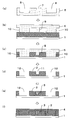
- a metal or an alloy such as phosphor bronze is cut, and a recess 7 corresponding to the core groove, a spacer groove that is provided in parallel with a gap on both sides of the core groove.
- the first mold (concave mold) 5 is manufactured by forming the concave section 8 corresponding to the above.
- a curable silicone material such as a two-component curable polysiloxane is applied to the first mold 5 and cured, and then the first mold 5 is removed, and FIG. As shown, a second mold (convex mold) having a convex section 9 corresponding to the core groove and a convex section (spacer) 10 corresponding to the spacer groove provided on both sides of the core groove with a space therebetween. 6 is produced.
- a release agent is applied on the first mold 5 so that the second mold 6 can be easily released from the first mold 5. Also good.
- a known release agent may be used as the release agent, and is not particularly limited.
- the projection corresponding to the spacer groove is formed on a stage having parallelism, for example.
- the second mold 6 is moved closer so that the portion (spacer) 10 contacts the substrate 1.
- the second mold 6 is temporarily stopped, and the defoaming process is performed by drawing a vacuum. It is preferred to remove bubbles from the cladding material.
- the clad is formed in the gap between the substrate 1 and the second mold 6.
- Material may be injected and filled.
- any known material can be used regardless of an inorganic material or an organic material.
- a silicon substrate a glass substrate such as quartz or pyrex (registered trademark); a metal such as Al or Cu. It is preferable to use a substrate; a metal oxide substrate; a resin substrate such as polyimide or polyetherketone; an organic-inorganic hybrid substrate.
- a resin substrate is preferable, and a film substrate made of a resin film is more preferable.
- the film substrate is not particularly limited as long as it is a resin film composed of a conventionally known optical waveguide material.
- a resin film composed of a conventionally known optical waveguide material.
- an epoxy resin, a polyimide resin, an acrylic resin, and a polyester resin are used.
- the resin film include resin, polystyrene resin, cycloolefin resin, polyethersulfone resin, polyetherketone resin, polyethernitrile resin, oxetane resin, silane resin, and silicone resin. .
- these resin films considering the production of the opto-electric hybrid module, from the viewpoint of heat resistance (particularly heat resistance assuming soldering, specifically 200-250 ° C.
- a polyimide resin That is, a film composed of a polyimide film (including a halogenated polyimide film) is preferable. Moreover, when using a polyimide film as a film substrate, you may utilize a commercial item. As a commercial item of a polyimide film, the brand name "Kapton (trademark)" series of Toray DuPont Co., Ltd. is mentioned, for example.
- the thickness of the substrate 1 may be appropriately selected according to the use of the optical waveguide or the wavelength of light used when the opto-electric hybrid module is manufactured, and is not particularly limited, but preferably 5 ⁇ m. More preferably, it is 10 ⁇ m or more, preferably 100 ⁇ m or less, more preferably 50 ⁇ m or less. If the thickness of the substrate 1 is too small, the strength of the substrate may decrease. On the other hand, if the thickness of the substrate 1 is too large, the transparency of the substrate may decrease when an opto-electric hybrid module is manufactured.
- the second die 6 in addition to the convex portion 9 corresponding to the core groove, the second die 6 has a convex portion (spacer) corresponding to a spacer groove provided in parallel with a gap on both sides of the core groove. 10 is provided, the substrate 1 or the second mold 6 bends when the second mold 6 is placed on the substrate 1 even if a low rigidity substrate such as a film substrate is used. There is not, and the space
- the thickness of the lower clad layer 2 at the lower portion of the core layer can be easily set. Can be controlled.
- the clad material constituting the lower clad layer 2 is not particularly limited as long as it is a conventionally known optical waveguide material.
- the clad material such as an ultraviolet (or light) curable resin or a thermosetting resin is used. Examples include resins and thermoplastic resins. Of these resins, ultraviolet (or light) curable resins are preferred.
- the ratio (y / x) of the depth (y) of the spacer groove 12 to the distance (x) between the core groove 11 and the spacer groove 12 is preferably 1/10 or more, more preferably 1 / It is 8 or more, more preferably 1/7 or more, preferably 3/1 or less, more preferably 2/1 or less, and further preferably 3/2 or less. If the ratio (y / x) is too small, the gap between the core groove 11 and the spacer groove 12 is too wide to form a sufficiently thick core layer, so that the lower cladding layer 2 is not formed on both sides of the core layer. More parts are needed and manufacturing costs may increase.
- the distance between the convex portion 9 corresponding to the core groove 11 and the convex portion 10 corresponding to the spacer groove 12 becomes large, and when the second die 6 is placed on the substrate 1. Since the second mold 6 is easily bent, the thickness of the lower clad layer 2 located on the lower side of the core layer may not be substantially uniform. Conversely, if the ratio (y / x) is too large, a sufficiently thick core layer can be formed, but the thickness of the lower cladding layer 2 in the portion located below the core layer becomes large, Again, manufacturing costs may increase.
- the depth of the spacer groove 12 is set to be substantially equal to the thickness of the lower cladding layer 2.
- the width of the spacer groove 12 may be appropriately adjusted according to the thickness of the lower cladding layer 2 and the like, and is not particularly limited. However, when the depth of the spacer groove 12 is 1, The number is preferably 2 or more, more preferably 5 or more, still more preferably 10 or more, and is preferably 50 or less, more preferably 30 or less, and still more preferably 20 or less. If the width of the spacer groove 12 is too small with respect to the depth of the spacer groove 12, the width of the convex portion (spacer) 10 corresponding to the spacer groove 12 in the second mold 6 becomes small.
- the substrate 1 or the second mold 6 may bend.
- the width of the spacer groove 12 is too large with respect to the depth of the spacer groove 12, the width of the convex portion (spacer) 10 corresponding to the spacer groove 12 in the second mold 6 becomes large.
- the material that constitutes the mold 6 and the cladding material that is injected and filled in the spacer grooves 12 of the lower cladding layer 2 are unnecessarily increased, which may increase the manufacturing cost.
- the thickness of the lower clad layer 2 may be appropriately selected according to the use of the optical waveguide, the wavelength of light to be used, and the like, and is not particularly limited, but preferably excluding the lower side of the core groove 11. It is 10 ⁇ m or more, more preferably 20 ⁇ m or more, and preferably 150 ⁇ m or less, more preferably 100 ⁇ m or less. If the thickness of the lower cladding layer 2 is too small, the core layer 3 having a sufficient thickness may not be formed. Conversely, if the thickness of the lower clad layer 2 is too large, the transparency of the lower clad layer 2 may be lowered when an opto-electric hybrid module is manufactured.
- the refractive index of the lower cladding layer 2 is not particularly limited as long as it is lower than the refractive index of the core layer 3.
- the type and composition of the cladding material are selected within the range of 1.45 to 1.65. By doing so, it can be arbitrarily adjusted.
- the second mold 6 is formed of silicone rubber and the lower cladding layer 2 is formed of a thermosetting resin, a thermoplastic resin, or an ultraviolet (or light) curable resin
- the second mold 6 is used.
- the lower clad layer 2 is formed several tens of times using 6, the second mold 6 may be deteriorated due to heat, change with time, or the like. Further, after the lower cladding layer 2 is formed, it may be contaminated by the residue of the cladding material. In such a case, the first mold 5 to the second mold 6 may be produced again and used.
- the core material is injected and filled into the core groove 11, and this core material is cured to form the core layer 3.
- the core layer 3 is formed in a straight line extending in a direction perpendicular to the paper surface, but may be formed in a predetermined pattern according to the use of the optical waveguide.
- the core material constituting the core layer 3 may be any conventionally known optical waveguide material as long as the refractive index is higher than that of the clad material constituting the lower clad layer 2 and the clad material constituting the upper clad layer 4, and is not particularly limited.
- a curable resin such as an ultraviolet (or light) curable resin or a thermosetting resin may be used. Of these resins, ultraviolet (or light) curable resins are preferred.
- the thickness of the core layer 3 may be appropriately selected according to the use of the optical waveguide or the wavelength of light to be used, and is not particularly limited, but is preferably 5 ⁇ m or more, more preferably 10 ⁇ m or more, Moreover, it is preferably 100 ⁇ m or less, more preferably 50 ⁇ m or less. If the thickness of the core layer 3 is too small, the amount of light propagating through the core layer 3 may decrease. Conversely, if the thickness of the core layer 3 is too large, the thickness of the lower cladding layer 2 is increased. In other words, unnecessary portions of the lower clad layer 2 increase on both sides of the core layer 3 and the manufacturing cost may increase. Moreover, since the thickness of the lower clad layer 2 and the core layer 3 constituting the optical waveguide is increased, the thickness of the optical waveguide film formed on the substrate 1 may be increased.
- the core layer 3 preferably has a rectangular cross-sectional shape perpendicular to the longitudinal direction, and most preferably has a square shape. That is, the aspect ratio (width / thickness) of the core layer 3 is preferably 1 ⁇ 2 or more, more preferably 2/3 or more, still more preferably 5/6 or more, and preferably 2/1 or less. More preferably, it is 3/2 or less, more preferably 6/5 or less. Most preferably, it is 1/1. If the aspect ratio of the core layer 3 is too small or too large, the cross-sectional shape perpendicular to the longitudinal direction of the core layer 3 becomes flat, so that light enters the core layer 3 or the core layer 3 In some cases, light loss may occur when light is emitted from the light source.
- the refractive index of the core layer 3 is not particularly limited as long as it is higher than the refractive indexes of the lower cladding layer 2 and the upper cladding layer 4, but for example, within the range of 1.45 to 1.65, It can be arbitrarily adjusted by selecting the type and composition.
- the clad material constituting the upper clad layer 4 may be the same as or different from the clad material constituting the lower clad layer 2, and is not particularly limited.
- ultraviolet (or light) curing is performed. Curable resins such as curable resins and thermosetting resins, and thermoplastic resins. Of these resins, ultraviolet (or light) curable resins are preferred.
- the thickness of the upper clad layer 4 may be appropriately selected according to the use of the optical waveguide, the wavelength of light to be used, etc., and is not particularly limited, but is preferably 10 ⁇ m or more, more preferably 20 ⁇ m or more. Also, it is preferably 100 ⁇ m or less, more preferably 50 ⁇ m or less. If the thickness of the upper cladding layer 4 is too small, the strength of the upper cladding layer 4 may be reduced. On the contrary, if the thickness of the upper cladding layer 4 is too large, unnecessary portions increase and the manufacturing cost may be reduced.
- the refractive index of the upper cladding layer 4 is not particularly limited as long as it is lower than the refractive index of the core layer 3.
- the type and composition of the cladding material are selected within the range of 1.45 to 1.65. By doing so, it can be arbitrarily adjusted.
- the curable resin and the thermoplastic resin used in the present invention include, for example, an epoxy resin, a polyimide resin, an acrylic resin, a polystyrene resin, a cycloolefin resin, a polyethersulfone resin, and a polyetherketone resin.
- examples thereof include resins, polyether nitrile resins, oxetane resins, silane resins, and silicone resins. These resins may be used alone or in combination of two or more. These resins may be a solution type dissolved in a solvent or a solventless type containing no solvent, but a solventless type is more preferable.
- a curing agent or a crosslinking agent can be used in combination.
- the liquid curable resin is used as the film substrate 1 and the first material. 2 after filling the gap between the mold 6 and the core groove 11 provided in the lower clad layer 2, or filling the spacer groove 12 provided in the lower clad layer 2 and coating on the lower clad layer 2. After that, the lower clad layer 2, the core layer 3, and the upper clad layer 4 are formed by curing with ultraviolet rays (or light) or heat.
- curable resins such as an ultraviolet (or light) curable resin and a thermosetting resin
- thermoplastic resin when using a thermoplastic resin, or when using a resin having a high viscosity among curable resins such as an ultraviolet (or light) curable resin and a thermosetting resin, it is heated to be in a fluid state or a melt state. After filling the resin into the gap between the substrate 1 and the second mold 6 and the core groove 11 provided in the lower cladding layer 2, or after filling the spacer groove 12 provided in the lower cladding layer 2, and After coating on the lower clad layer 2, the thermoplastic resin is cooled, and the curable resin is cured by ultraviolet (or light) or heat, so that the lower clad layer 2, the core layer 3, and the upper clad are cured. Layer 4 is formed.
- curable resins such as an ultraviolet (or light) curable resin and a thermosetting resin
- the viscosity of each material during filling is preferably 0.0001 Pa ⁇ s or more, more preferably 0.001 Pa ⁇ s or more, and preferably 100 Pa ⁇ s or less, more preferably 50 Pa ⁇ s or less. If the viscosity of each material at the time of filling is too low, it takes a long time to cure, so the work efficiency may be reduced. On the other hand, if the viscosity of each material during filling is too high, the handleability is deteriorated, so that the working efficiency may be lowered, or air may enter and a defective portion may be generated.
- the lower cladding layer 2 formed on the substrate 1, the core layer 3 formed in the core groove 11 of the lower cladding layer 2, and the core layer 3 are embedded.
- An optical waveguide having the lower cladding layer 2 and the upper cladding layer 4 formed on the core layer 3 is obtained.
- a master mold (corresponding to a plurality of optical waveguides)
- a plurality of optical waveguides can also be manufactured using the first mold.
- an optical waveguide having a substantially uniform thickness in which the lower cladding layer 2 in the lower part of the core layer 3 is controlled and having a very small waveguide loss is easily manufactured. can do.
- a resin mold (second mold 6) shown in FIG. 1B can be attached to the roll surface, and optical waveguides can be mass-produced in the manner of intaglio printing.
- the opto-electric hybrid module can be easily manufactured.
- the master mold (first mold 5) shown in FIG. 1A corresponds to the optical fiber fixing groove in series with the recess 7 corresponding to the core groove (direction perpendicular to the paper surface). If the concave portion to be provided is provided, an optical waveguide substrate with an optical fiber fixing groove can be obtained.
- a weir is preferably provided between the optical fiber fixing groove and the core groove, but the weir is formed of a clad material constituting the lower cladding layer, and has an appropriate thickness (optical fiber fixing groove and core groove). Therefore, there is no problem in the transmission and reception of optical signals between the core of the optical fiber mounted in the optical fiber fixing groove and the core layer formed in the core groove.
- the thickness of the weir is preferably 5 ⁇ m or more and 50 ⁇ m or less. If the thickness of the weir is too small, the weir may not be transferred cleanly when forming the lower clad layer using the second mold (convex mold) having a recess corresponding to the weir. Conversely, if the thickness of the weir is too large, the transmission loss of the optical signal between the core of the optical fiber mounted in the optical fiber fixing groove and the core layer formed in the core groove may increase.
- the height of the weir (that is, the height from the bottom surface of the core groove) may be set as appropriate according to the outer diameter, core diameter, etc. of the optical fiber mounted in the optical fiber fixing groove, and is particularly limited. It is not a thing.
- the upper end surface portion of the core groove is lower than the upper end surface portion of the optical fiber fixing groove.
- the step between the upper end surface portion of the optical fiber fixing groove and the upper end surface portion of the core groove preferably corresponds to the thickness of the upper cladding layer.
- UV curable epoxy resin As the cladding material and the core material used in the production method of the present invention, among the curable resin and the thermoplastic resin as described above, an epoxy resin is preferable, a UV curable epoxy resin is more preferable, and a flexible light guide is used. Since a waveguide is obtained, a UV curable epoxy resin containing a polyglycidyl compound having a polyalkylene glycol chain and at least two glycidyl groups is particularly suitable.
- the oxyalkylene group constituting the polyalkylene glycol chain is preferably 2 or more carbon atoms, more preferably 3 or more carbon atoms, still more preferably carbon atoms. It is an oxyalkylene group having 4 or more, preferably 12 or less carbon atoms, more preferably 8 or less carbon atoms, still more preferably 6 or less carbon atoms, and most preferably 4 carbon atoms. These oxyalkylene groups may be either linear or branched, and may have a substituent.
- these oxyalkylene groups may all be the same oxyalkylene group or may be a combination of different types of oxyalkylene groups.
- the number of repeating oxyalkylene groups constituting the polyalkylene glycol chain is preferably 1 or more, preferably 100 or less, more preferably 50 or less, and even more preferably 30 or less.
- polyglycidyl compound having a polyalkylene glycol chain and at least two glycidyl groups include polyethers such as polyethylene ether glycol, polypropylene ether glycol, polytetramethylene ether glycol, and polypentamethylene ether glycol.
- Diglycidyl ether of polyol copoly (tetramethylene ⁇ neopentylene) ether diol, copoly (tetramethylene ⁇ 2-methylbutylene) ether diol, copoly (tetramethylene ⁇ 2,2-dimethylbutylene) ether diol, copoly (tetramethylene ⁇ 2) , 3-Dimethylbutylene) ether diol and other copolyether polyol diglycidyl ether; trimethylolpropane triglycidyl ether, etc. Triglycidyl ether of aliphatic polyols; and the like. Of these polyglycidyl compounds, diglycidyl ether of polyether polyol is preferred, and diglycidyl ether of polytetramethylene ether glycol is particularly preferred.
- the polyglycidyl compound as described above is prepared by a conventionally known method such as diols such as ethylene glycol, 1,4-butanediol, neopentyl glycol, 1,6-hexanediol, and aliphatic triols such as glycerin and trimethylolpropane.
- diols such as ethylene glycol, 1,4-butanediol, neopentyl glycol, 1,6-hexanediol, and aliphatic triols such as glycerin and trimethylolpropane.
- Polytetramethylene ether glycol diglycidyl ether is represented by the following formula (1):
- the number average molecular weight of the polytetramethylene ether glycol is preferably 200 or more, more preferably 250 or more, still more preferably 500 or more, and preferably 2,000 or less, more preferably 1,500 or less. More preferably, it is 1,000 or less.
- Such a diglycidyl ether of polytetramethylene ether glycol can be obtained by a conventionally known production method. More specifically, the number average molecular weight is preferably 200 or more, more preferably 250 or more, further preferably 500 or more, preferably 2,000 or less, more preferably 1,500 or less, and still more preferably 1,000.
- polytetramethylene ether glycol and epichlorohydrin are used in the presence of an acidic catalyst such as sulfuric acid, boron trifluoride ethyl ether, tin tetrachloride, or quaternary ammonium salts, quaternary phosphonium salts, crowns.
- an acidic catalyst such as sulfuric acid, boron trifluoride ethyl ether, tin tetrachloride, or quaternary ammonium salts, quaternary phosphonium salts, crowns.
- a two-stage method in which a chlorohydrin ether is obtained by reacting in the presence of a phase transfer catalyst such as ethers, and then the chlorohydrin ether is reacted with a dehydrohalogenating agent such as sodium hydroxide to cyclize. Can be obtained.
- the number average molecular weight of the polytetramethylene ether glycol is too low, the flexibility of the epoxy resin film may be lowered.
- the number average molecular weight of polytetramethylene ether glycol is too high, the diglycidyl ether of polytetramethylene ether glycol becomes a solid, and the handleability may deteriorate.
- the number average molecular weight of polytetramethylene ether glycol can be calculated
- the diglycidyl ether of polytetramethylene ether glycol may be synthesized by the above production method, but a commercially available product can also be used.
- Examples of commercially available diglycidyl ether of polytetramethylene ether glycol include trade names “jER (registered trademark) YL7417” and “jER (registered trademark) YL7217” manufactured by Japan Epoxy Resin Co., Ltd.
- a bisphenol type epoxy resin or an alicyclic epoxy resin may be blended as necessary for adjusting the refractive index and viscosity.
- an epoxy resin having a lower viscosity is preferable because it is excellent in handleability.
- bisphenol type epoxy resin examples include bisphenol A type epoxy resin, diglycidyl ether of bisphenol A-alkylene oxide adduct, bisphenol F type epoxy resin, diglycidyl ether of bisphenol F alkylene oxide adduct, and bisphenol AD type epoxy resin.
- Bisphenol S type epoxy resin tetramethyl bisphenol A type epoxy resin, tetramethyl bisphenol F type epoxy resin, halogenated bisphenol type epoxy resin (for example, fluorinated bisphenol type epoxy resin, chlorinated bisphenol type epoxy resin, brominated Bisphenol type epoxy resin).
- bisphenol type epoxy resins may be used alone or in combination of two or more.
- bisphenol-type epoxy resins bisphenol A-type epoxy resins, bisphenol F-type epoxy resins, brominated bisphenol A-type epoxy resins, and brominated bisphenol F-type epoxy resins are preferred from the viewpoint of easy availability and handling.
- bisphenol type epoxy resins for example, trade names “jER (registered trademark) 828EL” (bisphenol A type epoxy resin) and “jER (registered trademark) 5050” (brominated) manufactured by Japan Epoxy Resin Co., Ltd. Bisphenol A type epoxy resin).
- the blending amount of the bisphenol type epoxy resin may be appropriately adjusted so that the epoxy resin film obtained from the UV curable epoxy resin has a desired refractive index, and is not particularly limited. Preferably it is 10,000 mass parts or less with respect to 100 mass parts of polyglycidyl compounds which have at least 2 glycidyl group, More preferably, it is 5,000 mass parts or less, More preferably, it is 1,000 mass parts or less. When there are too many compounding quantities of a bisphenol-type epoxy resin, the flexibility of the epoxy resin film obtained from a UV curable epoxy resin may fall.
- alicyclic epoxy resin examples include 3,4-epoxycyclohexylmethyl-3 ′, 4′-epoxycyclohexanecarboxylate, 1,2-epoxy-vinylcyclohexylene, bis (3,4-epoxycyclohexylmethyl) adipate, 1-epoxyethyl-3,4-epoxycyclohexane, limonene diepoxide, 3,4-epoxycyclohexyl methanol, dicyclopentadiene diepoxide, oligomeric alicyclic epoxy resin (manufactured by Daicel Chemical Industries, Ltd.
- the compounding amount of the alicyclic epoxy resin may be appropriately adjusted so that the UV curable epoxy resin has a desired viscosity, and is not particularly limited.
- the polyalkylene glycol chain and at least two glycidyl groups The amount is preferably 10,000 parts by mass or less, more preferably 5,000 parts by mass or less, and still more preferably 1,000 parts by mass or less with respect to 100 parts by mass of the polyglycidyl compound having a glycan. If the amount of the alicyclic epoxy resin is too large, the epoxy resin film obtained from the UV curable epoxy resin may be hard and brittle.
- a photocationic polymerization initiator is blended with the UV curable epoxy resin.
- the cationic photopolymerization initiator include metal fluoroboron complex salts and boron trifluoride complex compounds as described in US Pat. No. 3,379,653; described in US Pat. No. 3,586,616.
- Bis (perfluoroalkylsulfonyl) methane metal salts such as: aryldiazonium compounds as described in US Pat. No. 3,708,296; described in US Pat. No. 4,058,400
- Aromatic onium salts of group VIa elements such as: aromatic onium salts of group Va elements as described in US Pat. No.
- arylsulfonium complex salts aromatic iodonium complex salts of halogen-containing complex ions or aromatic sulfonium complex salts, and aromatic onium salts of Group II, Group V and Group VI elements are preferred.
- salts are, for example, trade names “UVI-6976”, “UVI-6922” (above, manufactured by The Dow Chemical Company), trade names “FX-512” (manufactured by 3M Company), Product names “UVR-6990”, “UVR-6974” (manufactured by Union Carbide Corporation), product names “UVE-1014”, “UVE-1016” (manufactured by General Electric Company), product names “KI-85” (manufactured by Degussa Aktiengesellschaft), product names “SP-150”, “SP-170” (manufactured by ADEKA Corporation), product names “Sun-Aid (registered trademark) SI-60L”, “ Sun Aid (registered trademark) SI-80L “,” Sun Aid (registered trademark) SI-100L “,” Sun Aid (registered trademark) SI-1 “ 0L ",” Aid (registered trademark) SI-180L "(or more, Sanshin Chemical Industry Co., Ltd.) can be obtained commercially, such as.
- onium salts are preferred because of their excellent handleability and balance between latency and curability, and diazonium salts, iodonium salts, sulfonium salts, and phosphonium salts are particularly preferred. Is preferred.
- the blending amount of the cationic photopolymerization initiator may be appropriately adjusted according to the blending amount of the epoxy resin component to be cured, and is not particularly limited, but is preferably based on 100 parts by mass of the total epoxy resin component. Is 0.1 parts by mass or more, more preferably 0.5 parts by mass or more, further preferably 1 part by mass or more, preferably 10 parts by mass or less, more preferably 8 parts by mass or less, and further preferably 5 parts by mass. Or less.
- the UV curable epoxy resin has an appropriate molecular weight such as a polyglycidyl compound having a polyalkylene glycol chain and at least two glycidyl groups as raw materials, and a bisphenol type epoxy resin or an alicyclic epoxy resin blended as necessary.
- the viscosity can be adjusted within a range of 10 mPa ⁇ s or more and 100,000 mPa ⁇ s or less at a temperature of 23 ° C. without using a solvent.
- the second mold is placed on the substrate and injected and filled in an appropriate amount into the gap, or alternatively, an appropriate amount is dropped on the substrate and the second mold is placed. Or after filling and filling the core groove, or after filling the spacer groove and filling the core layer so as to embed the core layer, for example, integration of irradiation amount (exposure energy) 0.01 J / cm 2 or more, is cured by irradiation with 10J / cm 2 or less of ultraviolet, the lower cladding layer, the cured epoxy resin film constituting the core layer or the upper clad layer is obtained It is done.
- irradiation amount exposure energy
- the mold of the present invention used in the method of manufacturing an optical waveguide according to the present invention has a concave portion or a convex portion corresponding to a core groove and a spacer groove which is provided in parallel with a gap on both sides of the core groove. It is characterized by.
- the lower clad layer having the core groove and the spacer grooves provided on both sides of the core groove with a space therebetween is formed on the film substrate using soft lithography.
- a representative example of the master mold (first mold) used at this time is shown by reference numeral 5 in FIG. 1A, and a resin mold (second mold) produced from the master mold (first mold) is shown.
- a representative example is indicated by reference numeral 6 in FIG.
- the first mold 5 has a recess 7 corresponding to the core groove and a recess 8 corresponding to a spacer groove provided on both sides of the core groove so as to be substantially parallel to each other.
- the material constituting the first mold 5 include organic materials (for example, permanent resist, polymethyl methacrylate, epoxy resin, etc.) and inorganic materials (for example, metal or alloy such as phosphor bronze, quartz glass, etc.).
- organic materials for example, permanent resist, polymethyl methacrylate, epoxy resin, etc.
- inorganic materials for example, metal or alloy such as phosphor bronze, quartz glass, etc.
- the ratio (y / x) of the depth (y) of the recess 8 corresponding to the spacer groove to the distance (x) between the recess 7 corresponding to the core groove and the recess 8 corresponding to the spacer groove is Preferably, it is 1/10 or more and 3/1 or less.
- the first mold 5 shown in FIG. 1A only one recess 7 corresponding to the core groove is formed. However, two or more recesses 7 are formed depending on the use of the optical waveguide. It may be. Moreover, although the recessed part 7 corresponding to a core groove is formed in the linear form extended in the orthogonal
- an optical fiber is connected in series (in a direction perpendicular to the paper surface) to the recess 7 corresponding to the core groove.
- a recess corresponding to the fixed groove may be formed.
- the core material when the core material is injected into the core groove and filled, the core material does not enter the optical fiber fixing groove, so that the gap between the concave part 7 corresponding to the core groove and the concave part corresponding to the optical fiber fixing groove is between It is preferable that a convex portion corresponding to the weir is formed.
- the upper end surface portion of the recess 7 corresponding to the core groove is lower than the upper end surface portion of the recess corresponding to the optical fiber fixing groove.
- the second mold 6 includes a convex portion 9 corresponding to the core groove and a convex portion (spacer corresponding to a spacer groove provided substantially parallel to the both sides of the core groove with a space therebetween. ) 10.
- the material constituting the second mold 6 is not particularly limited as long as it can be molded using the first mold 5.
- ultraviolet (or light) curable resin heat ( Or two-part) curable resins such as curable resins and thermoplastic resins.
- the second mold 6 can be produced by pouring the curable resin into the first mold 5 so that the concave portion formed in the first mold 5 is filled and curing the curable resin.
- thermoplastic resin heated to be in a fluidized or melted state is placed on the side of the first mold 5 where the recess is formed, or the first resin
- the second mold 6 can be manufactured by pouring the mold 5 so as to fill the concave portion and cooling it while applying pressure as necessary.
- the silicone material is particularly suitable because the peelability of the formed lower cladding layer is improved.
- the curable silicone material what is called liquid silicone is usually used.
- the curable polysiloxane may be either a one-component curable type or a two-component curable type, and may be either a thermosetting type or a room temperature curable type.
- the curable silicone material include those containing alkyl siloxane, alkenyl siloxane, alkyl alkenyl siloxane, polyalkyl hydrogen siloxane and the like.
- a two-component mixed system of an alkyl alkenyl siloxane and a polyalkyl hydrogen siloxane which has a low viscosity and is room temperature curable, is preferable from the viewpoint of peelability and curability.
- the ratio of the height (y) of the convex portion 10 corresponding to the spacer groove to the interval (x) between the convex portion 9 corresponding to the core groove and the convex portion 10 corresponding to the spacer groove (y / x) is preferably 1/10 or more and 3/1 or less.
- the second mold 6 shown in FIG. 1B only one protrusion 9 corresponding to the core groove is formed, but two or more are formed depending on the use of the optical waveguide. May be.
- channel is formed in the linear form extended in the orthogonal
- the second mold 6 shown in FIG. 1B is configured to manufacture one optical waveguide, but may be configured to manufacture a plurality of optical waveguides.
- an optical fiber is connected in series (in a direction perpendicular to the paper surface) to the convex portion 9 corresponding to the core groove, depending on the use of the optical waveguide.
- a convex portion corresponding to the fixed groove may be formed.
- the gap between the convex portion 9 corresponding to the core groove and the convex portion corresponding to the optical fiber fixing groove is prevented so that the core material does not enter the optical fiber fixing groove.
- a recess corresponding to the weir is formed.
- the lower end surface portion of the convex portion 9 corresponding to the core groove is lower than the lower end surface portion of the convex portion corresponding to the optical fiber fixing groove.
- the reason why the second groove produced from the first mold is used to form the core groove and the spacer groove provided on both sides of the core groove with an interval on the lower cladding layer is as follows.
- a first die convex shape
- the lower clad layer is formed, when the first mold (convex mold) and the lower clad layer are poorly releasable, a mold chipping or the like occurs and the dimensional accuracy decreases.
- the second mold is made of a transparent and flexible material such as silicone rubber
- the lower cladding layer is formed even if the groove is narrow and deep like the spacer groove. Clear transfer is possible without depending on the hardness of the clad material. Therefore, the selection range of the clad material constituting the lower clad layer is wide, and when ultraviolet (or light) curable resin is used, ultraviolet (or light) is transmitted when the ultraviolet (or light) is cured.
- ultraviolet (or light) curable resin ultraviolet (or light) is transmitted when the ultraviolet (or light) is cured.
- an optical waveguide having a substantially uniform thickness in which the lower cladding layer in the lower part of the core layer is controlled using soft lithography and having a very small waveguide loss. can be easily produced.
- UV curable epoxy resin (1) 48 parts by mass of polytetramethylene glycol diglycidyl ether (manufactured by Japan Epoxy Resin Co., Ltd., trade name “jER (registered trademark) YL7417”; number average molecular weight 700 to 800), ⁇ -caprolactone modified 3,4-epoxycyclohexylmethyl 3 ', 4'-Epoxycyclohexanecarboxylate (Daicel Chemical Industries, Ltd., trade name “Celoxide (registered trademark) 2081”) 30 parts by mass, bisphenol A type epoxy resin (Japan Epoxy Resin Co., Ltd., trade name “jER ( (Registered trademark) 828EL ”) 15 parts by mass, 4 parts by mass of triarylsulfonium hexafluorophosphate (manufactured by The Dow Chemical Company, trade name” UVI-6992 ”) as a photopolymerization initiator Mixer (product name "
- UV curable epoxy resin (2) Polytetramethylene glycol diglycidyl ether (manufactured by Japan Epoxy Resin Co., Ltd., trade name “jER (registered trademark) YL7417”; number average molecular weight 700 to 800) 9 parts by mass, bisphenol A type epoxy resin (manufactured by Japan Epoxy Resin Co., Ltd.) , 43.5 parts by mass of a trade name “jER (registered trademark) 828EL”), 43.5 parts by mass of a brominated bisphenol A type epoxy resin (manufactured by Japan Epoxy Resin Co., Ltd., trade name “jER (registered trademark) 5050”), 4 parts by mass of triarylsulfonium hexafluorophosphate (trade name “UVI-6992” manufactured by The Dow Chemical Company, Inc.), which is a photopolymerization initiator, is mixed with a rotating / revolving mixer (trade name “Shinky Co.
- UV curable epoxy resin (3) Polytetramethylene glycol diglycidyl ether (manufactured by Japan Epoxy Resin Co., Ltd., trade name “jER (registered trademark) YL7417”; number average molecular weight 700-800) 18 parts by mass, (3 ′, 4′-epoxycyclohexane) methyl 3 , 4-epoxycyclohexanecarboxylate (manufactured by Daicel Chemical Industries, Ltd., trade name “Celoxide (registered trademark) 2021P”), 78 parts by mass, triarylsulfonium hexafluorophosphate (The Dow Chemical) as a photopolymerization initiator • 4 parts by mass of a company-made product name “UVI-6992”) are mixed using a rotating / revolving mixer (manufactured by Shinky Co., Ltd., trade name “Awatori Netaro (registered trademark)”) and used
- UV curable epoxy resin (4) Polytetramethylene glycol diglycidyl ether (manufactured by Japan Epoxy Resin Co., Ltd., trade name “jER (registered trademark) YL7417”; number average molecular weight 700 to 800) 15 parts by mass, bisphenol A type epoxy resin (manufactured by Japan Epoxy Resin Co., Ltd.) , Trade name “jER (registered trademark) 828EL”) 81 parts by mass, photopolymerization initiator triarylsulfonium hexafluorophosphate (manufactured by The Dow Chemical Company, trade name "UVI-6992”) 4 parts by mass Parts were mixed using a rotation / revolution mixer (trade name “Awatori Nertaro (registered trademark)” manufactured by Shinky Co., Ltd.) to prepare a UV curable epoxy resin (4) used as a core material.
- a two-part curable silicone system in which a gap is opened on a glass substrate (thickness: 2 mm), and the first mold is placed, and no air bubbles are sandwiched in the gap between the glass substrate and the first mold.
- a rubber made by Toray Dow Corning Co., Ltd., trade name “SILPOT 184”
- the second mold convex mold
- the obtained second mold has convex portions corresponding to the core groove and spacer grooves that are provided substantially parallel to each other with a gap on both sides of the core groove. It was.
- the convex portion 10 corresponding to the spacer groove is drawn with a width smaller than the height due to space limitations.
- UV curable epoxy resin (1) is dropped as a clad material onto a polyimide film (trade name “Kapton (registered trademark) H type” manufactured by Toray DuPont Co., Ltd .; thickness 25 ⁇ m) as a film substrate.
- a polyimide film trade name “Kapton (registered trademark) H type” manufactured by Toray DuPont Co., Ltd .; thickness 25 ⁇ m
- the second mold was brought close to the film substrate so that the convex portions (spacers) corresponding to the spacer grooves contacted the film substrate on the stage having parallelism. Before the second mold spacer contacted the film substrate, the second mold was temporarily stopped and vacuum was applied to perform defoaming to remove bubbles from the cladding material.
- the second mold was pressed onto the film substrate so that the spacer of the second mold was in close contact with the film substrate.
- the second mold is removed, and the core groove and both sides of the core groove are formed on the film substrate as shown in FIG.
- a lower cladding layer having a spacer groove provided in parallel with a gap therebetween is formed.
- the thickness of the lower clad layer was equal to the depth of the spacer groove and was 75 ⁇ m (the thickness below the core groove was 25 ⁇ m).
- the convex portion 10 corresponding to the spacer groove is drawn with a width smaller than the height due to space limitations. Further, in FIG.
- the spacer groove 12 is drawn with a width smaller than the depth due to space limitations.
- the refractive index of the lower clad layer was measured using a prism coupler (product name “SPA-4000”, manufactured by Cylon Technology Inc.), the refractive index at a wavelength of 830 nm was 1.50.
- the hardened material of the cladding material filling the spacer groove 12 is drawn smaller in width than the thickness due to space limitations.
- the refractive index of the upper clad layer was measured using a prism coupler (product name “SPA-4000”, manufactured by Cylon Technology Inc.), the refractive index at a wavelength of 830 nm was 1.50.
- the UV curable epoxy resin is cured using an exposure machine (trade name “MA-60F”, manufactured by Mikasa Co., Ltd.) using a high-pressure mercury lamp as a light source. 2 for 15 minutes, that is, with an exposure energy of 9 J / cm 2 .
- Example 1 there is a recess corresponding to the core groove, but a first mold (concave mold) that does not have a recess corresponding to the spacer groove provided in parallel with a gap on both sides of the recess corresponding to the core groove.
- the second type convex type
- Example 2 In this example, an optical waveguide substrate with an optical fiber fixing groove was produced.
- a surface of a phosphor bronze plate (thickness: 10 mm) is cut, a recess having a width of 50 ⁇ m and a depth of 50 ⁇ m corresponding to the core groove, and a spacer provided with a space of 0.55 mm on both sides of the recess and provided substantially in parallel.
- a recess with a width of 1.5 mm and a depth of 87.5 ⁇ m corresponding to the groove corresponds to a recess with a width of 130 ⁇ m and a depth of 112.5 ⁇ m corresponding to the optical fiber fixing groove, a recess corresponding to the core groove and an optical fiber fixing groove.
- a convex portion having a thickness of 50 ⁇ m and a height of 112.5 ⁇ m corresponding to the weir was formed between the concave portion and the concave portion to be manufactured, thereby producing a first mold (concave mold).
- a two-part curable silicone system in which a gap is opened on a glass substrate (thickness: 2 mm), and the first mold is placed, and no air bubbles are sandwiched in the gap between the glass substrate and the first mold.
- a rubber made by Toray Dow Corning Co., Ltd., trade name “SILPOT 184”
- the second mold convex mold
- the obtained second mold includes a core groove, a convex portion corresponding to the spacer groove and the optical fiber fixing groove, which are provided in parallel with a gap on both sides of the core groove, and a convex portion corresponding to the core groove.
- a concave portion corresponding to the weir was provided between the first portion and the convex portion corresponding to the optical fiber fixing groove.
- UV-curable epoxy resin (3) is dropped as a clad material on a polyimide film (trade name “Kapton (registered trademark) H type” manufactured by Toray DuPont Co., Ltd .; thickness 25 ⁇ m) as a film substrate.
- a polyimide film trade name “Kapton (registered trademark) H type” manufactured by Toray DuPont Co., Ltd .; thickness 25 ⁇ m
- the second mold was brought close to the film substrate so that the convex portions (spacers) corresponding to the spacer grooves contacted the film substrate on the stage having parallelism. Before the second mold spacer contacted the film substrate, the second mold was temporarily stopped, vacuum was applied to perform defoaming treatment, and bubbles were removed from the cladding material.
- the second mold was pressed onto the film substrate so that the spacer of the second mold was in close contact with the film substrate.
- the second mold is removed, and the core groove and the both sides of the core groove are spaced apart on both sides of the core groove.
- a lower cladding layer having a spacer groove, an optical fiber fixing groove, and a weir formed between the core groove and the optical fiber fixing groove was formed.
- the thickness of the lower clad layer was equal to the depth of the spacer groove, and was 87.5 ⁇ m (the thickness below the core groove was 37.5 ⁇ m).
- the refractive index of the lower clad layer was measured using a prism coupler (product name “SPA-4000”, manufactured by Cylon Technology Inc.), the refractive index at a wavelength of 830 nm was 1.51.
- the film substrate on which the lower clad layer is formed is placed on a hot plate, and UV curable epoxy resin (4) is dropped as a core material on both ends of the core groove formed in the lower clad layer.
- the core material was filled in the entire core groove.
- heating was stopped and UV irradiation was performed to cure, thereby forming a core layer having a width of 50 ⁇ m and a thickness of 50 ⁇ m in the core groove.
- the refractive index of the core layer was measured using a prism coupler (product name “SPA-4000”, manufactured by Cylon Technology Inc.), the refractive index at a wavelength of 830 nm was 1.56.
- UV curable epoxy resin (3) was dropped as a clad material on the lower clad layer on which the core layer was formed, and a release-treated glass substrate was placed thereon.
- the glass substrate used at this time was a glass substrate masked so that ultraviolet rays were not irradiated to the optical fiber fixing groove.
- a vacuum is applied to perform defoaming treatment. When bubbles are completely absent, the glass substrate is moved to the desired value. Adhered.
- UV irradiation is performed from the glass substrate side and cured to form an upper cladding layer having a thickness of 25 ⁇ m, and then the uncured portion is removed with acetone, washed with ultrapure water, and dried.
- An optical waveguide substrate with an optical fiber fixing groove was obtained.
- the refractive index of the upper clad layer was measured using a prism coupler (product name “SPA-4000” manufactured by Cylon Technology Inc.), the refractive index at a wavelength of 830 nm was 1.51.
- the UV curable epoxy resin is cured using an exposure machine (trade name “MA-60F”, manufactured by Mikasa Co., Ltd.) using a high-pressure mercury lamp as a light source. 2 for 5 minutes, i.e., it was carried out under the conditions of exposure energy 3J / cm 2.
- GI optical fiber (outer diameter 125 ⁇ m, core diameter 50 ⁇ m, length 1 m, one end remains a core wire, and the other end of the optical fiber fixing groove of the obtained optical waveguide substrate with an optical fiber fixing groove (The LED light source having a wavelength of 850 nm is connected to the part), and the light having the wavelength of 850 nm is incident on one end of the core layer, and an optical fiber having a light meter connected to the other end of the core layer is contacted
- the waveguide loss was a very small value of 0.1 dB / cm.
- each of the concave portions corresponding to the core groove and the optical fiber fixing groove and the convex portion corresponding to the weir are provided.
- An optical waveguide substrate with an optical fiber fixing groove was produced in the same manner as in Example 2 except that the first mold (concave mold) having no recess corresponding to the spacer groove was used. Due to the bending of the (convex type), the thickness of the lower clad layer in the lower part of the core groove could not be controlled, and it was difficult to inject the core material into the core groove by capillary action . Further, although the upper cladding layer was formed over time, the thickness of each layer was non-uniform, and the thickness of the entire optical waveguide substrate with the optical fiber fixing groove was not uniform.
- the flexible optical waveguide of the first embodiment and the optical waveguide substrate with the optical fiber fixing groove of the second embodiment correspond to the core groove and the spacer groove provided substantially parallel to each other on both sides of the core groove. Since the lower clad layer having the core groove and the spacer grooves arranged substantially parallel to each other on both sides of the core groove is formed on the film substrate by using the convex mold having the respective convex portions to be formed, the spacer groove The thickness of the lower clad layer at the lower part of the core layer is maintained by supporting the film substrate or the convex mold without being bent due to the presence of the convex part (spacer) corresponding to The thickness can be controlled, and as a result, the waveguide loss is very small.
- the thickness of the lower clad layer, the core layer, and the upper clad layer is uniform in the flexible optical waveguide of Example 1, no folding lines or cracks are generated even when bent at ⁇ 90 degrees with a radius of 1 mm. Showed a good appearance.
- the flexible optical waveguide of Comparative Example 1 and the optical waveguide substrate with optical fiber fixing groove of Comparative Example 2 have convex portions corresponding to the core grooves, but are spaced on both sides of the convex portions corresponding to the core grooves. Since the lower clad layer having the core groove is formed on the film substrate by using the convex mold that does not have the convex section corresponding to the spacer groove provided substantially in parallel, the core groove is formed by bending the convex mold. It was impossible to control the thickness of the lower clad layer in the lower portion, and as a result, a large waveguide loss was shown.
- the flexible optical waveguide of Comparative Example 1 has a non-uniform thickness of the lower clad layer, the core layer, and the upper clad layer. Therefore, when bent at ⁇ 90 degrees with a radius of 1 mm, no crack was generated. A fold line was generated.
- each convex corresponding to the core groove and the spacer groove provided substantially in parallel with a space on both sides of the core groove is used instead of the convex type having only the convex part corresponding to the core groove.
- a lower clad layer having a core groove and spacer grooves arranged substantially in parallel with a gap on both sides of the core groove is formed on the film substrate using a convex mold having a portion, a film substrate Whether using a substrate with low rigidity or a convex mold made of a flexible material, the thickness of the lower cladding layer in the lower part of the core layer can be easily controlled. It can be seen that a high-performance optical waveguide with very low waveguide loss can be obtained easily.
- the method for manufacturing an optical waveguide according to the present invention and the mold used therefor even if a low-rigidity substrate such as a film substrate is used, or the mold is made of a flexible material such as silicone rubber.
- the lower clad layer of the portion located on the lower side of the core layer has a controlled and substantially uniform thickness, it is possible to easily manufacture an optical waveguide having a very small waveguide loss.
- the manufacturing cost can be greatly reduced. Therefore, the present invention makes a great contribution in various optical fields and electronic equipment fields where application of high performance optical waveguides with very small waveguide loss is expected.
- This application claims the priority of Japanese Patent Application No. 2008-147315, and all the contents of Japanese Patent Application No. 2008-147315 are included in this application.
- Substrate 2 Lower cladding layer 3
- Core layer 4 Upper cladding layer 5
- Second mold (convex) 7 Concave part corresponding to the core groove 8
- Spacer groove 12 Spacer groove
Landscapes
- Physics & Mathematics (AREA)
- General Physics & Mathematics (AREA)
- Optics & Photonics (AREA)
- Engineering & Computer Science (AREA)
- Microelectronics & Electronic Packaging (AREA)
- Optical Integrated Circuits (AREA)
Abstract
Description
上記下部クラッド層を形成する工程は、基板上に、クラッド材料を滴下し、コア溝と該コア溝の両側に間隔を開けて略平行に併設されるスペーサ溝とに対応する各凸部を有する第2の型を載置した後、該クラッド材料を硬化させ、該第2の型を取り除いて、該基板上に、コア溝と該コア溝の両側に間隔を開けて略平行に併設されたスペーサ溝とを有する下部クラッド層を形成する工程であるのが好ましい。
本発明による光導波路の製造方法(以下「本発明の製造方法」ということがある。)は、基板上に、クラッド材料を滴下し、コア溝と該コア溝の両側に間隔を開けて略平行に併設されるスペーサ溝とに対応する各凸部を有する第2の型を載置した後、あるいは、基板上に、コア溝と該コア溝の両側に間隔を開けて略平行に併設されるスペーサ溝とに対応する各凸部を有する第2の型を載置し、該基板と該第2の型との間隙にクラッド材料を注入して充填した後、該クラッド材料を硬化させ、該第2の型を取り除いて、該基板上に、コア溝と該コア溝の両側に間隔を開けて略平行に併設されたスペーサ溝とを有する下部クラッド層を形成する工程と;該コア溝にコア材料を注入して充填し、該コア材料を硬化させてコア層を形成する工程と;該スペーサ溝にクラッド材料を注入して充填し、かつ、該コア層を埋め込むように該下部クラッド層上にクラッド材料を塗布した後、該クラッド材料を硬化させて上部クラッド層を形成する工程と;を包含することを特徴とする。
本発明の製造方法に用いるクラッド材料およびコア材料としては、上記したような硬化性樹脂および熱可塑性樹脂のうち、エポキシ系樹脂が好適であり、UV硬化型エポキシ樹脂がより好適であり、フレキシブル光導波路が得られることから、ポリアルキレングリコール鎖と少なくとも2個のグリシジル基とを有するポリグリシジル化合物を含有するUV硬化型エポキシ樹脂が特に好適である。

で示され、ポリテトラメチレンエーテルグリコールの数平均分子量は、好ましくは200以上、より好ましくは250以上、さらに好ましくは500以上であり、また、好ましくは2,000以下、より好ましくは1,500以下、さらに好ましくは1,000以下である。このようなポリテトラメチレンエーテルグリコールのジグリシジルエーテルは、従来公知の製造方法により得ることができる。より詳しくは、数平均分子量が好ましくは200以上、より好ましくは250以上、さらに好ましくは500以上であり、また、好ましくは2,000以下、より好ましくは1,500以下、さらに好ましくは1,000以下であるポリテトラメチレンエーテルグリコールと、エピクロルヒドリンとを、硫酸、三フッ化ホウ素エチルエーテル、四塩化スズなどの酸性触媒の存在下で、あるいは、第4級アンモニウム塩類、第4級ホスホニウム塩類、クラウンエーテル類などの相間移動触媒の存在下で反応させてクロルヒドリンエーテル体を得た後、このクロルヒドリンエーテル体を水酸化ナトリウムなどの脱ハロゲン化水素剤と反応させて閉環させる2段階法により得ることができる。このとき、ポリテトラメチレンエーテルグリコールの数平均分子量が低すぎると、エポキシ系樹脂フィルムの可撓性が低下することがある。逆に、ポリテトラメチレンエーテルグリコールの数平均分子量が高すぎると、ポリテトラメチレンエーテルグリコールのジグリシジルエーテルが固体となり、取り扱い性が悪くなることがある。なお、ポリテトラメチレンエーテルグリコールの数平均分子量は、ゲル浸透クロマトグラフィー(GPC)法により、標準ポリスチレン換算で求めることができる。
本発明による光導波路の製造方法に用いる本発明の型は、コア溝と該コア溝の両側に間隔を開けて略平行に併設されるスペーサ溝とに対応する各凹部または各凸部を有することを特徴とする。
ポリテトラメチレングリコールのジグリシジルエーテル(ジャパンエポキシレジン株式会社製、商品名「jER(登録商標)YL7417」;数平均分子量700~800)48質量部、ε-カプロラクトン変性3,4-エポキシシクロヘキシルメチル3’,4’-エポキシシクロヘキサンカルボキシレート(ダイセル化学工業株式会社製、商品名「セロキサイド(登録商標)2081」)30質量部、ビスフェノールA型エポキシ樹脂(ジャパンエポキシレジン株式会社製、商品名「jER(登録商標)828EL」)15質量部、光重合開始剤であるトリアリールスルホニウムヘキサフルオロリン酸塩(ザ・ダウ・ケミカル・カンパニー製、商品名「UVI-6992」)4質量部を、自転・公転ミキサー(株式会社シンキー製、商品名「あわとり練太郎(登録商標)」)を用いて混合し、クラッド材料として用いるUV硬化型エポキシ樹脂(1)を調製した。
ポリテトラメチレングリコールのジグリシジルエーテル(ジャパンエポキシレジン株式会社製、商品名「jER(登録商標)YL7417」;数平均分子量700~800)9質量部、ビスフェノールA型エポキシ樹脂(ジャパンエポキシレジン株式会社製、商品名「jER(登録商標)828EL」)43.5質量部、臭素化ビスフェノールA型エポキシ樹脂(ジャパンエポキシレジン株式会社製、商品名「jER(登録商標)5050」)43.5質量部、光重合開始剤であるトリアリールスルホニウムヘキサフルオロリン酸塩(ザ・ダウ・ケミカル・カンパニー製、商品名「UVI-6992」)4質量部を、自転・公転ミキサー(株式会社シンキー製、商品名「あわとり練太郎(登録商標)」)を用いて混合し、コア材料として用いるUV硬化型エポキシ樹脂(2)を調製した。
ポリテトラメチレングリコールのジグリシジルエーテル(ジャパンエポキシレジン株式会社製、商品名「jER(登録商標)YL7417」;数平均分子量700~800)18質量部、(3’,4’-エポキシシクロヘキサン)メチル3,4-エポキシシクロヘキサンカルボキシレート(ダイセル化学工業株式会社製、商品名「セロキサイド(登録商標)2021P」)78質量部、光重合開始剤であるトリアリールスルホニウムヘキサフルオロリン酸塩(ザ・ダウ・ケミカル・カンパニー製、商品名「UVI-6992」)4質量部を、自転・公転ミキサー(株式会社シンキー製、商品名「あわとり練太郎(登録商標)」)を用いて混合し、クラッド材料として用いるUV硬化型エポキシ樹脂(3)を調製した。
ポリテトラメチレングリコールのジグリシジルエーテル(ジャパンエポキシレジン株式会社製、商品名「jER(登録商標)YL7417」;数平均分子量700~800)15質量部、ビスフェノールA型エポキシ樹脂(ジャパンエポキシレジン株式会社製、商品名「jER(登録商標)828EL」)81質量部、光重合開始剤であるトリアリールスルホニウムヘキサフルオロリン酸塩(ザ・ダウ・ケミカル・カンパニー製、商品名「UVI-6992」)4質量部を、自転・公転ミキサー(株式会社シンキー製、商品名「あわとり練太郎(登録商標)」)を用いて混合し、コア材料として用いるUV硬化型エポキシ樹脂(4)を調製した。
<実施例1>
本実施例では、フレキシブル光導波路を作製した。
本比較例では、フレキシブル光導波路を作製した。
本実施例では、光ファイバ固定溝付き光導波路基板を作製した。
本比較例では、光ファイバ固定溝付き光導波路基板を作製した。
以上のように、実施例1のフレキシブル光導波路および実施例2の光ファイバ固定溝付き光導波路基板は、コア溝とコア溝の両側に間隔を開けて略平行に併設されるスペーサ溝とに対応する各凸部を有する凸型を用いて、フィルム基板上に、コア溝とコア溝の両側に間隔を開けて略平行に併設されたスペーサ溝とを有する下部クラッド層を形成したので、スペーサ溝に対応する凸部(スペーサ)の存在により、フィルム基板または凸型が支持されて撓むことなく、略平行に保持されることにより、コア層の下側に位置する部分の下部クラッド層の厚さを制御することができ、その結果、非常に小さい導波損失を示した。しかも、実施例1のフレキシブル光導波路は、下部クラッド層、コア層および上部クラッド層の厚さが均一であるので、半径1mmで±90度に折り曲げても、折り曲げ線やクラックなどが発生せず、良好な外観を示した。
本出願は、特願2008-147315の優先権を主張するものであり、特願2008-147315の内容は全て本出願に含まれる。
2 下部クラッド層
3 コア層
4 上部クラッド層
5 第1の型(凹型)
6 第2の型(凸型)
7 コア溝に対応する凹部
8 スペーサ溝に対応する凹部
9 コア溝に対応する凸部
10 スペーサ溝に対応する凸部(スペーサ)
11 コア溝
12 スペーサ溝
Claims (11)
- 基板上に、コア溝と該コア溝の両側に間隔を開けて略平行に併設されるスペーサ溝とに対応する各凸部を有する第2の型を用いて、コア溝と該コア溝の両側に間隔を開けて略平行に併設されたスペーサ溝とを有する下部クラッド層を形成する工程と;
該コア溝にコア材料を注入して充填し、該コア材料を硬化させてコア層を形成する工程と;
該スペーサ溝にクラッド材料を注入して充填し、かつ、該コア層を埋め込むように該下部クラッド層上にクラッド材料を塗布した後、該クラッド材料を硬化させて上部クラッド層を形成する工程と;
を包含することを特徴とする光導波路の製造方法。 - 基板上に、クラッド材料を滴下し、コア溝と該コア溝の両側に間隔を開けて略平行に併設されるスペーサ溝とに対応する各凸部を有する第2の型を載置した後、該クラッド材料を硬化させ、該第2の型を取り除いて、該基板上に、コア溝と該コア溝の両側に間隔を開けて略平行に併設されたスペーサ溝とを有する下部クラッド層を形成する工程を包含する請求項1に記載の製造方法。
- 該基板がフィルム基板である請求項1または2に記載の光導波路の製造方法。
- 前記コア溝と前記スペーサ溝との間隔(x)に対する前記スペーサ溝の深さ(y)の比率(y/x)が1/10以上、3/1以下である請求項1~3のいずれか1項記載の製造方法。
- 前記基板上に、前記クラッド材料を滴下し、前記第2の型を載置した後、前記第2の型を前記基板上に押し付けて、前記スペーサ溝に対応する凸部を前記基板に密着させてから、前記クラッド材料を硬化させる請求項1~4のいずれか1項記載の製造方法。
- 前記第2の型が、前記コア溝と前記スペーサ溝とに対応する各凹部を有する第1の型を用いて作製される請求項1~5のいずれか1項記載の製造方法。
- 前記クラッド材料および/または前記コア材料がUV硬化型エポキシ樹脂である請求項1~6のいずれか1項記載の製造方法。
- 基板上に、コア溝と該コア溝の両側に間隔を開けて略平行に併設されるスペーサ溝とに対応する各凸部を有する第2の型を用いて、該基板上に、コア溝と該コア溝の両側に間隔を開けて略平行に併設されたスペーサ溝を有する下部クラッド層を形成する工程を包含する光導波路の製造方法に用いる型であって、
コア溝と該コア溝の両側に間隔を開けて略平行に併設されるスペーサ溝とに対応する各凸部を有することを特徴とする型。 - 前記コア溝に対応する凸部と前記スペーサ溝に対応する凸部との間隔(x)に対する前記スペーサ溝に対応する凸部の高さ(y)の比率(y/x)が1/10以上、3/1以下である請求項8記載の型。
- 基板上に、コア溝と該コア溝の両側に間隔を開けて略平行に併設されるスペーサ溝とに対応する各凸部を有する第2の型を用いて、該基板上に、コア溝と該コア溝の両側に間隔を開けて略平行に併設されたスペーサ溝を有する下部クラッド層を形成する工程を包含する光導波路の製造方法に用いる型であって、
コア溝と該コア溝の両側に間隔を開けて略平行に併設されるスペーサ溝とに対応する各凹部を有することを特徴とする型。 - 前記コア溝に対応する凹部と前記スペーサ溝に対応する凹部との間隔(x)に対する前記スペーサ溝に対応する凹部の深さ(y)の比率(y/x)が1/10以上、3/1以下である請求項10記載の型。
Priority Applications (2)
| Application Number | Priority Date | Filing Date | Title |
|---|---|---|---|
| US12/996,098 US20110074054A1 (en) | 2008-06-04 | 2009-06-01 | Process for producing an optical waveguide and stamp for use in the production process |
| JP2010515856A JPWO2009148010A1 (ja) | 2008-06-04 | 2009-06-01 | 光導波路の製造方法およびそれに用いる型 |
Applications Claiming Priority (2)
| Application Number | Priority Date | Filing Date | Title |
|---|---|---|---|
| JP2008-147315 | 2008-06-04 | ||
| JP2008147315 | 2008-06-04 |
Publications (1)
| Publication Number | Publication Date |
|---|---|
| WO2009148010A1 true WO2009148010A1 (ja) | 2009-12-10 |
Family
ID=41398088
Family Applications (1)
| Application Number | Title | Priority Date | Filing Date |
|---|---|---|---|
| PCT/JP2009/059956 Ceased WO2009148010A1 (ja) | 2008-06-04 | 2009-06-01 | 光導波路の製造方法およびそれに用いる型 |
Country Status (3)
| Country | Link |
|---|---|
| US (1) | US20110074054A1 (ja) |
| JP (1) | JPWO2009148010A1 (ja) |
| WO (1) | WO2009148010A1 (ja) |
Cited By (1)
| Publication number | Priority date | Publication date | Assignee | Title |
|---|---|---|---|---|
| JP2013137469A (ja) * | 2011-12-28 | 2013-07-11 | Panasonic Corp | 光導波路、及び光電気複合フレキシブル配線板 |
Families Citing this family (2)
| Publication number | Priority date | Publication date | Assignee | Title |
|---|---|---|---|---|
| US8895429B2 (en) * | 2013-03-05 | 2014-11-25 | Eastman Kodak Company | Micro-channel structure with variable depths |
| CN113412296B (zh) * | 2019-02-21 | 2024-08-09 | 松下知识产权经营株式会社 | 光波导覆层用组合物、光波导覆层用干膜及光波导 |
Citations (10)
| Publication number | Priority date | Publication date | Assignee | Title |
|---|---|---|---|---|
| JP2003172838A (ja) * | 2001-12-05 | 2003-06-20 | Mitsui Chemicals Inc | 光導波路素子およびその製造方法 |
| JP2003172841A (ja) * | 2001-09-28 | 2003-06-20 | Omron Corp | 光導波路及びその製造方法 |
| WO2004027472A1 (ja) * | 2002-09-20 | 2004-04-01 | Toppan Printing Co., Ltd. | 光導波路及びその製造方法 |
| JP2006011274A (ja) * | 2004-06-29 | 2006-01-12 | Bridgestone Corp | 光導波路の製造方法 |
| JP2006023376A (ja) * | 2004-07-06 | 2006-01-26 | Bridgestone Corp | 光デバイスの製造方法 |
| JP2006301494A (ja) * | 2005-04-25 | 2006-11-02 | Toppan Printing Co Ltd | 光基板の製造方法 |
| JP2007086330A (ja) * | 2005-09-21 | 2007-04-05 | Fuji Xerox Co Ltd | 高分子光導波路デバイスの製造方法 |
| JP2007183471A (ja) * | 2006-01-10 | 2007-07-19 | Omron Corp | 光導波路及びその製造方法並びに光導波路モジュール及びその製造方法 |
| JP2008122475A (ja) * | 2006-11-08 | 2008-05-29 | Nippon Telegr & Teleph Corp <Ntt> | 光導波路、光導波路の作製方法、導波路作製用の金型、および金型の作製方法 |
| JP2008122474A (ja) * | 2006-11-08 | 2008-05-29 | Nippon Telegr & Teleph Corp <Ntt> | 光導波路、光導波路の作製方法、導波路作製用の金型、および金型の作製方法 |
Family Cites Families (4)
| Publication number | Priority date | Publication date | Assignee | Title |
|---|---|---|---|---|
| US4887884A (en) * | 1989-02-23 | 1989-12-19 | Unisys Corporation | Capillary non-linear optical waveguide device |
| JP3858995B2 (ja) * | 2002-07-02 | 2006-12-20 | オムロン株式会社 | 光導波路装置の製造方法 |
| CN100538331C (zh) * | 2003-12-08 | 2009-09-09 | 欧姆龙株式会社 | 光分析装置以及光分析器件 |
| US7561773B2 (en) * | 2006-06-19 | 2009-07-14 | Fuji Xerox Co., Ltd. | Optical waveguide, method of manufacturing the same and optical communication module |
-
2009
- 2009-06-01 WO PCT/JP2009/059956 patent/WO2009148010A1/ja not_active Ceased
- 2009-06-01 JP JP2010515856A patent/JPWO2009148010A1/ja active Pending
- 2009-06-01 US US12/996,098 patent/US20110074054A1/en not_active Abandoned
Patent Citations (10)
| Publication number | Priority date | Publication date | Assignee | Title |
|---|---|---|---|---|
| JP2003172841A (ja) * | 2001-09-28 | 2003-06-20 | Omron Corp | 光導波路及びその製造方法 |
| JP2003172838A (ja) * | 2001-12-05 | 2003-06-20 | Mitsui Chemicals Inc | 光導波路素子およびその製造方法 |
| WO2004027472A1 (ja) * | 2002-09-20 | 2004-04-01 | Toppan Printing Co., Ltd. | 光導波路及びその製造方法 |
| JP2006011274A (ja) * | 2004-06-29 | 2006-01-12 | Bridgestone Corp | 光導波路の製造方法 |
| JP2006023376A (ja) * | 2004-07-06 | 2006-01-26 | Bridgestone Corp | 光デバイスの製造方法 |
| JP2006301494A (ja) * | 2005-04-25 | 2006-11-02 | Toppan Printing Co Ltd | 光基板の製造方法 |
| JP2007086330A (ja) * | 2005-09-21 | 2007-04-05 | Fuji Xerox Co Ltd | 高分子光導波路デバイスの製造方法 |
| JP2007183471A (ja) * | 2006-01-10 | 2007-07-19 | Omron Corp | 光導波路及びその製造方法並びに光導波路モジュール及びその製造方法 |
| JP2008122475A (ja) * | 2006-11-08 | 2008-05-29 | Nippon Telegr & Teleph Corp <Ntt> | 光導波路、光導波路の作製方法、導波路作製用の金型、および金型の作製方法 |
| JP2008122474A (ja) * | 2006-11-08 | 2008-05-29 | Nippon Telegr & Teleph Corp <Ntt> | 光導波路、光導波路の作製方法、導波路作製用の金型、および金型の作製方法 |
Cited By (1)
| Publication number | Priority date | Publication date | Assignee | Title |
|---|---|---|---|---|
| JP2013137469A (ja) * | 2011-12-28 | 2013-07-11 | Panasonic Corp | 光導波路、及び光電気複合フレキシブル配線板 |
Also Published As
| Publication number | Publication date |
|---|---|
| US20110074054A1 (en) | 2011-03-31 |
| JPWO2009148010A1 (ja) | 2011-10-27 |
Similar Documents
| Publication | Publication Date | Title |
|---|---|---|
| US8218923B2 (en) | Optical waveguide substrate with optical fiber fixation groove, process for its production, stamps for use in this production process, and opto-electronic hybrid integrated module including said optical waveguide substrate | |
| JP5294869B2 (ja) | フレキシブル光導波路およびその製造方法 | |
| US8155493B2 (en) | Flexible optical waveguide and process for its production | |
| CN102365330B (zh) | 用于形成光波导的环氧树脂、用于形成光波导的可固化薄膜、光传输软性印刷电路、以及电子信息装置 | |
| KR101258036B1 (ko) | 광 도파로 및 그의 제조방법 | |
| CN102132180A (zh) | 光波导用膜、层叠型光波导用膜、光波导、光波导集合体、光布线、光电混合基板以及电子设备 | |
| KR20010066843A (ko) | 광도파로용 재료, 및 광도파로 및 그의 제조 방법 | |
| CN102262269B (zh) | 光连接构造和该光连接构造用的光波导路的制法 | |
| TWI497133B (zh) | 光波導及光波導製作用乾式薄膜 | |
| CN102193143B (zh) | 光连接器用光波导路和采用了该光波导路的光连接器、以及光连接器用光波导路的制作方法 | |
| JP7169052B2 (ja) | フレネルレンズ、及びその製造方法 | |
| TWI651560B (zh) | 製備光學連接器之方法及包含由此製備之光學連接器之光學裝置 | |
| JP2006022317A (ja) | エポキシ樹脂フィルム、光導波路、光電気複合基板、光通信モジュール | |
| JP5295009B2 (ja) | 光導波路の製造方法および光導波路 | |
| WO2009148010A1 (ja) | 光導波路の製造方法およびそれに用いる型 | |
| US7394965B2 (en) | Photosensitive resin composition for optical waveguide formation and optical waveguide | |
| JP5448358B2 (ja) | 樹脂組成物、光学材料、及び、光学部材 | |
| JP4729908B2 (ja) | エポキシ樹脂組成物、その製造方法、光導波路及び電子部品 | |
| KR20210102241A (ko) | 광 도파로용 에폭시 수지 감광성 조성물, 광 도파로용 감광성 필름, 광 도파로, 및, 광 전기 혼재 기판 | |
| JP2007084765A (ja) | 硬化性エポキシ樹脂フィルム、これを用いた光導波路及び光電気複合基板 | |
| JP5028004B2 (ja) | 硬化性エポキシ樹脂フィルム | |
| JP2012203371A (ja) | 金属膜を用いた光導波路のミラー部の製造方法、及び光導波路 | |
| CN101598837A (zh) | 光波导基板及其制备方法、模、以及光电混载模块 | |
| JP2011013362A (ja) | 光導波路の製造方法 | |
| KR20140064640A (ko) | 광도파로 형성용 수지 조성물 및 그것을 이용한 광도파로 및 광전송용 플렉시블 프린트 기판, 및 그 광도파로의 제법 |
Legal Events
| Date | Code | Title | Description |
|---|---|---|---|
| 121 | Ep: the epo has been informed by wipo that ep was designated in this application |
Ref document number: 09758277 Country of ref document: EP Kind code of ref document: A1 |
|
| WWE | Wipo information: entry into national phase |
Ref document number: 2010515856 Country of ref document: JP |
|
| WWE | Wipo information: entry into national phase |
Ref document number: 12996098 Country of ref document: US |
|
| NENP | Non-entry into the national phase |
Ref country code: DE |
|
| 122 | Ep: pct application non-entry in european phase |
Ref document number: 09758277 Country of ref document: EP Kind code of ref document: A1 |