WO2009139152A1 - プラズマディスプレイ装置およびプラズマディスプレイパネルの駆動方法 - Google Patents
プラズマディスプレイ装置およびプラズマディスプレイパネルの駆動方法 Download PDFInfo
- Publication number
- WO2009139152A1 WO2009139152A1 PCT/JP2009/002072 JP2009002072W WO2009139152A1 WO 2009139152 A1 WO2009139152 A1 WO 2009139152A1 JP 2009002072 W JP2009002072 W JP 2009002072W WO 2009139152 A1 WO2009139152 A1 WO 2009139152A1
- Authority
- WO
- WIPO (PCT)
- Prior art keywords
- gradation value
- sustain
- lighting rate
- electrode
- discharge
- Prior art date
Links
Images


Classifications
-
- G—PHYSICS
- G09—EDUCATION; CRYPTOGRAPHY; DISPLAY; ADVERTISING; SEALS
- G09G—ARRANGEMENTS OR CIRCUITS FOR CONTROL OF INDICATING DEVICES USING STATIC MEANS TO PRESENT VARIABLE INFORMATION
- G09G3/00—Control arrangements or circuits, of interest only in connection with visual indicators other than cathode-ray tubes
- G09G3/20—Control arrangements or circuits, of interest only in connection with visual indicators other than cathode-ray tubes for presentation of an assembly of a number of characters, e.g. a page, by composing the assembly by combination of individual elements arranged in a matrix no fixed position being assigned to or needed to be assigned to the individual characters or partial characters
- G09G3/22—Control arrangements or circuits, of interest only in connection with visual indicators other than cathode-ray tubes for presentation of an assembly of a number of characters, e.g. a page, by composing the assembly by combination of individual elements arranged in a matrix no fixed position being assigned to or needed to be assigned to the individual characters or partial characters using controlled light sources
- G09G3/28—Control arrangements or circuits, of interest only in connection with visual indicators other than cathode-ray tubes for presentation of an assembly of a number of characters, e.g. a page, by composing the assembly by combination of individual elements arranged in a matrix no fixed position being assigned to or needed to be assigned to the individual characters or partial characters using controlled light sources using luminous gas-discharge panels, e.g. plasma panels
- G09G3/288—Control arrangements or circuits, of interest only in connection with visual indicators other than cathode-ray tubes for presentation of an assembly of a number of characters, e.g. a page, by composing the assembly by combination of individual elements arranged in a matrix no fixed position being assigned to or needed to be assigned to the individual characters or partial characters using controlled light sources using luminous gas-discharge panels, e.g. plasma panels using AC panels
- G09G3/296—Driving circuits for producing the waveforms applied to the driving electrodes
- G09G3/2965—Driving circuits for producing the waveforms applied to the driving electrodes using inductors for energy recovery
-
- G—PHYSICS
- G09—EDUCATION; CRYPTOGRAPHY; DISPLAY; ADVERTISING; SEALS
- G09G—ARRANGEMENTS OR CIRCUITS FOR CONTROL OF INDICATING DEVICES USING STATIC MEANS TO PRESENT VARIABLE INFORMATION
- G09G3/00—Control arrangements or circuits, of interest only in connection with visual indicators other than cathode-ray tubes
- G09G3/20—Control arrangements or circuits, of interest only in connection with visual indicators other than cathode-ray tubes for presentation of an assembly of a number of characters, e.g. a page, by composing the assembly by combination of individual elements arranged in a matrix no fixed position being assigned to or needed to be assigned to the individual characters or partial characters
- G09G3/22—Control arrangements or circuits, of interest only in connection with visual indicators other than cathode-ray tubes for presentation of an assembly of a number of characters, e.g. a page, by composing the assembly by combination of individual elements arranged in a matrix no fixed position being assigned to or needed to be assigned to the individual characters or partial characters using controlled light sources
- G09G3/28—Control arrangements or circuits, of interest only in connection with visual indicators other than cathode-ray tubes for presentation of an assembly of a number of characters, e.g. a page, by composing the assembly by combination of individual elements arranged in a matrix no fixed position being assigned to or needed to be assigned to the individual characters or partial characters using controlled light sources using luminous gas-discharge panels, e.g. plasma panels
- G09G3/288—Control arrangements or circuits, of interest only in connection with visual indicators other than cathode-ray tubes for presentation of an assembly of a number of characters, e.g. a page, by composing the assembly by combination of individual elements arranged in a matrix no fixed position being assigned to or needed to be assigned to the individual characters or partial characters using controlled light sources using luminous gas-discharge panels, e.g. plasma panels using AC panels
- G09G3/291—Control arrangements or circuits, of interest only in connection with visual indicators other than cathode-ray tubes for presentation of an assembly of a number of characters, e.g. a page, by composing the assembly by combination of individual elements arranged in a matrix no fixed position being assigned to or needed to be assigned to the individual characters or partial characters using controlled light sources using luminous gas-discharge panels, e.g. plasma panels using AC panels controlling the gas discharge to control a cell condition, e.g. by means of specific pulse shapes
- G09G3/294—Control arrangements or circuits, of interest only in connection with visual indicators other than cathode-ray tubes for presentation of an assembly of a number of characters, e.g. a page, by composing the assembly by combination of individual elements arranged in a matrix no fixed position being assigned to or needed to be assigned to the individual characters or partial characters using controlled light sources using luminous gas-discharge panels, e.g. plasma panels using AC panels controlling the gas discharge to control a cell condition, e.g. by means of specific pulse shapes for lighting or sustain discharge
-
- G—PHYSICS
- G09—EDUCATION; CRYPTOGRAPHY; DISPLAY; ADVERTISING; SEALS
- G09G—ARRANGEMENTS OR CIRCUITS FOR CONTROL OF INDICATING DEVICES USING STATIC MEANS TO PRESENT VARIABLE INFORMATION
- G09G2360/00—Aspects of the architecture of display systems
- G09G2360/16—Calculation or use of calculated indices related to luminance levels in display data
-
- G—PHYSICS
- G09—EDUCATION; CRYPTOGRAPHY; DISPLAY; ADVERTISING; SEALS
- G09G—ARRANGEMENTS OR CIRCUITS FOR CONTROL OF INDICATING DEVICES USING STATIC MEANS TO PRESENT VARIABLE INFORMATION
- G09G3/00—Control arrangements or circuits, of interest only in connection with visual indicators other than cathode-ray tubes
- G09G3/20—Control arrangements or circuits, of interest only in connection with visual indicators other than cathode-ray tubes for presentation of an assembly of a number of characters, e.g. a page, by composing the assembly by combination of individual elements arranged in a matrix no fixed position being assigned to or needed to be assigned to the individual characters or partial characters
- G09G3/2007—Display of intermediate tones
- G09G3/2044—Display of intermediate tones using dithering
- G09G3/2051—Display of intermediate tones using dithering with use of a spatial dither pattern
- G09G3/2055—Display of intermediate tones using dithering with use of a spatial dither pattern the pattern being varied in time
Definitions
- the present invention relates to a plasma display device and a plasma display panel driving method used for a wall-mounted television or a large monitor.
- a typical AC surface discharge type panel as a plasma display panel (hereinafter abbreviated as “panel”) has a large number of discharge cells formed between a front plate and a back plate arranged to face each other.
- a front plate a plurality of pairs of display electrodes composed of a pair of scan electrodes and sustain electrodes are formed on the front glass substrate in parallel with each other.
- a dielectric layer and a protective layer are formed so as to cover the display electrode pairs.
- a plurality of parallel data electrodes are formed on a back glass substrate, a dielectric layer is formed so as to cover the data electrodes, and a plurality of barrier ribs are formed thereon in parallel with the data electrodes. .
- the fluorescent substance layer is formed in the surface of a dielectric material layer, and the side surface of a partition. Then, the front plate and the back plate are arranged to face each other and sealed so that the display electrode pair and the data electrode are three-dimensionally crossed.
- a discharge gas containing 5% xenon in a partial pressure ratio is sealed.
- a discharge cell is formed at a portion where the display electrode pair and the data electrode face each other.
- ultraviolet rays are generated by gas discharge in each discharge cell, and the phosphors of red (R), green (G) and blue (B) colors are excited and emitted by the ultraviolet rays, thereby performing color display. It is carried out.
- the subfield method is generally used as a method for driving the panel (for example, see Patent Document 1).
- one field is divided into a plurality of subfields, and gradation display is performed by causing each discharge cell to emit light or not emit light in each subfield.
- Each subfield has an initialization period, an address period, and a sustain period.
- an initialization waveform is applied to each scan electrode, and an initialization discharge is generated in each discharge cell. Thereby, wall charges necessary for the subsequent address operation are formed in each discharge cell.
- a scan pulse is sequentially applied to the scan electrodes (hereinafter, this operation is also referred to as “scan”), and an address pulse corresponding to an image signal to be displayed is applied to the data electrodes (hereinafter, these operations are performed).
- scan scan pulse
- writing write
- a predetermined number of sustain pulses corresponding to the luminance to be displayed are alternately applied to the display electrode pairs composed of the scan electrodes and the sustain electrodes.
- a discharge is selectively caused in the discharge cell in which the wall charge is formed by the address discharge, and the discharge cell is caused to emit light.
- an image is displayed.
- the plurality of scan electrodes are driven by a scan electrode drive circuit
- the plurality of sustain electrodes are driven by a sustain electrode drive circuit
- the plurality of data electrodes are driven by a data electrode drive circuit.
- a so-called power recovery circuit is disclosed as one of the technologies for reducing power consumption.
- the power recovery circuit attention is paid to the fact that the panel is a capacitive load, and the inductor and the load capacity of the panel are LC-resonated by a resonance circuit including the inductor as a component. Then, the power stored in the load capacity of the panel is collected in a capacitor for collecting power, and the collected power is reused for driving the panel (see, for example, Patent Document 2).
- the power recovered from the panel is reused to apply the sustain pulse voltage to the scan electrode and the sustain electrode in the sustain period, and the power consumed in the sustain period is reduced, thereby reducing the power consumption. Can be realized.
- the panel has been increased in screen size and definition, and accordingly, further improvement in display quality in the plasma display device is desired.
- the interelectrode capacitance and the electrode line impedance in the panel increase, and the driving impedance of the panel tends to increase.
- the driving impedance of the panel increases, fluctuations in driving impedance caused by changes in the lighting rate (ratio of discharge cells to be lit with respect to the number of discharge cells constituting the image display surface) increase. Therefore, the drive waveform generated from the panel drive circuit is likely to vary.
- the rise of the sustain pulse becomes steep when the drive impedance is lowered, and the rise of the sustain pulse tends to be gentle when the drive impedance is raised. Further, when the driving impedance increases, the voltage drop increases accordingly.
- JP 2006-18298 A Japanese Examined Patent Publication No. 7-109542
- the plasma display apparatus of the present invention is driven by a subfield method in which a plurality of subfields having an initialization period, an address period, and a sustain period are provided in one field, and has a display electrode pair composed of scan electrodes and sustain electrodes.
- a panel having a plurality of cells and an image signal for converting the image signal into image data indicating light emission / non-light emission for each subfield in the discharge cell in order to cause the discharge cell to emit light with brightness according to the gradation value of the image signal.
- the image signal processing circuit calculates the ratio of the number of discharge cells to be lit to the total number of discharge cells formed on one display electrode pair as a partial lighting rate for each display electrode pair and for each subfield.
- a partial lighting rate calculation unit that changes image data according to the size of the partial lighting rate output from the partial lighting rate calculation unit.
- FIG. 1 is an exploded perspective view showing the structure of the panel according to Embodiment 1 of the present invention.
- FIG. 2 is an electrode array diagram of the panel.
- FIG. 3 is a drive voltage waveform diagram applied to each electrode of the panel.
- FIG. 4 is a circuit block diagram of the plasma display device in accordance with the first exemplary embodiment of the present invention.
- FIG. 5 is a circuit diagram of the sustain pulse generation circuit according to the first embodiment of the present invention.
- FIG. 6 is a circuit block diagram showing an example of the configuration of the image signal processing circuit according to Embodiment 1 of the present invention.
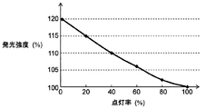
- FIG. 7 is a characteristic diagram showing an example of the relationship between the light emission intensity and the lighting rate according to Embodiment 1 of the present invention.
- FIG. 1 is an exploded perspective view showing the structure of the panel according to Embodiment 1 of the present invention.
- FIG. 2 is an electrode array diagram of the panel.
- FIG. 3 is a drive voltage waveform diagram applied to each electrode of the panel.
- FIG. 8 is a diagram for explaining a specific example regarding correction of image data based on the size of the partial lighting rate in the first embodiment of the present invention.
- FIG. 9 is a circuit block diagram showing an example of the configuration of the image signal processing circuit according to Embodiment 2 of the present invention.
- FIG. 10 is a diagram for explaining a specific example when the dithering process is changed based on the size of the partial lighting rate in the second embodiment of the present invention.
- FIG. 11 is a diagram for explaining another example when the dither processing is changed based on the size of the partial lighting rate in the second embodiment of the present invention.
- FIG. 1 is an exploded perspective view showing the structure of panel 10 according to Embodiment 1 of the present invention.
- a plurality of display electrode pairs 24 each including a scanning electrode 22 and a sustain electrode 23 are formed on a glass front plate 21.
- a dielectric layer 25 is formed so as to cover the scan electrode 22 and the sustain electrode 23, and a protective layer 26 is formed on the dielectric layer 25.
- the protective layer 26 has been used as a panel material in order to lower the discharge start voltage in the discharge cell, and has a large secondary electron emission coefficient and durability when neon (Ne) and xenon (Xe) gas is sealed. It is formed from a material mainly composed of MgO having excellent properties.
- a plurality of data electrodes 32 are formed on the back plate 31.
- a dielectric layer 33 is formed so as to cover the data electrode 32. Further, a cross-shaped partition wall 34 is formed thereon.
- a phosphor layer 35 that emits light of each color of red (R), green (G), and blue (B) is provided on the side surface of the partition wall 34 and on the dielectric layer 33.
- the front plate 21 and the back plate 31 are arranged to face each other so that the display electrode pair 24 and the data electrode 32 intersect with each other with a minute discharge space interposed therebetween. And the outer peripheral part is sealed with sealing materials, such as glass frit.
- a mixed gas of neon and xenon is sealed as a discharge gas in the discharge space inside.
- a discharge gas having a xenon partial pressure of about 10% is used in order to improve luminous efficiency.
- the discharge space is partitioned into a plurality of sections by partition walls 34, and discharge cells are formed at the intersections between the display electrode pairs 24 and the data electrodes 32. These discharge cells discharge and emit light to display an image.
- the structure of the panel 10 is not limited to the above-described structure, and may be, for example, provided with a stripe-shaped partition wall.
- the mixing ratio of the discharge gas is not limited to the above-described numerical values, and may be other mixing ratios.
- FIG. 2 is an electrode array diagram of panel 10 in accordance with the first exemplary embodiment of the present invention.
- panel 10 is driven by the subfield method.
- this subfield method one field is divided into a plurality of subfields on the time axis, and a luminance weight is set for each subfield. Then, gradation display is performed by controlling light emission / non-light emission of each discharge cell for each subfield.
- one field is composed of eight subfields (first SF, second SF,..., Eighth SF), and each subfield is, for example, (1, 2, 4, 8, 16). , 32, 64, and 128).
- the number of sustain pulses is generated by multiplying the luminance weight by a preset luminance magnification.
- the brightness of the image is adjusted by controlling the number of times of light emission in the sustain period.
- an all-cell initializing operation for generating an initializing discharge in all discharge cells is performed in the initializing period of one subfield, and the immediately preceding period is set in the initializing period of the other subfield.
- a selective initializing operation for selectively generating an initializing discharge is performed on the discharge cells that have undergone the sustain discharge in the subfield. By doing so, it is possible to reduce light emission not related to gradation display as much as possible and improve the contrast ratio.
- the all-cell initialization operation is performed in the initialization period of the first SF, and the selective initialization operation is performed in the initialization period of the second SF to the eighth SF.
- the light emission not related to the image display is only the light emission due to the discharge of the all-cell initializing operation in the first SF. Therefore, the black luminance, which is the luminance of the black display area where no sustain discharge is generated, is only weak light emission in the all-cell initialization operation, and an image display with high contrast is possible.
- the sustain period of each subfield the number of sustain pulses obtained by multiplying the luminance weight of each subfield by a predetermined luminance magnification is applied to each display electrode pair 24.
- the number of subfields and the luminance weight of each subfield are not limited to the above values shown in the present embodiment.
- the structure which switches a subfield structure based on an image signal etc. may be sufficient.
- the image signal processing circuit which will be described later, performs image data (emission / emission for each subfield) according to the size of the partial lighting rate for each subfield calculated by the partial lighting rate calculation unit described later. (Data indicating non-light emission) is changed. Thereby, each discharge cell in panel 10 is made to emit light with an appropriate light emission luminance corresponding to the image signal, and the image display quality is improved.
- image data emission / emission for each subfield
- FIG. 3 is a waveform diagram of driving voltage applied to each electrode of panel 10 in the first exemplary embodiment of the present invention.
- scan electrode SC1 that scans first in the address period
- scan electrode SCn that scans last in the address period
- sustain electrode SU1 to sustain electrode SUn for example, scan electrode SC1080
- data electrode D1 data electrode
- FIG. 6 shows driving waveforms of the data electrode Dm.
- FIG. 3 shows driving voltage waveforms of two subfields. That is, a first subfield (first SF) of a subfield for performing all-cell initialization operation (referred to as “all-cell initialization subfield”) and a subfield for performing selective initialization operation (“selection initialization subfield”)
- FIG. 3 shows a second subfield (second SF).
- the drive voltage waveform in the other subfields is substantially the same as the drive voltage waveform of the second SF except that the number of sustain pulses generated in the sustain period is different.
- scan electrode SCi, sustain electrode SUi, and data electrode Dk in the following represent electrodes selected from the respective electrodes based on image data.
- the first SF which is an all-cell initialization subfield, will be described.
- 0 (V) is applied to each of the data electrode D1 to the data electrode Dm and the sustain electrode SU1 to the sustain electrode SUn.
- a voltage Vi1 is applied to scan electrode SC1 through scan electrode SCn from 0 (V), and a ramp waveform voltage (hereinafter referred to as “up-ramp waveform”) that gradually rises from voltage Vi1 toward voltage Vi2.
- up-ramp waveform a ramp waveform voltage that gradually rises from voltage Vi1 toward voltage Vi2.
- This voltage Vi1 is a voltage equal to or lower than the discharge start voltage
- voltage Vi2 is a voltage exceeding the discharge start voltage with respect to sustain electrode SU1 through sustain electrode SUn.
- Vd a positive write pulse voltage
- a positive write pulse voltage Vd is applied to.
- the voltage difference at the intersection between the data electrode Dk and the scan electrode SC1 is the difference between the wall voltage on the data electrode Dk and the wall voltage on the scan electrode SC1 due to the difference between the externally applied voltages (Vd ⁇ Va). It becomes the sum and exceeds the discharge start voltage. As a result, a discharge is generated between data electrode Dk and scan electrode SC1.
- the voltage difference between sustain electrode SU1 and scan electrode SC1 is the difference between externally applied voltages (Ve2-Va) and sustain electrode SU1.
- the difference between the upper wall voltage and the wall voltage on the scan electrode SC1 is added.
- the sustain electrode SU1 and the scan electrode SC1 are not easily discharged but are likely to be discharged. Can do.
- the discharge generated between data electrode Dk and scan electrode SC1 can be triggered to generate a discharge between sustain electrode SU1 and scan electrode SC1 in the region intersecting with data electrode Dk.
- address discharge occurs in the discharge cells to be lit.
- a positive wall voltage is accumulated on scan electrode SC1
- a negative wall voltage is accumulated on sustain electrode SU1
- a negative wall voltage is also accumulated on data electrode Dk.
- the address operation is performed in which the address discharge is caused in the discharge cells to be lit in the first row and the wall voltage is accumulated on each electrode.
- the voltage at the intersection of data electrode D1 to data electrode Dm and scan electrode SC1 to which address pulse voltage Vd has not been applied does not exceed the discharge start voltage, so address discharge does not occur.
- the above address operation is sequentially performed until the discharge cell in the nth row, and the address period ends.
- sustain pulses of the number obtained by multiplying the luminance weight by a predetermined luminance magnification are alternately applied to the display electrode pair 24 to generate a sustain discharge in the discharge cell that generated the address discharge, and the discharge cell emits light.
- a sustain discharge occurs between scan electrode SCi and sustain electrode SUi, and phosphor layer 35 emits light due to the ultraviolet rays generated at this time. Then, a negative wall voltage is accumulated on scan electrode SCi, and a positive wall voltage is accumulated on sustain electrode SUi. Further, a positive wall voltage is accumulated on the data electrode Dk. In the discharge cells in which no address discharge has occurred during the address period, no sustain discharge occurs, and the wall voltage at the end of the initialization period is maintained.
- sustain pulses of the number obtained by multiplying the luminance weight by the luminance magnification are alternately applied to scan electrode SC1 through scan electrode SCn and sustain electrode SU1 through sustain electrode SUn, thereby giving a potential difference between the electrodes of display electrode pair 24. .
- the sustain discharge is continuously performed in the discharge cells that have caused the address discharge in the address period.
- the ramp waveform voltage increases from 0 (V), which is the base potential, toward the voltage Vers exceeding the discharge start voltage.
- L3 (hereinafter referred to as “erase ramp waveform”) is applied to scan electrode SC1 through scan electrode SCn.
- erase discharge a weak discharge (hereinafter referred to as “erase discharge”) occurs between sustain electrode SUi and scan electrode SCi of the discharge cell in which the sustain discharge has occurred.
- the charged particles generated by the erasing discharge are accumulated as wall charges on the sustain electrode SUi and the scan electrode SCi so as to alleviate the voltage difference between the sustain electrode SUi and the scan electrode SCi.
- the wall voltage on the scan electrode SCi and the sustain electrode SUi remains the difference between the voltage applied to the scan electrode SCi and the discharge start voltage, that is, (voltage Vers ⁇ discharge) while leaving the positive wall charge on the data electrode Dk. It is weakened to the extent of the starting voltage.
- scan electrode SC1 to scan electrode SCn are returned to 0 (V), and the sustain operation in the sustain period ends.
- a drive voltage waveform in which the first half of the initialization period in the first SF is omitted is applied to each electrode. That is, voltage Ve1 is applied to sustain electrode SU1 through sustain electrode SUn, and 0 (V) is applied to data electrode D1 through data electrode Dm. Then, a down-ramp waveform L4 that gently falls from scan voltage SC1 to scan electrode SCn to a voltage equal to or lower than the discharge start voltage (for example, 0 (V)) toward negative voltage Vi4 is applied.
- the initializing operation in the second SF is a selective initializing operation in which the initializing discharge is performed on the discharge cells in which the sustain operation has been performed in the sustain period of the immediately preceding subfield.
- the drive waveforms similar to those in the first SF address period are applied to scan electrode SC1 through scan electrode SCn, sustain electrode SU1 through sustain electrode SUn, and data electrode D1 through data electrode Dm.
- a predetermined number of sustain pulses are alternately applied to scan electrode SC1 through scan electrode SCn and sustain electrode SU1 through sustain electrode SUn.
- a sustain discharge is generated in the discharge cells that have generated the address discharge in the address period.
- the number of sustain pulses generated in the sustain period is different from that of scan electrode SC1 through scan electrode SCn, sustain electrode SU1 through sustain electrode SUn, and data electrode D1 through data electrode Dm.
- a drive waveform similar to 2SF is applied.
- FIG. 4 is a circuit block diagram of plasma display device 1 according to the first exemplary embodiment of the present invention.
- the plasma display apparatus 1 includes a panel 10, an image signal processing circuit 41, a data electrode drive circuit 42, a scan electrode drive circuit 43, a sustain electrode drive circuit 44, a timing generation circuit 45, and a power supply circuit that supplies necessary power to each circuit block. (Not shown).
- the image signal processing circuit 41 emits the input image signal sig for each subfield according to the number of discharge cells of the panel 10 in order to cause the discharge cells to emit light with brightness according to the gradation value of the image signal sig. ⁇ Convert to image data indicating non-light emission.
- the image signal processing circuit 41 in the present embodiment has a preset subfield configuration (this subfield configuration is the number of subfields constituting one field, the arrangement of each subfield, and each subfield. And the minimum gradation value (for example, gradation value “0”) set in the plasma display device 1 to the maximum gradation value (for example, gradation value “255”).
- coding table a table in which the gradation values up to and the coding data set for each gradation value (data indicating light emission / non-light emission in each subfield) are set. ing. Then, the image signal sig is converted into image data based on the coding table.
- the image signal processing circuit 41 in the present embodiment calculates a partial lighting rate described later, and image data indicating light emission / non-light emission for each subfield of the discharge cell according to the calculated partial lighting rate.
- the luminance weight is corrected based on the size of the partial lighting rate to obtain a corrected luminance weight, and the image data so that the gradation value calculated based on the corrected luminance weight becomes the gradation value to be displayed.
- the discharge cell is caused to emit light with an appropriate luminance according to the image signal, an unnatural luminance change of the image displayed on the panel 10 is prevented, and the image display quality is improved. Details thereof will be described later.
- the data electrode driving circuit 42 converts the image data for each subfield into signals corresponding to the data electrodes D1 to Dm. Then, the data electrodes D1 to Dm are driven based on the timing signal.
- the timing generation circuit 45 generates various timing signals for controlling the operation of each circuit block based on outputs from the horizontal synchronization signal H and the vertical synchronization signal V, and each circuit block (image signal processing circuit 41, data electrode drive). Circuit 42, scan electrode drive circuit 43, and sustain electrode drive circuit 44).
- Scan electrode drive circuit 43 includes an initialization waveform generation circuit (not shown), a scan pulse generation circuit (not shown), and sustain pulse generation circuit 50.
- the initialization waveform generation circuit generates an initialization waveform to be applied to scan electrode SC1 through scan electrode SCn in the initialization period.
- the scan pulse generating circuit includes a plurality of scan ICs and generates scan pulses to be applied to scan electrode SC1 through scan electrode SCn in the address period.
- Sustain pulse generation circuit 50 generates a sustain pulse to be applied to scan electrode SC1 through scan electrode SCn in the sustain period.
- Scan electrode drive circuit 43 drives each of scan electrode SC1 through scan electrode SCn based on the timing signal.
- Sustain electrode drive circuit 44 includes sustain pulse generation circuit 60 and a circuit (not shown) for generating voltage Ve1 and voltage Ve2. Then, sustain electrode SU1 to sustain electrode SUn are driven based on the timing signal.
- FIG. 5 is a circuit diagram of sustain pulse generation circuit 50 and sustain pulse generation circuit 60 in the first exemplary embodiment of the present invention.
- the interelectrode capacitance of the panel 10 is shown as Cp, and the circuit for generating the scan pulse and the initialization voltage waveform is omitted.
- the sustain pulse generation circuit 50 includes a power recovery circuit 51 and a clamp circuit 52.
- the power recovery circuit 51 and the clamp circuit 52 are connected to the scan electrodes SC1 to SCn that are one end of the interelectrode capacitance Cp of the panel 10 via a scan pulse generation circuit (not shown because it is in a short circuit state during the sustain period). It is connected.
- the power recovery circuit 51 has a power recovery capacitor C10, a switching element Q11, a switching element Q12, a backflow prevention diode D11, a backflow prevention diode D12, and a resonance inductor L10. Then, the interelectrode capacitance Cp and the inductor L10 are LC-resonated to cause the sustain pulse to rise and fall. Thus, the power recovery circuit 51 drives the scan electrodes SC1 to SCn by LC resonance without being supplied with power from the power source. Therefore, although the output impedance is higher than that of the clamp circuit 52, the power consumption is ideally zero.
- the power recovery capacitor C10 has a sufficiently large capacity compared to the interelectrode capacity Cp, and is charged to about Vs / 2, which is half of the voltage value Vs, so as to serve as a power source for the power recovery circuit 51.
- Clamp circuit 52 includes switching element Q13 for clamping scan electrode SC1 through scan electrode SCn to voltage Vs, and switching element Q14 for clamping scan electrode SC1 through scan electrode SCn to the base potential of 0 (V). is doing. Then, scan electrode SC1 to scan electrode SCn are connected to power supply VS via switching element Q13 and clamped to voltage Vs. Further, scan electrode SC1 to scan electrode SCn are grounded via switching element Q14 and clamped to 0 (V). Therefore, the impedance at the time of voltage application by the clamp circuit 52 is small, and a large discharge current due to strong sustain discharge can flow stably.
- Sustain pulse generation circuit 50 is connected to power recovery circuit 51 by clamping switching element Q11, switching element Q12, switching element Q13, and switching element Q14 in accordance with a timing signal output from timing generation circuit 45.
- the circuit 52 is operated to generate a sustain pulse waveform. In FIG. 5, details of the signal path of the timing signal are omitted.
- the switching element Q11 is turned on to cause the interelectrode capacitance Cp and the inductor L10 to resonate, and the power recovery capacitor C10 scans the scanning electrode through the switching element Q11, the diode D11, and the inductor L10. Power is supplied to SC1 through scan electrode SCn.
- switching element Q13 is turned on, and the circuit for driving scan electrode SC1 through scan electrode SCn is switched from power recovery circuit 51 to clamp circuit 52. Scan electrode SC1 through scan electrode SCn are clamped to voltage Vs.
- the switching element Q12 is turned on to resonate the interelectrode capacitance Cp and the inductor L10, and the interelectrode capacitance Cp is used for power recovery through the inductor L10, the diode D12, and the switching element Q12.
- the power is recovered in the capacitor C10.
- switching element Q14 is turned on, and a circuit for driving scan electrode SC1 through scan electrode SCn is connected from power recovery circuit 51 to clamp circuit 52.
- the scan electrodes SC1 to SCn are clamped to 0 (V) which is the base potential.
- sustain pulse generating circuit 50 generates a sustain pulse.
- switching elements can be configured using generally known elements such as a MOSFET (Metal Oxide Semiconductor Field Effect Transistor) and an IGBT (Insulated Gate Bipolar Transistor).
- MOSFET Metal Oxide Semiconductor Field Effect Transistor
- IGBT Insulated Gate Bipolar Transistor
- Sustain pulse generation circuit 60 has substantially the same configuration as sustain pulse generation circuit 50, and includes a power recovery circuit 61 and a clamp circuit 62.
- the power recovery circuit 61 includes a power recovery capacitor C20, a switching element Q21, a switching element Q22, a backflow prevention diode D21, a backflow prevention diode D22, and a resonance inductor L20. Electric power for driving sustain electrode SU1 through sustain electrode SUn is recovered and reused.
- Clamp circuit 62 includes switching element Q23 for clamping sustain electrode SU1 through sustain electrode SUn to voltage Vs, and switching element Q24 for clamping sustain electrode SU1 through sustain electrode SUn to the ground potential (0 (V)). Have.
- Sustain pulse generating circuit 60 is connected to sustain electrode SU1 through sustain electrode SUn, which is one end of interelectrode capacitance Cp of panel 10.
- the operation of sustain pulse generating circuit 60 is the same as that of sustain pulse generating circuit 50, and therefore description thereof is omitted.
- FIG. 5 also shows a power source VE1 that generates the voltage Ve1, a switching element Q26 for applying the voltage Ve1 to the sustain electrodes SU1 to SUn, a switching element Q27, a power source ⁇ VE that generates the voltage ⁇ Ve, and a backflow prevention A diode D30, a charge pump capacitor C30 for stacking the voltage ⁇ Ve on the voltage Ve1, a switching element Q28 and a switching element Q29 for stacking the voltage ⁇ Ve on the voltage Ve1 to obtain the voltage Ve2 are shown.
- the switching element Q26 and the switching element Q27 are turned on to connect the sustain electrode SU1 to the sustain electrode SUn to the positive voltage via the diode D30, the switching element Q26, and the switching element Q27. Ve1 is applied. At this time, the switching element Q28 is turned on and charged so that the voltage of the capacitor C30 becomes the voltage Ve1.
- the switching element Q26 and the switching element Q27 are kept conductive, the switching element Q28 is cut off, and the switching element Q29 is turned on to apply the voltage ⁇ Ve to the voltage of the capacitor C30. Superimpose.
- the circuit to which the voltage Ve1 and the voltage Ve2 are applied is not limited to the circuit shown in FIG.
- a power source that generates the voltage Ve1 a power source that generates the voltage Ve2
- a plurality of switching elements for applying each voltage to the sustain electrodes SU1 to SUn are used to maintain each voltage at a necessary timing.
- a configuration may be adopted in which the electrodes are applied to the electrodes SU1 to SUn.
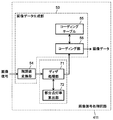
- FIG. 6 is a circuit block diagram showing an example of the configuration of the image signal processing circuit 41 according to Embodiment 1 of the present invention.
- FIG. 6 shows circuit blocks related to image data control in this embodiment, and other circuit blocks are omitted.
- the image signal processing circuit 41 includes an image data generation unit 53, a partial lighting rate calculation unit 58, a lookup table 57, and an image data change unit 59.
- the image data generation unit 53 generates image data based on the image signal.
- the partial lighting rate calculation unit 58 calculates the lighting rate for each display electrode pair 24 based on the image data output from the image data generation unit 53.
- the look-up table 57 stores the relationship between the brightness of light emission generated by one sustain discharge and the lighting rate as correction data.
- the image data changing unit 59 changes the image data output from the image data generating unit 53 based on the correction data read from the lookup table 57 to generate new image data.
- the image data generation unit 53 includes a gradation value conversion unit 54, a coding table 55, and a coding unit 56.
- the gradation value conversion unit 54 converts the image signal into an appropriate gradation value according to the magnitude of the image signal.
- the coding unit 56 reads the coding data from the coding table 55 based on the gradation value output from the gradation value conversion unit 54 and generates image data.
- the coding table 55 is configured by associating preset coding data with each gradation value and storing it in an arbitrarily readable storage element such as a semiconductor memory.
- the gradation value converter 54 outputs an appropriate gradation value according to the size of the image signal. For example, if the image signal has a magnitude corresponding to the gradation value “47”, the gradation value “47” is output. Alternatively, if the image signal has a magnitude corresponding to the gradation value “119”, the gradation value “119” is output.
- the coding unit 56 reads the coding data from the coding table 55 based on the gradation value output from the gradation value conversion unit 54. For example, when the gradation value “47” is output from the gradation value converter 54, “1, 1, 1, 1, 0, 1, 0, 0” is displayed in each subfield from the first SF to the eighth SF. Is read from the coding table 55. For example, when the gradation value “119” is output from the gradation value conversion unit 54, the coding data “1, 1, 1, 0, 1, 1, 1, 0” is similarly read out. Then, the read coding data is output to the subsequent stage as image data. Note that “1” represents a subfield in which writing is performed, that is, a light emitting subfield, and “0” represents a subfield in which writing is not performed, that is, a non-light emitting subfield.
- the image data generation unit 53 generates image data from the image signal in this way.
- the partial lighting rate calculation unit 58 determines the ratio of the number of discharge cells to be lit to the total number of discharge cells formed on one display electrode pair 24 based on the image data output from the image data generation unit 53. The rate is calculated for each display electrode pair 24 and for each subfield.
- the image data changing unit 59 reads the correction data from the lookup table 57 based on the size of the partial lighting rate calculated by the partial lighting rate calculating unit 58. Then, the image data is changed based on the read correction data, and new image data is generated and output.
- the plasma display device 1 causes each discharge cell to emit light with an appropriate light emission luminance according to the image signal, with such a configuration. And the unnatural brightness
- the brightness of light emission generated by one sustain discharge is referred to as “light emission intensity”.
- the brightness of the light emission that changes based on the number of occurrences of the sustain discharge in one field is referred to as “light emission luminance”.
- FIG. 7 is a characteristic diagram showing an example of the relationship between the light emission intensity and the lighting rate in Embodiment 1 of the present invention.
- the horizontal axis represents the lighting rate
- the vertical axis represents the change in emission intensity in one discharge cell. Note that the change in emission intensity on the vertical axis is based on the emission intensity at a lighting rate of 100% as a reference, and indicates the percentage of the change in emission intensity compared to the emission intensity.
- the emission intensity varies depending on the lighting rate, and the emission intensity increases as the lighting rate decreases. For example, in the characteristics shown in FIG. 7, when the lighting rate becomes 1%, the emission intensity increases by 20% compared to when the lighting rate is 100%. This is considered due to the following reasons.
- the output impedance of the power recovery circuit is larger than the output impedance of the clamp circuit. Therefore, if the load during driving changes, the waveform shape of the sustain pulse rises easily. For example, when the driving load increases, the rising waveform shape becomes gradual, and conversely when the driving load decreases, the rising waveform shape becomes steep. Further, when the output impedance is large, the voltage drop when the drive impedance is increased is also increased.
- the sustain discharge is generated with a large change in the voltage applied to the discharge cell.
- a sustain discharge that is stronger than a sustain discharge that occurs with a gradual rise and a relatively small change in the voltage applied to the discharge cell occurs.
- the discharge intensity of the sustain discharge changes depending on the waveform shape of the rise of the sustain pulse. When a strong sustain discharge is generated, the emission intensity is higher than when a weak sustain discharge is generated.
- the load during driving decreases as the lighting rate decreases.
- the waveform shape of the rising edge of the sustain pulse becomes steep and a strong sustain discharge is generated. This is considered to be the reason why the emission intensity increases when the lighting rate is low.
- the difference in voltage drop also causes a difference in discharge intensity and a difference in light emission luminance.
- the discharge cells to which the same gradation value is assigned emit light with different light emission luminances, thereby deteriorating the image display quality.
- the discharge cells can be made to emit light with an appropriate emission luminance corresponding to the image signal.
- the relationship between the lighting rate and the light emission intensity is measured in advance as shown in FIG. Then, the measurement result is stored in the lookup table as correction data. Then, the lighting rate is calculated, the correction data is read from the lookup table based on the calculated lighting rate, and the image data is changed.
- the discharge cell emits light with an appropriate luminance according to the image signal, an unnatural luminance change of the image displayed on the panel 10 is prevented, and the image display quality is improved.
- the accuracy of the calculated lighting rate is low, the accuracy of correction applied to the image data is also low.
- the lighting rate is calculated over the entire display area of the panel 10, even if there is a region where the lighting rate is extremely low, if the overall lighting rate is high, the average value of the entire display area of the panel 10 is obtained. A high lighting rate is calculated. If it does so, the area
- sustain pulses having substantially the same waveform shape are applied to the discharge cells formed on the same display electrode pair 24. Therefore, if the partial lighting rate is calculated with a region formed by all the discharge cells on one display electrode pair 24 as one region, the accuracy of correction applied to the gradation value can be increased.
- the partial lighting rate calculation unit 58 uses the ratio of the number of discharge cells to be lit with respect to the total number of discharge cells formed on one display electrode pair 24 as the partial lighting rate. The calculation is made every 24 and every subfield. Then, a correction to be added to the image data is calculated from the calculated partial lighting rate and the relationship between the lighting rate and the emission intensity measured in advance, and the image data is corrected.
- the relationship between the lighting rate and the emission intensity is measured in advance. Then, the measurement result, that is, the change in emission intensity corresponding to the lighting rate is stored in the lookup table 57 as correction data.
- the image data changing unit 59 reads correction data from the lookup table 57 based on the size of the partial lighting rate calculated by the partial lighting rate calculating unit 58. Then, a correction value to be added to the image data is calculated from the read correction data. Based on the calculation result, the image data output from the image data generation unit 53 is corrected.
- the discharge cell emits light with an appropriate light emission luminance according to the image signal, and the image display quality is improved.
- FIG. 8 is a diagram for explaining a specific example regarding correction of image data based on the size of the partial lighting rate in the first embodiment of the present invention.
- one field includes eight subfields from the first SF to the eighth SF, and each subfield has a luminance weight of (1, 2, 4, 8, 16, 32, 64, 128). Shall. Further, it is assumed that the lighting rate and the light emission intensity have the relationship shown in FIG.
- the partial lighting rate calculated by the partial lighting rate calculation unit 58 is 100% from the first SF to the fourth SF, 40% from the fifth SF and the sixth SF, It is assumed that the seventh SF and the eighth SF are 1%.
- the emission intensity is 100% at a partial lighting rate of 100%
- the emission intensity is 110% at a partial lighting rate of 40%
- the emission intensity is 120% at a partial lighting rate of 1%. It is. Therefore, based on the characteristics shown in FIG.
- the emission intensity of each subfield (the emission intensity when the lighting rate is 100% is 100%) is 100% from the first SF to the fourth SF
- the fifth SF and the sixth SF are 110%
- the seventh SF and the eighth SF are 120%.
- the corrected luminance weight obtained by multiplying the luminance weight of each subfield by the light emission intensity is obtained by multiplying each luminance weight (1, 2, 4, 8) by 1 (1, 2, 4, 8) from the first SF to the fourth SF. 8)
- the fifth SF and the sixth SF are 1.1 times the luminance weights (16, 32) (17.6, 35.2)
- the seventh SF and the eighth SF are the respective luminance weights (64, 128).
- Is multiplied by 1.2 (76.8, 153.6) That is, the corrected luminance weights from the first SF to the eighth SF are sequentially from the first SF as shown in FIG. 8 (1, 2, 4, 8, 17.6, 35.2, 76.8, 153.6). It becomes.
- the image data changing unit 59 changes the image data assigned to the discharge cells in the region A based on the corrected luminance weight.
- the image data when the gradation value “169” is to be displayed is (1, 0, 0, 1, 0, 1, 0, 1 in order from the first SF).
- the luminance weight of the first SF is (1)
- the luminance weight of the fourth SF is (8)
- the luminance weight of the sixth SF is (32)
- the image data changing unit 59 changes the image data so that the sum of the corrected luminance weights becomes “169”.
- the corrected image data is sequentially displayed from the first SF (1, 1, 1, 1, 0, 0, 0, 1). That is, the image data (1, 0, 0, 1, 0, 1, 0, 1) is changed to image data (1, 1, 1, 1, 0, 0, 0, 1).
- the image data is changed according to the size of the partial lighting rate.
- the discharge cells in the region A can emit light with brightness substantially equal to the gradation value “169” to be displayed.
- the luminance weight of the fifth SF is (17.6)
- the luminance weight of the sixth SF is (35.2)
- the luminance weight of the seventh SF is (76.8).
- the image data changing unit 59 changes the image data so that the sum of the corrected luminance weights becomes “240”.
- the corrected image data is sequentially (0, 1, 0, 1, 0, 0, 1, 1). That is, the image data (0, 0, 0, 0, 1, 1, 1, 1) is changed to the image data (0, 1, 0, 1, 0, 0, 1, 1.
- the gradation value “240.4” can be displayed, thereby causing the discharge cells in the region A to emit light with brightness substantially equal to the gradation value “240” to be displayed. be able to.
- the ratio of the number of discharge cells to be lit to the total number of discharge cells formed on one display electrode pair 24 is set as a partial lighting rate for each display electrode pair 24 and each subfield. To calculate. Then, the corrected luminance weight is calculated from the calculated partial lighting rate and the relationship between the lighting rate and the emission intensity measured in advance. Then, the image data is changed so that the gradation value calculated based on the corrected luminance weight becomes the gradation value to be displayed.
- the gradation value when calculated with the luminance weight before correction and the image data before change and the gradation value when calculated with the corrected luminance weight and the image data after change based on the size of the partial lighting rate
- the image data is changed so that is substantially equal.
- the partial lighting The image data is changed so that the gradation value is smaller than when the rate is high.
- the partial lighting rate when the partial lighting rate is low, the light emission intensity increases compared to when the partial lighting rate is high. Therefore, by adopting a configuration in which the image data is changed according to the size of the partial lighting rate as described above, it is possible to obtain an appropriate light emission luminance according to the gradation value of the image signal regardless of the size of the partial lighting rate.
- the discharge cell can emit light. Thereby, an unnatural brightness change of the image displayed on the panel 10 can be prevented, and the image display quality in the plasma display device 1 can be improved.
- the dither processing is changed according to the size of the partial lighting rate.
- a configuration in which the discharge cell emits light with an appropriate light emission luminance according to the image signal will be described.
- FIG. 9 is a circuit block diagram showing an example of the configuration of the image signal processing circuit according to the second embodiment of the present invention.
- FIG. 9 shows circuit blocks related to the present embodiment, and other circuit blocks are omitted. The same components as those of the image signal processing circuit 41 shown in FIG.
- the image signal processing circuit 411 includes a dither processing unit 71 and a partial lighting rate calculation unit 72 in addition to the image data generation unit 53 shown in FIG.
- the coding table 55 in the present embodiment is composed of coding data in which the number of gradation values (hereinafter referred to as “display gradations”) that can be used for image display is limited. Accordingly, discontinuous gradation values are set in the coding table 55.
- the gradation value conversion unit 54 outputs a gradation value corresponding to the size of the image signal without being limited to the display gradation set in the coding table 55.
- the dither processing unit 71 At least two different gradation values are selected from the display gradations so that the value obtained by averaging at a predetermined ratio becomes equal to the gradation value to be displayed. Then, one of the selected gradation values is assigned to each of a plurality of discharge cells combined in a matrix (hereinafter referred to as “discharge cell group”) at the predetermined ratio described above. For example, in the coding table 55, the next largest gradation value after the gradation value “80” is “88”.
- the dither processing unit 71 in the present embodiment changes the dither processing according to the size of the partial lighting rate calculated by the partial lighting rate calculation unit 72. Specifically, at least one of the gradation value to be selected and the ratio when the selected gradation value is assigned to the discharge cell group is changed according to the size of the partial lighting rate.
- the partial lighting rate calculation unit 72 stores the gradation value and the image data in association with each other in a storage unit (not shown) provided therein so that the partial lighting rate can be calculated from the gradation value. ing. Based on the gradation value transmitted from the dither processing unit 71, the ratio of the number of discharge cells to be lit with respect to the total number of discharge cells formed on one display electrode pair 24 is used as a partial lighting rate. It is calculated every 24 and every subfield.
- FIG. 10 is a diagram for explaining a specific example when the dithering process is changed based on the size of the partial lighting rate in the second embodiment of the present invention.
- one field includes eight subfields from the first SF to the eighth SF, and each subfield has a luminance weight of (1, 2, 4, 8, 16, 32, 64, 128). Shall. Further, it is assumed that the lighting rate and the light emission intensity have the relationship shown in FIG.
- the partial lighting rate calculated by the partial lighting rate calculation unit 58 is 100% from the first SF to the fourth SF, 80% is the fifth SF, and the sixth SF is Assume that 60%, the seventh SF is 40%, and the eighth SF is 20%.
- the emission intensity of each subfield (the emission intensity when the lighting rate is 100% is 100%) is 100 from the first SF to the fourth SF. %,
- the fifth SF is 102%, the sixth SF is 106%, the seventh SF is 110%, and the eighth SF is 115%.
- the corrected luminance weight obtained by multiplying the luminance weight of each subfield by the light emission intensity is (1, 2, 4, 8, 16.32, 33.92, 70. 4, 147.2).
- the dither processing unit 71 in the present embodiment changes the dither processing based on the corrected luminance weight.
- the image data having the gradation value “96” is (0, 0, 0, 0, 0, 1, 1, 0) in order from the first SF, and the gradation value “112”.
- the dither processing unit 71 changes the dither processing so that the gradation value “96” is assigned to the discharge cell group at a ratio of 3 and the gradation value “112” is 1. By doing so, the gradation value displayed in a pseudo manner can be set to “108.4”. As a result, the discharge cells in the region B can emit light with brightness substantially equal to the gradation value “108” to be displayed.
- FIG. 11 is a diagram for explaining another example when the dithering process is changed based on the size of the partial lighting rate in the second embodiment of the present invention. Note that the subfield configuration and the relationship between the lighting rate and the light emission intensity are the same as those shown in the description of FIG.
- the partial lighting rate calculated by the partial lighting rate calculation unit 58 is 100% from the first SF to the third SF, 1% for the fourth SF, and 5% for the fifth SF. It is assumed that 20% and 1% from the sixth SF to the eighth SF.
- the emission intensity of each subfield is 100% from the first SF to the third SF, 120% for the fourth SF, 115% for the fifth SF, and 115% for the sixth SF.
- the eighth SF is 120%. Therefore, the corrected luminance weight obtained by multiplying the luminance weight of each subfield by the emission intensity is (1, 2, 4, 9.6, 18.4, 38.4, 76 in order from the first SF as shown in FIG. .8, 153.6).
- the image data having the gradation value “224” is (0, 0, 0, 0, 0, 1, 1, 1) in order from the first SF.
- the dither processing unit 71 if there is a gradation value at which the emission luminance calculated based on the corrected luminance weight is substantially equal to the gradation value “232”, Select the key value and output it to the subsequent stage.
- the dither processing unit 71 changes the dither processing if there is no gradation value at which the light emission luminance calculated based on the corrected luminance weight is substantially equal to the gradation value “232”.
- the gradation value to be displayed can be displayed by changing only the ratio of assigning the selected gradation value to the discharge cell group without changing the selected gradation value. It was. However, in the example shown in FIG. 11, the light emission luminance calculated based on the corrected luminance weight is a value larger than the gradation value “232” to be displayed at any gradation value. Therefore, the gradation value to be displayed cannot be displayed only by changing the ratio when the selected gradation value is assigned to the discharge cell group.
- the dither processing unit 71 changes the gradation value to be selected. For example, in the example shown in FIG. 11, the dither processing is performed so that the light emission luminance calculated based on the corrected luminance weight becomes a value close to the first selected gradation value “224” and gradation value “240”. The unit 71 changes the gradation value to be selected.
- the gradation value “188” and the gradation value “200” are included in the display gradation, and the image data of the gradation value “188” are sequentially (0, 0, 1, 1) from the first SF. 1, 1, 0, 1), and the image data having the gradation value “200” is (0, 0, 0, 1, 0, 0, 1, 1) in order from the first SF.
- the discharge cells in the region C are caused to emit light with the image data corresponding to the gradation value “188”
- the light emission luminance of the discharge cell in the above is equal to the gradation value “224”.
- the light emission luminance of the discharge cell has a brightness equal to the gradation value “240”.
- the dither processing unit 71 uses the gradation value “224” and the gradation value “240” as the gradation values at which the emission luminance calculated based on the corrected luminance weight is substantially equal to the gradation value “224”.
- the light emission luminance calculated based on “188” and the corrected luminance weight is changed to a gradation value “200” that is substantially equal to the gradation value “240”.
- the partial lighting rate is large.
- the dither processing is changed according to the situation. By doing so, it becomes possible to cause the discharge cell to emit light with an appropriate light emission luminance according to the image signal, to prevent an unnatural luminance change of the image displayed on the panel 10, and to improve the image display quality in the plasma display device 1. Can be improved.
- FIG. 10 illustrates an example of changing the ratio when the selected gradation value is assigned to the discharge cell group
- FIG. 11 illustrates an example of changing the selected gradation value
- the dither processing unit 71 in the present embodiment changes at least one of the gradation value to be selected and the ratio when assigning the selected gradation value to the discharge cell group according to the size of the partial lighting rate. It is characterized by. Therefore, a configuration in which the example shown in FIG. 10 and the example shown in FIG. 11 are used in combination may be used. In other words, the configuration may be such that changing the selected gradation value and changing the ratio when assigning the selected gradation value to the discharge cell group are performed simultaneously.
- the configuration in which the partial lighting rate is calculated using the region formed by all the discharge cells on one display electrode pair 24 as one region has been described. It is not limited to.
- the area for calculating the partial lighting rate may be set based on the number of output terminals of the IC that drives the scan electrode 22 or the number of output terminals of the IC that drives the sustain electrode 23.
- a region for calculating a partial lighting rate based on the discharge cell group is set. It is good.
- the discharge cell group is composed of discharge cells of 2 rows and 2 columns
- the partial lighting rate may be calculated with a region formed by all the discharge cells on the two display electrode pairs 24 as one region. .
- the scan electrode and the scan electrode are adjacent to each other, and the sustain electrode and the sustain electrode are adjacent to each other.
- the specific numerical values shown in the embodiment of the present invention are set based on the characteristics of a panel of 50 inches and 1080 pairs of display electrodes, and are merely examples of the embodiment. Absent.
- the present invention is not limited to these numerical values, and is desirably set optimally according to the characteristics of the panel, the specifications of the plasma display device, and the like. Each of these numerical values is allowed to vary within a range where the above-described effect can be obtained.
- the configuration in which the erase ramp waveform L3 is applied to scan electrode SC1 through scan electrode SCn has been described.
- the erase ramp waveform L3 is applied to sustain electrode SU1 through sustain electrode SUn. You can also.
- an erasing discharge may be generated not by the erasing ramp waveform L3 but by a so-called narrow erasing pulse.
- the discharge cells of the panel it is possible to cause the discharge cells of the panel to emit light with an appropriate light emission luminance according to the image signal by changing the image data based on the change in the light emission intensity caused by the fluctuation of the lighting rate. Therefore, it is useful as a plasma display device and a panel driving method capable of preventing an unnatural luminance change of an image displayed on the panel and improving the image display quality.
- Plasma display device 10 Panel (Plasma display panel) DESCRIPTION OF SYMBOLS 21 Front plate 22 Scan electrode 23 Sustain electrode 24 Display electrode pair 25,33 Dielectric layer 26 Protective layer 31 Back plate 32 Data electrode 34 Partition 35 Phosphor layer 41,411 Image signal processing circuit 42 Data electrode drive circuit 43 Scan electrode drive Circuit 44 Sustain electrode drive circuit 45 Timing generation circuit 50, 60 Sustain pulse generation circuit 51, 61 Power recovery circuit 52, 62 Clamp circuit 53 Image data generation unit 54 Tone value conversion unit 55 Coding table 56 Coding unit 57 Look-up table 58 72 Partial lighting rate calculation unit 59 Image data change unit 71 Dither processing unit C10, C20, C30 Capacitors Q11, Q12, Q13, Q14, Q21, Q22, Q23, Q24, Q26, Q27, Q28, Q29 Switching element 11, D12, D21, D22, D30 diode L10, L20 Inductor
Abstract
プラズマディスプレイパネルの放電セルを画像信号に応じた適正な輝度で発光させ、画像表示品質を向上させる。そのために、走査電極と維持電極とからなる表示電極対を有する放電セルを複数備えるプラズマディスプレイパネルと、放電セルを画像信号の階調値に応じた明るさで発光させるために、画像信号を放電セルにおけるサブフィールド毎の発光・非発光を示す画像データに変換する画像信号処理回路(41)を備え、画像信号処理回路(41)は、1つの表示電極対上に形成される全放電セル数に対する点灯させるべき放電セル数の割合を部分点灯率として表示電極対毎かつサブフィールド毎に算出する部分点灯率算出部(58)を有し、部分点灯率算出部(58)から出力される部分点灯率の大きさに応じて画像データを変更する。
Description
本発明は、壁掛けテレビや大型モニターに用いられるプラズマディスプレイ装置およびプラズマディスプレイパネルの駆動方法に関する。
プラズマディスプレイパネル(以下、「パネル」と略記する)として代表的な交流面放電型パネルは、対向配置された前面板と背面板との間に多数の放電セルが形成されている。前面板は、1対の走査電極と維持電極とからなる表示電極対が前面ガラス基板上に互いに平行に複数対形成されている。そして、それら表示電極対を覆うように誘電体層および保護層が形成されている。背面板は、背面ガラス基板上に複数の平行なデータ電極が形成され、それらデータ電極を覆うように誘電体層が形成され、さらにその上にデータ電極と平行に複数の隔壁が形成されている。そして、誘電体層の表面と隔壁の側面とに蛍光体層が形成されている。そして、表示電極対とデータ電極とが立体交差するように前面板と背面板とが対向配置されて密封されている。密封された内部の放電空間には、例えば分圧比で5%のキセノンを含む放電ガスが封入されている。ここで表示電極対とデータ電極とが対向する部分に放電セルが形成される。このような構成のパネルにおいて、各放電セル内でガス放電により紫外線を発生させ、この紫外線で赤色(R)、緑色(G)および青色(B)の各色の蛍光体を励起発光させてカラー表示を行っている。
パネルを駆動する方法としては一般にサブフィールド法が用いられている(例えば、特許文献1参照)。サブフィールド法では、1フィールドを複数のサブフィールドに分割し、それぞれのサブフィールドで各放電セルを発光または非発光させることにより階調表示を行う。各サブフィールドは、初期化期間、書込み期間および維持期間を有する。
初期化期間では、各走査電極に初期化波形を印加し、各放電セルで初期化放電を発生させる。それにより、各放電セルにおいて、続く書込み動作のために必要な壁電荷を形成する。
書込み期間では、走査電極に順次走査パルスを印加(以下、この動作を「走査」とも記す)するとともに、データ電極には表示すべき画像信号に対応した書込みパルスを印加する(以下、これらの動作を総称して「書込み」とも記す)。それにより、走査電極とデータ電極との間で選択的に書込み放電を発生させ、選択的に壁電荷を形成する。
続く維持期間では、表示させるべき輝度に応じた所定の数の維持パルスを走査電極と維持電極とからなる表示電極対に交互に印加する。それにより、書込み放電による壁電荷形成が行われた放電セルで選択的に放電を起こし、その放電セルを発光させる。これにより画像表示を行う。
複数の走査電極は走査電極駆動回路により駆動され、複数の維持電極は維持電極駆動回路により駆動され、複数のデータ電極はデータ電極駆動回路により駆動される。
このようなパネルを組み込んだプラズマディスプレイ装置では、その消費電力を削減するため、様々な消費電力削減技術が提案されている。
消費電力を削減する技術の一つとして、いわゆる電力回収回路が開示されている。電力回収回路では、パネルが容量性の負荷であることに着目し、インダクタを構成要素に含む共振回路によって、そのインダクタとパネルの負荷容量とをLC共振させる。そして、パネルの負荷容量に蓄えられた電力を電力回収用のコンデンサに回収し、回収した電力をパネルの駆動に再利用する(例えば、特許文献2参照)。
この技術では、例えば、維持期間における走査電極および維持電極への維持パルス電圧の印加にパネルから回収した電力を再利用し、維持期間に消費される電力を削減することで、消費電力の削減を実現することができる。
近年においては、パネルの大画面化、高精細化が進められており、それにともないプラズマディスプレイ装置におけるさらなる表示品質の向上が望まれている。
一方、パネルの大画面化、高精細化により、パネルにおける電極間容量や電極線のインピーダンスが増大し、パネルの駆動インピーダンスは増大する傾向にある。パネルの駆動インピーダンスが増大すると、点灯率(画像表示面を構成する放電セルの数に対する点灯すべき放電セルの割合)の変化により生じる駆動インピーダンスの変動が大きくなる。そのため、パネルの駆動回路から発生させる駆動波形に変動が生じやすくなる。
例えば、維持パルス発生回路においては、駆動インピーダンスが下がると維持パルスの立ち上がりが急峻になり、駆動インピーダンスが上がると維持パルスの立ち上がりが緩やかになる傾向にある。また、駆動インピーダンスが上がると、その分、電圧降下も大きくなる。
そして、維持パルスの立ち上がりが急峻になると、維持パルスの立ち上がりが緩やかなときと比較して、強い維持放電が発生しやすい。強い維持放電が発生すると、弱い維持放電が発生したときよりも発光輝度が高くなる。また、電圧降下の差も放電強度に差を生じさせ、発光輝度に差を生じさせる。そのため、点灯率が低いときと点灯率が高いときとで発光輝度に差が生じ、同じ階調値であるにもかかわらず発光輝度に差が生じることがある。そして、このような発光輝度の差は、パネルに表示される画像の不自然な輝度変化を発生させ、画像表示品質を劣化させる一因となる。
本発明のプラズマディスプレイ装置は、初期化期間と書込み期間と維持期間とを有するサブフィールドを1フィールド内に複数設けるサブフィールド法により駆動され、走査電極と維持電極とからなる表示電極対を有する放電セルを複数備えるパネルと、放電セルを画像信号の階調値に応じた明るさで発光させるために、画像信号を放電セルにおけるサブフィールド毎の発光・非発光を示す画像データに変換する画像信号処理回路とを備え、画像信号処理回路は、1つの表示電極対上に形成される全放電セル数に対する点灯させるべき放電セル数の割合を部分点灯率として表示電極対毎かつサブフィールド毎に算出する部分点灯率算出部を有し、部分点灯率算出部から出力される部分点灯率の大きさに応じて画像データを変更することを特徴とする。
これにより、放電セルを画像信号に応じた適正な輝度で発光させ、パネルに表示される画像の不自然な輝度変化を防止し、画像表示品質を向上させることが可能となる。
以下、本発明の実施の形態におけるプラズマディスプレイ装置について、図面を用いて説明する。
(実施の形態1)
図1は、本発明の実施の形態1におけるパネル10の構造を示す分解斜視図である。ガラス製の前面板21上には、走査電極22と維持電極23とからなる表示電極対24が複数形成されている。そして走査電極22と維持電極23とを覆うように誘電体層25が形成され、その誘電体層25上に保護層26が形成されている。
図1は、本発明の実施の形態1におけるパネル10の構造を示す分解斜視図である。ガラス製の前面板21上には、走査電極22と維持電極23とからなる表示電極対24が複数形成されている。そして走査電極22と維持電極23とを覆うように誘電体層25が形成され、その誘電体層25上に保護層26が形成されている。
また、保護層26は、放電セルにおける放電開始電圧を下げるために、パネルの材料として使用実績があり、ネオン(Ne)およびキセノン(Xe)ガスを封入した場合に2次電子放出係数が大きく耐久性に優れたMgOを主成分とする材料から形成されている。
背面板31上にはデータ電極32が複数形成されている。そして、データ電極32を覆うように誘電体層33が形成されている。そして、さらにその上に井桁状の隔壁34が形成されている。そして、隔壁34の側面および誘電体層33上には赤色(R)、緑色(G)および青色(B)の各色に発光する蛍光体層35が設けられている。
これら前面板21と背面板31とは、微小な放電空間を挟んで表示電極対24とデータ電極32とが交差するように対向配置されている。そして、その外周部をガラスフリット等の封着材によって封着されている。そして、その内部の放電空間には、ネオンとキセノンの混合ガスが放電ガスとして封入されている。なお、本実施の形態では、発光効率を向上させるためにキセノン分圧を約10%とした放電ガスを用いている。放電空間は隔壁34によって複数の区画に仕切られており、表示電極対24とデータ電極32とが交差する部分に放電セルが形成されている。そしてこれらの放電セルが放電、発光することにより画像が表示される。
なお、パネル10の構造は上述したものに限られるわけではなく、例えばストライプ状の隔壁を備えたものであってもよい。また、放電ガスの混合比率も上述した数値に限られるわけではなく、その他の混合比率であってもよい。
図2は、本発明の実施の形態1におけるパネル10の電極配列図である。パネル10には、行方向に延長されたn本の走査電極SC1~走査電極SCn(図1の走査電極22)およびn本の維持電極SU1~維持電極SUn(図1の維持電極23)が配列されている。そして、列方向に延長されたm本のデータ電極D1~データ電極Dm(図1のデータ電極32)が配列されている。そして、1対の走査電極SCi(i=1~n)および維持電極SUiと1つのデータ電極Dj(j=1~m)とが交差した部分に放電セルが形成されている。したがって、放電セルは放電空間内にm×n個形成されている。そして、m×n個の放電セルが形成された領域がパネル10の表示領域となる。
次に、パネル10を駆動するための駆動電圧波形とその動作の概要について図3を用いて説明する。なお、本実施の形態におけるプラズマディスプレイ装置は、サブフィールド法によってパネル10を駆動するものとする。このサブフィールド法では、1フィールドを時間軸上で複数のサブフィールドに分割し、各サブフィールドに輝度重みをそれぞれ設定する。そして、サブフィールド毎に各放電セルの発光・非発光を制御することによって階調表示を行う。
このサブフィールド法では、例えば、1フィールドを8のサブフィールド(第1SF、第2SF、・・・、第8SF)で構成し、各サブフィールドはそれぞれ、例えば(1、2、4、8、16、32、64、128)の輝度重みを有する構成とすることができる。そして、各サブフィールドでは、この輝度重みに、あらかじめ設定された輝度倍率を乗じた数の維持パルスを発生させる。これにより、維持期間における発光の回数を制御して画像の明るさを調整する。また、複数のサブフィールドのうち、1つのサブフィールドの初期化期間においては全ての放電セルに初期化放電を発生させる全セル初期化動作を行い、他のサブフィールドの初期化期間においては直前のサブフィールドで維持放電を行った放電セルに対して選択的に初期化放電を発生させる選択初期化動作を行う。こうすることで、階調表示に関係しない発光を極力減らしコントラスト比を向上させることが可能である。
そして、本実施の形態では、第1SFの初期化期間では全セル初期化動作を行い、第2SF~第8SFの初期化期間では選択初期化動作を行うものとする。これにより、画像の表示に関係のない発光は第1SFにおける全セル初期化動作の放電にともなう発光のみとなる。したがって、維持放電を発生させない黒表示領域の輝度である黒輝度は全セル初期化動作における微弱発光だけとなって、コントラストの高い画像表示が可能となる。また、各サブフィールドの維持期間においては、それぞれのサブフィールドの輝度重みに所定の輝度倍率を乗じた数の維持パルスを表示電極対24のそれぞれに印加する。
しかし、本発明は、サブフィールド数や各サブフィールドの輝度重みが、本実施の形態に示す上記の値に限定されるものではない。また、画像信号等にもとづいてサブフィールド構成を切換える構成であってもよい。
なお、本実施の形態では、後述する画像信号処理回路は、後述する部分点灯率算出部で算出されるサブフィールド毎の部分点灯率の大きさに応じて、画像データ(サブフィールド毎の発光・非発光を示すデータ)を変更している。これにより、パネル10において各放電セルを画像信号に応じた適正な発光輝度で発光させ、画像表示品質を向上させている。以下、まず駆動電圧波形の概要および駆動回路の構成について説明し、続いて、点灯率の大きさに応じた階調値の制御について説明する。
図3は、本発明の実施の形態1におけるパネル10の各電極に印加する駆動電圧波形図である。
なお、図3には、書込み期間において最初に走査を行う走査電極SC1、書込み期間において最後に走査を行う走査電極SCn(例えば、走査電極SC1080)、維持電極SU1~維持電極SUn、およびデータ電極D1~データ電極Dmの駆動波形を示す。
また、図3には、2つのサブフィールドの駆動電圧波形を示す。すなわち全セル初期化動作を行うサブフィールド(「全セル初期化サブフィールド」と呼称する)の第1サブフィールド(第1SF)と、選択初期化動作を行うサブフィールド(「選択初期化サブフィールド」と呼称する)の第2サブフィールド(第2SF)とを図3に示す。なお、他のサブフィールドにおける駆動電圧波形は、維持期間における維持パルスの発生数が異なる以外は第2SFの駆動電圧波形とほぼ同様である。また、以下における走査電極SCi、維持電極SUi、データ電極Dkは、各電極の中から画像データにもとづき選択された電極を表す。
まず、全セル初期化サブフィールドである第1SFについて説明する。
第1SFの初期化期間前半部では、データ電極D1~データ電極Dm、維持電極SU1~維持電極SUnにそれぞれ0(V)を印加する。そして、走査電極SC1~走査電極SCnには、0(V)から電圧Vi1を印加し、さらに電圧Vi1から、電圧Vi2に向かって緩やかに上昇する傾斜波形電圧(以下、「上りランプ波形」と呼称する)L1を印加する。この電圧Vi1は放電開始電圧以下の電圧であり、電圧Vi2は維持電極SU1~維持電極SUnに対して放電開始電圧を超える電圧である。
この上りランプ波形L1が上昇する間に、走査電極SC1~走査電極SCnと維持電極SU1~維持電極SUnとの間、および走査電極SC1~走査電極SCnとデータ電極D1~データ電極Dmとの間でそれぞれ微弱な初期化放電が持続して起こる。そして、走査電極SC1~走査電極SCn上部に負の壁電圧が蓄積されるとともに、データ電極D1~データ電極Dm上部および維持電極SU1~維持電極SUn上部には正の壁電圧が蓄積される。この電極上部の壁電圧とは、電極を覆う誘電体層上、保護層上、蛍光体層上等に蓄積された壁電荷により生じる電圧を表す。
初期化期間後半部では、維持電極SU1~維持電極SUnには正の電圧Ve1を印加し、データ電極D1~データ電極Dmには0(V)を印加する。そして、走査電極SC1~走査電極SCnには、電圧Vi3から負の電圧Vi4に向かって緩やかに下降する下り傾斜波形電圧(以下、「下りランプ波形」と呼称する)L2を印加する。この電圧Vi3は維持電極SU1~維持電極SUnに対して放電開始電圧以下となる電圧であり、電圧Vi4は放電開始電圧を超える電圧である。
この間に、走査電極SC1~走査電極SCnと維持電極SU1~維持電極SUnとの間、および走査電極SC1~走査電極SCnとデータ電極D1~データ電極Dmとの間でそれぞれ微弱な初期化放電が起こる。そして、走査電極SC1~走査電極SCn上部の負の壁電圧および維持電極SU1~維持電極SUn上部の正の壁電圧が弱められる。そして、データ電極D1~データ電極Dm上部の正の壁電圧は書込み動作に適した値に調整される。以上により、全ての放電セルに対して初期化放電を行う全セル初期化動作が終了する。
続く書込み期間では、走査電極SC1~走査電極SCnに対しては順次走査パルス電圧を印加し、データ電極D1~データ電極Dmに対しては発光させるべき放電セルに対応するデータ電極Dk(k=1~m)に正の書込みパルス電圧Vdを印加する。こうして、各放電セルに選択的に書込み放電を発生させる。
この書込み期間では、まず維持電極SU1~維持電極SUnに電圧Ve2を印加し、走査電極SC1~走査電極SCnに電圧Vc(Vc=Va+Vscn)を印加する。
そして、1行目の走査電極SC1に負の走査パルス電圧Vaを印加するとともに、データ電極D1~データ電極Dmのうち1行目に発光させるべき放電セルのデータ電極Dk(k=1~m)に正の書込みパルス電圧Vdを印加する。このときデータ電極Dk上と走査電極SC1上との交差部の電圧差は、外部印加電圧の差(Vd-Va)にデータ電極Dk上の壁電圧と走査電極SC1上の壁電圧との差が加算されたものとなり放電開始電圧を超える。これにより、データ電極Dkと走査電極SC1との間に放電が発生する。また、維持電極SU1~維持電極SUnに電圧Ve2を印加しているため、維持電極SU1上と走査電極SC1上との電圧差は、外部印加電圧の差である(Ve2-Va)に維持電極SU1上の壁電圧と走査電極SC1上の壁電圧との差が加算されたものとなる。このとき、電圧Ve2を、放電開始電圧をやや下回る程度の電圧値に設定することで、維持電極SU1と走査電極SC1との間を、放電には至らないが放電が発生しやすい状態にすることができる。これにより、データ電極Dkと走査電極SC1との間に発生する放電を引き金にして、データ電極Dkと交差する領域にある維持電極SU1と走査電極SC1との間に放電を発生させることができる。こうして、発光させるべき放電セルに書込み放電が起こる。そして、走査電極SC1上に正の壁電圧が蓄積され、維持電極SU1上に負の壁電圧が蓄積され、データ電極Dk上にも負の壁電圧が蓄積される。
このようにして、1行目に発光させるべき放電セルで書込み放電を起こして各電極上に壁電圧を蓄積する書込み動作を行う。一方、書込みパルス電圧Vdを印加しなかったデータ電極D1~データ電極Dmと走査電極SC1との交差部の電圧は放電開始電圧を超えないので、書込み放電は発生しない。以上の書込み動作をn行目の放電セルに至るまで順次行い、書込み期間が終了する。
続く維持期間では、輝度重みに所定の輝度倍率を乗じた数の維持パルスを表示電極対24に交互に印加して、書込み放電を発生した放電セルで維持放電を発生させ、その放電セルを発光させる。
この維持期間では、まず走査電極SC1~走査電極SCnに正の維持パルス電圧Vsを印加するとともに維持電極SU1~維持電極SUnにベース電位となる接地電位、すなわち0(V)を印加する。すると書込み放電を起こした放電セルでは、走査電極SCi上と維持電極SUi上との電圧差が放電開始電圧を超える。これは、維持パルス電圧Vsに走査電極SCi上の壁電圧と維持電極SUi上の壁電圧との差が加算されるためである。
そして、走査電極SCiと維持電極SUiとの間に維持放電が起こり、このとき発生した紫外線により蛍光体層35が発光する。そして走査電極SCi上に負の壁電圧が蓄積され、維持電極SUi上に正の壁電圧が蓄積される。さらにデータ電極Dk上にも正の壁電圧が蓄積される。書込み期間において書込み放電が起きなかった放電セルでは維持放電は発生せず、初期化期間の終了時における壁電圧が保たれる。
続いて、走査電極SC1~走査電極SCnにはベース電位となる0(V)を印加し、維持電極SU1~維持電極SUnには維持パルス電圧Vsを印加する。すると、維持放電を起こした放電セルでは、維持電極SUi上と走査電極SCi上との電圧差が放電開始電圧を超える。これにより再び維持電極SUiと走査電極SCiとの間に維持放電が起こる。そして、維持電極SUi上に負の壁電圧が蓄積され走査電極SCi上に正の壁電圧が蓄積される。以降同様に、走査電極SC1~走査電極SCnと維持電極SU1~維持電極SUnとに輝度重みに輝度倍率を乗じた数の維持パルスを交互に印加し、表示電極対24の電極間に電位差を与える。こうすることにより、書込み期間において書込み放電を起こした放電セルで維持放電が継続して行われる。
そして、維持期間の最後には、維持電極SU1~維持電極SUnを0(V)に戻した後、ベース電位となる0(V)から放電開始電圧を超える電圧Versに向かって上昇する傾斜波形電圧(以下、「消去ランプ波形」と呼称する)L3を走査電極SC1~走査電極SCnに印加する。すると、維持放電を起こした放電セルの維持電極SUiと走査電極SCiとの間で微弱な放電(以下、「消去放電」と呼称する)が発生する。この消去放電で発生した荷電粒子は、維持電極SUiと走査電極SCiとの間の電圧差を緩和するように、維持電極SUi上および走査電極SCi上に壁電荷となって蓄積されていく。これにより、データ電極Dk上の正の壁電荷を残したまま、走査電極SCiおよび維持電極SUi上の壁電圧は、走査電極SCiに印加した電圧と放電開始電圧の差、すなわち(電圧Vers-放電開始電圧)の程度まで弱められる。
その後、走査電極SC1~走査電極SCnを0(V)に戻し、維持期間における維持動作が終了する。
第2SFの初期化期間では、第1SFにおける初期化期間の前半部を省略した駆動電圧波形を各電極に印加する。すなわち、維持電極SU1~維持電極SUnに電圧Ve1を印加し、データ電極D1~データ電極Dmに0(V)を印加する。そして、走査電極SC1~走査電極SCnに放電開始電圧以下となる電圧(例えば、0(V))から負の電圧Vi4に向かって緩やかに下降する下りランプ波形L4を印加する。
これにより直前のサブフィールド(図3では、第1SF)の維持期間で維持放電を起こした放電セルでは微弱な初期化放電が発生する。そして、走査電極SCi上部および維持電極SUi上部の壁電圧が弱められ、データ電極Dk(k=1~m)上部の壁電圧も書込み動作に適した値に調整される。一方、前のサブフィールドで維持放電が起こらなかった放電セルについては放電することはなく、前のサブフィールドの初期化期間終了時における壁電荷の状態がそのまま保たれる。このように第2SFにおける初期化動作は、直前のサブフィールドの維持期間で維持動作を行った放電セルに対して初期化放電を行う選択初期化動作となる。
第2SFの書込み期間においては、走査電極SC1~走査電極SCn、維持電極SU1~維持電極SUnおよびデータ電極D1~データ電極Dmに対して第1SFの書込み期間と同様の駆動波形を印加する。
第2SFの維持期間においては、第1SFの維持期間と同様に、走査電極SC1~走査電極SCnと維持電極SU1~維持電極SUnとにあらかじめ定められた数の維持パルスを交互に印加する。これにより、書込み期間において書込み放電を発生させた放電セルで維持放電を発生させる。
また、第3SF以降のサブフィールドでは、走査電極SC1~走査電極SCn、維持電極SU1~維持電極SUnおよびデータ電極D1~データ電極Dmに対して、維持期間における維持パルスの発生数が異なる以外は第2SFと同様の駆動波形を印加する。
以上が、パネル10の各電極に印加する駆動電圧波形の概要である。
次に、本実施の形態におけるプラズマディスプレイ装置の構成について説明する。図4は、本発明の実施の形態1におけるプラズマディスプレイ装置1の回路ブロック図である。プラズマディスプレイ装置1は、パネル10、画像信号処理回路41、データ電極駆動回路42、走査電極駆動回路43、維持電極駆動回路44、タイミング発生回路45および各回路ブロックに必要な電源を供給する電源回路(図示せず)を備えている。
画像信号処理回路41は、放電セルを画像信号sigの階調値に応じた明るさで発光させるために、パネル10の放電セル数に応じて、入力された画像信号sigをサブフィールド毎の発光・非発光を示す画像データに変換する。なお、本実施の形態における画像信号処理回路41には、あらかじめ設定されたサブフィールド構成(このサブフィールド構成とは、1フィールドを構成するサブフィールドの数、各サブフィールドの並び、および各サブフィールドの輝度重み等の構成の総称である)と、プラズマディスプレイ装置1において設定された最小階調値(例えば、階調値「0」)から最大階調値(例えば、階調値「255」)までの階調値と、各階調値のそれぞれに設定されたコーディングデータ(各サブフィールドにおける発光・非発光を表すデータ)とがまとめられたテーブル(以下、「コーディングテーブル」と記す)が設定されている。そして、そのコーディングテーブルにもとづき、画像信号sigを画像データに変換する。
さらに、本実施の形態における画像信号処理回路41は、後述する部分点灯率を算出し、算出した部分点灯率の大きさに応じて、放電セルのサブフィールド毎の発光・非発光を示す画像データを変更する。具体的には、部分点灯率の大きさにもとづき輝度重みを補正して補正後輝度重みとし、補正後輝度重みにもとづき算出する階調値が、表示すべき階調値となるように画像データを変更する。これにより、放電セルを画像信号に応じた適正な輝度で発光させ、パネル10に表示される画像の不自然な輝度変化を防止し、画像表示品質を向上させている。その詳細については後述する。
データ電極駆動回路42は、サブフィールド毎の画像データを各データ電極D1~データ電極Dmに対応する信号に変換する。そして、タイミング信号にもとづいて各データ電極D1~データ電極Dmを駆動する。
タイミング発生回路45は、水平同期信号Hおよび垂直同期信号Vからの出力にもとづき各回路ブロックの動作を制御する各種のタイミング信号を発生し、それぞれの回路ブロック(画像信号処理回路41、データ電極駆動回路42、走査電極駆動回路43および維持電極駆動回路44)へ供給する。
走査電極駆動回路43は、初期化波形発生回路(図示せず)と、走査パルス発生回路(図示せず)と、維持パルス発生回路50とを有する。初期化波形発生回路は、初期化期間において走査電極SC1~走査電極SCnに印加する初期化波形を発生する。走査パルス発生回路は、複数の走査ICを備え、書込み期間において走査電極SC1~走査電極SCnに印加する走査パルスを発生する。維持パルス発生回路50は、維持期間において走査電極SC1~走査電極SCnに印加する維持パルスを発生する。そして、走査電極駆動回路43は、タイミング信号にもとづいて各走査電極SC1~走査電極SCnをそれぞれ駆動する。
維持電極駆動回路44は、維持パルス発生回路60および電圧Ve1、電圧Ve2を発生するための回路(図示せず)を備えている。そして、タイミング信号にもとづいて維持電極SU1~維持電極SUnを駆動する。
次に、維持パルス発生回路50、維持パルス発生回路60の詳細とその動作について説明する。図5は、本発明の実施の形態1における維持パルス発生回路50、維持パルス発生回路60の回路図である。なお、図5にはパネル10の電極間容量をCpとして示し、走査パルスおよび初期化電圧波形を発生させる回路は省略している。
維持パルス発生回路50は、電力回収回路51とクランプ回路52とを備えている。電力回収回路51およびクランプ回路52は、走査パルス発生回路(維持期間中は短絡状態となるため図示せず)を介してパネル10の電極間容量Cpの一端である走査電極SC1~走査電極SCnに接続されている。
電力回収回路51は、電力回収用のコンデンサC10、スイッチング素子Q11、スイッチング素子Q12、逆流防止用のダイオードD11、逆流防止用のダイオードD12、共振用のインダクタL10を有している。そして、電極間容量CpとインダクタL10とをLC共振させて維持パルスの立ち上がりおよび立ち下がりを行う。このように、電力回収回路51は電源から電力を供給されることなくLC共振によって走査電極SC1~走査電極SCnの駆動を行う。そのため、クランプ回路52と比較して出力インピーダンスは高いが、理想的には消費電力が0となる。なお、電力回収用のコンデンサC10は電極間容量Cpに比べて十分に大きい容量を持ち、電力回収回路51の電源として働くように、電圧値Vsの半分の約Vs/2に充電されている。
クランプ回路52は、走査電極SC1~走査電極SCnを電圧Vsにクランプするためのスイッチング素子Q13、走査電極SC1~走査電極SCnをベース電位である0(V)にクランプするためのスイッチング素子Q14を有している。そして、スイッチング素子Q13を介して走査電極SC1~走査電極SCnを電源VSに接続して電圧Vsにクランプする。また、スイッチング素子Q14を介して走査電極SC1~走査電極SCnを接地して0(V)にクランプする。したがって、クランプ回路52による電圧印加時のインピーダンスは小さく、強い維持放電による大きな放電電流を安定して流すことができる。
そして、維持パルス発生回路50は、タイミング発生回路45から出力されるタイミング信号によりスイッチング素子Q11、スイッチング素子Q12、スイッチング素子Q13、スイッチング素子Q14の導通と遮断とを切換えることによって電力回収回路51とクランプ回路52とを動作させ、維持パルス波形を発生させる。なお、図5では、タイミング信号の信号経路の詳細は省略する。
例えば、維持パルス波形を立ち上げる際には、スイッチング素子Q11をオンにして電極間容量CpとインダクタL10とを共振させ、電力回収用のコンデンサC10からスイッチング素子Q11、ダイオードD11、インダクタL10を通して走査電極SC1~走査電極SCnに電力を供給する。そして、走査電極SC1~走査電極SCnの電圧が電圧Vsに近づいた時点で、スイッチング素子Q13をオンにして、走査電極SC1~走査電極SCnを駆動する回路を電力回収回路51からクランプ回路52に切換え、走査電極SC1~走査電極SCnを電圧Vsにクランプする。
逆に、維持パルス波形を立ち下げる際には、スイッチング素子Q12をオンにして電極間容量CpとインダクタL10とを共振させ、電極間容量CpからインダクタL10、ダイオードD12、スイッチング素子Q12を通して電力回収用のコンデンサC10に電力を回収する。そして、走査電極SC1~走査電極SCnの電圧が0(V)に近づいた時点で、スイッチング素子Q14をオンにして、走査電極SC1~走査電極SCnを駆動する回路を電力回収回路51からクランプ回路52に切換え、走査電極SC1~走査電極SCnをベース電位である0(V)にクランプする。
このようにして、維持パルス発生回路50は、維持パルスを発生させる。なお、これらのスイッチング素子は、MOSFET(Metal Oxide Semiconductor Field Effect Transistor)やIGBT(Insulated Gate Bipolar Transistor)等の一般に知られた素子を用いて構成することができる。
維持パルス発生回路60は、維持パルス発生回路50とほぼ同様の構成であり、電力回収回路61と、クランプ回路62とを備えている。電力回収回路61は、電力回収用のコンデンサC20と、スイッチング素子Q21と、スイッチング素子Q22と、逆流防止用のダイオードD21と、逆流防止用のダイオードD22と、共振用のインダクタL20とを有し、維持電極SU1~維持電極SUnを駆動するときの電力を回収して再利用する。クランプ回路62は、維持電極SU1~維持電極SUnを電圧Vsにクランプするためのスイッチング素子Q23、および維持電極SU1~維持電極SUnを接地電位(0(V))にクランプするためのスイッチング素子Q24を有する。そして、維持パルス発生回路60は、パネル10の電極間容量Cpの一端である維持電極SU1~維持電極SUnに接続されている。なお、維持パルス発生回路60の動作は維持パルス発生回路50と同様であるので説明を省略する。
また、図5には、電圧Ve1を発生する電源VE1、電圧Ve1を維持電極SU1~維持電極SUnに印加するためのスイッチング素子Q26、スイッチング素子Q27、電圧ΔVeを発生する電源ΔVE、逆流防止用のダイオードD30、電圧Ve1に電圧ΔVeを積み上げるためのチャージポンプ用のコンデンサC30、電圧Ve1に電圧ΔVeを積み上げて電圧Ve2とするためのスイッチング素子Q28、スイッチング素子Q29を示している。
例えば、図3に示した電圧Ve1を印加するタイミングでは、スイッチング素子Q26、スイッチング素子Q27を導通させて維持電極SU1~維持電極SUnにダイオードD30、スイッチング素子Q26、スイッチング素子Q27を介して正の電圧Ve1を印加する。なお、このときスイッチング素子Q28を導通させ、コンデンサC30の電圧が電圧Ve1になるように充電しておく。また、図3に示した電圧Ve2を印加するタイミングでは、スイッチング素子Q26、スイッチング素子Q27は導通させたまま、スイッチング素子Q28を遮断させるとともにスイッチング素子Q29を導通させてコンデンサC30の電圧に電圧ΔVeを重畳する。こうして、維持電極SU1~維持電極SUnに電圧(Ve1+ΔVe)、すなわち電圧Ve2を印加する。このとき、逆流防止用のダイオードD30の働きにより、コンデンサC30から電源VE1への電流は遮断される。
なお、電圧Ve1、電圧Ve2を印加する回路については、図5に示した回路に限定されるものではない。例えば、電圧Ve1を発生させる電源と電圧Ve2を発生させる電源とそれぞれの電圧を維持電極SU1~維持電極SUnに印加するための複数のスイッチング素子とを用いて、それぞれの電圧を必要なタイミングで維持電極SU1~維持電極SUnに印加する構成とすることもできる。
次に、画像信号処理回路41の詳細について説明する。図6は、本発明の実施の形態1における画像信号処理回路41の構成の一例を示す回路ブロック図である。なお、図6には、本実施の形態における画像データの制御に関する回路ブロックを示し、それ以外の回路ブロックは省略している。
画像信号処理回路41は、画像データ生成部53と、部分点灯率算出部58と、ルックアップテーブル57と、画像データ変更部59とを有する。画像データ生成部53は、画像信号にもとづき画像データを生成する。部分点灯率算出部58は、画像データ生成部53から出力される画像データにもとづき表示電極対24毎の点灯率を算出する。ルックアップテーブル57には、1回の維持放電で発生する発光の明るさと点灯率との関係が補正データとして記憶されている。画像データ変更部59は、画像データ生成部53から出力される画像データに、ルックアップテーブル57から読み出された補正データにもとづく変更を加えて新たな画像データを生成する。
画像データ生成部53は、階調値変換部54と、コーディングテーブル55と、コーディング部56とを有する。階調値変換部54は、画像信号を画像信号の大きさに応じた適切な階調値に変換する。コーディング部56は、階調値変換部54から出力される階調値にもとづきコーディングテーブル55からコーディングデータを読み出して画像データを生成する。
コーディングテーブル55は、あらかじめ設定されたコーディングデータと各階調値とが関連付けられ、半導体メモリー等の任意に読み出し可能な記憶素子に記憶されて構成されたものである。
階調値変換部54は、画像信号の大きさに応じて適切な階調値を出力する。例えば、画像信号が階調値「47」に相当する大きさであれば、階調値「47」を出力する。あるいは、画像信号が階調値「119」に相当する大きさであれば、階調値「119」を出力する。
そして、コーディング部56は、階調値変換部54から出力されてくる階調値にもとづきコーディングテーブル55からコーディングデータを読み出す。例えば、階調値変換部54から階調値「47」が出力されてきたときには、第1SFから第8SFまでの各サブフィールドに「1、1、1、1、0、1、0、0」という発光状態が割り当てられたコーディングデータをコーディングテーブル55から読み出す。また、階調値変換部54から、例えば階調値「119」が出力されてきたときには、同様に「1、1、1、0、1、1、1、0」というコーディングデータを読み出す。そして、読み出したコーディングデータを画像データとして後段に出力する。なお、この「1」は、書込みを行うサブフィールド、すなわち発光サブフィールドであることを表し、「0」は、書込みを行わないサブフィールド、すなわち非発光サブフィールドであることを表す。
画像データ生成部53は、このようにして、画像信号から画像データを生成する。
部分点灯率算出部58は、画像データ生成部53から出力される画像データにもとづき、1つの表示電極対24上に形成される全放電セル数に対する点灯させるべき放電セル数の割合を、部分点灯率として、表示電極対24毎かつサブフィールド毎に算出する。
画像データ変更部59は、部分点灯率算出部58において算出された部分点灯率の大きさにもとづいてルックアップテーブル57から補正データを読み出す。そして、読み出した補正データにもとづき画像データに変更を加え、新たな画像データを生成して出力する。
本実施の形態におけるプラズマディスプレイ装置1は、このような構成により、各放電セルを画像信号に応じた適正な発光輝度で発光させる。そして、パネル10に表示される画像の不自然な輝度変化を防止し、画像表示品質の向上を実現している。
次に、1回の維持放電で生じる発光の明るさと点灯率との関係について説明する。なお、本実施の形態では、1回の維持放電で生じる発光の明るさを「発光強度」と呼称する。そして、それと区別するために、1フィールド内の維持放電の発生回数にもとづき変化する発光の明るさを「発光輝度」と呼称する。
図7は、本発明の実施の形態1における発光強度と点灯率との関係の一例を示す特性図である。図7において、横軸は点灯率を表し、縦軸は1つの放電セルにおける発光強度の変化を表す。なお、縦軸の発光強度の変化は、点灯率100%のときの発光強度を基準とし、その発光強度と比較してどの程度発光強度が変化したかを百分率で表したものである。
図7に示すように、発光強度は点灯率の大きさによって変化し、点灯率が小さくなるにつれて発光強度は上昇する。例えば、図7に示す特性では、点灯率が1%になると、発光強度は点灯率100%のときよりも20%上昇する。これは、次のような理由によるものと考えられる。
上述したように、電力回収回路の出力インピーダンスはクランプ回路の出力インピーダンスと比較して大きい。そのため、駆動時の負荷が変化すると、維持パルスの立ち上がりの波形形状に変化が生じやすい。例えば、駆動時の負荷が増加すると立ち上がりの波形形状は緩やかになり、逆に駆動時の負荷が減少すると立ち上がりの波形形状は急峻になる。また、出力インピーダンスが大きいと、駆動インピーダンスが上がったときの電圧降下も大きくなる。
そして、維持パルスの立ち上がりが急峻になると、放電セルに印加される電圧の変化が大きい状態で維持放電が発生する。そのときには、立ち上がりが緩やかで放電セルに印加される電圧の変化が比較的小さい状態で発生する維持放電よりも、強い維持放電が発生する。このように、維持放電の放電強度は、維持パルスの立ち上がりの波形形状によって変化する。そして、強い維持放電が発生すると、弱い維持放電が発生したときと比較して、発光強度は高くなる。
すなわち、点灯率が下がることで駆動時の負荷が小さくなる。その結果、維持パルスの立ち上がりの波形形状が急峻になって強い維持放電が発生する。これが、点灯率が低いときに発光強度が高くなる理由と考えられる。また、電圧降下の差も放電強度に差を生じさせ、発光輝度に差を生じさせる。そして、発光強度に変化が生じると、同じ階調値を割り当てられた放電セルが互いに異なる発光輝度で発光することになり、画像表示品質を劣化させる原因となる。
しかし、発光強度の変化に応じて放電セルに割り当てる画像データを補正することができれば、放電セルを画像信号に応じた適正な発光輝度で発光させることが可能となる。
そこで、本実施の形態では、図6に示すように点灯率と発光強度との関係をあらかじめ測定しておく。そして、その測定結果を補正データとしてルックアップテーブルに記憶させる。そして、点灯率を算出し、算出した点灯率の大きさにもとづきルックアップテーブルから補正データを読み出して画像データに変更を加える。このような構成とすることで、放電セルを画像信号に応じた適正な輝度で発光させ、パネル10に表示される画像の不自然な輝度変化を防止し、画像表示品質を向上させる。
このとき、算出される点灯率の精度が低いと、画像データに加える補正の精度も低くなってしまう。例えば、パネル10の表示領域の全面で点灯率を算出すると、極所的に点灯率の低い領域があったとしても、全体的に点灯率が高ければ、パネル10の表示領域全面の平均値として高い点灯率が算出される。そうすると、点灯率の低い領域が、点灯率の高い領域と同じ補正になってしまい、目的とする効果を得ることができなくなる。
一方、同一表示電極対24上に形成される放電セルには、ほぼ同じ波形形状の維持パルスが印加される。そのため、1つの表示電極対24上にある全放電セルで形成される領域を1つの領域として部分点灯率を算出すれば、階調値に加える補正の精度を高めることができる。
そこで、本実施の形態は、部分点灯率算出部58において、1つの表示電極対24上に形成される全放電セル数に対する点灯させるべき放電セル数の割合を、部分点灯率として、表示電極対24毎かつサブフィールド毎に算出する構成とする。そして、算出した部分点灯率と、あらかじめ測定した点灯率と発光強度との関係とから、画像データに加える補正を算出し、画像データを補正する構成とする。
具体的には、次のようにする。まず、点灯率と発光強度との関係をあらかじめ測定しておく。そして、その測定結果、すなわち点灯率の大きさに応じた発光強度の変化を、補正データとしてルックアップテーブル57に記憶する。
画像データ変更部59は、部分点灯率算出部58で算出された部分点灯率の大きさにもとづきルックアップテーブル57から補正データを読み出す。そして、読み出した補正データから画像データに加える補正値を算出する。そして、その算出結果にもとづき画像データ生成部53から出力される画像データに補正を加える。
本実施の形態は、このような構成とすることで、画像信号に応じた適正な発光輝度で放電セルを発光させ、画像表示品質を向上させている。
以下、算出された部分点灯率の大きさにもとづいて輝度重みを補正して補正後輝度重みとし、補正後輝度重みにもとづいて画像データの補正を行う動作について具体的な例を挙げて説明する。
図8は、本発明の実施の形態1における部分点灯率の大きさにもとづく画像データの補正に関する具体的な一例を説明するための図である。なお、以下の説明において、1フィールドは第1SFから第8SFまでの8サブフィールドで構成され、各サブフィールドは(1、2、4、8、16、32、64、128)の輝度重みを有するものとする。また、点灯率と発光強度とは図7に示した関係にあるものとする。
例えば、ある領域(以下、「領域A」とする)において、部分点灯率算出部58で算出された部分点灯率が、第1SFから第4SFまでは100%、第5SFおよび第6SFは40%、第7SFおよび第8SFは1%であるとする。そのとき、図7に示した特性図を参照すると、部分点灯率100%では発光強度100%であり、部分点灯率40%では発光強度110%であり、部分点灯率1%では発光強度120%である。したがって、図7に示した特性にもとづけば、各サブフィールドの発光強度(点灯率が100%のときの発光強度を100%とする)は、第1SFから第4SFまでは100%、第5SFおよび第6SFは110%、第7SFおよび第8SFは120%になる。したがって、各サブフィールドの輝度重みに発光強度を乗算した補正後輝度重みは、第1SFから第4SFまでは、各輝度重み(1、2、4、8)を1倍した(1、2、4、8)となり、第5SF、第6SFは各輝度重み(16、32)を1.1倍した(17.6、35.2)となり、第7SF、第8SFは各輝度重み(64、128)を1.2倍した(76.8、153.6)となる。すなわち、第1SFから第8SFまでの補正後輝度重みは、図8に示すように第1SFから順に(1、2、4、8、17.6、35.2、76.8、153.6)となる。
そして、画像データ変更部59は、この領域Aにある放電セルに割り当てる画像データを、この補正後輝度重みにもとづき変更する。
その具体的な例を説明する。例えば、階調値「169」を表示したいときの画像データは、図8の補正前の画像データに示すように、第1SFから順に(1、0、0、1、0、1、0、1)となる。これは、第1SFの輝度重みは(1)であり、第4SFの輝度重みは(8)であり、第6SFの輝度重みは(32)であり、第8SFの輝度重みは(128)であって、各輝度重みの和が1+8+32+128=169となるので、第1SF、第4SF、第6SF、第8SFの各サブフィールドを発光させれば階調値「169」を表示することができるからである。しかし、領域Aにある放電セルでは、第6SFの輝度重みは(35.2)となり、第8SFの輝度重みは(153.6)となる。したがって、領域Aにある放電セルを上述の画像データ(1、0、0、1、0、1、0、1)で発光させると、この画像データにもとづく補正後輝度重みの和は、1+8+35.2+153.6=197.8となる。すなわち、領域Aにある放電セルを階調値「169」に対応する画像データ(1、0、0、1、0、1、0、1)で発光させると、表示すべき階調値「169」よりも大きい階調値「197.8」で発光することになる。
そこで、画像データ変更部59は、補正後輝度重みの和が「169」になるように画像データを変更する。上述したように、領域Aにある放電セルでは、第1SFから第8SFまでの補正後輝度重みは、(1、2、4、8、17.6、35.2、76.8、153.6)である。したがって、「169」という数値にもっとも近くなる補正後輝度重みの組み合わせは、1+2+4+8+153.6=168.6である。すなわち、領域Aにある放電セルでは、第1SFと第2SFと第3SFと第4SFと第8SFとを発光させると、階調値「168.6」に相当する明るさで発光することになる。この結果にもとづき、領域Aにある放電セルを階調値「169」で発光させたいときには、図8に示ように、補正後の画像データを第1SFから順に(1、1、1、1、0、0、0、1)とする。すなわち、画像データ(1、0、0、1、0、1、0、1)を、画像データ(1、1、1、1、0、0、0、1)に変更する。このように、部分点灯率の大きさに応じて画像データを変更する。こうすることで、第1SFと第2SFと第3SFと第4SFと第8SFとが発光し、補正後輝度重みの和は1+2+4+8+153.6=168.6となって、階調値「168.6」を表示することができる。これにより、表示すべき階調値「169」に実質的に等しい明るさで、領域Aにある放電セルを発光させることができる。
また、階調値「240」を表示したいときの画像データは、図8の補正前の画像データに示すように、第1SFから順に(0、0、0、0、1、1、1、1)となる。これは、第5SFの輝度重みは(16)であり、第6SFの輝度重みは(32)であり、第7SFの輝度重みは(64)であり、第8SFの輝度重みは(128)であって、各輝度重みの和が16+32+64+128=240となるので、第5SF、第6SF、第7SF、第8SFの各サブフィールドを発光させれば階調値「240」を表示することができるからである。しかし、領域Aにある放電セルでは、第5SFの輝度重みは(17.6)となり、第6SFの輝度重みは(35.2)となり、第7SFの輝度重みは(76.8)となり、第8SFの輝度重みは(153.6)となる。したがって、領域Aにある放電セルを上述の画像データ(0、0、0、0、1、1、1、1)で発光させると、この画像データにもとづく補正後輝度重みの和は、17.6+35.2+76.8+153.6=283.2となる。すなわち、領域Aにある放電セルを階調値「240」に対応する画像データ(0、0、0、0、1、1、1、1)で発光させると、、表示すべき階調値「240」よりも大きい階調値「283.2」で発光することになる。
そこで、画像データ変更部59は、補正後輝度重みの和が「240」になるように画像データを変更する。上述したように、領域Aにある放電セルでは、第1SFから第8SFまでの補正後輝度重みは、(1、2、4、8、17.6、35.2、76.8、153.6)である。したがって、「240」という数値にもっとも近くなる補正後輝度重みの組み合わせは、2+8+76.8+153.6=240.4である。すなわち、領域Aにある放電セルでは、第2SFと第4SFと第7SFと第8SFとを発光させると、階調値「240.4」に相当する明るさで発光することになる。この結果にもとづき、領域Aにある放電セルを階調値「240」で発光させたいときには、図8に示すように、補正後の画像データを第1SFから順に(0、1、0、1、0、0、1、1)とする。すなわち、画像データ(0、0、0、0、1、1、1、1)を、画像データ(0、1、0、1、0、0、1、1に変更する。このように、部分点灯率の大きさに応じて画像データを変更する。こうすることで、第2SFと第4SFと第7SFと第8SFとが発光し、補正後輝度重みの和は2+8+76.8+153.6=240.4となって、階調値「240.4」を表示することができる。これにより、表示すべき階調値「240」に実質的に等しい明るさで、領域Aにある放電セルを発光させることができる。
以上説明したように、本実施の形態では、1つの表示電極対24上に形成される全放電セル数に対する点灯させるべき放電セル数の割合を部分点灯率として表示電極対24毎かつサブフィールド毎に算出する。そして、算出した部分点灯率と、あらかじめ測定した点灯率と発光強度との関係とから、補正後輝度重みを算出する。そして、補正後輝度重みにもとづき算出する階調値が表示すべき階調値になるように画像データに変更を加える。
すなわち、補正前の輝度重みおよび変更前の画像データで計算したときの階調値と、部分点灯率の大きさにもとづく補正後輝度重みおよび変更後の画像データで計算したときの階調値とが実質的に等しくなるように、画像データを変更する。そして、変更前の画像データによる階調値と、変更後の画像データによる階調値とを、ともに補正前の輝度重みにもとづき算出して比較したときに、部分点灯率が低いときには、部分点灯率が高いときよりも、階調値が小さくなるように画像データを変更する。
図7に示したように、部分点灯率が低いときには、部分点灯率が高いときと比較して発光強度が上がる。したがって、上述したように部分点灯率の大きさに応じて画像データを変更する構成とすることで、部分点灯率の大きさにかかわらず、画像信号の階調値に応じた適正な発光輝度で放電セルを発光させることが可能となる。これにより、パネル10に表示される画像の不自然な輝度変化を防止し、プラズマディスプレイ装置1における画像表示品質を向上させることが可能となる。
(実施の形態2)
消費電力や擬似輪郭の低減を目的に、表示に使用する階調値の数を制限する構成が用いられることがある。そのような構成では、コーディングテーブルに設定された階調値が連続した数値とはならない。そのようなときには、いわゆるディザ法(互いに異なる複数の階調値を用いて、別の階調値を擬似的に表示する手法)を用いることで、コーディングテーブルに設定されていない階調値(以下、「中間階調値」と呼称する)を擬似的に表示することができる。
消費電力や擬似輪郭の低減を目的に、表示に使用する階調値の数を制限する構成が用いられることがある。そのような構成では、コーディングテーブルに設定された階調値が連続した数値とはならない。そのようなときには、いわゆるディザ法(互いに異なる複数の階調値を用いて、別の階調値を擬似的に表示する手法)を用いることで、コーディングテーブルに設定されていない階調値(以下、「中間階調値」と呼称する)を擬似的に表示することができる。
本実施の形態では、コーディングテーブルに非連続な階調値が設定され、中間階調値を表示するためにディザ処理を行う構成において、部分点灯率の大きさに応じてディザ処理を変えることで放電セルを画像信号に応じた適正な発光輝度で発光させる構成について説明する。
図9は、本発明の実施の形態2における画像信号処理回路の構成の一例を示す回路ブロック図である。なお、図9には、本実施の形態に関連する回路ブロックを示し、それ以外の回路ブロックは省略している。また、図6に示す画像信号処理回路41と同じ構成要素については同一の符号を付与し、説明を省略する。
画像信号処理回路411は、図5に示す画像データ生成部53に加え、ディザ処理部71と、部分点灯率算出部72とを有する。
本実施の形態におけるコーディングテーブル55は、画像表示に使用可能な階調値(以下、「表示用階調」と呼称する)の数が制限されたコーディングデータにより構成されている。したがって、コーディングテーブル55には非連続な階調値が設定されている。
階調値変換部54は、コーディングテーブル55に設定された表示用階調に制限されることなく、画像信号の大きさに応じた階調値を出力する。
ディザ処理部71は、表示すべき階調値、すなわち階調値変換部54から出力される階調値が、コーディングテーブル55に設定された表示用階調に含まれない階調値のときには、所定の割合で加算平均した値が表示すべき階調値に等しくなるように、表示用階調の中から互いに異なる少なくとも2つの階調値を選択する。そして、行列状に組み合わせた複数の放電セル(以下、「放電セル群」と呼称する)のそれぞれに、選択された階調値のいずれかを上述した所定の割合で割り当てる。例えば、コーディングテーブル55において、階調値「80」の次に大きい階調値が「88」とする。そのとき、階調値変換部54から階調値「86」が出力されたとする。そのときディザ処理部71は、階調値「86」を表示するために、階調値「80」と階調値「88」とを選択する。そして、階調値「80」を1、階調値「88」を3の割合で放電セル群に割り当てる。(80×1+88×3)/4=86であるので、階調値「80」を1、階調値「88」を3の割合で用いることで階調値「86」を擬似的に表示することができる。ディザ処理部71は、こうして、一般に知られたディザ処理を行い、表示用階調に含まれない階調値を擬似的に表示する。
さらに、本実施の形態におけるディザ処理部71は、部分点灯率算出部72において算出された部分点灯率の大きさに応じて、ディザ処理を変える。具体的には、選択する階調値と、選択した階調値を放電セル群に割り当てるときの割合との少なくとも一方を部分点灯率の大きさに応じて変える。
部分点灯率算出部72は、階調値から部分点灯率を算出することができるように、内部に備えられた記憶部(図示せず)に階調値と画像データとが関連付けられて記憶されている。そして、ディザ処理部71から送信されてくる階調値にもとづき、1つの表示電極対24上に形成される全放電セル数に対する点灯させるべき放電セル数の割合を、部分点灯率として表示電極対24毎かつサブフィールド毎に算出する。
以下、算出された部分点灯率の大きさにもとづいてディザ処理を変えるときの具体的な例を説明する。図10は、本発明の実施の形態2における部分点灯率の大きさにもとづきディザ処理を変えるときの具体的な一例を説明するための図である。なお、以下の説明において、1フィールドは第1SFから第8SFまでの8サブフィールドで構成され、各サブフィールドは(1、2、4、8、16、32、64、128)の輝度重みを有するものとする。また、点灯率と発光強度とは図7に示す関係にあるものとする。
例えば、ある領域(以下、「領域B」とする)において、部分点灯率算出部58で算出された部分点灯率が、第1SFから第4SFまでは100%、第5SFは80%、第6SFは60%、第7SFは40%、第8SFは20%であったとする。このような部分点灯率のときには、図7に示す特性図から、各サブフィールドの発光強度(点灯率が100%のときの発光強度を100%とする)は、第1SFから第4SFまでは100%、第5SFは102%、第6SFは106%、第7SFは110%、第8SFは115%となる。したがって、各サブフィールドの輝度重みに発光強度を乗算した補正後輝度重みは、図10に示すように、第1SFから順に(1、2、4、8、16.32、33.92、70.4、147.2)となる。
そして、本実施の形態におけるディザ処理部71は、この補正後輝度重みにもとづきディザ処理を変える。
例えば、階調値「108」を擬似的に表示する場合、ディザ処理部71は階調値「96」と階調値「112」とを選択する。そして、(96×1+112×3)/4=108となるので、階調値「96」を1、階調値「112」を3の割合で放電セル群に割り当てる。
このとき、本実施の形態において、階調値「96」の画像データは第1SFから順に(0、0、0、0、0、1、1、0)であり、階調値「112」の画像データは第1SFから順に(0、0、0、0、1、1、1、0)である。したがって、領域Bにある放電セルを階調値「96」に対応する画像データで発光させると、補正後輝度重みの和は33.92+70.4=104.32となる。すなわち、階調値「96」に対応する画像データでは、領域Bにある放電セルの発光輝度は、階調値「104.32」に相当する明るさとなる。また、領域Bにある放電セルを階調値「112」に対応する画像データで発光させると、補正後輝度重みの和は16.32+33.92+70.4=120.64となる。すなわち、階調値「112」に対応する画像データでは、領域Bにある放電セルの発光輝度は階調値「120.64」に相当する明るさとなる。
一方、この場合、(104.32×3+120.64×1)/4=108.4とすることができる。したがって、補正後輝度重みで表すと階調値「104.32」が3、階調値「120.64」が1の割合になるようにディザ処理を変えれば、階調値「108.4」を擬似的に表示することができる。
したがって、ディザ処理部71は、階調値「96」を3、階調値「112」を1の割合で放電セル群に割り当てるようにディザ処理を変える。こうすることで、擬似的に表示される階調値を「108.4」にすることができる。これにより、表示すべき階調値「108」に実質的に等しい明るさで、領域Bにある放電セルを発光させることができる。
図11は、本発明の実施の形態2における部分点灯率の大きさにもとづきディザ処理を変えるときの他の一例を説明するための図である。なお、サブフィールド構成および点灯率と発光強度との関係は、図10の説明で示したものと同様であるものとする。
例えば、ある領域(以下、「領域C」とする)において、部分点灯率算出部58で算出された部分点灯率が、第1SFから第3SFまでは100%、第4SFは1%、第5SFは20%、第6SFから第8SFまでは1%であったとする。このような部分点灯率のときには、図7に示す特性図から、各サブフィールドの発光強度は、第1SFから第3SFまでは100%、第4SFは120%、第5SFは115%、第6SFから第8SFまでは120%となる。したがって、各サブフィールドの輝度重みに発光強度を乗算した補正後輝度重みは、図11に示すように第1SFから順に(1、2、4、9.6、18.4、38.4、76.8、153.6)となる。
例えば、階調値「232」を擬似的に表示する場合、ディザ処理部71は階調値「224」と階調値「240」とを選択する。そして、(224×2+240×2)/4=232となるので、階調値「224」を2、階調値「240」を2の割合で放電セル群に割り当てる。
このとき、図11に示すように、本実施の形態において、階調値「224」の画像データは第1SFから順に(0、0、0、0、0、1、1、1)であり、階調値「240」の画像データは第1SFから順に(0、0、0、0、1、1、1、1)である。したがって、放電セルを階調値「224」に対応する画像データで発光させると、補正後輝度重みの和は38.4+76.8+153.6=268.8となる。すなわち、階調値「224」に対応する画像データでは、領域Cにある放電セルの発光輝度は、階調値「268.8」に相当する明るさとなる。また、領域Cにある放電セルを階調値「240」に対応する画像データで発光させると、補正後輝度重みの和は18.4+38.4+76.8+153.6=287.2となる。すなわち、階調値「240」に対応する画像データでは、領域Cにある放電セルの発光輝度は、階調値「287.2」に相当する明るさとなる。
このようなとき、本実施の形態におけるディザ処理部71は、補正後輝度重みにもとづき算出される発光輝度が、階調値「232」に実質的に等しくなる階調値があれば、その階調値を選択して後段に出力する。
また、ディザ処理部71は、補正後輝度重みにもとづき算出される発光輝度が、階調値「232」に実質的に等しくなる階調値がなければ、ディザ処理を変える。
このとき、図10に示した例では、選択した階調値は変えず、選択した階調値を放電セル群に割り当てる割合だけを変えることで、表示すべき階調値を表示することができた。しかし、図11に示す例では、補正後輝度重みにもとづき算出される発光輝度は、いずれの階調値においても、表示すべき階調値「232」よりも大きい値となる。そのため、選択した階調値を放電セル群に割り当てるときの割合を変えるだけでは、表示すべき階調値を表示することはできない。
したがって、このようなときには、ディザ処理部71は、選択する階調値を変える。例えば、図11に示す例では、補正後輝度重みにもとづき算出される発光輝度が、最初に選択された階調値「224」および階調値「240」に近い値になるように、ディザ処理部71は、選択する階調値を変える。
例えば、表示用階調の中に階調値「188」と階調値「200」が含まれており、階調値「188」の画像データが第1SFから順に(0、0、1、1、1、1、0、1)であって、階調値「200」の画像データが第1SFから順に(0、0、0、1、0、0、1、1)であるとする。この場合、領域Cにある放電セルを階調値「188」に対応する画像データで発光させると、補正後輝度重みの和は4+9.6+18.4+38.4+153.6=224となるため、領域Cにある放電セルの発光輝度は階調値「224」に等しい明るさとなる。同様に、領域Cにある放電セルを階調値「200」に対応する画像データで発光させると、補正後輝度重みの和は9.6+76.8+153.6=240となるため、領域Cにある放電セルの発光輝度は階調値「240」に等しい明るさとなる。
したがって、ディザ処理部71は、階調値「224」、階調値「240」を、補正後輝度重みにもとづき算出される発光輝度が階調値「224」に実質的に等しくなる階調値「188」と、補正後輝度重みにもとづき算出される発光輝度が階調値「240」に実質的に等しくなる階調値「200」とに変える。このようにディザ処理を変えることで、階調値「232」を擬似的に表示することが可能となり、表示すべき階調値「232」に実質的に等しい明るさで領域Cにある放電セルを発光させることが可能となる。
以上説明したように、本実施の形態によれば、コーディングテーブル55に非連続な階調値が設定され、中間階調値を表示するためにディザ処理を行う構成において、部分点灯率の大きさに応じてディザ処理を変える構成とする。こうすることで、放電セルを画像信号に応じた適正な発光輝度で発光させることが可能となり、パネル10に表示される画像の不自然な輝度変化を防止し、プラズマディスプレイ装置1における画像表示品質を向上させることが可能となる。
なお、図10では、選択した階調値を放電セル群に割り当てるときの割合を変える例を説明し、図11では、選択する階調値を変える例を説明した。しかし、本実施の形態におけるディザ処理部71は、選択する階調値と、選択した階調値を放電セル群に割り当てるときの割合との少なくとも一方を部分点灯率の大きさに応じて変えることを特徴とする。したがって、図10に示した例と図11に示した例とを組み合わせて用いる構成であってもよい。すなわち、選択する階調値を変えることと、選択した階調値を放電セル群に割り当てるときの割合を変えることとを同時に行う構成であってもよい。
なお、本発明の実施の形態では、1つの表示電極対24上に形成される全放電セル数に対する点灯させるべき放電セル数の割合を部分点灯率として算出するという構成を説明した。しかし、この全放電セルの「全」は実質的な意味での「全」であって多少のばらつきは許容されるものとする。
なお、本発明の実施の形態では、1つの表示電極対24上にある全放電セルで形成される領域を1つの領域として部分点灯率を算出する構成を説明したが、本発明は何らこの構成に限定されるものではない。例えば、走査電極22を駆動するICの出力端子数または維持電極23を駆動するICの出力端子数にもとづき部分点灯率を算出する領域を設定する構成であってもよい。あるいは、実施の形態2に示した構成では、行列状に選択した複数の放電セルを1つの放電セル群としてディザ処理を行うので、放電セル群にもとづき部分点灯率を算出する領域を設定する構成としてもよい。例えば、放電セル群を2行2列の放電セルで構成するときには、2つの表示電極対24上にある全放電セルで形成される領域を1つの領域として部分点灯率を算出する構成としてもよい。
なお、本発明における実施の形態は、走査電極と走査電極とが隣り合い、維持電極と維持電極とが隣り合う電極構造、すなわち前面板21に設けられる電極の配列が、「・・・走査電極、走査電極、維持電極、維持電極、走査電極、走査電極、・・・」となる電極構造(「ABBA電極構造」と呼称する)のパネルにおいても、有効である。
なお、本発明の実施の形態において示した具体的な各数値は、50インチ、表示電極対数1080対のパネルの特性にもとづき設定したものであって、実施の形態における一例を示したものに過ぎない。本発明はこれらの数値に何ら限定されるものではなく、パネルの特性やプラズマディスプレイ装置の仕様等に合わせて最適に設定することが望ましい。また、これらの各数値は、上述した効果を得られる範囲でのばらつきを許容するものとする。
なお、本発明の実施の形態では、消去ランプ波形L3を走査電極SC1~走査電極SCnに印加する構成を説明したが、消去ランプ波形L3を維持電極SU1~維持電極SUnに印加する構成とすることもできる。あるいは、消去ランプ波形L3ではなく、いわゆる細幅消去パルスにより消去放電を発生させる構成としてもよい。
本発明は、点灯率の変動により生じる発光強度の変化にもとづき画像データを変更することで、パネルの放電セルを画像信号に応じた適正な発光輝度で発光させることが可能となる。したがって、パネルに表示される画像の不自然な輝度変化を防止し、画像表示品質を向上させることが可能なプラズマディスプレイ装置およびパネルの駆動方法として有用である。
1 プラズマディスプレイ装置
10 パネル(プラズマディスプレイパネル)
21 前面板
22 走査電極
23 維持電極
24 表示電極対
25,33 誘電体層
26 保護層
31 背面板
32 データ電極
34 隔壁
35 蛍光体層
41,411 画像信号処理回路
42 データ電極駆動回路
43 走査電極駆動回路
44 維持電極駆動回路
45 タイミング発生回路
50,60 維持パルス発生回路
51,61 電力回収回路
52,62 クランプ回路
53 画像データ生成部
54 階調値変換部
55 コーディングテーブル
56 コーディング部
57 ルックアップテーブル
58,72 部分点灯率算出部
59 画像データ変更部
71 ディザ処理部
C10,C20,C30 コンデンサ
Q11,Q12,Q13,Q14,Q21,Q22,Q23,Q24,Q26,Q27,Q28,Q29 スイッチング素子
D11,D12,D21,D22,D30 ダイオード
L10,L20 インダクタ
Claims (5)
- 初期化期間と書込み期間と維持期間とを有するサブフィールドを1フィールド内に複数設け、各サブフィールドに輝度重みを設定するサブフィールド法により駆動され、走査電極と維持電極とからなる表示電極対を有する放電セルを複数備えるプラズマディスプレイパネルと、
前記放電セルを画像信号の階調値に応じた明るさで発光させるために、画像信号を前記放電セルにおけるサブフィールド毎の発光・非発光を示す画像データに変換する画像信号処理回路とを備え、
前記画像信号処理回路は、
1つの前記表示電極対上に形成される全放電セル数に対する点灯させるべき放電セル数の割合を部分点灯率として前記表示電極対毎かつサブフィールド毎に算出する部分点灯率算出部を有し、前記部分点灯率算出部から出力される部分点灯率の大きさに応じて前記画像データを変更することを特徴とするプラズマディスプレイ装置。 - 前記画像信号処理回路は、
前記部分点灯率の大きさにもとづき前記輝度重みを補正して補正後輝度重みとし、前記補正後輝度重みにもとづき算出する階調値が表示すべき階調値となるように前記画像データを変更することを特徴とする請求項1に記載のプラズマディスプレイ装置。 - 前記画像信号処理回路は、
1回の維持放電で前記放電セルに発生する発光の明るさと点灯率との関係が補正データとして記憶されたルックアップテーブルを有し、前記部分点灯率算出部から出力される部分点灯率の大きさに応じて前記ルックアップテーブルから前記補正データを読み出し、読み出した前記補正データにもとづき前記画像データを変更することを特徴とする請求項1に記載のプラズマディスプレイ装置。 - 前記画像信号処理回路は、
互いに異なる少なくとも2つの階調値を選択し、行列状に組み合わせた複数の放電セルのそれぞれに前記少なくとも2つの階調値のいずれかを所定の割合で割り当ててディザ処理を行うディザ処理部とを備え、
前記ディザ処理部は、
前記部分点灯率算出部から出力される部分点灯率の大きさに応じて、選択する階調値および前記所定の割合の少なくとも一方を変えることを特徴とする請求項1に記載のプラズマディスプレイ装置。 - 走査電極と維持電極とからなる表示電極対を有する放電セルを複数備えたプラズマディスプレイパネルを駆動するプラズマディスプレイパネルの駆動方法であって、
初期化期間と書込み期間と維持期間とを有するサブフィールドを1フィールド内に複数設け、前記放電セルを画像信号の階調値に応じた明るさで発光させるために、画像信号を前記放電セルにおけるサブフィールド毎の発光・非発光を示す画像データに変換するとともに、
1つの前記表示電極対上に形成される全放電セル数に対する点灯させるべき放電セル数の割合を部分点灯率として前記表示電極対毎かつサブフィールド毎に算出し、
前記部分点灯率の大きさにもとづき前記輝度重みを補正して補正後輝度重みとし、前記補正後輝度重みにもとづき算出する階調値が表示すべき階調値となるように前記画像データを変更することを特徴とするプラズマディスプレイパネルの駆動方法。
Applications Claiming Priority (2)
| Application Number | Priority Date | Filing Date | Title |
|---|---|---|---|
| JP2008-126758 | 2008-05-14 | ||
| JP2008126758A JP2011149969A (ja) | 2008-05-14 | 2008-05-14 | プラズマディスプレイ装置およびプラズマディスプレイパネルの駆動方法 |
Publications (1)
| Publication Number | Publication Date |
|---|---|
| WO2009139152A1 true WO2009139152A1 (ja) | 2009-11-19 |
Family
ID=41318527
Family Applications (1)
| Application Number | Title | Priority Date | Filing Date |
|---|---|---|---|
| PCT/JP2009/002072 WO2009139152A1 (ja) | 2008-05-14 | 2009-05-13 | プラズマディスプレイ装置およびプラズマディスプレイパネルの駆動方法 |
Country Status (2)
| Country | Link |
|---|---|
| JP (1) | JP2011149969A (ja) |
| WO (1) | WO2009139152A1 (ja) |
Cited By (3)
| Publication number | Priority date | Publication date | Assignee | Title |
|---|---|---|---|---|
| WO2011086894A1 (ja) * | 2010-01-12 | 2011-07-21 | パナソニック株式会社 | プラズマディスプレイ装置およびプラズマディスプレイパネルの駆動方法 |
| WO2011086893A1 (ja) * | 2010-01-12 | 2011-07-21 | パナソニック株式会社 | プラズマディスプレイ装置およびプラズマディスプレイパネルの駆動方法 |
| WO2012011284A1 (ja) * | 2010-07-23 | 2012-01-26 | パナソニック株式会社 | プラズマディスプレイ装置、プラズマディスプレイシステム、およびプラズマディスプレイパネルの駆動方法 |
Families Citing this family (1)
| Publication number | Priority date | Publication date | Assignee | Title |
|---|---|---|---|---|
| JP2014052515A (ja) * | 2012-09-07 | 2014-03-20 | Seiko Epson Corp | 電気光学装置、その制御方法及び電子機器 |
Citations (5)
| Publication number | Priority date | Publication date | Assignee | Title |
|---|---|---|---|---|
| JPH0968945A (ja) * | 1995-09-01 | 1997-03-11 | Fujitsu Ltd | 画像表示装置 |
| JP2005257754A (ja) * | 2004-03-09 | 2005-09-22 | Pioneer Electronic Corp | 表示装置 |
| JP2006184843A (ja) * | 2004-12-03 | 2006-07-13 | Fujitsu Hitachi Plasma Display Ltd | 画像表示装置およびその駆動方法 |
| JP2006301555A (ja) * | 2005-03-25 | 2006-11-02 | Pioneer Electronic Corp | 表示装置 |
| JP2007187909A (ja) * | 2006-01-13 | 2007-07-26 | Fujitsu Hitachi Plasma Display Ltd | ディスプレイ装置 |
-
2008
- 2008-05-14 JP JP2008126758A patent/JP2011149969A/ja active Pending
-
2009
- 2009-05-13 WO PCT/JP2009/002072 patent/WO2009139152A1/ja active Application Filing
Patent Citations (5)
| Publication number | Priority date | Publication date | Assignee | Title |
|---|---|---|---|---|
| JPH0968945A (ja) * | 1995-09-01 | 1997-03-11 | Fujitsu Ltd | 画像表示装置 |
| JP2005257754A (ja) * | 2004-03-09 | 2005-09-22 | Pioneer Electronic Corp | 表示装置 |
| JP2006184843A (ja) * | 2004-12-03 | 2006-07-13 | Fujitsu Hitachi Plasma Display Ltd | 画像表示装置およびその駆動方法 |
| JP2006301555A (ja) * | 2005-03-25 | 2006-11-02 | Pioneer Electronic Corp | 表示装置 |
| JP2007187909A (ja) * | 2006-01-13 | 2007-07-26 | Fujitsu Hitachi Plasma Display Ltd | ディスプレイ装置 |
Cited By (6)
| Publication number | Priority date | Publication date | Assignee | Title |
|---|---|---|---|---|
| WO2011086894A1 (ja) * | 2010-01-12 | 2011-07-21 | パナソニック株式会社 | プラズマディスプレイ装置およびプラズマディスプレイパネルの駆動方法 |
| WO2011086893A1 (ja) * | 2010-01-12 | 2011-07-21 | パナソニック株式会社 | プラズマディスプレイ装置およびプラズマディスプレイパネルの駆動方法 |
| CN102714013A (zh) * | 2010-01-12 | 2012-10-03 | 松下电器产业株式会社 | 等离子显示装置及等离子显示面板的驱动方法 |
| CN102763152A (zh) * | 2010-01-12 | 2012-10-31 | 松下电器产业株式会社 | 等离子显示装置和等离子显示面板的驱动方法 |
| JP5387696B2 (ja) * | 2010-01-12 | 2014-01-15 | パナソニック株式会社 | プラズマディスプレイ装置およびプラズマディスプレイパネルの駆動方法 |
| WO2012011284A1 (ja) * | 2010-07-23 | 2012-01-26 | パナソニック株式会社 | プラズマディスプレイ装置、プラズマディスプレイシステム、およびプラズマディスプレイパネルの駆動方法 |
Also Published As
| Publication number | Publication date |
|---|---|
| JP2011149969A (ja) | 2011-08-04 |
Similar Documents
| Publication | Publication Date | Title |
|---|---|---|
| WO2011030548A1 (ja) | プラズマディスプレイパネルの駆動方法およびプラズマディスプレイ装置 | |
| KR101246413B1 (ko) | 플라즈마 디스플레이 장치 및 플라즈마 디스플레이 패널의 구동 방법 | |
| WO2009139152A1 (ja) | プラズマディスプレイ装置およびプラズマディスプレイパネルの駆動方法 | |
| KR101067165B1 (ko) | 플라즈마 디스플레이 장치 및 플라즈마 디스플레이 패널의 구동 방법 | |
| KR100961025B1 (ko) | 플라즈마 디스플레이 장치 및 플라즈마 디스플레이 패널의 구동 방법 | |
| KR101246434B1 (ko) | 플라즈마 디스플레이 장치 및 플라즈마 디스플레이 패널의 구동 방법 | |
| JP5234192B2 (ja) | プラズマディスプレイ装置およびプラズマディスプレイパネルの駆動方法 | |
| KR101067081B1 (ko) | 플라즈마 디스플레이 장치 및 플라즈마 디스플레이 패널의 구동 방법 | |
| KR101126870B1 (ko) | 플라즈마 디스플레이 장치 및 플라즈마 디스플레이 패널의 구동 방법 | |
| WO2009139151A1 (ja) | プラズマディスプレイ装置およびプラズマディスプレイパネルの駆動方法 | |
| JP5170322B2 (ja) | プラズマディスプレイ装置およびプラズマディスプレイパネルの駆動方法 | |
| JP5387696B2 (ja) | プラズマディスプレイ装置およびプラズマディスプレイパネルの駆動方法 | |
| WO2011086894A1 (ja) | プラズマディスプレイ装置およびプラズマディスプレイパネルの駆動方法 | |
| WO2012090451A1 (ja) | プラズマディスプレイパネルの駆動方法およびプラズマディスプレイ装置 | |
| WO2011074251A1 (ja) | プラズマディスプレイ装置およびプラズマディスプレイパネルの駆動方法 | |
| JP2009251267A (ja) | プラズマディスプレイ装置およびプラズマディスプレイパネルの駆動方法 | |
| JP2009300644A (ja) | プラズマディスプレイ装置およびプラズマディスプレイパネルの駆動方法 | |
| WO2011089891A1 (ja) | プラズマディスプレイパネルの駆動方法およびプラズマディスプレイ装置 | |
| JP2010175666A (ja) | プラズマディスプレイ装置およびプラズマディスプレイパネルの駆動方法 | |
| WO2011089890A1 (ja) | プラズマディスプレイ装置の駆動方法 | |
| JP2010181533A (ja) | プラズマディスプレイ装置およびプラズマディスプレイパネルの駆動方法 | |
| JP2010175665A (ja) | プラズマディスプレイ装置およびプラズマディスプレイパネルの駆動方法 | |
| JP2008145560A (ja) | プラズマディスプレイ装置およびプラズマディスプレイパネルの駆動方法 | |
| JP2012088346A (ja) | プラズマディスプレイパネルの駆動方法およびプラズマディスプレイ装置 |
Legal Events
| Date | Code | Title | Description |
|---|---|---|---|
| 121 | Ep: the epo has been informed by wipo that ep was designated in this application |
Ref document number: 09746359 Country of ref document: EP Kind code of ref document: A1 |
|
| NENP | Non-entry into the national phase |
Ref country code: DE |
|
| 122 | Ep: pct application non-entry in european phase |
Ref document number: 09746359 Country of ref document: EP Kind code of ref document: A1 |
|
| NENP | Non-entry into the national phase |
Ref country code: JP |