WO2009123266A1 - Imaging device and imaging device manufacturing method - Google Patents
Imaging device and imaging device manufacturing method Download PDFInfo
- Publication number
- WO2009123266A1 WO2009123266A1 PCT/JP2009/056823 JP2009056823W WO2009123266A1 WO 2009123266 A1 WO2009123266 A1 WO 2009123266A1 JP 2009056823 W JP2009056823 W JP 2009056823W WO 2009123266 A1 WO2009123266 A1 WO 2009123266A1
- Authority
- WO
- WIPO (PCT)
- Prior art keywords
- layer
- lens
- actuator
- imaging
- sheet
- Prior art date
Links
Images


Classifications
-
- B—PERFORMING OPERATIONS; TRANSPORTING
- B29—WORKING OF PLASTICS; WORKING OF SUBSTANCES IN A PLASTIC STATE IN GENERAL
- B29D—PRODUCING PARTICULAR ARTICLES FROM PLASTICS OR FROM SUBSTANCES IN A PLASTIC STATE
- B29D11/00—Producing optical elements, e.g. lenses or prisms
- B29D11/0073—Optical laminates
-
- G—PHYSICS
- G02—OPTICS
- G02B—OPTICAL ELEMENTS, SYSTEMS OR APPARATUS
- G02B7/00—Mountings, adjusting means, or light-tight connections, for optical elements
- G02B7/02—Mountings, adjusting means, or light-tight connections, for optical elements for lenses
- G02B7/04—Mountings, adjusting means, or light-tight connections, for optical elements for lenses with mechanism for focusing or varying magnification
- G02B7/10—Mountings, adjusting means, or light-tight connections, for optical elements for lenses with mechanism for focusing or varying magnification by relative axial movement of several lenses, e.g. of varifocal objective lens
- G02B7/102—Mountings, adjusting means, or light-tight connections, for optical elements for lenses with mechanism for focusing or varying magnification by relative axial movement of several lenses, e.g. of varifocal objective lens controlled by a microcomputer
-
- H—ELECTRICITY
- H04—ELECTRIC COMMUNICATION TECHNIQUE
- H04N—PICTORIAL COMMUNICATION, e.g. TELEVISION
- H04N23/00—Cameras or camera modules comprising electronic image sensors; Control thereof
- H04N23/50—Constructional details
- H04N23/55—Optical parts specially adapted for electronic image sensors; Mounting thereof
-
- H—ELECTRICITY
- H04—ELECTRIC COMMUNICATION TECHNIQUE
- H04N—PICTORIAL COMMUNICATION, e.g. TELEVISION
- H04N23/00—Cameras or camera modules comprising electronic image sensors; Control thereof
- H04N23/57—Mechanical or electrical details of cameras or camera modules specially adapted for being embedded in other devices
-
- H—ELECTRICITY
- H10—SEMICONDUCTOR DEVICES; ELECTRIC SOLID-STATE DEVICES NOT OTHERWISE PROVIDED FOR
- H10N—ELECTRIC SOLID-STATE DEVICES NOT OTHERWISE PROVIDED FOR
- H10N30/00—Piezoelectric or electrostrictive devices
- H10N30/20—Piezoelectric or electrostrictive devices with electrical input and mechanical output, e.g. functioning as actuators or vibrators
- H10N30/204—Piezoelectric or electrostrictive devices with electrical input and mechanical output, e.g. functioning as actuators or vibrators using bending displacement, e.g. unimorph, bimorph or multimorph cantilever or membrane benders
- H10N30/2041—Beam type
- H10N30/2042—Cantilevers, i.e. having one fixed end
-
- Y—GENERAL TAGGING OF NEW TECHNOLOGICAL DEVELOPMENTS; GENERAL TAGGING OF CROSS-SECTIONAL TECHNOLOGIES SPANNING OVER SEVERAL SECTIONS OF THE IPC; TECHNICAL SUBJECTS COVERED BY FORMER USPC CROSS-REFERENCE ART COLLECTIONS [XRACs] AND DIGESTS
- Y10—TECHNICAL SUBJECTS COVERED BY FORMER USPC
- Y10T—TECHNICAL SUBJECTS COVERED BY FORMER US CLASSIFICATION
- Y10T156/00—Adhesive bonding and miscellaneous chemical manufacture
- Y10T156/10—Methods of surface bonding and/or assembly therefor
- Y10T156/1052—Methods of surface bonding and/or assembly therefor with cutting, punching, tearing or severing
- Y10T156/1056—Perforating lamina
- Y10T156/1057—Subsequent to assembly of laminae
Definitions
- the present invention relates to a small imaging device and a manufacturing method thereof.
- this camera module conventionally, a lens barrel and lens holder that support a lens, a holder that supports an infrared (IR) cut filter, a substrate, an image sensor, and a housing that holds a multilayer body including optical elements, the multilayer body
- a resin or the like for sealing Therefore, when the above-mentioned many parts are downsized, it is not easy to produce a camera module by accurately combining many parts.
- a laminated member is formed by pasting a substrate, a semiconductor sheet on which a large number of imaging elements are formed, and a lens array sheet on which a large number of imaging lenses are formed via a resin layer, and the laminated member is diced.
- a technique for completing individual camera modules has been proposed (for example, Patent Document 1).
- the present invention has been made in view of the above problems, and an object of the present invention is to provide a technique capable of achieving both high functionality and high accuracy in a small imaging device.
- an imaging device includes an imaging element layer having an imaging element unit, a lens unit capable of changing a distance from the imaging element unit, and the imaging element.
- An actuator layer that is disposed on the imaging surface side of the imaging element unit, and has a lens layer that is disposed on the imaging surface side that receives light from the subject, and an actuator unit that moves the lens unit are formed by laminating a plurality of layers.
- An imaging device is the imaging device according to the first aspect, wherein the imaging element layer has an outer peripheral portion surrounding the imaging element portion, and the lens layer surrounds the lens portion.
- a first frame portion, the actuator layer has a second frame portion in which one end of the actuator portion is fixed and surrounds the actuator portion, and the outer peripheral portion is the one of the plurality of layers. Bonded to a layer adjacent to the imaging element layer, the first frame portion is bonded to a layer adjacent to the lens layer of the plurality of layers, and the second frame portion is bonded to the layer of the plurality of layers. Bonded to a layer adjacent to the actuator layer.
- An imaging apparatus is the imaging apparatus according to the second aspect, wherein the plurality of layers are joined to the first frame part from one direction, and the third frame part A first elastic layer having a first elastic portion fixed in at least two locations of the three frame portions; a fourth frame portion joined to the first frame portion from a direction opposite to the one direction; A second elastic layer having a second elastic portion fixed at at least two locations of the fourth frame portion, the lens layer holding the lens portion, and the first elastic portion and the It has a lens holding part clamped with the 2nd elastic part.
- the imaging device is the imaging device according to the second aspect, wherein the lens layer includes at least three elastic portions that connect the first frame portion and the lens portion.
- An imaging device is the imaging device according to the first aspect, and penetrates one or more layers arranged between the imaging element layer and the actuator layer of the plurality of layers. And a wiring portion for applying an electric field to the actuator layer.
- An imaging device is the imaging device according to the first aspect, wherein the actuator layer is electrically connected to the actuator unit at an outer edge portion, and an electric field is applied to the actuator unit. It further has a terminal portion for connecting wiring for providing.
- the imaging device according to the seventh aspect is the imaging device according to the first aspect, and a resin that joins the two layers is interposed between two adjacent layers included in the plurality of layers.
- An imaging device is the imaging device according to the first aspect, wherein the actuator unit includes a substrate and a shape memory alloy thin film formed on the substrate.
- the imaging device is the imaging device according to the first aspect, wherein the actuator unit includes a substrate and a thin film of a piezoelectric element formed on the substrate.
- An imaging device is the imaging device according to the first aspect, in which the actuator unit includes a substrate and a metal thin film formed on the substrate and having a linear expansion coefficient different from that of the substrate. Including.
- a manufacturing method of an imaging apparatus in which a plurality of chips each having a lens portion are formed in a predetermined arrangement, and a plurality of chips each having an actuator portion are formed in the predetermined arrangement.
- a sheet preparation step of preparing a plurality of sheets including two sheets and a laminated member are formed by stacking and bonding the plurality of sheets so that each lens unit is supported by each actuator unit
- An image pickup apparatus manufacturing method is the image pickup apparatus manufacturing method according to the eleventh aspect, wherein the plurality of sheets each include a plurality of chips each having an image pickup element portion in the predetermined arrangement. Including the third sheet.
- An imaging device manufacturing method is the imaging device manufacturing method according to the eleventh aspect, wherein an imaging element having an imaging element unit is provided for each unit generated by the unit generation step.
- An imaging device manufacturing method is the imaging device manufacturing method according to the twelfth aspect, wherein each of the plurality of sheets has a predetermined member, and each of the imaging element units is attached.
- a plurality of chips which includes a fourth sheet formed in the predetermined arrangement, includes the fourth sheet among the plurality of sheets, and includes the fourth sheet in the laminated member forming step than the second sheet;
- One or more sheets stacked on the four-sheet side each have a hole penetrating a predetermined position of each chip, and the manufacturing method of the imaging device is in the middle of the stacked member forming step or the stacked member
- the method includes a wiring forming step of forming a wiring portion for applying an electric field to the actuator portion by plating a metal in each hole portion.
- An image pickup apparatus manufacturing method is the image pickup apparatus manufacturing method according to the twelfth aspect, wherein each chip of the first sheet includes a first frame portion surrounding the lens portion, and the first frame portion. A second frame part for joining the plurality of sheets to the first frame part from one direction; and a second frame.
- the lens portion is the first elastic portion.
- An image pickup apparatus manufacturing method is the image pickup apparatus manufacturing method according to the eleventh aspect, wherein in the laminated member forming step, two adjacent sheets included in the plurality of sheets are formed. The space is bonded with resin.
- an imaging device is formed by laminating a plurality of layers including at least an imaging element layer, a lens layer, and an actuator layer. Both functionalization and high accuracy can be achieved.
- the imaging device since adjacent layers included in the plurality of layers constituting the imaging device are joined at the outer peripheral portion or the frame portion, the imaging element unit, the lens unit, In addition, the actuator portion can be easily sealed.
- the distance between the lens unit and the imaging element unit can be changed without shifting the direction of the optical axis of the lens unit.
- the imaging device since another layer having an elastic part for holding the lens portion is unnecessary, the assembly accuracy is improved by simplifying the structure of the imaging device, and the imaging device Can be reduced in thickness and size.
- the wiring part for applying an electric field to the actuator part can be easily formed with high accuracy.
- each layer disposed between the imaging element layer and the actuator layer can be easily manufactured.
- both the imaging device according to the seventh aspect and the manufacturing method of the imaging device according to the sixteenth aspect can be easily joined in a short time, the productivity of the imaging device can be improved. Improvements and reductions in manufacturing costs can be achieved.
- the imaging device manufacturing method manufacturing method according to any of the eleventh to sixteenth aspects, after a plurality of units each having a plurality of functions including a lens unit and an actuator unit are integrally formed, Since they are separated, members that realize a plurality of functions can be easily and accurately combined. That is, it is possible to achieve both high functionality and high accuracy in a small imaging device.
- the imaging device According to the method of manufacturing the imaging device according to the twelfth aspect, members that realize a plurality of functions including the imaging element unit can be easily combined with high accuracy.
- the imaging element unit can be attached after confirming the assembly state of the unit having a plurality of functions including the lens unit and the actuator unit, the unit It is possible to reduce wasteful disposal of the image sensor portion due to the defect. That is, it is possible to reduce the manufacturing cost of the imaging apparatus and the wasteful use of resources.
- the lens unit is movable in the state of a sheet on which a plurality of chips are formed, after the lens unit of each chip is supported by the elastic unit. Therefore, the combination of the lens unit and the actuator unit can be performed with high accuracy. Therefore, for example, eccentricity of the optical axis of the lens portion in each unit can be prevented.
- FIG. 1 It is a figure which illustrates schematic structure of the mobile telephone containing the camera module which concerns on embodiment of this invention. It is a disassembled perspective view which shows the structural example of the camera module which concerns on embodiment of this invention. It is a top view which shows the structural example of each layer which comprises a camera module. It is a top view which shows the structural example of each layer which comprises a camera module. It is a figure for demonstrating the detailed structural example of an actuator layer. It is a figure for demonstrating the operation example of an actuator part. It is a figure which illustrates the structure of a camera module. It is a figure for demonstrating the drive aspect of the lens part contained in a 3rd lens layer. It is a flowchart which shows the procedure of the manufacturing process of a camera module. It is a top view which illustrates the sheet
- FIG. 1 is a schematic view illustrating a schematic configuration of a mobile phone 100 equipped with a camera module 400 according to an embodiment of the present invention.
- FIG. 1 and the drawings after FIG. 1 three axes XYZ orthogonal to each other are appropriately attached in order to clarify the orientation relationship.
- the mobile phone 100 includes an image acquisition / playback unit 200 and a main body unit 300.
- the image acquisition / playback unit 200 includes a camera module 400 and a display (not shown), and the main body unit 300 includes a control unit that controls the entire mobile phone 100 and various buttons (not shown) such as a numeric keypad.
- the image acquisition / playback unit 200 and the main body unit 300 are connected by a rotatable hinge unit, and the mobile phone 100 can be folded.
- FIG. 1B is a schematic cross-sectional view focusing on the image acquisition / playback unit 200 of the mobile phone 100.
- the camera module 400 is a small imaging device having an XY cross-section of about 5 mm square and a thickness (depth in the Z direction) of about 3 mm. This is a so-called micro camera unit (MCU).
- MCU micro camera unit
- FIG. 2 is an exploded perspective view schematically showing a configuration example of the camera module 400.
- the camera module 400 includes an imaging element layer 10, an imaging sensor holder layer 20, an infrared cut filter layer 30, a first lens layer 40, a second lens layer 50, an actuator layer 60, and a parallel spring lower layer 70.
- the third lens layer 80, the parallel spring upper layer 90, and the protective layer CB are formed by laminating in this order. Since the two adjacent layers included in the ten layers are joined by a resin such as an epoxy resin, the resin is interposed between the layers.
- Each of the layers 10 to 90 and CB has a substantially identical rectangular shape (here, a square having a side of about 5 mm) on the surface in the ⁇ Z direction.
- the connecting portions 84a and 84b drawn by the thick broken lines in the drawing are cut off to form the frame portion. F8 and the lens unit 81 are separated.
- each layer> 3 and 4 show the image sensor layer 10, the image sensor holder layer 20, the infrared cut filter layer 30, the first lens layer 40, the second lens layer 50, the actuator layer 60, the parallel spring lower layer 70, and the third lens layer.
- 80 is a plan view showing a configuration example of 80, a parallel spring upper layer 90, and a protective layer CB.
- the imaging element layer 10 includes, for example, an imaging element unit 11 formed by a COMS sensor or a CCD sensor, a peripheral circuit thereof, and a chip including an outer peripheral part F1 surrounding the imaging element unit 11. It is. Although not shown here, in order to give a signal to the image sensor unit 11 and read out the signal from the image sensor unit 11 on the back surface (the surface on the ⁇ Z side) of the image sensor layer 10. Various terminals for connecting the wires are provided.
- minute holes (through holes) Ca1 and Cb1 penetrating along the Z direction are provided at two predetermined locations on the outer peripheral portion F1, and a conductive material (conductive material) is provided in the through holes Ca1 and Cb1. Filled.
- the inner diameters of the minute through holes Ca1, Cb1 are set to about several tens of ⁇ m, for example.
- the surface on the + Z side of the image sensor unit 11 functions as a surface (image capturing surface) that receives light from the subject, and the outer peripheral portion F1 is located on the image sensor holder layer 20 adjacent to the + Z side of the image sensor layer 10. Are joined to each other.
- the imaging sensor holder layer 20 is a chip that is formed of a material such as resin and holds the imaging element layer 10 attached by bonding. Specifically, an opening 21 having a substantially square cross section is provided along the Z direction at a substantially center of the image sensor holder layer 20, and the cross section of the opening 21 becomes smaller toward the + Z side. Note that the quadrangle drawn with a broken line in FIG. 3B indicates the outer edge of the opening 21 on the surface on the ⁇ Z side.
- minute holes (through holes) Ca2 and Cb2 penetrating along the Z direction are provided at two predetermined positions on the outer periphery of the image sensor holder layer 20, and the through holes Ca2 and Cb2 are filled with a conductive material. Further, the ⁇ Z side surface of the outer peripheral portion of the imaging sensor holder layer 20 is bonded to the adjacent imaging element layer 10, and the + Z side surface of the outer peripheral portion is bonded to the adjacent infrared cut filter layer 30.
- the infrared cut filter layer 30 is a filter chip that cuts infrared rays, which is formed by multilayering transparent thin films having different refractive indexes on a transparent substrate.
- the infrared cut filter layer 30 is formed by, for example, sputtering a large number of transparent thin films having different refractive indexes on the upper surface of a substrate made of glass or transparent resin, and the thickness and refractive index of the thin film.
- the wavelength band of the transmitted light is controlled by the combination.
- the infrared cut filter layer 30 is preferably one that blocks light in the wavelength band of 600 nm or more.
- minute holes (through holes) Ca3 and Cb3 penetrating along the Z direction are provided at two predetermined positions on the outer peripheral portion of the infrared cut filter layer 30,
- the through holes Ca3 and Cb3 are filled with a conductive material.
- the ⁇ Z side surface of the outer peripheral portion of the infrared cut filter layer 30 is bonded to the adjacent imaging sensor holder layer 20, and the + Z side surface of the outer peripheral portion is bonded to the adjacent first lens layer 40.
- the first lens layer 40 includes a lens portion 41 made of an optical lens having a positive lens power, and an outer peripheral portion of the first lens layer 40 that surrounds the lens portion 41.
- the frame portion F4 to be formed is a chip formed by integrally molding the same material. And as a material which comprises the 1st lens layer 40, phenol-type resin, acrylic resin, or glass is mentioned.
- the lens unit 41 is an optical lens that refracts light so that the focal points of the first to third lens layers 40, 50, and 80 correspond to the image sensor unit 11.
- minute holes (through holes) Ca4 and Cb4 penetrating along the Z direction are provided at two predetermined positions of the frame portion F4, and the through holes Ca4 and Cb4 are provided in the through holes Ca4 and Cb4. Is filled with a conductive material. Further, the ⁇ Z side surface of the frame portion F4 is bonded to the adjacent infrared cut filter layer 30, and the + Z side surface of the frame portion F4 is bonded to the adjacent second lens layer 50.
- the second lens layer 50 includes a lens portion 51 made of an optical lens having negative lens power, and an outer peripheral portion of the second lens layer 50 that surrounds the lens portion 51.
- the frame portion F5 to be formed is a chip formed by integrally molding with the same material.
- a material which comprises the 2nd lens layer 50 similarly to the 1st lens layer 40, a phenol-type resin, an acrylic resin, or glass is mentioned.
- the lens unit 51 is an optical lens that refracts light so that the focal points of the first to third lens layers 40, 50, and 80 correspond to the image sensor unit 11, similarly to the lens unit 41. .
- minute holes (through holes) Ca5 and Cb5 penetrating along the Z direction are provided at two predetermined positions of the frame portion F5, and the through holes Ca5 and Cb5 are provided in the through holes Ca5 and Cb5. Is filled with a conductive material. Further, the ⁇ Z side surface of the frame portion F5 is bonded to the adjacent first lens layer 40 (specifically, the frame portion F4), and the + Z side surface of the frame portion F5 is bonded to the adjacent actuator layer 60. Is done.
- Actuator layer 60 As shown in FIG. 3F, the actuator layer 60 is disposed on the imaging surface side of the imaging element layer 10 and includes thin plate-like actuator portions 61a and 61b for moving the lens portion 81 of the third lens layer 80. It is a chip provided.
- a displacement element (actuator element) is formed in a thin film on a silicon (Si) substrate.
- a shape memory alloy (SMA) is used as the actuator element.
- the actuator layer 60 includes a frame portion F6 constituting an outer peripheral portion, and two plate-like actuator portions 61a and 61b that protrude from the frame portion F6 with respect to a hollow portion inside the frame portion F6. Is provided. That is, one end of each of the two actuator portions 61a and 61b is fixed to the frame portion F6, and the frame portion F6 is formed so as to surround the two actuator portions 61a and 61b.
- the frame portion F6 extends in parallel with the X axis and has two sides facing each other, and the frame portion F6 extends in parallel with the Y axis.
- Four plate-like members composed of two plate-like members that form two sides facing each other are formed in a square shape. Further, among the inner edges of the frame portion F6 formed by one of the four plate-like members (here, the -Y-side plate-like member), the end portion (one end) on the -X side.
- One end of the actuator portion 61a is fixed to a predetermined portion in the vicinity (hereinafter referred to as “one predetermined portion”), and an actuator is provided in a predetermined portion (hereinafter referred to as “the other predetermined portion”) in the vicinity of the end portion (the other end) on the + X side.
- One end of the part 61b is fixed. That is, one end of each of the two actuator portions 61a and 61b is an end portion (fixed end) fixed to the frame portion F6, and the other end of each of the two actuator portions 61a and 61b is relative to the frame portion F6. The end position (free end) is freely changed.
- the middle of the frame portion F6 from the back surface (here, the ⁇ Z side surface) of the frame portion F6 are provided.
- the ⁇ Z side surface of the frame portion F6 is bonded to the adjacent second lens layer 50 (specifically, the frame portion F5), and the + Z side surface of the frame portion F6 is adjacent to the adjacent parallel spring lower layer 70. Be joined.
- FIG. 5 is a diagram for explaining a detailed configuration of the actuator layer 60.
- the actuator layer 60 is formed on the base layer 601 shown in FIG. 5 (a), the insulating layer 602 shown in FIG. 5 (b), the first actuator element layer 603 shown in FIG. 5 (c), and shown in FIG. 5 (d).
- the insulating / conductive layer 604 and the second actuator element layer 605 shown in FIG. 5E are stacked in this order.
- the base layer 601 is made of, for example, a material having moderate rigidity (for example, silicon or metal), and has a frame portion F61 and projecting portions 611a and 611b. It is comprised by the shape-like base member.
- the frame part F61 is a part that is bonded and fixed to the second lens layer 50.
- the protruding portion 611a is a plate-like portion protruding from one predetermined portion of the frame portion F61
- the protruding portion 611b is a plate-like portion protruding from the other predetermined portion of the frame portion F61. .
- each one end of the projecting portions 611a and 611b is fixed to the frame portion F61 to be a fixed end, and each other end of the projecting portions 611a and 611b is a free end,
- a frame portion F61 is formed so as to surround the protruding portions 611a and 611b.
- minute through holes Ca61 and Cb61 are provided along the Z direction at two predetermined positions (similar positions to the imaging element layer 10 and the like) of the frame part F61, and a conductive material is provided in the through holes Ca61 and Cb61. Filled.
- the insulating layer 602 is made of a non-conductive material (for example, an organic material) and has the same shape as the base layer 601.
- the insulating layer 602 is formed, for example, by vapor deposition using a mask with a predetermined thickness over the entire upper surface (+ Z side surface) of the base layer 601. Therefore, the insulating layer 602 has a film-like frame portion F62 formed on the upper surface of the frame portion F61 and projecting portions 612a and 612b formed on the upper surfaces of the projecting portions 611a and 611b, respectively.
- the frame part F6 of the actuator layer 60 is mainly composed of frame parts F61 and F62 which are stacked one above the other.
- minute through holes Ca62 and Cb62 along the Z direction are provided at two predetermined positions (similar positions to the imaging element layer 10 and the like) of the frame part F62, and the through holes Ca62 and Cb62 are filled with a conductive material. Is done.
- the minute through holes Ca61, Cb61, Ca62 A method in which Cb62 is formed at the same time is preferable.
- the first actuator element layer 603 has two displacement element parts 613a and 613b and two electrode parts Ta and Tb.
- the displacement element portion 613a is provided on the projecting portions 611a and 612a, and is configured by a thin-film element (here, a shape memory alloy) that expands and contracts in response to voltage application.
- the displacement element portion 613b has a shape similar to that of the displacement element portion 613a, is provided on the projecting portions 611b and 612b, and is a thin-film element (here, a shape memory alloy) that expands and contracts in response to voltage application. ).
- the displacement element portions 613a and 613b are formed by, for example, forming a film by sputtering or bonding elements thinly stretched in a foil shape with an adhesive or the like.
- the electrode portion Ta is made of, for example, a metal having excellent conductivity, and is electrically connected to the vicinity of the end portion (fixed end) on the one predetermined portion side of the displacement element portion 613a. This is a portion for applying a voltage supplied from a conductive material filled in Ca61 and Ca62 to the displacement element portion 613a.
- the electrode portion Ta is provided immediately above the through hole Ca62.
- the electrode portion Tb is made of, for example, a metal having excellent conductivity, and is near the end (fixed end) near the other predetermined portion of the displacement element portion 613b. This is a portion that is electrically connected and applies a voltage supplied from the conductive material filled in the through holes Cb61 and Cb62 to the displacement element portion 613b.
- the electrode portion Tb is provided immediately above the through hole Cb62.
- the insulating / conductive layer 604 includes insulating films 614a and 614b and conductive portions Cna and Cnb.
- the insulating film 614a is a non-electrically conductive film (insulating film) provided in a thin film shape over the entire area from the fixed end to slightly before the free end of the upper surface of the displacement element portion 613a.
- the insulating film 614b is a film (insulating film) having no electrical conductivity provided in a thin film shape over the entire area from the fixed end to slightly before the free end of the upper surface of the displacement element portion 613b.
- These insulating films 614a and 614b are formed, for example, by vapor deposition of an organic substance using a mask.
- the conductive portion Cna is a film (conductive film) having electrical conductivity provided in the vicinity of the end (free end) opposite to the predetermined portion on the upper surface of the displacement element portion 613a.
- the conductive portion Cnb is a conductive film provided in the vicinity of the end (free end) on the side opposite to the other predetermined portion on the upper surface of the displacement element portion 613b.
- the second actuator element layer 605 has two displacement element parts 615a and 615b and a connection part 615c.
- the displacement element portions 615a and 615b are made of the same material as the displacement element portions 613a and 613b, and are formed, for example, by film formation by sputtering, or by joining thinly stretched elements with an adhesive or the like. .
- the displacement element portion 615a is provided almost over the entire upper surface of the insulating film 614a and the conductive portion Cna
- the displacement element portion 615b is provided almost over the entire upper surface of the insulating film 614b and the conductive portion Cnb.
- the displacement element portion 613a and the displacement element portion 615a are formed so as to sandwich the insulating film 614a and the conductive portion Cna, and the displacement element portion 613a and the displacement element portion 615a are electrically connected by the conductive portion Cna in the vicinity of the free end.
- the displacement element portion 613b and the displacement element portion 615b are formed so as to sandwich the insulating film 614b and the conductive portion Cnb.
- the displacement element portion 613b and the displacement element portion 615b are electrically connected by the conductive portion Cnb in the vicinity of the free end. Connected.
- connection portion 615c is a wiring that is provided on the upper surface side of the frame portion F61 (specifically, the upper surface of the frame portion F62) and electrically connects the displacement element portion 615a and the displacement element portion 615b in the vicinity of the fixed end.
- the connecting portion 615c is made of, for example, a metal having excellent conductivity, and is formed by film formation by sputtering.
- heat processing memory heat processing which memorize
- the operation of the actuator units 61a and 61b will be described by taking the operation of the actuator unit 61b as an example.
- FIG. 6 is a diagram for explaining the operation of the actuator section 61b.
- 6 (a) is a plan view showing the configuration of the actuator layer 60, as in FIG. 3 (f).
- FIGS. 6 (b) and 6 (c) focus on the actuator portion 61b, and
- FIG. FIG. 6 is a schematic cross-sectional view taken along section line 6A-6A of a).
- FIG. 6B and 6C illustrate the wiring CTb formed by filling the through holes Cb1 to Cb5, Cb61, and Cb62 with a conductive material.
- the wiring CTb is electrically connected to the displacement element portion 613b via the electrode portion Tb, and a voltage is applied from the power supply circuit (not shown) of the main body portion 300 to the actuator portion 61b via the wiring CTb.
- the wiring CTa formed by filling the through holes Ca1 to Ca5, Ca61, and Ca62 with a conductive material is electrically connected to the displacement element portion 613a via the electrode portion Ta. Then, a voltage is applied from the power supply circuit to the actuator portion 61a via the wiring CTa.
- nine parts constituting two actuator parts 61a and 61b that is, electrode part Ta, displacement element part 613a, conductive part Cna, displacement element part 615a, connection part 615c, displacement element part 615b, conductive part Cnb, displacement
- the element portion 613b and the electrode portion Tb are connected in series between the wirings CTa and CTb in this order.
- FIG. 6B shows a state (initial state) where the actuator portion 61b is not deformed.
- the initial state no voltage is applied to the displacement element portions 613b and 615b, and the displacement element portions 613b and 615b are in a normal temperature state.
- the displacement element portions 613b and 615b are formed in a flat plate shape by the elastic force of the protruding portion 611b of the base layer 601, and the actuator portion 61b has a substantially flat shape.
- the two actuator parts 61a and 61b are electrically connected by the connection part 615c, and are energized and heated at the same time. For this reason, the two actuator parts 61a and 61b are deformed substantially the same at substantially the same timing and mechanism.
- Parallel spring lower layer 70 As shown in FIG. 4A, the parallel spring lower layer 70 is made of a metal material such as phosphor bronze and is a chip having a frame part F7 and an elastic part 71, and is a layer (elastic layer) that forms a spring mechanism. ).
- the frame part F7 constitutes the outer peripheral part of the parallel spring lower layer 70. Then, the ⁇ Z side surface of the frame portion F7 is bonded to the adjacent actuator layer 60 (specifically, the frame portion F6), and the + Z side surface of the frame portion F7 is bonded to the adjacent third lens layer 80. Is done.
- the elastic portion 71 is formed by connecting three substantially linear plate-like members 71a, 71b, 71c in a U-shape, and two of the three plate-like members 71a, 71b, 71c on both sides. One end of each of the plate-like members 71a and 71c, that is, both ends of the elastic portion 71 are fixedly provided at two locations of the frame portion F7.
- the frame portion F7 is formed so as to surround the elastic portion 71.
- the frame part F7 like the frame part F6, extends in parallel to the X axis and has two plate-like members that are opposed to each other, and the Y axis.
- Four plate-like members which are formed of two plate-like members extending in parallel and having two sides facing each other, are formed in a square shape.
- One end of the elastic portion 71 (specifically, one end of the plate-like member 71a) is fixed to a predetermined portion in the vicinity (hereinafter referred to as “one predetermined portion”), and a predetermined portion in the vicinity of the + X side end portion (the other end) is fixed.
- the other end of the elastic portion 71 (specifically, one end of the plate-like member 71c) is fixed to the portion (hereinafter referred to as “the other predetermined portion”).
- the lower surfaces (surfaces on the ⁇ Z side) of the two plate-like members 71a, 71c on both sides are the upper surfaces of the actuator portions 61a, 61b ( + Z side surface). Therefore, the two plate-like members 71a and 71c are shifted so that the relative position of the plate-like member 71b with respect to the frame portion F7 is shifted to the + Z side in accordance with the deformation of the actuator portions 61a and 61b shown in FIG. Elastically deforms.
- Third lens layer 80 As shown in FIG. 4B, the third lens layer 80 is a chip having a frame portion F8, a lens portion 81, and a lens holding portion 83. As the material constituting the third lens layer 80, as in the first and second lens layers 40 and 50, a phenolic resin, an acrylic resin, glass, or the like may be used.
- the frame portion F8 constitutes the outer peripheral portion of the third lens layer 80.
- the frame part F8 extends in parallel with the X axis and has two sides facing each other, and extends in parallel with the Y axis and mutually.
- Four plate-like members composed of two plate-like members forming two opposite sides are arranged and formed in a square shape.
- the lens portion 81 and the lens holding portion 83 are disposed in a hollow portion formed inside the frame portion F8, and the lens portion 81 and the lens holding portion 83 are surrounded by the frame portion F8.
- the ⁇ Z side surface of the frame portion F8 is joined to the adjacent parallel spring lower layer 70 (specifically, the frame portion F7), and the + Z side surface of the frame portion F8 is joined to the adjacent parallel spring upper layer 90. Is done.
- the lens unit 81 is an optical lens whose distance from the image sensor unit 11 can be changed, and has a positive lens power here.
- the lens holding portion 83 holds the lens portion 81 and is sandwiched between an elastic portion 71 of the parallel spring lower layer 70 and an elastic portion 91 of a parallel spring upper layer 90 described later.
- the lens holding portion 83 is molded integrally with the lens portion 81, and the elastic portion 71 is bonded to the ⁇ Z side surface of the + Y side end portion of the lens holding portion 83, and + Z The elastic part 91 is joined to the side surface.
- the connecting portions 84a and 84b drawn by thick broken lines in FIG. 4B are cut, and the frame portion F8, the lens portion 81, and the lens are cut.
- the third lens layer 80 is formed. The cutting of the connecting portions 84a and 84b will be further described later.
- Parallel spring upper layer 90 As shown in FIG. 4C, the parallel spring upper layer 90 has a configuration similar to that of the parallel spring lower layer 70, is made of a metal material such as phosphor bronze, and has a frame portion F9 and an elastic portion 91. It is a layer (elastic layer) forming a spring mechanism.
- the frame part F9 constitutes the outer peripheral part of the parallel spring upper layer 90. Then, the ⁇ Z side surface of the frame portion F9 is bonded to the adjacent third lens layer 80 (specifically, the frame portion F8), and the + Z side surface of the frame portion F9 is bonded to the adjacent protective layer CB. Is done.
- the elastic portion 91 is formed by connecting three substantially linear plate members 91a, 91b, and 91c in a U-shape, and includes three plate-like members 91a, 91b, and 91c. One end of each of the two plate-like members 91a and 91c on both sides, that is, both ends of the elastic portion 91 are fixedly provided at two locations on the frame portion F9.
- the frame portion F ⁇ b> 9 is formed so as to surround the elastic portion 91. Since a more specific configuration of the frame portion F9 is the same as that of the above-described frame portion F7, description thereof is omitted here.
- the lower surface (the surface on the ⁇ Z side) of one central plate-like member 91 b is joined to the lens holding portion 83.
- the lens holding part 83 is sandwiched between the elastic part 71 and the elastic part 91. Then, in accordance with the deformation of the actuator portions 61a and 61b shown in FIG. 6, the two plate-like members 91a and 91c are moved so that the relative position of the plate-like member 91b with respect to the frame portion F9 is shifted to the + Z side. Elastically deforms.
- the protective layer CB is a plate-shaped transparent member having a substantially square board surface, and is made of, for example, resin or glass.
- the surface on the ⁇ Z side of the outer peripheral portion of the protective layer CB is joined to the adjacent parallel spring upper layer 90 (specifically, the frame portion F9).
- the outer peripheral portion of the protective layer CB may be structured to have a convex shape along the outer periphery, and may be joined at the upper end surface of the convex shape.
- FIG. 7 is a diagram illustrating the structure of the camera module 400.
- FIG. 7A is a plan view of the camera module 400 as viewed from the protective layer CB side (above)
- FIG. 7B is a cross-sectional view taken along line 7A-7A in FIG. FIG.
- FIG. 7B one through hole Cva and through holes Cb1 to Cb5 and Cb61 formed by connecting through holes Ca1 to Ca5, Ca61 and Ca62 located on the ⁇ Y side of the cut surface.
- Cb62 are respectively shown by broken lines so that the positional relationship of one through hole Cvb formed by connecting them can be understood.
- the imaging element layer 10 As shown in FIG. 7B, the imaging element layer 10, the imaging sensor holder layer 20, the infrared cut filter layer 30, the first lens layer 40, the second lens layer 50, the actuator layer 60, the parallel spring lower layer 70, the first
- the camera module 400 is formed by laminating three layers of the three lens layers 80, the parallel spring upper layer 90, and the protective layer CB in this order.
- the through holes Cva and Cvb are filled with a conductive material, respectively, and a voltage supplied from the back surface (the surface on the ⁇ Z side) of the imaging element layer 10 is applied to the actuator portions 61 a and 61 b of the actuator layer 60.
- the camera module 400 is manufactured by, for example, a micromachining technique used for integration of micro devices.
- This technique is generally referred to as MEMS (Micro Electro Mechanical Systems) as a kind of semiconductor processing technology.
- MEMS Micro Electro Mechanical Systems
- the field where the name of the processing technology called MEMS is used is a microsensor, an actuator, and an electromechanical structure having a size of ⁇ m using a semiconductor process, particularly a micromachining technology applying an integrated circuit technology. The field of making is included.
- a method for manufacturing the camera module 400 will be described later.
- FIG. 8 is a diagram for explaining a driving mode of the lens unit 81 included in the third lens layer 80.
- the schematic diagram which looked at the state of the lens part 81 and the elastic parts 71 and 91 from the side is shown.
- the lens holding portion 83 is held between the elastic portions 71 and 91.
- the elastic portions 71 and 91 hold the lens portion 81 at points Pu and Pd for the sake of simplicity of explanation. Is shown to be. 8A shows a state where the elastic portions 71, 91 are not deformed (initial state), and FIG. 8B shows a state where the elastic portions 71, 91 are deformed (deformed state). It is shown.
- the elastic portions 71 and 91 both have the same configuration, and are similarly fixed to the frame portions F7 and F9 at two locations.
- the elastic portion 71 is deformed so that the plate-like member 71b is raised by the deformation of the actuator portions 61a and 61b
- the elastic portion 91 is similarly deformed via the lens portion 81.
- the lens part 81 can be regarded as being sandwiched by the plate-like members 71a and 91a and the plate-like members 71c and 91c arranged in parallel at a predetermined distance, and the plate-like members 71a and 91a and the plate
- the shaped members 71c and 91c perform substantially the same deformation at substantially the same timing.
- the lens unit 81 moves in the vertical direction (here, the direction along the Z axis) without the optical axis being inclined. That is, the distance between the lens unit 81 and the image sensor unit 11 can be changed without shifting the direction of the optical axis of the lens unit 81. As a result, the distance between the image sensor unit 11 and the lens unit 81 is changed, and focus adjustment is executed.
- FIG. 9 is a flowchart illustrating the procedure of the manufacturing process of the camera module 400.
- Step S1 Preparation of a plurality of sheets
- Step S2 Joining of a plurality of sheets
- Step S3 Dicing
- Step S5 Step S5
- FIG. 10 and FIG. 11 are plan views showing a configuration example of ten sheets U2 to U9, UCB to be prepared. Here, description will be given by showing an example in which each of the sheets U2 to U9, UCB has a disk shape.
- FIG. 10A shows a sheet (imaging sensor holder sheet) U2 in which a large number of chips corresponding to the imaging sensor holder layer 20 shown in FIG. 3B are formed in a predetermined arrangement (here, a matrix-like predetermined arrangement).
- a predetermined arrangement is used to include a state in which a large number of chips are arranged in a predetermined direction at predetermined intervals.
- the imaging sensor holder sheet U2 is manufactured by, for example, press working using a metal mold using a resin material as a raw material.
- the through holes Ca2 and Cb2 are formed by, for example, embossing or etching.
- each imaging sensor holder layer 20 corresponds to a predetermined member to which the imaging element layer 10 having the imaging element unit 11 is attached.
- FIG. 10B shows a sheet (infrared cut filter sheet) in which a large number of chips corresponding to the infrared cut filter layer 30 shown in FIG. 3C are arranged in a predetermined arrangement (here, a matrix-like predetermined arrangement). ) It is a figure which illustrates U3.
- the infrared cut filter sheet U3 is manufactured, for example, by multilayering transparent thin films having different refractive indexes on a transparent substrate. Specifically, first, glass or a transparent resin substrate is prepared as a filter substrate, and a large number of transparent thin films having different refractive indexes are laminated on the upper surface of the substrate by a technique such as sputtering or vapor deposition.
- transmit is set by changing suitably the combination of the thickness and refractive index of a transparent thin film.
- infrared light is blocked by setting so as not to transmit light having a wavelength band of 600 nm or more.
- the through holes Ca3 and Cb3 are formed by, for example, embossing or etching.
- FIG. 10C shows a sheet (first lens sheet) U4 in which a large number of chips corresponding to the first lens layer 40 shown in FIG. 3D are formed in a predetermined arrangement (here, a matrix-like predetermined arrangement).
- FIG. 10D illustrates a sheet in which a large number of chips corresponding to the second lens layer 50 illustrated in FIG. 3E are formed in a predetermined arrangement (here, a predetermined arrangement in a matrix shape).
- (Second lens sheet) It is a figure illustrating U5.
- the first and second lens sheets U4 and U5 are manufactured by a technique such as molding or etching using, for example, a phenolic resin, an acrylic resin, or optical glass.
- the through holes Ca4, Ca5, Cb4, and Cb5 are formed by, for example, embossing or etching.
- a diaphragm in the camera module 400 for example, a thin film of a light shielding material is formed on the second lens layer 50 or the like using a shadow mask, or a diaphragm is formed by using a resin material colored in black separately. You can do it.
- FIG. 10E illustrates a sheet (actuator sheet) U6 in which a large number of chips corresponding to the actuator layer 60 shown in FIG. 3F are formed in a predetermined arrangement (here, a matrix-like predetermined arrangement). It is.
- the actuator sheet U6 is manufactured, for example, by forming a shape memory alloy (SMA) thin film corresponding to an actuator element on a substrate such as silicon (Si).
- SMA shape memory alloy
- a base in which a large number of base layers 601 (FIG. 5 (a)) are formed in a predetermined arrangement here, a predetermined arrangement in a matrix form
- a predetermined arrangement here, a predetermined arrangement in a matrix form
- the through holes Ca61, Ca62, Ca61, Cb61 are formed by, for example, embossing or etching.
- metal is plated on the hole Ca6 formed by integrally connecting the through holes Ca61 and Ca62 and the hole Cb6 formed by integrally connecting the through holes Cb61 and Cb62.
- the through holes Ca61 and Cb61 may be formed, for example, by performing etching such as DRIE (Deep Reactive Ion Etching) on a silicon thin plate.
- the actuator element layer 603 (FIG. 5C) is formed using, for example, a sputtering method (or vapor deposition method). At this time, the displacement element portions 613a and 613b and the electrode portions Ta and Tb are formed on the respective insulating layers 602.
- the insulating / conductive layer 604 (FIG. 5D) is formed by forming an insulating film using a photolithography method and forming a metal thin film using a sputtering method (or vapor deposition method). At this time, the insulating layers 614a and 615b and the conductive portions Cna and Cnb are formed on the displacement element portions 613a and 613b and the electrode portions Ta and Tb.
- the second actuator element layer 605 (FIG. 5E) is formed by using, for example, a sputtering method (or vapor deposition method).
- the displacement element portions 615a and 615b are formed on the insulating layers 614a and 615b and the conductive portions Cna and Cnb, and the connection portion 615c that electrically connects the displacement element portions 615a and 615b is formed.
- the actuator parts 61a and 61b are set in the mold of the shape to be memorized, and a process (shape memory process) for heating at a predetermined temperature (for example, 600 ° C.) is performed.
- FIG. 10 (f) shows a sheet (parallel spring lower sheet) U7 in which a number of chips corresponding to the parallel spring lower layer 70 shown in FIG. 4 (a) are formed in a predetermined arrangement (here, a matrix-like predetermined arrangement).
- FIG. 11B shows a sheet (parallel) in which a large number of chips corresponding to the parallel spring upper layer 90 shown in FIG. 4C are formed in a predetermined arrangement (here, a predetermined arrangement in a matrix shape). It is a figure which illustrates the spring top sheet
- the parallel unsprung sheet U7 and the parallel unsprung sheet U9 are manufactured by, for example, etching a thin plate of a metal material such as phosphor bronze.
- FIG. 11A shows a sheet (third lens sheet) U8 in which a large number of chips corresponding to the third lens layer 80 shown in FIG. 4B are formed in a predetermined arrangement (here, a matrix-like predetermined arrangement).
- the third lens sheet U8 is manufactured by a method such as molding and etching using, for example, a phenolic resin, an acrylic resin, or optical glass as a material.
- FIG. 11C illustrates a sheet (protective sheet) UCB in which a large number of chips corresponding to the protective layer CB shown in FIG. 4D are formed in a predetermined arrangement (here, a matrix-like predetermined arrangement). It is.
- the protective sheet UCB is, for example, a flat sheet manufactured by making a resin (or glass), which is a transparent material, have a desired thickness and appropriately performing etching.
- the ten sheets U2 to U9 and UCB prepared here are provided with marks (alignment marks) for alignment in the sheet joining process at substantially the same positions.
- the alignment mark include a mark such as a cross, and are preferably provided at two or more positions in the vicinity of the outer peripheral portion of the upper surface of each of the sheets U2 to U9 and UCB.
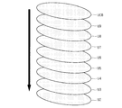
- FIG. 12 is a diagram schematically showing a process of sequentially laminating and joining a plurality of sheets U2 to U9 and UCB.
- a sheet shape is formed such that the chips of the sheets U2 to U5 are stacked immediately above each other.
- the alignment is performed as it is.
- the amount of deviation that is, the eccentricity accuracy of the optical axes of the three lens portions 41, 51, 81 is within 5 ⁇ m. Is desirable.
- an imaging sensor holder sheet U2 and an infrared cut filter sheet U3 are set in a known aligner device, and alignment using a previously formed alignment mark is performed.
- a so-called epoxy resin adhesive or ultraviolet curing adhesive is applied in advance to the surface (joint surface) to which the imaging sensor holder sheet U2 and the infrared cut filter sheet U3 are joined. Sheets U2 and U3 are joined.
- a method may be used in which the joining surfaces are activated by irradiating the joining surfaces with O 2 plasma and both sheets U2 and U3 are directly joined.
- the first lens sheet U4 is bonded onto the infrared cut filter sheet U3 and the second lens sheet U5 is bonded onto the first lens sheet U4 by the same alignment and bonding method as described above.
- each of the sheets U2 to U5 is provided with through holes Ca2 to Ca5 and Cb2 to Cb5 penetrating through predetermined positions in the respective chips.
- the four sheets U2 to U5 are stacked vertically by stacking and bonding.
- a through hole in which the through holes Ca2 to Ca5 are integrally connected and a through hole in which the through holes Cb2 to Cb5 are integrally connected are formed.
- a shadow mask or the like is applied to the two through holes of each chip of the four sheets U2 to U5, and a metal such as electroless plating (for example, gold) is plated.
- a metal such as electroless plating (for example, gold) is plated.
- the actuator sheet U6, the parallel unsprung sheet U7, the third lens sheet U8, and the parallel unsprung sheet U9 are arranged in this order on the top surface of the laminate formed by laminating the four sheets U2 to U5. Laminated and joined in order from the bottom.
- the alignment and joining method is the same as the method related to the above-described sheets U2 and U3. At this time, the chips of the sheets U2 to U9 are stacked immediately above each other.
- the lens portion 81 of the third lens sheet U8 is supported by the actuator portions 61a and 61b of the actuator sheet U6 via the elastic portion 71 of the parallel unsprung sheet U7. Further, the sheets U7 to U9 are stacked and joined, whereby the lens holding portion 83 is sandwiched by the elastic portions 71 and 91 from the upper and lower surfaces, and the lens portion 81 is supported by the elastic portions 71 and 91.
- connecting portions 84a and 84b for connecting the frame portion F8 and the lens portion 81 via the lens holding portion 83 are so-called femtosecond lasers or the like. The frame portion F8 and the lens portion 81 are separated.
- the lens unit 81 is movable after the lens unit 81 of each chip is supported by the elastic units 71 and 91. For this reason, the lens unit 81 and the actuator units 61a and 61b can be accurately aligned. That is, for example, it is possible to prevent the eccentricity of the optical axis of the lens portion in each optical unit (described later).
- the protective sheet UCB is aligned and joined to the upper surface of the parallel spring upper sheet U9 by the same method as described above.
- a member (laminated member) in which nine sheets U2 to U9 and UCB are laminated is formed.
- ⁇ Dicing (Process C): An optical system unit (optical unit) in which the laminated member formed by laminating the nine sheets U2 to U9 and UCB is separated for each chip by the dicing apparatus, and the nine layers 20 to 90 and CB are laminated. Many are generated.
- ⁇ Inspection of eccentricity of optical axis (process D): With respect to a large number of optical units generated by the dicing, a deviation amount of the optical axes (that is, eccentricity) of the three lens portions 41, 51, 81 is determined within a predetermined allowable range (for example, within 5 ⁇ m) by a lens eccentricity measuring machine. ) Is inspected whether it is in.
- the reason for the inspection of the eccentricity of the optical axis will be briefly described.
- the imaging element layer 10 is the most expensive among the components constituting the camera module 400.
- the camera module 400 in which the eccentricity of the optical axis deviates from the predetermined allowable value range is treated as a defective product.
- defective products and non-defective products are selected at the stage of the optical unit, and the imaging element layer 10 is attached only to non-defective products, thereby reducing the manufacturing cost of the camera module 400 and the waste of resources. Is possible.
- the chip of the imaging element layer 10 is a so-called epoxy resin system on the lower surface (specifically, the back surface of the imaging sensor holder layer 20) of each optical unit determined to be a non-defective product by inspection of the eccentricity of the optical axis.
- the camera module 400 is completed by being attached by bonding using an adhesive or an ultraviolet curable adhesive.
- the camera module 400 is formed by laminating the plurality of layers 10 to 90 and the CB including the imaging element layer 10, the third lens layer 80, and the actuator layer 60. For this reason, both high functionality and high accuracy in a compact imaging device are compatible.
- adjacent layers included in the plurality of layers 10 to 90 and CB constituting the camera module 400 are joined at the outer peripheral portion F1 and the frame portions F4 to F9. For this reason, the imaging element unit 11, the lens units 41, 51, 81, and the actuator units 61a, 61b are easily sealed.
- each optical unit is To be separated.
- achieves several functions can be combined easily and accurately. That is, it is possible to achieve both high functionality and high accuracy in a small imaging device.
- the imaging element layer 10 is attached. For this reason, it is possible to reduce wasteful disposal of the image sensor unit 11 due to a defect in the optical unit. That is, it is possible to reduce the manufacturing cost of the imaging apparatus and the wasteful use of resources.
- the camera module 400 is formed by laminating 10 layers, but the present invention is not limited to this.
- the lens portion 81 having the lens power and the frame portion F8 are made of a thin plate-like elastic member made of the same material as the lens portion 81, so that the lens portion 81 is at least two places around the lens portion 81.
- the parallel spring lower layer 70 and the parallel spring upper layer 90 may be omitted. That is, for the third lens layer 80, a structure in which the frame portion F8 and the lens portion 81 are connected by at least three elastic members from different directions around the lens portion 81 may be employed.
- the place where three or more elastic members are provided is a place where the frame part F8 can support the lens part 81 without deviation, such as substantially equidistant positions along the circumferential direction around the optical axis of the lens part 81. It is desirable that
- the other layers 70 and 90 having the elastic portions 71 and 91 for holding the lens portion 81 are not required, so that the assembly accuracy is improved by simplifying the structure of the camera module 400. Further, the camera module 400 can be reduced in thickness and size.
- the first and second lens layers 40 and 50 can be omitted as appropriate. Therefore, from the viewpoint of accurately supporting the lens unit 81 with the actuator unit, the camera module 400 includes a plurality of lenses including at least the lens layer 80 having the moving lens unit 81 and the actuator layer 60 moving the lens unit 81. These layers may be formed by being laminated.
- the parallel spring lower layer 70 and the parallel spring upper layer 90 described above are omitted, it is not necessary to cut the coupling portions 84a and 84b with a laser or the like as compared with the above-described embodiment.
- the camera module can be assembled with high accuracy while suppressing the occurrence of eccentricity.
- the eccentricity of the optical axis of the optical unit is inspected after dicing and the imaging element layer 10 is attached to a good optical unit.
- the present invention is not limited to this.
- the imaging element layer 10 shown in FIG. 3A is arranged on a predetermined substrate (for example, a silicon substrate) (here, Then, a large number of sheets (imaging device sheets) are formed in a matrix-like predetermined arrangement), and when the nine sheets U2 to U9 and UCB are laminated, the imaging device sheets are also aligned and stacked.
- a large number of camera modules 400 may be completed by dicing after bonding.
- the through holes formed by integrally connecting the through holes Ca2 to Ca5 and the through holes Cb2 to Cb5 are integrally connected.
- the wiring is formed by plating a metal with respect to the formed through hole, the present invention is not limited to this.
- the wirings CTa and CTb may be formed by plating a metal with respect to the through holes formed and the through holes formed by integrally connecting the through holes Cb1 to Cb5, Cb61, and Cb62.
- the five sheets U2 to U6 are filled with a conductive material, for example, by plating a metal in the through holes Ca2 to Ca5, Ca61, Ca62, Cb2 to Cb5, Cb61, and Cb62 for each sheet.
- the wirings CTa and CTb may be formed at the time of stacking of U6.
- the voltage supply wirings CTa and CTb penetrating through five of the ten layers constituting the camera module 400 are provided.
- the present invention is not limited to this.
- the image sensor layer 10 is not provided with a penetrating wiring, and a voltage supply wiring is appropriately provided in the image sensor layer 10 in the same manner as various signal wirings arranged in the image sensor layer 10.
- the first and second lens layers 40 and 50 can be appropriately omitted depending on the design of the optical system. Therefore, from the viewpoint of easily and accurately forming a wiring portion for applying an electric field to the actuator portions 61a and 61b, among the plurality of layers constituting the camera module 400, the imaging element layer 10 and the actuator layer 60 It is only necessary to provide a wiring that passes through one or more layers disposed between the actuator layers 60 and applies an electric field to the actuator layer 60.
- the base layer 601 is provided with the through holes Ca61 and Cb61 and then filled with the conductive material.
- the present invention is not limited to this.
- ion doping is applied to the silicon thin plate used as the base layer 601 material. By applying, a conductive region may be formed.
- the through holes Ca2 to Ca5 and Cb2 to Cb5 penetrating the plurality of sheets U2 to U5 are formed for each sheet.
- the present invention is not limited to this.
- a so-called femtosecond laser, excimer laser, or ionic etching method is used to form through-holes that penetrate four sheets having a size of about several tens of ⁇ m. May be.
- the voltage is applied to the actuator portions 61a and 61b by the wirings CTa and CTb penetrating a plurality of layers, but the present invention is not limited to this.
- the terminal portion functions as a terminal for electrically connecting a wiring for applying an electric field to the actuator portions 61 a and 61 b from the outside of the actuator layer 60.
- the shape memory alloy is used as the actuator element.
- the present invention is not limited to this.
- an inorganic piezoelectric material such as PZT (lead zirconate titanate) is used.
- a piezoelectric element such as an organic piezoelectric body such as polyvinylidene fluoride (PVDF) may be used.
- PVDF polyvinylidene fluoride
- the actuator portions 61a and 61b are formed on the base layer 601 by forming a thin film of the actuator element via the insulating layer 602 and the insulating films 614a and 614b.
- a thin film of the actuator element via the insulating layer 602 and the insulating films 614a and 614b.
- An actuator part may be formed by forming a metal thin film.
- a mode in which the base layer is made of silicon (Si) and the metal thin film is made of aluminum (Al) is conceivable.
- the elastic portions 71 and 91 are fixed to the two portions of the frame portions F7 and F9, respectively.
- the present invention is not limited to this, and various configurations may be adopted.
- the elastic units 71 and 91 are preferably fixed at two or more locations of the frame units F7 and F9, respectively. .
- both ends of the elastic portion 71 are fixed at a total of two locations of the frame portion F7, and both ends of the elastic portion 91 are fixed at a total of two locations of the frame portion F9.
- each of the elastic portions 71 and 91 is divided into two at the center portion, and one end of the elastic portion 71 divided into two and the other end are fixed to the frame portion F7, respectively, and fixed in two places in total.
- a configuration is also conceivable in which one end of the elastic part 91 divided into two and the other end are fixed to the frame part F9 to be fixed in two places in total.
Abstract
Description
図2は、カメラモジュール400の構成例を模式的に示す分解斜視図である。 <Configuration of camera module>
FIG. 2 is an exploded perspective view schematically showing a configuration example of the
図3および図4は、撮像素子層10、撮像センサホルダ層20、赤外カットフィルタ層30、第1レンズ層40、第2レンズ層50、アクチュエータ層60、平行バネ下層70、第3レンズ層80、平行バネ上層90、および保護層CBの構成例をそれぞれ示す平面図である。 <Configuration of each layer>
3 and 4 show the
図3(a)で示すように、撮像素子層10は、例えば、COMSセンサまたはCCDセンサなどで形成される撮像素子部11、その周辺回路、および撮像素子部11を囲む外周部F1を備えるチップである。なお、ここでは図示を省略しているが、撮像素子層10の裏面(-Z側の面)には、撮像素子部11に対する信号の付与、および撮像素子部11からの信号の読み出しを行うための配線を接続するための各種端子が設けられる。 ○ Image sensor layer 10:
As shown in FIG. 3A, the
図3(b)で示すように、撮像センサホルダ層20は、例えば、樹脂などの素材によって形成され、接合によって取り付けられる撮像素子層10を保持するチップである。具体的には、撮像センサホルダ層20の略中央には、断面が略正方形の開口21がZ方向に沿って設けられ、該開口21の断面は+Z側に行くに従って小さくなる。なお、図3(b)の破線で描かれた四角形は、-Z側の面における開口21の外縁を示す。 ○ Imaging sensor holder layer 20:
As shown in FIG. 3B, the imaging
図3(c)で示すように、赤外カットフィルタ層30は、透明基板上に屈折率の異なる透明薄膜が多層化されて構成された赤外線をカットするフィルタのチップである。具体的には、赤外カットフィルタ層30は、例えば、ガラスまたは透明樹脂で構成される基板の上面に屈折率の異なる多数の透明薄膜をスパッタリングなどで形成したもので、薄膜の厚みおよび屈折率の組合せにより、透過する光の波長帯が制御される。例えば、赤外カットフィルタ層30としては、600nm以上の波長帯の光を遮断するものが好ましい。 ○ Infrared cut filter layer 30:
As shown in FIG. 3 (c), the infrared
図3(d)で示すように、第1レンズ層40は、正のレンズパワーを有する光学レンズからなるレンズ部41と、該レンズ部41を囲み且つ該第1レンズ層40の外周部を構成する枠部F4とが同一の素材で一体成型されて形成されたチップである。そして、第1レンズ層40を構成する素材としては、フェノール系の樹脂やアクリル系の樹脂、あるいはガラスなどが挙げられる。なお、レンズ部41は、第1~3レンズ層40,50,80による焦点が撮像素子部11に対応したものとなるように光を屈折させる光学レンズとなっている。 ○ First lens layer 40:
As shown in FIG. 3D, the
図3(e)で示すように、第2レンズ層50は、負のレンズパワーを有する光学レンズからなるレンズ部51と、該レンズ部51を囲み且つ該第2レンズ層50の外周部を構成する枠部F5とが同一の素材で一体成型されて形成されたチップである。そして、第2レンズ層50を構成する素材としては、第1レンズ層40と同様に、フェノール系の樹脂やアクリル系の樹脂、あるいはガラスなどが挙げられる。なお、レンズ部51は、レンズ部41と同様に、第1~3レンズ層40,50,80による焦点が撮像素子部11に対応したものとなるように光を屈折させる光学レンズとなっている。 ○ Second lens layer 50:
As shown in FIG. 3E, the
図3(f)で示すように、アクチュエータ層60は、撮像素子層10の撮像面側に配置されるとともに、第3レンズ層80のレンズ部81を移動させる薄板状のアクチュエータ部61a,61bを備えるチップである。このアクチュエータ層60は、シリコン(Si)製の基板上に変位用の素子(アクチュエータ素子)が薄膜状に形成される。本実施形態では、アクチュエータ素子として、形状記憶合金(SMA)を用いるものとする。 ○ Actuator layer 60:
As shown in FIG. 3F, the
図4(a)で示すように、平行バネ下層70は、りん青銅などの金属材料で構成され、枠部F7と、弾性部71とを有するチップであり、バネ機構を形成する層(弾性層)となっている。 ○ Parallel spring lower layer 70:
As shown in FIG. 4A, the parallel spring
図4(b)で示すように、第3レンズ層80は、枠部F8と、レンズ部81と、レンズ保持部83とを有するチップである。この第3レンズ層80を構成する素材としては、第1および第2レンズ層40,50と同様に、フェノール系の樹脂やアクリル系の樹脂、あるいはガラスなどが挙げられる。 ○ Third lens layer 80:
As shown in FIG. 4B, the
図4(c)で示すように、平行バネ上層90は、平行バネ下層70と同様な構成を有し、りん青銅などの金属材料で構成され、枠部F9と、弾性部91とを有するチップであり、バネ機構を形成する層(弾性層)となっている。 ○ Parallel spring upper layer 90:
As shown in FIG. 4C, the parallel spring
図4(d)で示すように、保護層CBは、盤面が略正方形の板状の透明部材であり、例えば、樹脂やガラスなどによって構成される。そして、保護層CBの外周部の-Z側の面が隣接する平行バネ上層90(具体的には、枠部F9)と接合される。保護層CBの外周部は、例えば、外周に沿って凸形状を持つ構造にして、凸形状の上端面で接合するようにしても良い。 ○ Protective layer CB:
As shown in FIG. 4D, the protective layer CB is a plate-shaped transparent member having a substantially square board surface, and is made of, for example, resin or glass. The surface on the −Z side of the outer peripheral portion of the protective layer CB is joined to the adjacent parallel spring upper layer 90 (specifically, the frame portion F9). For example, the outer peripheral portion of the protective layer CB may be structured to have a convex shape along the outer periphery, and may be joined at the upper end surface of the convex shape.
図7は、カメラモジュール400の構造を示す図である。詳細には、図7(a)は、カメラモジュール400を保護層CB側(上方)から見た平面図であり、図7(b)は、図7(a)の切断面線7A-7Aから見た断面模式図である。なお、図7(b)では、切断面よりも-Y側に位置している貫通孔Ca1~Ca5,Ca61,Ca62が繋がって形成される1つの貫通孔Cva、および貫通孔Cb1~Cb5,Cb61,Cb62が繋がって形成される1つの貫通孔Cvbの位置関係が分かるように、それぞれが破線で示されている。 <Complete structure of camera module>
FIG. 7 is a diagram illustrating the structure of the
図8は、第3レンズ層80に含まれるレンズ部81の駆動態様を説明するための図である。図8では、レンズ部81と弾性部71,91の状態を側方から見た模式図が示されている。なお、実際にはレンズ保持部83を弾性部71,91が挟持しているが、図8では、説明の簡略化のために、弾性部71,91がレンズ部81を点Pu,Pdで保持しているように示されている。また、図8(a)では、弾性部71,91が変形していない状態(初期状態)が示され、図8(b)では、弾性部71,91が変形している状態(変形状態)が示されている。 <Mode of driving the lens unit>
FIG. 8 is a diagram for explaining a driving mode of the
図9は、カメラモジュール400の製造工程の手順を例示するフローチャートである。図9で示すように、(工程A)複数のシートの準備(ステップS1)、(工程B)複数のシートの接合(ステップS2)、(工程C)ダイシング(ステップS3)、(工程D)光軸の偏芯の検査(ステップS4)、および(工程E)撮像素子層の結合(ステップS5)が順次に行われることで、カメラモジュール400が製造される。以下、各工程について説明する。 <Camera module manufacturing process>
FIG. 9 is a flowchart illustrating the procedure of the manufacturing process of the
図10および図11は、準備する10枚のシートU2~U9,UCBの構成例を示す平面図である。ここでは、各シートU2~U9,UCBが、円盤状である例を示して説明する。 ○ Preparation of multiple sheets (Process A):
FIG. 10 and FIG. 11 are plan views showing a configuration example of ten sheets U2 to U9, UCB to be prepared. Here, description will be given by showing an example in which each of the sheets U2 to U9, UCB has a disk shape.
図12は、複数のシートU2~U9,UCBを順次に積層させて接合する工程を模式的に示す図である。 ○ Joining multiple sheets (process B):
FIG. 12 is a diagram schematically showing a process of sequentially laminating and joining a plurality of sheets U2 to U9 and UCB.
9つのシートU2~U9,UCBが積層された形成された積層部材が、ダイシング装置によってチップ毎に切り離されて、9つの層20~90,CBが積層された光学系のユニット(光学ユニット)が多数生成される。 ○ Dicing (Process C):
An optical system unit (optical unit) in which the laminated member formed by laminating the nine sheets U2 to U9 and UCB is separated for each chip by the dicing apparatus, and the nine
上記ダイシングによって生成された多数の光学ユニットについて、レンズ偏芯測定機によって、3つのレンズ部41,51,81の光軸のズレ量(すなわち偏芯)が所定の許容値域範囲(例えば、5μm以内)に入っているのか否か検査される。 ○ Inspection of eccentricity of optical axis (process D):
With respect to a large number of optical units generated by the dicing, a deviation amount of the optical axes (that is, eccentricity) of the three
光軸の偏芯の検査によって良品であると判別された各光学ユニットの下面(具体的には、撮像センサホルダ層20の裏面)に対して、撮像素子層10のチップが、いわゆるエポキシ樹脂系の接着剤、または紫外線硬化接着剤を用いた接合によって取り付けられて、カメラモジュール400が完成される。 ○ Bonding of imaging element layer (process E):
The chip of the
本発明は上述の実施の形態に限定されるものではなく、本発明の要旨を逸脱しない範囲において種々の変更、改良等が可能である。 <Modification>
The present invention is not limited to the above-described embodiments, and various changes and improvements can be made without departing from the scope of the present invention.
11 撮像素子部
20 撮像センサホルダ層
30 赤外カットフィルタ層
40 第1レンズ層
41,51,81 レンズ部
50 第2レンズ層
60 アクチュエータ層
61a,61b アクチュエータ部
70 平行バネ下層
71,91 弾性部
80 第3レンズ層
83 レンズ保持部
84a,84b 連結部
90 平行バネ上層
100 携帯電話機
400 カメラモジュール
Ca1~Ca5,Ca61,Ca62,Cb1~Cb5,Cb61,Cb62,Cva,Cvb 貫通孔
CB 保護層
CTa,CTb 配線
F1 外周部
F4~F9 枠部
U2 撮像センサホルダシート
U3 赤外カットフィルタシート
U4 第1レンズシート
U5 第2レンズシート
U6 アクチュエータシート
U7 平行バネ下シート
U8 第3レンズシート
U9 平行バネ上シート
UCB 保護層シート DESCRIPTION OF
Claims (16)
- 撮像素子部を有する撮像素子層と、
前記撮像素子部からの距離が変更可能なレンズ部を有し、且つ前記撮像素子部のうちの被写体からの光を受光する撮像面側に配置されるレンズ層と、
前記レンズ部を移動させるアクチュエータ部を有し、且つ前記撮像素子部の前記撮像面側に配置されるアクチュエータ層と、
を含む複数の層が積層されて形成されることを特徴とする撮像装置。 An image sensor layer having an image sensor section;
A lens layer that has a lens unit that can change the distance from the image sensor unit, and that is disposed on the imaging surface side that receives light from the subject in the image sensor unit; and
An actuator layer that moves the lens unit, and is disposed on the imaging surface side of the imaging element unit; and
An image pickup apparatus comprising a plurality of layers including a stacked layer. - 請求項1に記載の撮像装置であって、
前記撮像素子層が、
前記撮像素子部を囲む外周部を有し、
前記レンズ層が、
前記レンズ部を囲む第1枠部を有し、
前記アクチュエータ層が、
前記アクチュエータ部の一端が固設され、且つ前記アクチュエータ部を囲む第2枠部を有し、
前記外周部が、
前記複数の層のうちの前記撮像素子層に隣接する層に接合され、
前記第1枠部が、
前記複数の層のうちの前記レンズ層に隣接する層に接合され、
前記第2枠部が、
前記複数の層のうちの前記アクチュエータ層に隣接する層に接合されることを特徴とする撮像装置。 The imaging apparatus according to claim 1,
The imaging element layer is
An outer peripheral portion surrounding the imaging element portion;
The lens layer is
A first frame portion surrounding the lens portion;
The actuator layer is
One end of the actuator part is fixed, and has a second frame part surrounding the actuator part,
The outer periphery is
Bonded to a layer adjacent to the imaging element layer of the plurality of layers,
The first frame portion is
Bonded to a layer adjacent to the lens layer of the plurality of layers,
The second frame portion is
An image pickup apparatus bonded to a layer adjacent to the actuator layer among the plurality of layers. - 請求項2に記載の撮像装置であって、
前記複数の層が、
前記第1枠部に対して一方向から接合される第3枠部と、該第3枠部の少なくとも2カ所において固設される第1弾性部とを有する第1弾性層と、
前記第1枠部に対して前記一方向とは反対方向から接合される第4枠部と、該第4枠部の少なくとも2カ所において固設される第2弾性部とを有する第2弾性層と、
を含み、
前記レンズ層が、
前記レンズ部を保持し、且つ前記第1弾性部と前記第2弾性部とで挟持されるレンズ保持部を有することを特徴とする撮像装置。 The imaging apparatus according to claim 2,
The plurality of layers are
A first elastic layer having a third frame portion joined from one direction to the first frame portion, and first elastic portions fixed at least at two locations of the third frame portion;
A second elastic layer having a fourth frame part joined to the first frame part from a direction opposite to the one direction, and a second elastic part fixed at at least two positions of the fourth frame part. When,
Including
The lens layer is
An imaging apparatus comprising: a lens holding portion that holds the lens portion and is sandwiched between the first elastic portion and the second elastic portion. - 請求項2に記載の撮像装置であって、
前記レンズ層が、
前記第1枠部と前記レンズ部とを連結する少なくとも3つの弾性部を有することを特徴とする撮像装置。 The imaging apparatus according to claim 2,
The lens layer is
An image pickup apparatus comprising at least three elastic portions that connect the first frame portion and the lens portion. - 請求項1に記載の撮像装置であって、
前記複数の層のうちの前記撮像素子層と前記アクチュエータ層との間に配置される1以上の層を貫通し、且つ前記アクチュエータ層に電界を付与する配線部、
を更に備えることを特徴とする撮像装置。 The imaging apparatus according to claim 1,
A wiring portion penetrating one or more layers disposed between the imaging element layer and the actuator layer of the plurality of layers and applying an electric field to the actuator layer;
An image pickup apparatus further comprising: - 請求項1に記載の撮像装置であって、
前記アクチュエータ層が、
外縁部において、前記アクチュエータ部に対して電気的に接続され、且つ前記アクチュエータ部に電界を付与するための配線を接続する端子部を更に有することを特徴とする撮像装置。 The imaging apparatus according to claim 1,
The actuator layer is
An image pickup apparatus further comprising a terminal portion that is electrically connected to the actuator portion at an outer edge portion and connects a wiring for applying an electric field to the actuator portion. - 請求項1に記載の撮像装置であって、
前記複数の層に含まれる相互に隣接する2層の間に、該2層を接合する樹脂が介在することを特徴とする撮像装置。 The imaging apparatus according to claim 1,
An imaging apparatus, wherein a resin for joining the two layers is interposed between two adjacent layers included in the plurality of layers. - 請求項1に記載の撮像装置であって、
前記アクチュエータ部が、
基板と、該基板上に形成される形状記憶合金の薄膜とを含むことを特徴とする撮像装置。 The imaging apparatus according to claim 1,
The actuator part is
An imaging apparatus comprising: a substrate; and a shape memory alloy thin film formed on the substrate. - 請求項1に記載の撮像装置であって、
前記アクチュエータ部が、
基板と、該基板上に形成される圧電素子の薄膜とを含むことを特徴とする撮像装置。 The imaging apparatus according to claim 1,
The actuator part is
An imaging device comprising: a substrate; and a piezoelectric element thin film formed on the substrate. - 請求項1に記載の撮像装置であって、
前記アクチュエータ部が、
基板と、該基板上に形成され且つ該基板とは線膨張係数が異なる金属薄膜とを含むことを特徴とする撮像装置。 The imaging apparatus according to claim 1,
The actuator part is
An imaging apparatus comprising: a substrate; and a metal thin film formed on the substrate and having a linear expansion coefficient different from that of the substrate. - レンズ部をそれぞれ有する複数のチップが所定配列で形成される第1シートと、アクチュエータ部をそれぞれ有する複数のチップが前記所定配列で形成される第2シートとを含む複数枚のシートを準備するシート準備工程と、
各前記レンズ部が各前記アクチュエータ部によって支持されるように前記複数枚のシートを積層させつつ結合することで積層部材を形成する積層部材形成工程と、
前記積層部材を前記チップ毎に切り離すことで、前記レンズ部と該レンズ部を移動可能に支持する前記アクチュエータ部とをそれぞれ有する複数のユニットを生成するユニット生成工程と、
を備えることを特徴とする撮像装置の製造方法。 A sheet for preparing a plurality of sheets including a first sheet in which a plurality of chips each having a lens portion are formed in a predetermined arrangement and a second sheet in which a plurality of chips each having an actuator portion are formed in the predetermined arrangement A preparation process;
A laminated member forming step of forming a laminated member by laminating and bonding the plurality of sheets so that each lens unit is supported by each actuator unit;
A unit generation step of generating a plurality of units each having the lens unit and the actuator unit that movably supports the lens unit by separating the laminated member for each chip,
An image pickup apparatus manufacturing method comprising: - 請求項11に記載の撮像装置の製造方法であって、
前記複数枚のシートが、
撮像素子部をそれぞれ有する複数のチップが前記所定配列で形成された第3シートを含むことを特徴とする撮像装置の製造方法。 It is a manufacturing method of the imaging device according to claim 11,
The plurality of sheets are
A manufacturing method of an imaging apparatus, wherein a plurality of chips each having an imaging element unit includes a third sheet formed in the predetermined array. - 請求項11に記載の撮像装置の製造方法であって、
前記ユニット生成工程によって生成された各前記ユニットに対して、撮像素子部を有する撮像素子層を取り付ける撮像素子取付工程、
を更に備えることを特徴とする撮像装置の製造方法。 It is a manufacturing method of the imaging device according to claim 11,
An image sensor attaching step for attaching an image sensor layer having an image sensor portion to each unit generated by the unit generating step,
An image pickup apparatus manufacturing method, further comprising: - 請求項12に記載の撮像装置の製造方法であって、
前記複数枚のシートが、
所定部材をそれぞれ有し、且つ各前記撮像素子部の取り付け先となる複数のチップが前記所定配列で形成される第4シートを含み、
前記複数枚のシートのうち、前記第4シートを含み、且つ前記積層部材形成工程において前記第2シートよりも前記第4シート側に積層される1枚以上のシートが、
各チップの所定位置を貫通する孔部をそれぞれ有し、
更に、前記撮像装置の製造方法が、
前記積層部材形成工程の途中または該積層部材形成工程の後において、各前記孔部に対して金属をめっきすることで、前記アクチュエータ部に電界を付与する配線部を形成する配線形成工程、
を備えることを特徴とする撮像装置の製造方法。 It is a manufacturing method of the imaging device according to claim 12,
The plurality of sheets are
Each of the plurality of chips each having a predetermined member and serving as an attachment destination of each of the imaging element units includes a fourth sheet formed in the predetermined arrangement,
Among the plurality of sheets, one or more sheets including the fourth sheet and laminated on the fourth sheet side with respect to the second sheet in the laminated member forming step,
Each has a hole penetrating a predetermined position of each chip,
Furthermore, the manufacturing method of the imaging device includes:
In the middle of the laminated member forming step or after the laminated member forming step, a wiring forming step of forming a wiring portion for applying an electric field to the actuator portion by plating a metal on each of the holes,
An image pickup apparatus manufacturing method comprising: - 請求項12に記載の撮像装置の製造方法であって、
前記第1シートの各チップが、
前記レンズ部を囲む第1枠部と、該第1枠部と前記レンズ部とを連結する連結部とを有し、
前記複数枚のシートが、
前記第1枠部に対して一方向から接合するための第2枠部と、該第2枠部の少なくとも2カ所において固設される第1弾性部とをそれぞれ有する複数のチップが前記所定配列で形成された第5シートと、
前記第1枠部に対して前記一方向とは反対方向から接合するための第3枠部と、該第3枠部の少なくとも2カ所において固設される第2弾性部とをそれぞれ有する複数のチップが前記所定配列で形成された第6シートと、
を含み、
前記積層部材形成工程において、前記レンズ部が前記第1弾性部と前記第2弾性部とによって支持されるように前記第1、第5、および第6シートを積層して結合した後に、各チップにおいて、前記連結部を切断することで、前記第1枠部と前記レンズ部とを分離することを特徴とする撮像装置の製造方法。 It is a manufacturing method of the imaging device according to claim 12,
Each chip of the first sheet is
A first frame part surrounding the lens part; and a connecting part for connecting the first frame part and the lens part;
The plurality of sheets are
A plurality of chips each having a second frame portion for joining to the first frame portion from one direction and first elastic portions fixed at least at two locations of the second frame portion are arranged in the predetermined array. A fifth sheet formed by:
A plurality of frames each having a third frame portion for joining to the first frame portion from a direction opposite to the one direction, and a second elastic portion fixed at at least two locations of the third frame portion. A sixth sheet in which the chips are formed in the predetermined arrangement;
Including
In the laminated member forming step, each chip is formed after the first, fifth, and sixth sheets are laminated and bonded so that the lens portion is supported by the first elastic portion and the second elastic portion. The method for manufacturing an imaging device according to claim 1, wherein the first frame portion and the lens portion are separated by cutting the connecting portion. - 請求項11に記載の撮像装置の製造方法であって、
前記積層部材形成工程において、
前記複数枚のシートに含まれる隣接する2枚のシートの間を樹脂によって結合することを特徴とする撮像装置の製造方法。 It is a manufacturing method of the imaging device according to claim 11,
In the laminated member forming step,
A method for manufacturing an image pickup apparatus, comprising: bonding two adjacent sheets included in the plurality of sheets with a resin.
Priority Applications (5)
| Application Number | Priority Date | Filing Date | Title |
|---|---|---|---|
| EP09727470A EP2259572A4 (en) | 2008-04-03 | 2009-04-01 | Imaging device and imaging device manufacturing method |
| JP2010505977A JP5223917B2 (en) | 2008-04-03 | 2009-04-01 | Imaging device and manufacturing method of imaging device |
| US12/933,076 US8384812B2 (en) | 2008-04-03 | 2009-04-01 | Imaging device formed by lamination of a plurality of layers |
| CN2009801095294A CN101978683B (en) | 2008-04-03 | 2009-04-01 | Imaging device and imaging device manufacturing method |
| US13/743,548 US8715444B2 (en) | 2008-04-03 | 2013-01-17 | Imaging device and imaging device manufacturing method |
Applications Claiming Priority (2)
| Application Number | Priority Date | Filing Date | Title |
|---|---|---|---|
| JP2008097228 | 2008-04-03 | ||
| JP2008-097228 | 2008-04-03 |
Publications (1)
| Publication Number | Publication Date |
|---|---|
| WO2009123266A1 true WO2009123266A1 (en) | 2009-10-08 |
Family
ID=41135633
Family Applications (1)
| Application Number | Title | Priority Date | Filing Date |
|---|---|---|---|
| PCT/JP2009/056823 WO2009123266A1 (en) | 2008-04-03 | 2009-04-01 | Imaging device and imaging device manufacturing method |
Country Status (6)
| Country | Link |
|---|---|
| US (2) | US8384812B2 (en) |
| EP (1) | EP2259572A4 (en) |
| JP (1) | JP5223917B2 (en) |
| KR (1) | KR20100129751A (en) |
| CN (2) | CN103336349A (en) |
| WO (1) | WO2009123266A1 (en) |
Cited By (5)
| Publication number | Priority date | Publication date | Assignee | Title |
|---|---|---|---|---|
| JP2011083847A (en) * | 2009-10-14 | 2011-04-28 | Konica Minolta Holdings Inc | Method for manufacturing actuator, actuator, and imaging device |
| JP2011172174A (en) * | 2010-02-22 | 2011-09-01 | Ricoh Co Ltd | Imaging apparatus, distance image capturing device, and manufacturing method thereof |
| WO2012058955A1 (en) * | 2010-11-02 | 2012-05-10 | Hong Kong Applied Science And Technology Research Institute Co. Ltd. | Compact imaging apparatus and method for manufacturing same |
| US8384812B2 (en) | 2008-04-03 | 2013-02-26 | Konica Minolta Holdings, Inc. | Imaging device formed by lamination of a plurality of layers |
| WO2018029739A1 (en) * | 2016-08-08 | 2018-02-15 | エスゼット ディージェイアイ テクノロジー カンパニー リミテッド | Mobile entity and method for manufacturing imaging device |
Families Citing this family (11)
| Publication number | Priority date | Publication date | Assignee | Title |
|---|---|---|---|---|
| US20070170528A1 (en) | 2006-01-20 | 2007-07-26 | Aaron Partridge | Wafer encapsulated microelectromechanical structure and method of manufacturing same |
| US8638369B2 (en) * | 2010-12-09 | 2014-01-28 | Apple Inc. | Back panel for a portable electronic device with different camera lens options |
| JP2013034046A (en) * | 2011-08-01 | 2013-02-14 | Sony Corp | Camera module, manufacturing apparatus, and manufacturing method |
| JP5980941B2 (en) * | 2012-10-12 | 2016-08-31 | シャープ株式会社 | Camera module and electronic equipment |
| JP2017032798A (en) * | 2015-07-31 | 2017-02-09 | ソニーセミコンダクタソリューションズ株式会社 | Substrate with lens, laminated lens structure, camera module, and apparatus and method manufacturing |
| US11092732B2 (en) * | 2015-12-18 | 2021-08-17 | Harman International Industries, Incorporates | Lens system and method |
| CN111913267B (en) * | 2016-04-01 | 2022-12-27 | 台湾东电化股份有限公司 | Lens driving mechanism |
| TWI618949B (en) * | 2016-04-01 | 2018-03-21 | 台灣東電化股份有限公司 | Lens driving mechanism and control method thereof |
| CN110087870B (en) * | 2017-01-26 | 2022-03-18 | 索尼半导体解决方案公司 | Laminated lens structure, method of manufacturing the same, and electronic apparatus |
| JP6987518B2 (en) | 2017-01-26 | 2022-01-05 | ソニーセミコンダクタソリューションズ株式会社 | Laminated lens structure and its manufacturing method, as well as electronic devices |
| CN112399036B (en) * | 2019-08-15 | 2022-07-26 | 宁波舜宇光电信息有限公司 | Method for manufacturing optical filter, optical filter and camera module |
Citations (4)
| Publication number | Priority date | Publication date | Assignee | Title |
|---|---|---|---|---|
| JP2006330559A (en) * | 2005-05-30 | 2006-12-07 | Nec Tokin Corp | Camera module using lamination type piezoelectric actuator |
| JP2007012995A (en) | 2005-07-01 | 2007-01-18 | Toshiba Corp | Microminiature camera module and method of manufacturing same |
| JP2007139862A (en) * | 2005-11-15 | 2007-06-07 | Olympus Corp | Lens driving mechanism |
| JP2008048388A (en) * | 2006-07-21 | 2008-02-28 | Konica Minolta Opto Inc | Imaging unit and imaging apparatus |
Family Cites Families (23)
| Publication number | Priority date | Publication date | Assignee | Title |
|---|---|---|---|---|
| JPH10173306A (en) * | 1996-12-06 | 1998-06-26 | Olympus Optical Co Ltd | Manufacturing method of shape memory alloy thin-film actuator |
| US7092174B2 (en) * | 2001-05-18 | 2006-08-15 | Konica Corporation | Image pickup lens, image pickup apparatus and method for forming image pickup lens |
| JP2002357773A (en) * | 2001-06-04 | 2002-12-13 | Olympus Optical Co Ltd | Optical component and endoscope and endoscopic optical system using the same |
| US7872394B1 (en) * | 2001-12-13 | 2011-01-18 | Joseph E Ford | MEMS device with two axes comb drive actuators |
| JP2003289457A (en) * | 2002-01-22 | 2003-10-10 | Casio Comput Co Ltd | Image apparatus |
| EP1490615A1 (en) * | 2002-03-29 | 2004-12-29 | D2 In-Line Solutions, LLC | Rotary barrel gate valve |
| CN1220089C (en) * | 2002-06-27 | 2005-09-21 | 奥林巴斯株式会社 | Camera shooting lens unit and pick-up device and method for manufacturing same |
| WO2004027880A2 (en) | 2002-09-17 | 2004-04-01 | Koninklijke Philips Electronics N.V. | Camera device, method of manufacturing a camera device, wafer scale package |
| US7280290B2 (en) * | 2004-09-16 | 2007-10-09 | Sony Corporation | Movable lens mechanism |
| JP2006122338A (en) * | 2004-10-28 | 2006-05-18 | Aruze Corp | Game machine and program |
| JP2006246656A (en) * | 2005-03-04 | 2006-09-14 | Seiko Precision Inc | Actuator, focusing device, and image pickup unit |
| JP2008020812A (en) * | 2006-07-14 | 2008-01-31 | Konica Minolta Opto Inc | Lens driving mechanism and imaging apparatus using same |
| US8175449B2 (en) * | 2006-05-30 | 2012-05-08 | Konica Minolta Opto, Inc. | Driving device, driving mechanism, and image sensing apparatus |
| KR100809277B1 (en) * | 2006-07-05 | 2008-03-03 | 삼성전기주식회사 | Camer module having a array lens |
| US8138564B2 (en) | 2006-07-20 | 2012-03-20 | Konica Minolta Opto, Inc. | Image sensor unit and image sensor apparatus |
| KR20080043106A (en) * | 2006-11-13 | 2008-05-16 | 삼성전자주식회사 | Optical lens and manufacturing method thereof |
| JP2008130810A (en) * | 2006-11-21 | 2008-06-05 | Seiko Precision Inc | Actuator and method for manufacturing the same |
| KR101210116B1 (en) * | 2007-05-31 | 2012-12-07 | 아트피셜 머슬, 인코퍼레이션 | Optical systems employing compliant electroactive materials |
| KR101222990B1 (en) * | 2007-10-22 | 2013-01-18 | 엘지디스플레이 주식회사 | Liquid Crystal Lens Electrically driven and Stereoscopy Display Device |
| JP4435290B2 (en) * | 2007-11-05 | 2010-03-17 | パナソニック株式会社 | Lens holder driving device and imaging device using surface-driven polymer actuator |
| CN101493561B (en) * | 2008-01-21 | 2012-03-14 | 鸿富锦精密工业(深圳)有限公司 | Carbon nanotube driver, lens module using the carbon nanotube driver and camera module |
| CN103336349A (en) | 2008-04-03 | 2013-10-02 | 柯尼卡美能达株式会社 | Imaging device and imaging device manufacturing method |
| CN101990738A (en) * | 2008-04-08 | 2011-03-23 | 柯尼卡美能达控股株式会社 | Actuator array sheet |
-
2009
- 2009-04-01 CN CN2013102012140A patent/CN103336349A/en active Pending
- 2009-04-01 EP EP09727470A patent/EP2259572A4/en not_active Withdrawn
- 2009-04-01 KR KR1020107021705A patent/KR20100129751A/en not_active Application Discontinuation
- 2009-04-01 WO PCT/JP2009/056823 patent/WO2009123266A1/en active Application Filing
- 2009-04-01 JP JP2010505977A patent/JP5223917B2/en not_active Expired - Fee Related
- 2009-04-01 US US12/933,076 patent/US8384812B2/en not_active Expired - Fee Related
- 2009-04-01 CN CN2009801095294A patent/CN101978683B/en not_active Expired - Fee Related
-
2013
- 2013-01-17 US US13/743,548 patent/US8715444B2/en not_active Expired - Fee Related
Patent Citations (4)
| Publication number | Priority date | Publication date | Assignee | Title |
|---|---|---|---|---|
| JP2006330559A (en) * | 2005-05-30 | 2006-12-07 | Nec Tokin Corp | Camera module using lamination type piezoelectric actuator |
| JP2007012995A (en) | 2005-07-01 | 2007-01-18 | Toshiba Corp | Microminiature camera module and method of manufacturing same |
| JP2007139862A (en) * | 2005-11-15 | 2007-06-07 | Olympus Corp | Lens driving mechanism |
| JP2008048388A (en) * | 2006-07-21 | 2008-02-28 | Konica Minolta Opto Inc | Imaging unit and imaging apparatus |
Non-Patent Citations (1)
| Title |
|---|
| See also references of EP2259572A4 |
Cited By (9)
| Publication number | Priority date | Publication date | Assignee | Title |
|---|---|---|---|---|
| US8384812B2 (en) | 2008-04-03 | 2013-02-26 | Konica Minolta Holdings, Inc. | Imaging device formed by lamination of a plurality of layers |
| US8715444B2 (en) | 2008-04-03 | 2014-05-06 | Konica Minolta Holdings, Inc. | Imaging device and imaging device manufacturing method |
| JP2011083847A (en) * | 2009-10-14 | 2011-04-28 | Konica Minolta Holdings Inc | Method for manufacturing actuator, actuator, and imaging device |
| JP2011172174A (en) * | 2010-02-22 | 2011-09-01 | Ricoh Co Ltd | Imaging apparatus, distance image capturing device, and manufacturing method thereof |
| WO2012058955A1 (en) * | 2010-11-02 | 2012-05-10 | Hong Kong Applied Science And Technology Research Institute Co. Ltd. | Compact imaging apparatus and method for manufacturing same |
| WO2018029739A1 (en) * | 2016-08-08 | 2018-02-15 | エスゼット ディージェイアイ テクノロジー カンパニー リミテッド | Mobile entity and method for manufacturing imaging device |
| JPWO2018029739A1 (en) * | 2016-08-08 | 2019-06-27 | エスゼット ディージェイアイ テクノロジー カンパニー リミテッドSz Dji Technology Co.,Ltd | Mobile body and method of manufacturing imaging device |
| US10890829B2 (en) | 2016-08-08 | 2021-01-12 | SZ DJI Technology Co., Ltd. | Movable object and method for manufacturing photographing device |
| JP7009696B2 (en) | 2016-08-08 | 2022-01-26 | エスゼット ディージェイアイ テクノロジー カンパニー リミテッド | Mobile |
Also Published As
| Publication number | Publication date |
|---|---|
| JPWO2009123266A1 (en) | 2011-07-28 |
| KR20100129751A (en) | 2010-12-09 |
| CN101978683A (en) | 2011-02-16 |
| US8384812B2 (en) | 2013-02-26 |
| JP5223917B2 (en) | 2013-06-26 |
| US20130126083A1 (en) | 2013-05-23 |
| EP2259572A1 (en) | 2010-12-08 |
| CN101978683B (en) | 2013-11-13 |
| US20110013063A1 (en) | 2011-01-20 |
| US8715444B2 (en) | 2014-05-06 |
| EP2259572A4 (en) | 2011-05-18 |
| CN103336349A (en) | 2013-10-02 |
Similar Documents
| Publication | Publication Date | Title |
|---|---|---|
| JP5223917B2 (en) | Imaging device and manufacturing method of imaging device | |
| JP5541156B2 (en) | Actuator array sheet | |
| JP5447387B2 (en) | Imaging unit and imaging apparatus | |
| JP4930436B2 (en) | Lens array sheet | |
| JP4941389B2 (en) | Drive device | |
| JP2010074502A (en) | Drive unit and imaging device | |
| JP2010066458A (en) | Actuator and driving device | |
| JP5304896B2 (en) | Actuator, drive device, imaging device, and method of manufacturing actuator | |
| JP5115510B2 (en) | Imaging device, optical unit, and manufacturing method of imaging device | |
| JP5035188B2 (en) | Imaging device manufacturing method and imaging device | |
| JP5429190B2 (en) | Imaging device | |
| JP5402277B2 (en) | Actuator, drive device, and imaging device | |
| JP5422986B2 (en) | Driving device and imaging device | |
| JP2010169800A (en) | Driving device and imaging apparatus | |
| JP5163373B2 (en) | Actuator and imaging device | |
| JP5407409B2 (en) | Imaging device and manufacturing method thereof | |
| JPWO2010103943A1 (en) | Camera module array and manufacturing method thereof |
Legal Events
| Date | Code | Title | Description |
|---|---|---|---|
| WWE | Wipo information: entry into national phase |
Ref document number: 200980109529.4 Country of ref document: CN |
|
| 121 | Ep: the epo has been informed by wipo that ep was designated in this application |
Ref document number: 09727470 Country of ref document: EP Kind code of ref document: A1 |
|
| WWE | Wipo information: entry into national phase |
Ref document number: 2010505977 Country of ref document: JP |
|
| WWE | Wipo information: entry into national phase |
Ref document number: 2009727470 Country of ref document: EP |
|
| WWE | Wipo information: entry into national phase |
Ref document number: 12933076 Country of ref document: US |
|
| ENP | Entry into the national phase |
Ref document number: 20107021705 Country of ref document: KR Kind code of ref document: A |
|
| NENP | Non-entry into the national phase |
Ref country code: DE |