WO2009113452A1 - Electric motor drive device and control method thereof - Google Patents
Electric motor drive device and control method thereof Download PDFInfo
- Publication number
- WO2009113452A1 WO2009113452A1 PCT/JP2009/054268 JP2009054268W WO2009113452A1 WO 2009113452 A1 WO2009113452 A1 WO 2009113452A1 JP 2009054268 W JP2009054268 W JP 2009054268W WO 2009113452 A1 WO2009113452 A1 WO 2009113452A1
- Authority
- WO
- WIPO (PCT)
- Prior art keywords
- voltage
- inverter
- switching operation
- predetermined
- motor drive
- Prior art date
Links
Images


Classifications
-
- B—PERFORMING OPERATIONS; TRANSPORTING
- B60—VEHICLES IN GENERAL
- B60L—PROPULSION OF ELECTRICALLY-PROPELLED VEHICLES; SUPPLYING ELECTRIC POWER FOR AUXILIARY EQUIPMENT OF ELECTRICALLY-PROPELLED VEHICLES; ELECTRODYNAMIC BRAKE SYSTEMS FOR VEHICLES IN GENERAL; MAGNETIC SUSPENSION OR LEVITATION FOR VEHICLES; MONITORING OPERATING VARIABLES OF ELECTRICALLY-PROPELLED VEHICLES; ELECTRIC SAFETY DEVICES FOR ELECTRICALLY-PROPELLED VEHICLES
- B60L3/00—Electric devices on electrically-propelled vehicles for safety purposes; Monitoring operating variables, e.g. speed, deceleration or energy consumption
- B60L3/0023—Detecting, eliminating, remedying or compensating for drive train abnormalities, e.g. failures within the drive train
-
- H—ELECTRICITY
- H02—GENERATION; CONVERSION OR DISTRIBUTION OF ELECTRIC POWER
- H02P—CONTROL OR REGULATION OF ELECTRIC MOTORS, ELECTRIC GENERATORS OR DYNAMO-ELECTRIC CONVERTERS; CONTROLLING TRANSFORMERS, REACTORS OR CHOKE COILS
- H02P29/00—Arrangements for regulating or controlling electric motors, appropriate for both AC and DC motors
- H02P29/02—Providing protection against overload without automatic interruption of supply
- H02P29/024—Detecting a fault condition, e.g. short circuit, locked rotor, open circuit or loss of load
- H02P29/0241—Detecting a fault condition, e.g. short circuit, locked rotor, open circuit or loss of load the fault being an overvoltage
-
- B—PERFORMING OPERATIONS; TRANSPORTING
- B60—VEHICLES IN GENERAL
- B60L—PROPULSION OF ELECTRICALLY-PROPELLED VEHICLES; SUPPLYING ELECTRIC POWER FOR AUXILIARY EQUIPMENT OF ELECTRICALLY-PROPELLED VEHICLES; ELECTRODYNAMIC BRAKE SYSTEMS FOR VEHICLES IN GENERAL; MAGNETIC SUSPENSION OR LEVITATION FOR VEHICLES; MONITORING OPERATING VARIABLES OF ELECTRICALLY-PROPELLED VEHICLES; ELECTRIC SAFETY DEVICES FOR ELECTRICALLY-PROPELLED VEHICLES
- B60L2210/00—Converter types
- B60L2210/20—AC to AC converters
-
- Y—GENERAL TAGGING OF NEW TECHNOLOGICAL DEVELOPMENTS; GENERAL TAGGING OF CROSS-SECTIONAL TECHNOLOGIES SPANNING OVER SEVERAL SECTIONS OF THE IPC; TECHNICAL SUBJECTS COVERED BY FORMER USPC CROSS-REFERENCE ART COLLECTIONS [XRACs] AND DIGESTS
- Y02—TECHNOLOGIES OR APPLICATIONS FOR MITIGATION OR ADAPTATION AGAINST CLIMATE CHANGE
- Y02T—CLIMATE CHANGE MITIGATION TECHNOLOGIES RELATED TO TRANSPORTATION
- Y02T10/00—Road transport of goods or passengers
- Y02T10/60—Other road transportation technologies with climate change mitigation effect
- Y02T10/64—Electric machine technologies in electromobility
-
- Y—GENERAL TAGGING OF NEW TECHNOLOGICAL DEVELOPMENTS; GENERAL TAGGING OF CROSS-SECTIONAL TECHNOLOGIES SPANNING OVER SEVERAL SECTIONS OF THE IPC; TECHNICAL SUBJECTS COVERED BY FORMER USPC CROSS-REFERENCE ART COLLECTIONS [XRACs] AND DIGESTS
- Y02—TECHNOLOGIES OR APPLICATIONS FOR MITIGATION OR ADAPTATION AGAINST CLIMATE CHANGE
- Y02T—CLIMATE CHANGE MITIGATION TECHNOLOGIES RELATED TO TRANSPORTATION
- Y02T10/00—Road transport of goods or passengers
- Y02T10/60—Other road transportation technologies with climate change mitigation effect
- Y02T10/72—Electric energy management in electromobility
Definitions
- the present invention relates to an electric motor driving device and a control method thereof, and more specifically to an interphase dielectric breakdown prevention technique in an electric motor driving device configured to drive an electric motor by an inverter.
- Patent Document 1 uses a DC power supply voltage of positive (high potential), medium (zero potential). Disclosed is a power conversion device that converts an AC phase voltage having three voltage levels of negative and negative (low potential).
- the power conversion device as PWM control, a dipolar modulation mode in which pulses are alternately output over one cycle of the output voltage, and a unipolar modulation mode in which pulses having the same polarity are output during a half cycle of the output voltage.
- the power conversion device has means for selectively using the dipolar modulation mode according to the power running or regenerative operation mode. According to this, switching loss can be reduced on average by selectively disabling the dipolar modulation mode according to the operation mode of the apparatus. In this way, Patent Document 1 suppresses heat generation of the switching element, thereby reducing the size and weight of the entire device and increasing the efficiency of the device.
- JP-A-10-127064 JP-A-10-127064
- Patent Document 1 has a problem that partial discharge is likely to occur in the gap (gap) of the coil winding of the motor during execution of the unipolar modulation mode.
- an object of the present invention is to prevent partial discharge leading to interphase dielectric breakdown between coil windings in an electric motor driving device configured to drive an electric motor by an inverter. It is an object to provide an electric motor drive device and a control method capable of controlling an inverter so as to prevent generation.
- an electric motor drive device includes: a power conversion device that generates an alternating voltage by a switching operation of a power semiconductor element; an electric motor having a coil winding to which an alternating voltage from the power conversion device is applied; And a control device for controlling the switching operation of the device.
- the control device controls the switching operation of the power converter so that the voltage change rate when the polarity of the AC voltage is inverted becomes relatively small.
- the power converter includes an inverter that generates a bipolar pulse voltage having a predetermined voltage amplitude and a predetermined pulse width as an AC voltage by a switching operation of the power semiconductor element.
- the control device controls the switching operation of the inverter so that the rising time at the time of polarity reversal of the bipolar pulse voltage is relatively long.
- the inverter includes a path for transmitting a drive control signal to the control electrode of each power semiconductor element.
- the control device sets the delay impedance of the path to be relatively high when the polarity of the bipolar pulse is reversed.
- the power converter includes an inverter that generates a bipolar pulse voltage having a predetermined voltage amplitude and a predetermined pulse width as an AC voltage by a switching operation of the power semiconductor element.
- the control device controls the switching operation of the inverter so that the rising time of the bipolar pulse becomes relatively long when the predetermined voltage amplitude exceeds a predetermined value.
- the inverter includes a path for transmitting a drive control signal to the control electrode of each power semiconductor element.
- the control device sets the delay impedance of the path to be relatively high when the predetermined voltage amplitude exceeds a predetermined value.
- the power converter includes an inverter that generates a bipolar pulse voltage having a predetermined voltage amplitude and a predetermined pulse width as an AC voltage by a switching operation of the power semiconductor element, and a switching operation of the power semiconductor element.
- a DC power supply configured to be able to variably control the input voltage to the inverter.
- the control device controls the switching operation of the DC power supply so that the input voltage when the polarity of the AC voltage is inverted becomes relatively low.
- the DC power supply includes a converter for converting a DC voltage from the power storage mechanism by a switching operation of the power semiconductor element, and a bypass for forming a current path so as to bypass the converter between the power storage mechanism and the inverter. Switching element. When the AC voltage exceeds a predetermined value, the control device turns on the bypass switching element when the polarity of the AC voltage is reversed.
- the power converter includes an inverter that generates a bipolar pulse voltage having a predetermined voltage amplitude and a predetermined pulse width as an AC voltage by switching operation of the power semiconductor element, and an inverter for the coil winding.
- the apparatus further includes a pulse generator connected in parallel and configured to be able to apply a pulse to the coil winding by a switching operation of the power semiconductor element.
- the control device applies a pulse having a voltage amplitude relatively smaller than that of the AC voltage to the coil winding when the AC voltage is zero potential when the polarity of the AC voltage is reversed.
- the pulse generator is controlled as follows.
- an electric motor including a power converter that generates an AC voltage by a switching operation of a power semiconductor element, and an electric motor having a coil winding to which the AC voltage from the power converter is applied.
- the control method of the drive device includes a step of acquiring an AC voltage, and a switching operation of the power converter so that a voltage change rate at the time of polarity inversion of the AC voltage becomes relatively small when the AC voltage exceeds a predetermined value. Controlling.
- the power converter includes an inverter that generates a bipolar pulse voltage having a predetermined voltage amplitude and a predetermined pulse width as an AC voltage by a switching operation of the power semiconductor element.
- the step of controlling the switching operation of the power conversion device controls the switching operation of the inverter so that the rising time at the time of polarity reversal of the bipolar pulse voltage is relatively long when the predetermined voltage amplitude exceeds a predetermined value.
- the inverter includes a path for transmitting a drive control signal to the control electrode of each power semiconductor element.
- the delay impedance of the path is set relatively high when the polarity of the bipolar pulse is inverted.
- the power converter includes an inverter that generates a bipolar pulse voltage having a predetermined voltage amplitude and a predetermined pulse width as an AC voltage by a switching operation of the power semiconductor element.
- the step of controlling the switching operation of the power conversion device controls the switching operation of the inverter so that the rising time of the bipolar pulse voltage becomes relatively long when the predetermined voltage amplitude exceeds a predetermined value.
- the inverter includes a path for transmitting a drive control signal to the control electrode of each power semiconductor element.
- the step of controlling the switching operation of the inverter sets the delay impedance of the path to be relatively high when the predetermined voltage amplitude exceeds a predetermined value.
- the power converter includes an inverter that generates a bipolar pulse voltage having a predetermined voltage amplitude and a predetermined pulse width as an AC voltage by a switching operation of the power semiconductor element, and a switching operation of the power semiconductor element.
- a DC power supply configured to be able to variably control the input voltage to the inverter. The step of controlling the switching operation of the power conversion device controls the switching operation of the DC power supply so that the input voltage when the polarity of the AC voltage is inverted becomes relatively low when the AC voltage exceeds a predetermined value.
- the DC power supply includes a converter for converting a DC voltage from the power storage mechanism by a switching operation of the power semiconductor element, and a bypass for forming a current path so as to bypass the converter between the power storage mechanism and the inverter.
- Switching element In the step of controlling the switching operation of the DC power supply, when the AC voltage exceeds a predetermined value, the bypass switching element is turned on when the polarity of the AC voltage is inverted.
- the power converter includes an inverter that generates a bipolar pulse voltage having a predetermined voltage amplitude and a predetermined pulse width as an AC voltage by switching operation of the power semiconductor element, and an inverter for the coil winding.
- the apparatus further includes a pulse generator connected in parallel and configured to be able to apply a pulse to the coil winding by a switching operation of the power semiconductor element.
- a voltage amplitude relatively smaller than the AC voltage is obtained when the AC voltage is zero potential when the polarity of the AC voltage is reversed.
- the pulse generator is controlled to apply a pulse having the same to the coil winding.
- the inverter in an electric motor driving device configured to drive an electric motor by an inverter, the inverter can be controlled so as to prevent partial discharge leading to interphase dielectric breakdown between coil windings.
- FIG. 6 is an output waveform diagram of an alternating voltage (motor drive voltage) Vm generated by the switching operation of switching elements Q3 to Q8. It is a figure which shows the measurement waveform of the partial discharge when the motor drive voltage Vm of FIG. 3 is applied to each phase coil winding. It is a figure which shows the relationship between the motor drive voltage Vm and the insulation lifetime of each phase coil winding of AC motor M1. It is the measurement waveform of the 1st pulse voltage at the time of the polarity reversal of the motor drive voltage Vm, and the partial discharge when the said pulse voltage is applied to each phase coil winding.
- FIG. 11 is an output waveform diagram of AC voltage Vm generated by the switching operation of switching elements Q3 to Q8 according to the second embodiment.
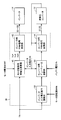
- FIG. 1 is a schematic block diagram illustrating the configuration of an electric motor drive device 100 according to Embodiment 1 of the present invention.
- an electric motor drive device 100 includes a power storage mechanism B, voltage sensors 10, 13, system relays SR1, SR2, a step-up / down converter 12, a discharge resistor R1, , A smoothing capacitor C2, an inverter 14, a current sensor 24, an AC motor M1, and a control device 30.
- AC motor M1 is a drive motor for generating torque for driving drive wheels of a hybrid vehicle or an electric vehicle, for example.
- this motor has the function of a generator driven by an engine, and operates as an electric motor for the engine, for example, can be incorporated into a hybrid vehicle so that the engine can be started. Also good.
- the power storage mechanism B is configured to include a secondary battery such as nickel metal hydride or lithium ion, and outputs a DC voltage between the power supply line 6 and the earth line 5.
- Voltage sensor 10 detects a DC voltage (battery voltage) Vb output from power storage mechanism B, and outputs the detected DC voltage Vb to control device 30.
- System relay SR1 is connected between the positive terminal of power storage mechanism B and power supply line 6, and system relay SR2 is connected between the negative terminal of power storage mechanism B and ground line 5.
- System relays SR1 and SR2 are turned on / off by signal SE from control device 30.
- the step-up / down converter 12 includes a step-up / step-down chopper circuit, and includes a reactor L1, power semiconductor switching elements (hereinafter also simply referred to as switching elements) Q1, Q2, and diodes D1, D2.
- switching elements power semiconductor switching elements
- the switching elements Q1 and Q2 are connected in series between the power supply line 7 and the earth line 5.
- Reactor L1 is connected between power supply line 6 and a connection node of switching elements Q1 and Q2.
- Anti-parallel diodes D1 and D2 are connected between the emitters / collectors of switching elements Q1 and Q2, respectively, so that current flows from the emitter side to the collector side.
- Switching elements Q1 and Q2 are turned on / off by switching control signals S1, S2 from control device 30.
- a switching element in this embodiment for example, IGBT (Insulated Gate Bipolar Transistor) is applied.
- the smoothing capacitor C2 is connected between the power supply line 7 and the earth line 5. Further, between the power supply line 7 and the earth line 5, a discharge resistor R1 for removing the residual charge of the smoothing capacitor C2 when the motor driving device 100 is stopped is connected in parallel to the smoothing capacitor C2.
- the inverter 14 includes a U-phase arm 15, a V-phase arm 16, and a W-phase arm 17 connected in parallel between the power supply line 7 and the earth line 5.
- Each phase arm is composed of a switching element connected in series between the power supply line 7 and the earth line 5.
- U-phase arm 15 includes switching elements Q3 and Q4
- V-phase arm 16 includes switching elements Q5 and Q6
- W-phase arm 17 includes switching elements Q7 and Q8.
- Antiparallel diodes D3 to D8 are connected between the collectors / emitters of switching elements Q3 to Q8, respectively.
- the on / off of the switching elements Q3 to Q8 is controlled by switching control signals S3 to S8 from the control device 30. More specifically, switching elements Q3-Q8 are turned on or off according to the electrical input to their control electrodes. For example, the IGBT is turned on or off according to the voltage of the gate (control electrode). Switching control signals S3 to S8 are input to the control electrodes (gates) of the switching elements Q3 to Q8 through a drive circuit (not shown).
- each phase arm 15 to 17 is electrically connected to one end side of U-phase coil winding 20U, V-phase coil winding 20V and W-phase coil winding 20W of AC motor M1.
- AC motor M1 is a three-phase permanent magnet motor configured by commonly connecting U-phase coil winding 20U, V-phase coil winding 20V and W-phase coil winding 20W to a neutral point.
- U-phase coil winding 20U, V-phase coil winding 20V and W-phase coil winding 20W correspond to “coil winding” in the present invention.
- AC motor M1 corresponds to the “motor” in the present invention.
- AC motor M1 is provided with a current sensor 24.
- Current sensor 24 detects motor current MCRT (U-phase current, V-phase current and W-phase current) for three phases, and sends the detected motor current MCRT to control device 30. Since the sum of instantaneous values of the three-phase currents is zero, it is sufficient that the current sensor 24 is disposed so as to detect the motor current for two phases.
- the step-up / step-down converter 12 boosts the DC voltage supplied from the power storage mechanism B and supplies it to the inverter 14 during the boosting operation. More specifically, in response to switching control signals S1 and S2 from control device 30, an ON period of switching element Q1 and an ON period of Q2 are alternately provided, and the step-up ratio depends on the ratio of these ON periods. It will be.
- the step-up / down converter 12 steps down the DC voltage supplied from the inverter 14 via the smoothing capacitor C2 and charges the power storage mechanism B. More specifically, in response to switching control signals S1 and S2 from control device 30, a period in which only switching element Q1 is turned on and a period in which both switching elements Q1 and Q2 are turned off are provided alternately. The ratio depends on the duty ratio of the on period.
- the smoothing capacitor C2 smoothes the DC voltage from the step-up / down inverter 12 and supplies the smoothed DC voltage to the inverter 14.
- the voltage sensor 13 detects the voltage VH across the smoothing capacitor C2, that is, the output voltage of the buck-boost converter 12 (corresponding to the input voltage of the inverter 14, the same applies hereinafter), and the detected voltage VH is controlled by the control device 30. Output to.
- the inverter 14 converts the DC voltage into an AC voltage by the switching operation of the switching elements Q3 to Q8 in response to the switching control signals S3 to S8 from the control device 30.
- the motor M1 is driven.
- the inverter 14 converts the AC voltage generated by the AC motor M1 into a DC voltage by switching operation in response to the switching control signals S3 to S8 during regenerative braking of the hybrid vehicle or electric vehicle on which the electric motor driving device 100 is mounted. Then, the converted DC voltage is supplied to the step-up / down converter 12 via the smoothing capacitor C2.
- regenerative braking refers to braking involving regenerative power generation when a driver operating a hybrid vehicle or electric vehicle performs a footbrake operation, or while not operating the footbrake, It includes decelerating (or stopping acceleration) the vehicle speed while generating regenerative power by turning it off.
- Control device 30 receives torque command value TR and motor rotational speed MRN from an externally provided ECU (Electrical Control Unit), receives DC voltage Vb from voltage sensor 10, receives voltage VH from voltage sensor 13, and current sensor. 24 receives motor current MCRT. Based on these input signals, control device 30 controls the operations of buck-boost converter 12 and inverter 14 such that AC motor M1 outputs a torque according to torque command value TR by a method described later. That is, switching control signals S1 to S8 for controlling the buck-boost converter 12 and the inverter 14 as described above are generated and output to the buck-boost converter 12 and the inverter 14.
- ECU Electronic Control Unit
- the control device 30 switches the switching elements Q3 to Q8 so that an AC voltage that allows the AC motor M1 to output a torque according to the torque command value TR is applied to the phase coil windings 20U, 20V, and 20W. Controls the switching operation. That is, the control device 30 generates switching control signals S3 to S8 corresponding to such a switching operation.
- the alternating voltage applied to each phase coil winding 20U, 20V, and 20W is also called "motor drive voltage.”
- switching control signals S3 to S8 generated by the control device 30 are given to a drive circuit (not shown).
- the drive circuit generates gate voltages for turning on or off switching elements Q3 to Q8, respectively, in response to switching control signals S3 to S8.
- FIG. 2 is a block diagram of the control device 30 in FIG. Referring to FIG. 2, control device 30 includes a motor control phase voltage calculation unit 40, an inverter PWM signal conversion unit 42, an inverter input voltage command calculation unit 50, a converter duty ratio calculation unit 52, and a converter. PWM signal converter 54 for use.
- Motor control phase voltage calculation unit 40 receives torque command value TR from an external ECU, receives output voltage VH of step-up / down converter 12 from voltage sensor 13, that is, an input voltage of inverter 14, and receives motor current MCRT from current sensor 24. Receive. Based on these input signals, the motor control phase voltage calculation unit 40 operates an operation amount (hereinafter also referred to as a voltage command) Vu of a voltage (motor drive voltage) applied to each phase coil winding of the AC motor M1. *, Vv *, Vw * are calculated, and the calculated results are output to the inverter PWM signal converter 42.
- a voltage command hereinafter also referred to as a voltage command
- the inverter PWM signal conversion unit 42 actually sets each switching element Q3 ⁇ of the inverter 14 based on the voltage commands Vu *, Vv *, Vw * of the respective phase coil windings received from the motor control phase voltage calculation unit 40. Switching control signals S3 to S8 for turning on / off Q8 are generated and output to inverter 14.
- each of the switching elements Q3 to Q8 is subjected to switching control, and controls the current flowing through each phase coil winding of the AC motor M1 so that the AC motor M1 outputs the commanded torque.
- the motor drive current is controlled, and a motor torque corresponding to the torque command value TR is output.
- Inverter input voltage command calculation unit 50 calculates the optimum value (target value) of the inverter input voltage, that is, voltage command Vdc_com, based on torque command value TR and motor rotation speed MRN from the external ECU, and the calculated voltage command Vdc_com is output to converter duty-ratio calculation unit 52.
- converter duty-ratio calculation unit 52 receives voltage command Vdc_com from inverter input voltage command calculation unit 50 and DC voltage Vb (hereinafter also referred to as battery voltage Vb) from voltage sensor 10, output voltage from voltage sensor 13 is output. A duty ratio for setting VH to the voltage command Vdc_com is calculated. Then, converter duty-ratio calculation unit 52 outputs the calculated duty ratio to converter PWM signal conversion unit 54.
- Converter PWM signal converter 54 generates switching control signals S1 and S2 for turning on / off switching elements Q1 and Q2 of buck-boost converter 12 based on the duty ratio from converter duty ratio calculator 52. Output to the step-up / down converter 12.
- the power accumulation of the reactor L1 is increased by increasing the on-duty of the switching element Q2 on the lower side of the step-up / down converter 12, a higher voltage output can be obtained.
- increasing the on-duty of the upper switching element Q1 reduces the voltage of the power supply line. Therefore, by controlling the duty ratios of the switching elements Q1 and Q2, the input voltage VH of the inverter 14 is reduced to the upper limit value set based on the element withstand voltage of the switching element, etc., with the output voltage of the power storage mechanism B as the lower limit. It can be controlled to an arbitrary voltage.
- the input voltage VH of the inverter 14 is varied according to the operating state of the AC motor M1, thereby causing a loss (motor loss, inverter loss) generated in the electric motor drive device 100. And the boost converter loss) and the motor drive efficiency can be increased.
- the inverter 14 converts the input voltage VH converted to a high voltage equal to or higher than the output voltage of the power storage mechanism B into an AC voltage (motor drive voltage) by the switching operation of the switching elements Q3 to Q8 to drive the AC motor M1. To do.
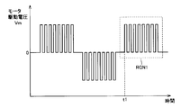
- FIG. 3 is an output waveform diagram of an AC voltage (motor drive voltage) Vm generated by the switching operation of the switching elements Q3 to Q8.
- the motor drive voltage Vm is a bipolar pulse voltage whose polarity is reversed every half cycle.
- the pulse voltage having the same polarity during the half cycle has a predetermined voltage amplitude and a predetermined pulse width.
- the predetermined voltage amplitude at this time has a magnitude corresponding to the voltage commands Vu *, Vv *, and Vw * of each phase coil winding of the AC motor M1 described above.
- the predetermined pulse width corresponds to the carrier frequency of the carrier signal for generating the switching control signals S3 to S8 of the inverter 14.
- FIG. 4 is a diagram showing a partial discharge measurement waveform when the motor drive voltage Vm of FIG. 3 is applied to each phase coil winding.
- FIG. 4 shows an extracted partial discharge waveform measured when the motor drive voltage Vm exhibits the characteristics in the region RGN1 of FIG.
- motor drive voltage Vm is composed of a pulse voltage of the same polarity having a predetermined voltage amplitude and pulse width in a half cycle.
- the motor drive voltage Vm is set to a negative potential before time t1, and after passing through the zero potential, is set to a positive potential at time t1.
- time t1 which is the timing when the first pulse voltage rises when the polarity of the motor drive voltage Vm is reversed
- partial discharge is generated in the gap between the coil windings.
- the partial discharge at this time is significantly larger than the minute discharge generated at time t2, t3, etc. after the time t1 and at the timing when the second and subsequent pulse voltages rise.
- the motor driving voltage Vm is a pulse voltage as shown in FIG. 4, the polarity inversion of the motor driving voltage Vm is performed in a short time.
- Insulating film surface of the other coil winding conductor that is newly set from negative potential to positive potential at the time of reversal in the state that the surface charge induced on the insulating film surface of the coil winding conductor remains undiffused Surface charge begins to be induced in the surface.
- the gap voltage between the coil windings is increased by the electric field generated by the surface charge in the gap between the coil windings.
- discharge partial discharge
- the partial discharge start voltage is lowered by increasing the electric field generated by the surface charge in the gap.
- the deterioration of the insulating film may eventually lead to a short circuit between the interphase insulations and shorten the insulation life.
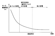
- FIG. 5 is a diagram showing the relationship between the motor drive voltage Vm and the insulation life of each phase coil winding of the AC motor M1.
- each phase coil winding of AC motor M1 shows a tendency to increase as motor drive voltage Vm decreases. This is because the partial discharge generated in the gap between each phase coil winding is roughly divided into three generation patterns according to the magnitude of the motor drive voltage Vm.
- the surface charge induced on the insulating film surface of the coil winding is diffused when the polarity of the motor driving voltage Vm is reversed. It is necessary to secure time. For this purpose, it is effective to moderate the polarity inversion of the motor drive voltage Vm. That is, by reducing the voltage change rate of the motor drive voltage Vm at the time of polarity reversal, the electric field generated by the surface charge in the gap can be weakened. As a result, the partial discharge start voltage can be prevented from decreasing.
- the rise of the first pulse voltage (see the region RGN2 in FIG. 4) at the time of polarity reversal.
- the switching operation of the inverter 14 is controlled so that the time becomes relatively longer than the remaining pulse voltage that follows.
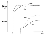
- FIG. 6 is a measurement waveform of the first pulse voltage when the polarity of the motor drive voltage Vm is reversed and the partial discharge generated when the pulse voltage is applied to each phase coil winding of the AC motor M1.
- lines LN1 and LN3 respectively show the first pulse voltage and the measured waveform of the partial discharge when the polarity of the motor drive voltage Vm generated by the normal switching control is reversed.
- lines LN2 and LN4 in the figure respectively show the first pulse voltage and the partial discharge measurement waveform at the time of polarity reversal generated by performing control to reduce the voltage change rate of the motor drive voltage Vm at the time of polarity reversal. Show.
- FIG. 6 shows that the occurrence of partial discharge is suppressed between the gaps of the coil windings of each phase by increasing the rise time of the first pulse voltage at the time of polarity reversal. That is, a situation where an electric field generated by surface charges remaining in the gap of the coil winding increases the gap voltage and partial discharge is likely to occur is avoided. Thereby, generation
- the drive circuit for generating the gate voltage can be realized by adopting a configuration in which the gate resistance can be variably set between the first pulse voltage and the remaining pulse voltage.
- FIG. 7 is an electric circuit diagram showing an example of a drive circuit that makes the rise time of the pulse voltage variable.
- the drive circuit includes resistors RG1 and RG2, switching elements Q11 and Q12, and a current supply line BL.
- Resistors RG1 and RG2 have one end connected to the base of a switching element (for example, Q3) of inverter 14 and the other end connected to the emitters of switching elements Q11 and Q12.
- Switching elements Q11 and Q12 have their collectors connected to current supply line BL, their emitters connected to resistors RG1 and RG2, and receive switching control signals from control device 30 on their bases.
- the resistance value of the resistor RG1 is larger than the resistance value of the resistor RG2. Therefore, by selecting the resistor RG1 having a relatively large resistance value when the polarity of the motor drive voltage Vm is reversed, the collector-emitter voltage at the time of turn-on and turn-off is relatively gentle in each of the switching elements Q3 to Q8. Waveform. As a result, the rise time at the time of polarity reversal of the motor drive voltage Vm can be made relatively long.
- the switching elements Q3 to Q8 are turned on and off.
- FIG. 8 is a flowchart for explaining a switching control process of inverter 14 in electric motor drive device 100 according to the first embodiment of the present invention.
- the control process according to the flowchart shown in FIG. 8 is realized by the control device 30 executing a program stored in advance at predetermined intervals.
- control device 30 that functions as inverter PWM signal conversion unit 42 receives voltage commands Vu * and Vv * for each phase coil winding from control device 30 that functions as motor control phase voltage calculation unit 40. , Vw * (step S01), it is determined whether or not these voltage commands Vu *, Vv *, Vw * are equal to or higher than a predetermined threshold value Vth1 (step S02).
- the predetermined threshold value Vth1 generates a minute discharge in the gap between the phase coil windings based on the relationship between the motor drive voltage Vm shown in FIG. 5 and the insulation life of each phase coil winding of the AC motor M1. Is set to exceed the motor drive voltage Vm at the time.
- control device 30 that functions as inverter PWM signal converter 42 constitutes inverter 14.
- Switching control signals S3 to S8 for actually turning on / off the switching elements Q3 to Q8 of the inverter 14 are generated by executing normal switching control on the switching elements Q3 to Q8 (step S04). .
- the resistor RG2 is selected in the drive circuit shown in FIG.
- control device 30 that functions as inverter PWM signal conversion unit 42 is Then, the switching control signals S3 to S8 are generated so that the rising time of the first pulse voltage when the polarity of the motor drive voltage Vm is reversed is relatively long (step S03).
- the control device 30 uses the drive circuit shown in FIG. 7 to variably set the gate resistance between the first pulse voltage and the remaining pulse voltage when the polarity of the motor drive voltage Vm is reversed. . As a result, generation of interphase dielectric breakdown between the coil windings can be prevented by preventing the occurrence of partial discharge.
- the gate resistance in the switching operation of the inverter 14 is variably set between the first pulse voltage and the remaining pulse voltage at the time of polarity inversion, but is limited to the gate resistance. Without delay, the delay impedance in the path through which the switching control signals S3 to S8 from the control device 30 are transmitted to the gates (control electrodes) of the switching elements Q3 to Q8, the first pulse voltage and the remaining pulse voltage at the time of polarity inversion Obviously, it may be variably set between the two. That is, the same effect can be obtained even when the capacitance value or inductance value to be added is variably set instead of the resistance component (gate resistance) in the transmission path.
- variable setting of the delay impedance typified by the gate resistance is set in two steps according to the first pulse voltage at the time of polarity reversal and the remaining pulse voltage.
- the pulse voltage may be further subdivided and the delay impedance may be variably set in three or more stages.
- the delay impedance may be continuously variably set so that the delay impedance is gradually extended as the motor drive voltage Vm increases. According to this, it is possible to effectively prevent the occurrence of partial discharge while suppressing the loss generated in each of the switching elements Q3 to Q8.
- FIG. 9 is a flowchart for illustrating a switching control process of inverter 14 in the motor drive device according to the modification of the first embodiment of the present invention.
- the control process according to the flowchart shown in FIG. 9 is realized by the control device 30 executing a program stored in advance at predetermined intervals.
- control device 30 that functions as inverter PWM signal conversion unit 42 receives voltage commands Vu * and Vv * for each phase coil winding from control device 30 that functions as motor control phase voltage calculation unit 40. , Vw * (step S01), it is determined whether or not these voltage commands Vu *, Vv *, Vw * are equal to or higher than a predetermined threshold value Vth2 (step S021).
- the predetermined threshold value Vth2 is determined based on the relationship between the motor drive voltage Vm shown in FIG. 5 and the insulation life of each phase coil winding of the AC motor M1.
- the motor drive voltage Vm at the time when this occurs is set to include the lower limit value.
- control device 30 that functions as inverter PWM signal conversion unit 42 constitutes inverter 14.
- Switching control signals S3 to S8 for actually turning on / off the switching elements Q3 to Q8 of the inverter 14 are generated by executing normal switching control on the switching elements Q3 to Q8 (step S04). .
- the resistor RG2 is selected in the drive circuit shown in FIG.
- step S021 when the voltage commands Vu *, Vv *, Vw * are equal to or higher than the predetermined threshold Vth2 (YES in step S021), the control device 30 that functions as the inverter PWM signal conversion unit 42 is Then, the switching control signals S3 to S8 are generated so that the rising times of all the pulse voltages of the same polarity constituting the motor drive voltage Vm are relatively long (step S031). Specifically, the control device 30 sets the gate resistance to a relatively high resistance value for all pulse voltages having the same polarity using the drive circuit shown in FIG. As a result, even in a situation where the motor drive voltage Vm is relatively high and partial discharge is more likely to occur, partial discharge can be reliably prevented, thereby preventing interphase dielectric breakdown between coil windings. it can.
- the capacitance of the smoothing capacitor C2 provided on the input side of the inverter 14 is not limited to the configuration in which the gate resistance is increased. It can also be performed by adjusting the resistance value of the discharge resistor R1.
- FIG. 10 is a schematic block diagram illustrating a configuration of an electric motor drive device 100A according to the second embodiment of the present invention.
- electric motor drive device 100A is different from electric motor drive device 100 shown in FIG. 1 in that step-up / down converter 12A is provided instead of step-up / down converter 12. Since the configuration of other parts of motor drive device 100A is the same as that of motor drive device 100 shown in FIG. 1, detailed description will not be repeated.
- the buck-boost converter 12A is a switching circuit for directly connecting the power line 6 and the power line 7 without the reactor L1 and the switching element Q1 to the buck-boost converter 12 configured by the buck-boost chopper circuit. It further includes an element Qb.
- the switching element Qb is turned on or off by a switching control signal Sb from the control device 30A.
- switching element Qb When switching element Qb is turned on, the direct current from power storage mechanism B flows to power supply line 7 via switching element Qb. Therefore, no current is supplied to reactor L1, so that the boosting operation is not performed, and input voltage VH of inverter 14 is approximately the same voltage level as the output voltage of power storage mechanism B.
- the switching element Qb corresponds to a “bypass switching element” in the present invention.
- FIG. 11 is a block diagram of the control device 30A in FIG. Referring to FIG. 11, control device 30 ⁇ / b> A differs from control device 30 shown in FIG. 2 in that converter PWM signal conversion unit 54 ⁇ / b> A is provided instead of converter PWM signal conversion unit 54. Since the configuration of other parts of control device 30A is the same as that of control device 30 shown in FIG. 2, detailed description will not be repeated.
- Converter PWM signal converter 54A receives the duty ratio from converter duty ratio calculator 52, receives input voltage VH of inverter 14 from voltage sensor 13, and receives the voltage of each phase coil winding from inverter PWM signal converter 42. Receives commands Vu *, Vv *, Vw *. Then, converter PWM signal converter 54A generates switching control signals S1, S2 for turning on / off switching elements Q1, Q2 of buck-boost converter 12A based on the duty ratio, and outputs the switching control signals S1, S2 to buck-boost converter 12A. .
- converter PWM signal converter 54A determines whether or not voltage commands Vu *, Vv *, and Vw * are equal to or higher than a predetermined threshold value Vth1. When the voltage commands Vu *, Vv *, and Vw * are equal to or greater than the predetermined threshold value Vth1, the converter PWM signal converter 54A switches the switching control signal Sb for turning on the switching element Qb that constitutes the bypass switching element. And output to the switching element Qb. Thereby, switching element Qb is turned on, and input voltage VH of inverter 14 becomes substantially equal to the output voltage of power storage mechanism B.
- the converter PWM signal converter 54A detects the timing at which the polarity of the motor drive voltage Vm is reversed based on the voltage commands Vu *, Vv *, Vw *, and temporarily switches the switching control signal at the detected timing. Sb is generated and output to the switching element Qb. As a result, when the polarity of the motor drive voltage Vm is reversed, a voltage substantially equal to the output voltage of the power storage mechanism B is temporarily input to the inverter 14.
- FIG. 12 is an output waveform diagram of AC voltage (motor drive voltage) Vm generated by the switching operation of switching elements Q3 to Q8 according to the second embodiment.
- motor drive voltage Vm is a bipolar pulse voltage whose polarity is inverted every half cycle, as in the first embodiment.
- the voltage amplitude of the first pulse voltage (see reference numeral 60 in the figure) when the polarity of the motor drive voltage Vm is reversed is the remaining pulse voltage that follows.
- the voltage amplitude is relatively smaller. This is substantially equivalent to a small voltage change rate when the polarity of the motor drive voltage Vm is reversed. Therefore, also in the second embodiment, the occurrence of partial discharge between the gaps of the respective phase coil windings is suppressed, and the occurrence of interphase dielectric breakdown between the coil windings can be prevented.
- FIG. 13 is a flowchart for illustrating a switching control process of inverter 14 in electric motor drive device 100A according to the second embodiment of the present invention.
- the control process according to the flowchart shown in FIG. 13 is realized by the control device 30A executing a program stored in advance at predetermined intervals.
- control device 30 ⁇ / b> A functioning as converter PWM signal conversion unit 54 ⁇ / b> A receives voltage commands Vu *, Vv *, When Vw * is acquired (step S01), it is determined whether or not these voltage commands Vu *, Vv *, Vw * are equal to or higher than a predetermined threshold value Vth1 (step S02).
- the predetermined threshold Vth1 is determined based on the relationship between the motor drive voltage Vm shown in FIG. 5 and the insulation life of each phase coil winding of AC motor M1. It is set to exceed the motor drive voltage Vm when a minute discharge occurs in the gap.
- control device 30A that functions as converter PWM signal converter 54A causes step-up / step-down converter 12 to operate.
- Switching control signals S1 and S2 for turning on / off switching elements Q1 and Q2 are generated by performing normal voltage conversion control on switching elements Q1 and Q2 to be configured (step S042). In this case, switching element Qb is maintained in the OFF state in motor drive device 100A shown in FIG.
- control device 30A that functions as converter PWM signal converter 54A is The switching control signals S1, S2, and Sb are generated so that the voltage amplitude of the first pulse voltage becomes relatively small when the polarity of the motor drive voltage Vm is reversed (step S032). Specifically, the control device 30A sets the voltage amplitude to be variable between the first pulse voltage and the remaining pulse voltage when the polarity of the motor drive voltage Vm is reversed by turning on / off the switching element Qb. To do. As a result, generation of interphase dielectric breakdown between the coil windings can be prevented by preventing the occurrence of partial discharge.
- FIG. 14 is a schematic block diagram illustrating a configuration of an electric motor drive device 100B according to the third embodiment of the present invention.
- electric motor drive device 100 ⁇ / b> B according to the third embodiment further includes an inverter 31 connected in parallel to inverter 14 with respect to AC motor M ⁇ b> 1 as compared with electric motor drive device 100 shown in FIG. 1. It is different in point. Since the configuration of other parts of motor drive device 100B is similar to that of motor drive device 100 shown in FIG. 1, detailed description will not be repeated.
- the inverter 31 has the same configuration as the inverter 14 although not shown.
- inverter 31 includes a U-phase arm, a V-phase arm, and a W-phase arm provided in parallel between power supply line 7 and earth line 5.
- Each phase arm is composed of switching elements connected in series.
- the intermediate point of each phase arm is connected to each phase end of each phase coil winding 20U, 20V, 20W of AC motor M1.
- the inverter 31 When the DC voltage VH is supplied from the smoothing capacitor C2, the inverter 31 is switched from the DC voltage VH by switching operations of switching elements Q3 to Q8 (not shown) in response to the switching control signals S13 to S18 from the control device 30B. Generate a pulse voltage. Then, the generated pulse voltage is applied to each phase coil winding of AC motor M1.
- the pulse voltage from the inverter 31 is applied to each phase coil winding of the AC motor M1.
- FIG. 15 is an output waveform diagram of a voltage applied to each phase coil winding of AC motor M1 by the switching operation of inverters 14 and 31 according to the third embodiment.
- motor driving voltage Vm from inverter 14 is applied to each phase coil winding.
- the motor drive voltage Vm is a bipolar pulse voltage whose polarity is inverted every half cycle, as in the first embodiment.
- a pulse voltage (see reference numeral 62 in the figure) is further applied from the inverter 31 during a period of passing through the zero potential when the polarity of the motor drive voltage Vm is reversed.
- the switching operation of the inverter 31 is controlled so as to generate a pulse voltage every half cycle of the motor drive voltage Vm.
- the voltage amplitude of the pulse voltage is set to a value smaller than the voltage amplitude of the pulse voltage constituting the motor drive voltage Vm.
- the AC voltage applied to each phase coil winding generally has a waveform in which the voltage rise at the time of polarity inversion is gentle.
- the voltage change rate at the time of polarity reversal of the motor drive voltage Vm can be reduced, the occurrence of partial discharge between the gaps of the respective phase coil windings can also be suppressed in the third embodiment. And the occurrence of interphase dielectric breakdown between the coil windings can be prevented.
- FIG. 16 is a flowchart for illustrating a switching control process of inverter 31 in electric motor drive device 100B according to the third embodiment of the present invention.
- the control process according to the flowchart shown in FIG. 16 is realized by the control device 30B executing a program stored in advance at predetermined intervals.
- control device 30B that functions as inverter PWM signal conversion unit 42 receives voltage commands Vu * and Vv * for each phase coil winding from control device 30B that functions as motor control phase voltage calculation unit 40. , Vw * (step S01), it is determined whether or not these voltage commands Vu *, Vv *, Vw * are equal to or higher than a predetermined threshold value Vth1 (step S02).
- the predetermined threshold Vth1 is determined based on the relationship between the motor drive voltage Vm shown in FIG. 5 and the insulation life of each phase coil winding of AC motor M1. It is set to exceed the motor drive voltage Vm when a minute discharge occurs in the gap.
- control device 30B that functions as inverter PWM signal conversion unit 42 operates inverter 31. Stop (step S043). Specifically, the inverter PWM signal conversion unit 42 generates the switching control signals S13 to S18 so that each of the switching elements Q3 to Q8 constituting the inverter 31 stops the switching operation (all are turned off).
- control device 30B that functions as inverter PWM signal conversion unit 42 is The switching control signals S13 to S18 are generated and output to the inverter 31 so that a pulse voltage is generated from the inverter 31 during the period when the polarity of the motor driving voltage Vm is reversed when passing through the zero potential (step S033).
- control device 30B functioning as the inverter PWM signal conversion unit 42 actually sets each switching element of the inverter 14 based on the voltage commands Vu *, Vv *, Vw *. Switching control signals S3 to S8 for turning on / off Q3 to Q8 are generated.
- the present invention can be applied to a power supply device mounted on a hybrid vehicle.
Abstract
Description
図1は、この発明の実施の形態1による電動機駆動装置100の構成を説明する概略ブロック図である。 [Embodiment 1]
FIG. 1 is a schematic block diagram illustrating the configuration of an electric
Gate Bipolar Transistor)が適用される。 Switching elements Q1 and Q2 are turned on / off by switching control signals S1, S2 from
Gate Bipolar Transistor) is applied.
図2を参照して、制御装置30は、モータ制御用相電圧演算部40と、インバータ用PWM信号変換部42と、インバータ入力電圧指令演算部50と、コンバータ用デューティー比演算部52と、コンバータ用PWM信号変換部54とを含む。 FIG. 2 is a block diagram of the
Referring to FIG. 2,
図9は、この発明の実施の形態1の変更例による電動機駆動装置におけるインバータ14のスイッチング制御処理を説明するためのフローチャートである。図9に示したフローチャートに従う制御処理は、制御装置30が予め格納されたプログラムを所定周期毎に実行することにより実現される。 [Example of change]
FIG. 9 is a flowchart for illustrating a switching control process of
図10は、この発明の実施の形態2に従う電動機駆動装置100Aの構成を説明する概略ブロック図である。 [Embodiment 2]
FIG. 10 is a schematic block diagram illustrating a configuration of an electric
図11を参照して、制御装置30Aは、図2に示す制御装置30と比較して、コンバータ用PWM信号変換部54に代えて、コンバータ用PWM信号変換部54Aを備える点で異なる。制御装置30Aのその他の部分の構成は図2に示した制御装置30と同様であるので詳細な説明は繰り返さない。 FIG. 11 is a block diagram of the
Referring to FIG. 11,
図14は、この発明の実施の形態3に従う電動機駆動装置100Bの構成を説明する概略ブロック図である。 [Embodiment 3]
FIG. 14 is a schematic block diagram illustrating a configuration of an electric
Claims (16)
- 電力用半導体素子のスイッチング動作によって交流電圧を発生する電力変換装置と、
前記電力変換装置からの交流電圧が印加されるコイル巻線(20U,20V,20W)を有する電動機(M1)と、
前記電力変換装置のスイッチング動作を制御する制御装置(30)とを備え、
前記制御装置(30,30A,30B)は、前記交流電圧が所定値を超えるときには、前記交流電圧の極性反転時における電圧変化率が相対的に小さくなるように、前記電力変換装置のスイッチング動作を制御する、電動機駆動装置。 A power converter that generates an alternating voltage by switching operation of a power semiconductor element;
An electric motor (M1) having a coil winding (20U, 20V, 20W) to which an AC voltage from the power converter is applied;
A control device (30) for controlling the switching operation of the power converter,
When the AC voltage exceeds a predetermined value, the control device (30, 30A, 30B) performs the switching operation of the power converter so that the voltage change rate at the time of polarity reversal of the AC voltage becomes relatively small. An electric motor drive device to be controlled. - 前記電力変換装置は、前記電力用半導体素子のスイッチング動作によって、前記交流電圧として、所定の電圧振幅および所定のパルス幅を有する両極性パルス電圧を発生するインバータ(14)を含み、
前記制御装置(30)は、前記所定の電圧振幅が前記所定値を超えるときには、前記両極性パルス電圧の極性反転時における立ち上がり時間が相対的に長くなるように、前記インバータ(14)のスイッチング動作を制御する、請求の範囲第1項に記載の電動機駆動装置。 The power converter includes an inverter (14) that generates a bipolar pulse voltage having a predetermined voltage amplitude and a predetermined pulse width as the AC voltage by the switching operation of the power semiconductor element,
When the predetermined voltage amplitude exceeds the predetermined value, the control device (30) performs the switching operation of the inverter (14) so that the rise time at the time of polarity reversal of the bipolar pulse voltage is relatively long. The electric motor drive device according to claim 1, which controls the motor. - 前記インバータ(14)は、各前記電力用半導体素子の制御電極に駆動制御信号を伝達する経路を含み、
前記制御装置(30)は、前記所定の電圧振幅が前記所定値を超えるときには、前記両極性パルスの極性反転時において、前記経路の遅延インピーダンスを相対的に高く設定する、請求の範囲第2項に記載の電動機駆動装置。 The inverter (14) includes a path for transmitting a drive control signal to the control electrode of each power semiconductor element;
The control device (30), when the predetermined voltage amplitude exceeds the predetermined value, sets the delay impedance of the path relatively high at the time of polarity inversion of the bipolar pulse. The electric motor drive device described in 1. - 前記電力変換装置は、前記電力用半導体素子のスイッチング動作によって、前記交流電圧として、所定の電圧振幅および所定のパルス幅を有する両極性パルス電圧を発生するインバータ(14)を含み、
前記制御装置(30)は、前記所定の電圧振幅が前記所定値を超えるときには、前記両極性パルスの立ち上がり時間が相対的に長くなるように、前記インバータ(14)のスイッチング動作を制御する、請求の範囲第1項に記載の電動機駆動装置。 The power converter includes an inverter (14) that generates a bipolar pulse voltage having a predetermined voltage amplitude and a predetermined pulse width as the AC voltage by the switching operation of the power semiconductor element,
The control device (30) controls the switching operation of the inverter (14) so that a rising time of the bipolar pulse becomes relatively long when the predetermined voltage amplitude exceeds the predetermined value. The electric motor drive device according to claim 1, wherein - 前記インバータ(14)は、各前記電力用半導体素子の制御電極に駆動制御信号を伝達する経路を含み、
前記制御装置(30)は、前記所定の電圧振幅が前記所定値を超えるときには、前記経路の遅延インピーダンスを相対的に高く設定する、請求の範囲第4項に記載の電動機駆動装置。 The inverter (14) includes a path for transmitting a drive control signal to the control electrode of each power semiconductor element;
The electric motor drive device according to claim 4, wherein the control device (30) sets the delay impedance of the path to be relatively high when the predetermined voltage amplitude exceeds the predetermined value. - 前記電力変換装置は、
前記電力用半導体素子のスイッチング動作によって、前記交流電圧として、所定の電圧振幅および所定のパルス幅を有する両極性パルス電圧を発生するインバータ(14)と、
前記電力用半導体素子のスイッチング動作によって、前記インバータ(14)への入力電圧を可変制御可能に構成された直流電源とを含み、
前記制御装置(30A)は、前記交流電圧が前記所定値を超えるときには、前記交流電圧の極性反転時における前記入力電圧が相対的に低くなるように、前記直流電源のスイッチング動作を制御する、請求の範囲第1項に記載の電動機駆動装置。 The power converter is
An inverter (14) for generating a bipolar pulse voltage having a predetermined voltage amplitude and a predetermined pulse width as the AC voltage by the switching operation of the power semiconductor element;
A DC power source configured to be able to variably control the input voltage to the inverter (14) by the switching operation of the power semiconductor element,
The control device (30A) controls the switching operation of the DC power supply so that when the AC voltage exceeds the predetermined value, the input voltage at the time of polarity inversion of the AC voltage becomes relatively low. The electric motor drive device according to claim 1, wherein - 前記直流電源は、
前記電力用半導体素子のスイッチング動作によって蓄電機構(B)からの直流電圧を電圧変換するコンバータ(12)と、
前記蓄電機構(B)と前記インバータ(14)との間に前記コンバータをバイパスするように電流経路を形成するためのバイパス用スイッチング素子(Qb)とを含み、
前記制御装置(30A)は、前記交流電圧が前記所定値を超えるときには、前記交流電圧の極性反転時において、前記バイパス用スイッチング素子(Qb)をオンする、請求の範囲第6項に記載の電動機駆動装置。 The DC power supply is
A converter (12) for converting a DC voltage from the power storage mechanism (B) by a switching operation of the power semiconductor element;
A bypass switching element (Qb) for forming a current path so as to bypass the converter between the power storage mechanism (B) and the inverter (14);
The electric motor according to claim 6, wherein the control device (30A) turns on the bypass switching element (Qb) during polarity reversal of the AC voltage when the AC voltage exceeds the predetermined value. Drive device. - 前記電力変換装置は、
前記電力用半導体素子のスイッチング動作によって、前記交流電圧として、所定の電圧振幅および所定のパルス幅を有する両極性パルス電圧を発生するインバータ(14)と、
前記コイル巻線に対して前記インバータ(14)と並列に接続され、前記電力用半導体素子のスイッチング動作によって、前記コイル巻線にパルスを印加可能に構成されたパルス発生装置(31)をさらに備え、
前記制御装置(30B)は、前記交流電圧が前記所定値を超えるときには、前記交流電圧の極性反転時において、前記交流電圧が零電位であるときに、前記交流電圧よりも相対的に小さい電圧振幅を有するパルスを前記コイル巻線に印加するように、前記パルス発生装置(31)を制御する、請求の範囲第1項に記載の電動機駆動装置。 The power converter is
An inverter (14) for generating a bipolar pulse voltage having a predetermined voltage amplitude and a predetermined pulse width as the AC voltage by the switching operation of the power semiconductor element;
A pulse generator (31) connected to the coil winding in parallel with the inverter (14) and configured to be able to apply a pulse to the coil winding by a switching operation of the power semiconductor element. ,
When the AC voltage exceeds the predetermined value, the control device (30B) has a voltage amplitude that is relatively smaller than the AC voltage when the AC voltage is zero potential when the polarity of the AC voltage is inverted. The electric motor drive device according to claim 1, wherein the pulse generator (31) is controlled so as to apply a pulse having the following to the coil winding. - 電力用半導体素子のスイッチング動作によって交流電圧を発生する電力変換装置と、前記電力変換装置からの交流電圧が印加されるコイル巻線を有する電動機(M1)とを備えた電動機駆動装置の制御方法であって、
前記交流電圧を取得するステップと、
前記交流電圧が所定値を超えるときには、前記交流電圧の極性反転時における電圧変化率が相対的に小さくなるように、前記電力変換装置のスイッチング動作を制御するステップとを備える、電動機駆動装置の制御方法。 A control method for an electric motor drive device comprising: a power converter that generates an alternating voltage by a switching operation of a power semiconductor element; and an electric motor (M1) having a coil winding to which the alternating voltage from the power converter is applied. There,
Obtaining the AC voltage;
Controlling the switching operation of the power converter so that a voltage change rate at the time of reversing the polarity of the AC voltage is relatively small when the AC voltage exceeds a predetermined value. Method. - 前記電力変換装置は、前記電力用半導体素子のスイッチング動作によって、前記交流電圧として、所定の電圧振幅および所定のパルス幅を有する両極性パルス電圧を発生するインバータ(14)を含み、
前記電力変換装置のスイッチング動作を制御するステップは、前記所定の電圧振幅が前記所定値を超えるときには、前記両極性パルス電圧の極性反転時における立ち上がり時間が相対的に長くなるように、前記インバータ(14)のスイッチング動作を制御する、請求の範囲第9項に記載の電動機駆動装置の制御方法。 The power converter includes an inverter (14) that generates a bipolar pulse voltage having a predetermined voltage amplitude and a predetermined pulse width as the AC voltage by the switching operation of the power semiconductor element,
The step of controlling the switching operation of the power converter includes the step of controlling the inverter so that the rising time at the time of polarity inversion of the bipolar pulse voltage is relatively long when the predetermined voltage amplitude exceeds the predetermined value. The method for controlling an electric motor drive device according to claim 9, wherein the switching operation of 14) is controlled. - 前記インバータ(14)は、各前記電力用半導体素子の制御電極に駆動制御信号を伝達する経路を含み、
前記インバータ(14)のスイッチング動作を制御するステップは、前記所定の電圧振幅が前記所定値を超えるときには、前記両極性パルスの極性反転時において、前記経路の遅延インピーダンスを相対的に高く設定する、請求の範囲第10項に記載の電動機駆動装置の制御方法。 The inverter (14) includes a path for transmitting a drive control signal to the control electrode of each power semiconductor element;
The step of controlling the switching operation of the inverter (14) sets the delay impedance of the path relatively high at the time of polarity reversal of the bipolar pulse when the predetermined voltage amplitude exceeds the predetermined value. The method for controlling an electric motor drive device according to claim 10. - 前記電力変換装置は、前記電力用半導体素子のスイッチング動作によって、前記交流電圧として、所定の電圧振幅および所定のパルス幅を有する両極性パルス電圧を発生するインバータ(14)を含み、
前記電力変換装置のスイッチング動作を制御するステップは、前記所定の電圧振幅が前記所定値を超えるときには、前記両極性パルス電圧の立ち上がり時間が相対的に長くなるように、前記インバータ(14)のスイッチング動作を制御する、請求の範囲第9項に記載の電動機駆動装置の制御方法。 The power converter includes an inverter (14) that generates a bipolar pulse voltage having a predetermined voltage amplitude and a predetermined pulse width as the AC voltage by the switching operation of the power semiconductor element,
The step of controlling the switching operation of the power converter comprises switching the inverter (14) so that the rising time of the bipolar pulse voltage is relatively long when the predetermined voltage amplitude exceeds the predetermined value. The method for controlling an electric motor drive device according to claim 9, wherein the operation is controlled. - 前記インバータ(14)は、各前記電力用半導体素子の制御電極に駆動制御信号を伝達する経路を含み、
前記インバータ(14)のスイッチング動作を制御するステップは、前記所定の電圧振幅が前記所定値を超えるときには、前記経路の遅延インピーダンスを相対的に高く設定する、請求の範囲第12項に記載の電動機駆動装置の制御方法。 The inverter (14) includes a path for transmitting a drive control signal to the control electrode of each power semiconductor element;
The electric motor according to claim 12, wherein the step of controlling the switching operation of the inverter (14) sets the delay impedance of the path to be relatively high when the predetermined voltage amplitude exceeds the predetermined value. Control method of drive device. - 前記電力変換装置は、
前記電力用半導体素子のスイッチング動作によって、前記交流電圧として、所定の電圧振幅および所定のパルス幅を有する両極性パルス電圧を発生するインバータ(14)と、
前記電力用半導体素子のスイッチング動作によって、前記インバータ(14)への入力電圧を可変制御可能に構成された直流電源とを含み、
前記電力変換装置のスイッチング動作を制御するステップは、前記交流電圧が前記所定値を超えるときには、前記交流電圧の極性反転時における前記入力電圧が相対的に低くなるように、前記直流電源のスイッチング動作を制御する、請求の範囲第9項に記載の電動機駆動装置の制御方法。 The power converter is
An inverter (14) for generating a bipolar pulse voltage having a predetermined voltage amplitude and a predetermined pulse width as the AC voltage by the switching operation of the power semiconductor element;
A DC power source configured to be able to variably control the input voltage to the inverter (14) by the switching operation of the power semiconductor element,
The step of controlling the switching operation of the power converter includes the switching operation of the DC power supply so that the input voltage at the time of polarity reversal of the AC voltage is relatively low when the AC voltage exceeds the predetermined value. The method for controlling an electric motor drive device according to claim 9, wherein the motor is controlled. - 前記直流電源は、
前記電力用半導体素子のスイッチング動作によって蓄電機構(B)からの直流電圧を電圧変換するコンバータ(12)と、
前記蓄電機構(B)と前記インバータ(14)との間に前記コンバータ(12)をバイパスするように電流経路を形成するためのバイパス用スイッチング素子(Qb)とを含み、
前記直流電源のスイッチング動作を制御するステップは、前記交流電圧が前記所定値を超えるときには、前記交流電圧の極性反転時において、前記バイパス用スイッチング素子(Qb)をオンする、請求の範囲第14項に記載の電動機駆動装置の制御方法。 The DC power supply is
A converter (12) for converting a DC voltage from the power storage mechanism (B) by a switching operation of the power semiconductor element;
A bypass switching element (Qb) for forming a current path so as to bypass the converter (12) between the power storage mechanism (B) and the inverter (14);
15. The step of controlling the switching operation of the DC power supply, the step of turning on the bypass switching element (Qb) when polarity of the AC voltage is inverted when the AC voltage exceeds the predetermined value. The control method of the electric motor drive device described in 2. - 前記電力変換装置は、
前記電力用半導体素子のスイッチング動作によって、前記交流電圧として、所定の電圧振幅および所定のパルス幅を有する両極性パルス電圧を発生するインバータ(14)と、
前記コイル巻線に対して前記インバータ(14)と並列に接続され、前記電力用半導体素子のスイッチング動作によって、前記コイル巻線にパルスを印加可能に構成されたパルス発生装置(31)をさらに備え、
前記電力変換装置のスイッチング動作を制御するステップは、前記交流電圧が前記所定値を超えるときには、前記交流電圧の極性反転時において、前記交流電圧が零電位であるときに、前記交流電圧よりも相対的に小さい電圧振幅を有するパルスを前記コイル巻線に印加するように、前記パルス発生装置(31)を制御する、請求の範囲第9項に記載の電動機駆動装置の制御方法。 The power converter is
An inverter (14) for generating a bipolar pulse voltage having a predetermined voltage amplitude and a predetermined pulse width as the AC voltage by the switching operation of the power semiconductor element;
A pulse generator (31) connected to the coil winding in parallel with the inverter (14) and configured to be able to apply a pulse to the coil winding by a switching operation of the power semiconductor element. ,
The step of controlling the switching operation of the power conversion device is performed when the AC voltage exceeds the predetermined value, and when the AC voltage is zero potential when the AC voltage is inverted, the AC voltage is more relative to the AC voltage. The method for controlling an electric motor drive device according to claim 9, wherein the pulse generator (31) is controlled so as to apply a pulse having a small voltage amplitude to the coil winding.
Priority Applications (3)
| Application Number | Priority Date | Filing Date | Title |
|---|---|---|---|
| DE112009000549T DE112009000549T5 (en) | 2008-03-10 | 2009-03-06 | Electric motor drive device and method for its control |
| CN2009801053624A CN101953064B (en) | 2008-03-10 | 2009-03-06 | Electric motor drive device and control method thereof |
| US12/864,471 US8350516B2 (en) | 2008-03-10 | 2009-03-06 | Electric motor drive device and method of controlling the same |
Applications Claiming Priority (2)
| Application Number | Priority Date | Filing Date | Title |
|---|---|---|---|
| JP2008-060071 | 2008-03-10 | ||
| JP2008060071A JP4450082B2 (en) | 2008-03-10 | 2008-03-10 | Electric motor drive device and control method thereof |
Publications (1)
| Publication Number | Publication Date |
|---|---|
| WO2009113452A1 true WO2009113452A1 (en) | 2009-09-17 |
Family
ID=41065121
Family Applications (1)
| Application Number | Title | Priority Date | Filing Date |
|---|---|---|---|
| PCT/JP2009/054268 WO2009113452A1 (en) | 2008-03-10 | 2009-03-06 | Electric motor drive device and control method thereof |
Country Status (6)
| Country | Link |
|---|---|
| US (1) | US8350516B2 (en) |
| JP (1) | JP4450082B2 (en) |
| KR (1) | KR20100108460A (en) |
| CN (1) | CN101953064B (en) |
| DE (1) | DE112009000549T5 (en) |
| WO (1) | WO2009113452A1 (en) |
Families Citing this family (23)
| Publication number | Priority date | Publication date | Assignee | Title |
|---|---|---|---|---|
| KR20110045426A (en) * | 2009-10-27 | 2011-05-04 | 현대자동차주식회사 | Emergency operation apparatus and method against fail of DC/DC converter |
| JP5190155B2 (en) * | 2010-07-23 | 2013-04-24 | 三菱電機株式会社 | AC rotating machine control device and control method |
| EP2600518B1 (en) * | 2010-07-27 | 2019-10-09 | Mitsubishi Electric Corporation | Control apparatus for ac rotating machine |
| CN102771044B (en) | 2011-01-11 | 2015-08-19 | 丰田自动车株式会社 | The control device of motor driven systems |
| JP5552443B2 (en) * | 2011-01-12 | 2014-07-16 | トヨタ自動車株式会社 | Drive device |
| JP5344056B2 (en) * | 2011-03-28 | 2013-11-20 | 株式会社デンソー | Switching element drive circuit |
| FR2995083B1 (en) * | 2012-08-30 | 2016-01-29 | Renault Sas | DEVICE FOR DETECTING AND MEASURING ISOLATION FAULT |
| JP6107239B2 (en) * | 2013-03-06 | 2017-04-05 | アイシン精機株式会社 | Synchronous rectifier controller |
| JP6052028B2 (en) * | 2013-04-03 | 2016-12-27 | 株式会社デンソー | Motor control device |
| WO2015068533A1 (en) * | 2013-11-07 | 2015-05-14 | 日立オートモティブシステムズ株式会社 | Power conversion device |
| CN107223307B (en) * | 2015-02-05 | 2020-12-08 | 奥的斯电梯公司 | Drive and control of six-phase electric machines with negligible common-mode voltage |
| TWI549418B (en) | 2015-03-31 | 2016-09-11 | 寧茂企業股份有限公司 | Ac motor driving system and driving method thereof |
| KR101875996B1 (en) * | 2015-06-17 | 2018-07-06 | 현대자동차주식회사 | Device and method for controlling bidirectional converter of eco-friendly vehicle |
| JP6439725B2 (en) * | 2016-03-17 | 2018-12-19 | 株式会社デンソー | Temperature control device for magnetic circuit parts |
| US9931944B2 (en) * | 2016-03-22 | 2018-04-03 | Ford Global Technologies, Llc | Variable voltage convert system with reduced bypass diode conduction |
| US10110103B1 (en) * | 2017-06-21 | 2018-10-23 | GM Global Technology Operations LLC | Electric drive system enhancement using a DC-DC converter |
| EP3470858B1 (en) | 2017-10-16 | 2022-10-05 | Hamilton Sundstrand Corporation | Motor drive assembly |
| CN109164384B (en) * | 2018-06-28 | 2021-04-09 | 联合汽车电子有限公司 | Motor stator insulation aging test device and test method |
| TWI668954B (en) * | 2018-08-20 | 2019-08-11 | 聯華聚能科技股份有限公司 | Motor controller |
| WO2020251838A1 (en) * | 2019-06-10 | 2020-12-17 | Milwaukee Electric Tool Corporation | Motor braking using selectively connectable resistance |
| US11196379B2 (en) * | 2020-03-09 | 2021-12-07 | Infineon Technologies Austria Ag | System for detection and algorithmic avoidance of isolation failures in electric motors |
| CN112838794B (en) * | 2021-01-29 | 2023-02-03 | 中颖电子股份有限公司 | Driving method of position-sensor-free direct-current brushless motor |
| WO2023202848A1 (en) * | 2022-04-21 | 2023-10-26 | Ams-Osram International Gmbh | Spinning electromotive assembly and method of operating a spinning electromotive assembly |
Citations (4)
| Publication number | Priority date | Publication date | Assignee | Title |
|---|---|---|---|---|
| JP2007240160A (en) * | 2006-03-06 | 2007-09-20 | Mitsubishi Electric Corp | Partial discharge measuring device |
| JP2007295749A (en) * | 2006-04-26 | 2007-11-08 | Toyota Motor Corp | Power unit and vehicle equipped it |
| JP2008022624A (en) * | 2006-07-12 | 2008-01-31 | Toyota Motor Corp | Apparatus and method for controlling motor drive system |
| JP2008301685A (en) * | 2007-06-04 | 2008-12-11 | Nippon Soken Inc | Drive unit of power converter circuit, and power conversion system |
Family Cites Families (14)
| Publication number | Priority date | Publication date | Assignee | Title |
|---|---|---|---|---|
| JPH10127064A (en) | 1996-10-16 | 1998-05-15 | Hitachi Ltd | Power conversion device |
| US6035265A (en) * | 1997-10-08 | 2000-03-07 | Reliance Electric Industrial Company | System to provide low cost excitation to stator winding to generate impedance spectrum for use in stator diagnostics |
| US6196208B1 (en) * | 1998-10-30 | 2001-03-06 | Autotronic Controls Corporation | Digital ignition |
| KR100433799B1 (en) * | 1998-12-03 | 2004-06-04 | 가부시키가이샤 히타치세이사쿠쇼 | Gate drive circuit of voltage drive switching element |
| JP3768024B2 (en) * | 1999-03-09 | 2006-04-19 | 株式会社日立産機システム | Power converter |
| ATE321206T1 (en) * | 1999-09-15 | 2006-04-15 | Knite Inc | LONG LIFE, FORWARD-PROVING SPARK PLUG AND ASSOCIATED IGNITION CIRCUIT |
| JP4557616B2 (en) * | 2004-07-02 | 2010-10-06 | 株式会社日立産機システム | Power converter |
| JP4044861B2 (en) | 2003-04-03 | 2008-02-06 | 三菱電機株式会社 | Power conversion device and power conversion system device including the power conversion device |
| JP4053501B2 (en) * | 2004-01-13 | 2008-02-27 | ファナック株式会社 | Motor drive device |
| WO2007026603A1 (en) * | 2005-08-29 | 2007-03-08 | Toyota Jidosha Kabushiki Kaisha | Insulation resistance degradation detector and failure self-diagnostic method for insulation resistance degradation detector |
| JP4462243B2 (en) | 2006-07-10 | 2010-05-12 | トヨタ自動車株式会社 | Load driving device and vehicle equipped with the same |
| JP4762929B2 (en) * | 2007-02-14 | 2011-08-31 | トヨタ自動車株式会社 | Semiconductor power converter |
| US7639021B2 (en) * | 2007-05-11 | 2009-12-29 | Temic Automotive Of North America, Inc. | Circuit and method for detecting a dielectric breakdown fault |
| JP4380771B2 (en) * | 2008-01-31 | 2009-12-09 | トヨタ自動車株式会社 | DRIVE SYSTEM, ITS CONTROL METHOD, AND VEHICLE |
-
2008
- 2008-03-10 JP JP2008060071A patent/JP4450082B2/en active Active
-
2009
- 2009-03-06 DE DE112009000549T patent/DE112009000549T5/en not_active Ceased
- 2009-03-06 KR KR1020107020113A patent/KR20100108460A/en not_active Application Discontinuation
- 2009-03-06 CN CN2009801053624A patent/CN101953064B/en active Active
- 2009-03-06 US US12/864,471 patent/US8350516B2/en active Active
- 2009-03-06 WO PCT/JP2009/054268 patent/WO2009113452A1/en active Application Filing
Patent Citations (4)
| Publication number | Priority date | Publication date | Assignee | Title |
|---|---|---|---|---|
| JP2007240160A (en) * | 2006-03-06 | 2007-09-20 | Mitsubishi Electric Corp | Partial discharge measuring device |
| JP2007295749A (en) * | 2006-04-26 | 2007-11-08 | Toyota Motor Corp | Power unit and vehicle equipped it |
| JP2008022624A (en) * | 2006-07-12 | 2008-01-31 | Toyota Motor Corp | Apparatus and method for controlling motor drive system |
| JP2008301685A (en) * | 2007-06-04 | 2008-12-11 | Nippon Soken Inc | Drive unit of power converter circuit, and power conversion system |
Also Published As
| Publication number | Publication date |
|---|---|
| JP2009219241A (en) | 2009-09-24 |
| DE112009000549T5 (en) | 2011-01-27 |
| US20100295494A1 (en) | 2010-11-25 |
| CN101953064A (en) | 2011-01-19 |
| JP4450082B2 (en) | 2010-04-14 |
| CN101953064B (en) | 2013-04-24 |
| KR20100108460A (en) | 2010-10-06 |
| US8350516B2 (en) | 2013-01-08 |
Similar Documents
| Publication | Publication Date | Title |
|---|---|---|
| JP4450082B2 (en) | Electric motor drive device and control method thereof | |
| US10027262B2 (en) | Pseudorandom PWM variation based on motor operating point | |
| US8264181B2 (en) | Controller for motor drive control system | |
| JP6394030B2 (en) | Inverter control device | |
| JP4280573B2 (en) | Load drive device | |
| JP5397532B2 (en) | Power supply | |
| US8027181B2 (en) | Load drive device and vehicle equipped with the same | |
| US9553540B2 (en) | Power converter with pre-compensation for dead-time insertion | |
| EP2733844B1 (en) | Vehicle and method for controlling vehicle | |
| JP6089978B2 (en) | PAM drive device for switched reluctance motor | |
| US9595890B2 (en) | Switching control apparatus of load drive system | |
| JP6253850B2 (en) | AC rotating electrical machine control device | |
| JP6201867B2 (en) | Inverter control device | |
| KR20180020941A (en) | Power-conversion method and device and vehicle comprising such a device | |
| JP5916847B2 (en) | Method for driving and controlling a multiphase machine | |
| JP4591741B2 (en) | Rotating electric machine drive device for vehicle | |
| JP6392464B2 (en) | VEHICLE DRIVE DEVICE, VEHICLE DRIVE SYSTEM, AND CONTROL METHOD FOR VEHICLE DRIVE DEVICE | |
| JP3931734B2 (en) | Electric load drive | |
| US11784584B2 (en) | Variable mutual off time control for automotive power converter | |
| US11632070B2 (en) | Drive system | |
| JP2018157650A (en) | Inverter control apparatus and inverter control method | |
| JP6396761B2 (en) | Power converter | |
| JP6129106B2 (en) | External power supply system | |
| JP2015177679A (en) | power converter |
Legal Events
| Date | Code | Title | Description |
|---|---|---|---|
| WWE | Wipo information: entry into national phase |
Ref document number: 200980105362.4 Country of ref document: CN |
|
| 121 | Ep: the epo has been informed by wipo that ep was designated in this application |
Ref document number: 09720142 Country of ref document: EP Kind code of ref document: A1 |
|
| WWE | Wipo information: entry into national phase |
Ref document number: 12864471 Country of ref document: US |
|
| ENP | Entry into the national phase |
Ref document number: 20107020113 Country of ref document: KR Kind code of ref document: A |
|
| WWE | Wipo information: entry into national phase |
Ref document number: 1120090005497 Country of ref document: DE |
|
| RET | De translation (de og part 6b) |
Ref document number: 112009000549 Country of ref document: DE Date of ref document: 20110127 Kind code of ref document: P |
|
| 122 | Ep: pct application non-entry in european phase |
Ref document number: 09720142 Country of ref document: EP Kind code of ref document: A1 |