WO2009101716A1 - コントロールセンタ - Google Patents
コントロールセンタ Download PDFInfo
- Publication number
- WO2009101716A1 WO2009101716A1 PCT/JP2008/062697 JP2008062697W WO2009101716A1 WO 2009101716 A1 WO2009101716 A1 WO 2009101716A1 JP 2008062697 W JP2008062697 W JP 2008062697W WO 2009101716 A1 WO2009101716 A1 WO 2009101716A1
- Authority
- WO
- WIPO (PCT)
- Prior art keywords
- light
- control center
- lens
- front panel
- load state
- Prior art date
- Legal status (The legal status is an assumption and is not a legal conclusion. Google has not performed a legal analysis and makes no representation as to the accuracy of the status listed.)
- Ceased
Links
Images


Classifications
-
- G—PHYSICS
- G02—OPTICS
- G02B—OPTICAL ELEMENTS, SYSTEMS OR APPARATUS
- G02B6/00—Light guides; Structural details of arrangements comprising light guides and other optical elements, e.g. couplings
- G02B6/0001—Light guides; Structural details of arrangements comprising light guides and other optical elements, e.g. couplings specially adapted for lighting devices or systems
- G02B6/0011—Light guides; Structural details of arrangements comprising light guides and other optical elements, e.g. couplings specially adapted for lighting devices or systems the light guides being planar or of plate-like form
- G02B6/0033—Means for improving the coupling-out of light from the light guide
- G02B6/0035—Means for improving the coupling-out of light from the light guide provided on the surface of the light guide or in the bulk of it
Definitions
- the present invention includes a load state monitoring screen display device that displays a load state on a front panel of a control unit that constitutes each of a plurality of rows, and an abnormality display device that is located in the vicinity of the load state monitoring screen display device. Related to the control center.
- a control unit constituting each of a plurality of rows constituting the control center is disclosed in, for example, Japanese Patent Laid-Open No. 6-153333 (Patent Document 1).
- the control unit described in the document 1 does not show a load state monitoring screen display device that displays the load state, and an abnormality display device located in the vicinity of this load state monitoring screen display device.
- these products are provided with a load state monitoring screen display device and an abnormality display device.
- the abnormality display device of the control unit that constitutes the row is checked visually by the observer approaching the row. It is not configured to be visible from a relatively long distance such as a factory passage.
- the present invention has been made in view of the above circumstances, and a load state monitoring screen display device that displays a load state on a front panel of a control unit that constitutes each of a plurality of rows, and the load state monitoring
- An object of the present invention is to improve the visibility of an abnormal display device in a control center including the abnormal display device located in the vicinity of the screen display device.
- the control center includes a load state monitoring screen display device that displays a load state on the front front panel of the control unit constituting each of the plurality of rows, and an abnormality located in the vicinity of the load state monitoring screen display device.
- the abnormal display device includes a light source disposed inside the front panel, a light receiving surface that passes through the front panel and receives light generated by the light source, and a columnar light transmission that transmits light incident on the light receiving surface.
- the light emitting portion includes a first side surface having a substantially arcuate tip portion, a second side surface substantially in parallel with the first side surface and a tip portion having a substantially arch shape, and a peripheral portion of the first side surface. And a front surface extending substantially in an arch shape across the periphery of the second side surface, The first side surface, the second side surface, and the front surface are all roughened.
- the present invention includes a load state monitoring screen display device that displays a load state on a front panel of a control unit that constitutes each of a plurality of rows, and an abnormality display device that is located in the vicinity of the load state monitoring screen display device.
- the abnormality display device includes a light source disposed inside the front panel, a light receiving surface that passes through the front panel and receives light generated by the light source, and a columnar light transmission that transmits light incident on the light receiving surface.
- the light emitting portion includes a first side surface having a substantially arch-shaped tip portion, a second side surface substantially parallel to the first side surface and a substantially arch-shaped tip portion, and a peripheral portion of the first side surface. And a front surface extending substantially in an arch shape across the periphery of the second side surface, Since the first side surface, the second side surface, and the front surface are all roughened, the visibility of the abnormal display device is improved, and the display of the abnormal display device can be displayed from a relatively long distance. There is an effect that can be visually confirmed.
- Embodiment 1 of this invention is a connection diagram which illustrates in figure an example of the concept of a control center.
- the load state monitoring screen which displays a load state
- the abnormality located in the vicinity of this load state monitoring screen
- FIG. 5 is a diagram showing the first embodiment of the present invention, and is an enlarged sectional view showing an example of the internal configuration of the electronic device unit of the control unit when the section taken along the line VV of FIG. 3 is viewed in the direction of the arrows.
- FIG. 7 is a diagram illustrating the first embodiment of the present invention, and is an external view of a portion of the abnormality display device in FIG.
- Embodiment 1 of this invention It is a figure which shows Embodiment 1 of this invention, and is the external view which looked at the light source of the abnormality display apparatus in FIG. 6 from the front side. It is a figure which shows Embodiment 1 of this invention, and is a perspective view of the lens of an abnormality display apparatus. It is a figure which shows Embodiment 2 of this invention, and is a figure which illustrates various arrangement
- Embodiment 1 FIG. Embodiment 1 of the present invention will be described below with reference to FIGS. In addition, in each figure, the same code
- FIG. 1 illustrating an example of the concept of the control center in a circuit, and a load state monitoring screen for displaying a load state on the front panel of the control unit constituting each of the plurality of rows, and the load state monitoring screen
- FIG. 2 schematically illustrating an example of the appearance of a control center provided with an abnormality display device located in the vicinity of.
- a large number of motors 1 having a relatively large capacity such as a large number of conveyor motors, a large number of pump motors, a large number of fan motors, and the like are installed.
- the load state monitoring / control of the large number of motor loads is performed by a large control center 2 composed of a large number of rows.
- the control center 2 receives outputs of a load state detection sensor 21 such as a current transformer for detecting a motor load current, a contactor 22 such as an electromagnetic contactor that opens and closes a motor main circuit, and an output of the load state detection sensor 21. It is composed of a number of rows 24 including a control unit 23 that performs load state monitoring / control (including opening and closing of the motor main circuit by the contactor 22). FIG. 2 shows an example in which there are twelve rows 24 and six control units 23 in each row.
- Each control unit 23 includes an electronic device unit 231, and the electronic device unit 231 includes a load state monitoring screen 2311 for displaying a load state, an abnormality display device 2312, and the like.
- the control unit 23 includes a load state monitoring screen 2311, an abnormality display device 2312, and the like.
- FIG. 2 shows the signs of the electronic device unit 231, the load state monitoring screen 2311, and the abnormality display device 2312 of the uppermost control unit 23 of the farthest row board farthest from the passage AA in the storage building A of the control center 2.
- the electronic device unit, the load state monitoring screen, and the abnormality display device can be discriminated from the drawing with respect to the control unit 23, their reference numerals are not shown.
- each control unit 23 can also be discriminated from the figure, only the innermost board 24 farthest from the passage AA shows the sign of each control unit 23, and the others are not shown.
- FIG. 3 which is a front view of the electronic device unit 231 of the control unit 23
- FIG. 4 which is a plan view of the electronic device unit 231 of the control unit 23
- an example of the electronic device unit 231 is shown.
- the front panel of the control panel performs operations such as turning on and off the target motor 1 (see FIG. 1) (opening and closing the contactor 32 (see FIG. 1)).
- An operation button 2313, a setting operator 2314 for setting an abnormal level of the load state, and the like are provided.
- a lens 23121 made of light-transmitting plastic for display at the front part thereof includes, for example, the lens 231211 for ON display, the lens 231212 for OFF display, and a load. It is composed of a lens 231213 for displaying an abnormal state and a lens 231214 for displaying an operation error in the control unit 23 (including in the electronic device unit 231). Further, in the illustrated example, these lenses 231211, 231212, 231213, and 231214 are arranged in a line at a predetermined interval in the vertical direction, all from the front surface of the electronic device unit 231 (that is, the front surface of the control unit 23). It protrudes forward by a predetermined length (see FIG. 4).
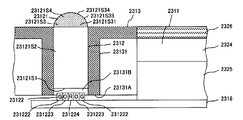
- FIG. 4 is an enlarged cross-sectional view taken along the line VV in FIG. Panel 2314, power circuit 2315, I / O circuit board 2316, control circuit board 2317, display circuit board 2318, connectors 2319, 2320, 2321, 2322, 2323, liquid crystal display panel 2324, liquid crystal display panel backlight 2325, transparent A window plate 2326 and a hinge 2327 are provided.
- the front panel 2313 constitutes the front panel of the control unit 23, and is formed of a light-impermeable resin or the like.
- the back panel 2314 is formed of resin or the like, and the load state detection sensor 21, the contactor 22 and the like built in the control unit 23 are disposed on the back side thereof.
- the power supply circuit unit 2315 is a power supply circuit that supplies DC power to the substrates 2316, 2317, and 2318.
- the power supply circuit unit 2315 takes in AC that has been stepped down to a predetermined voltage by a step-down transformer (not shown), and incorporates a built-in bridge circuit (AC / DC conversion). Circuit) converts the alternating current into direct current, and then smoothes the direct current output of the bridge circuit with a built-in smoothing capacitor such as an electrolytic capacitor, and supplies the smoothed direct current to the substrates 2316, 2317, and 2318. To do.
- the I / O circuit board 2316 is a board on which a so-called input / output circuit is formed, and a load state information signal (analog signal) detected by the load state detection sensor is input to the control circuit board 2317.
- the load state information signal is output.
- the control circuit board 2317 outputs display control signals necessary for the display devices 2311 and 2312 to the load status monitoring screen display device 2311 and the abnormality display device 2312 based on the input digital load status information signal. is there.
- the display circuit board 2318 receives the display control signal from the control circuit board 2317, and based on the display control signal, the display operation signal of the ON, the OFF, the abnormal load state, the operation error, It outputs to the abnormality display device 2312 and outputs a display operation signal such as a measured value of the load state to the load state monitoring screen display device 2311.
- the connector 2319 connects the detection output signal line of the load state detection sensor 21 and the input terminal of the I / O circuit board 2316.
- the connectors 2320 and 2321 connect the output terminal of the I / O circuit board 2316 and the input terminal of the control circuit board 2317, and connect the input / output terminals of both boards without using a harness. Therefore, it is also called a board-to-board connector.
- the connector 2322 is a terminal that is provided in the power supply circuit unit 2315 and takes in an AC power supply (secondary output of a step-down transformer not shown).
- the connector 2323 connects the output terminal of the control circuit board 2317 and the input terminal of the display circuit board 2318, and is the board-to-board connector.
- the liquid crystal display panel 2324 is a display panel using liquid crystal, and displays the measured value of the load state and the like based on a display operation signal from the display circuit board 2318.
- the backlight 2325 of the liquid crystal display panel is a light source that emits light toward the liquid crystal display panel 2324 from the back side of the liquid crystal display panel 2324, and makes the display of the liquid crystal display panel 2324 clear. It should be noted that the light intensity of the backlight 2325 and / or the background color of the liquid crystal display panel 2324 is brighter in the event of an abnormality than in the steady state of the motor load based on the display operation signal from the display circuit board 2318. This makes it easier to visually recognize even a large number of rows.
- the transparent window plate 2326 protects the front surface of the liquid crystal display panel 2324, and is attached to the opening of the front panel 2313.
- the hinge 2327 is provided in the fixing portion 2328, and both the one end 2313A on the back surface side of the front panel 2313 and the one end 2314A on the same side as the one end 2313A of the front panel 2313 of the back panel 2314 are pivotally attached.
- both the front panel 2313 and the back panel 2314 can be rotated individually in the direction of the arrow A about the hinge 2327 as an axis, that is, can be opened and closed with one opening.
- the front panel 2313 When the front panel 2313 is rotated (opened) about the hinge 2327 in the direction of arrow A, the front panel 2313, the display lens 23121, and the transparent window plate 2326 are centered on the hinge 2327.
- the power supply circuit unit 2315, the I / O circuit board 2316, the control circuit board 2317, and the display circuit which are rotated and opened integrally in the direction of the arrow A, and as a result are exposed to the outside.
- Maintenance inspection of the substrate 2318, the connectors 2319, 2320, 2321, 2322, 2323, the liquid crystal display panel 2324, the backlight 2325 of the liquid crystal display panel, and the like can be performed.
- the back panel 2314 when the back panel 2314 is rotated (opened) in the direction of arrow A1 with the hinge 2327 as an axis, the back panel 2314, the power supply circuit unit 2315, the I / O circuit board 2316, and the control circuit board 2317.
- the display circuit board 2318, the connectors 2319, 2320, 2321, 2322, 2323, the liquid crystal display panel 2324, the backlight 2325 of the liquid crystal display panel, and the hinge 2327 are integrated in the direction of the arrow A2.
- the load state detection sensor 21 and the contactor 22 that have been exposed to the outside as a result of being rotated and opened can be inspected for maintenance.
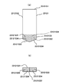
- FIG. 6 is an enlarged cross-sectional view showing the portion of the abnormality display device 2312 in FIG. 5 further enlarged
- FIG. 7 is an external view of the portion surrounding the light transmission portion of the lens 23121
- FIG. 9 is a perspective view of the lenses 23121, 231211, 231212, 231213, and 231214.
- the liquid crystal display is positioned at a predetermined distance from the liquid crystal display panel 2324, the backlight 2325 of the liquid crystal display panel, and the transparent window plate 2326 in the vicinity of the load state monitoring screen display device 2311 of the front panel 2313.
- a cylindrical portion 23131 that integrally protrudes from the front panel 2313 to the back side is formed in parallel with the stacking direction of the panel 2324, the backlight 2325 of the liquid crystal display panel, and the transparent window plate 2326.
- the cylindrical portion 23131 has four (that is, a plurality of) lens mounting through holes 231111, 231312, 231313, and 231314 that penetrate from the rear surface side of the front panel 2313 to the front surface side and extend in parallel with each other. Is provided.
- Each of these lens mounting through holes 231111, 2331312, 231313, and 231314 has a rectangular shape such as a rectangle as shown in the drawing, and the sizes thereof are the same.
- the cylindrical portion 23131 can be said to have a plurality of lens mounting through holes 231311, 2331312, 231313, and 231314 that pass through the front panel 2313 in the front-rear direction.
- the cylindrical portion having the mounting through hole 233131, the cylindrical portion having the lens mounting through hole 2331312, the cylindrical portion having the lens mounting through hole 231313, and the cylindrical portion having the lens mounting through hole 231314 are integrated. It can also be said that the formed cylindrical portion.
- the ON display lens 231211 is displayed in the lens mounting through-hole 2331311, the OFF display lens 231212 is displayed in the lens mounting through-hole 233131, and the abnormality in the load state is displayed in the lens mounting through-hole 231313.
- the lens 231213 for displaying the operation error is inserted into the lens mounting through-hole 231314, and is fixed in the corresponding lens mounting through-hole.
- the light receiving surfaces 23121S1 of the lenses 231211, 231212, 231213, and 231214 are positioned on the front side of the inner end surface 23131A of the cylindrical portion 23131, and the lenses 231211, 231212, 231213, and 231214 A recess 23131B is formed between each light receiving surface 23121S1 and the inner end surface 23131A of the cylindrical portion 23131.
- the light source 23122 includes an ON display LED 231221 facing the ON display lens 231211, an OFF display LED 231222 facing the OFF display lens 231212, and a load condition abnormality display lens 231213. It is composed of an LED 231223 for displaying an abnormal load state and an LED 231224 for displaying an in-unit operation error facing a lens 231214 for displaying an in-unit operation error.
- the ON display LED 231221 is composed of three LEDs of green G, red R, and green G arranged at predetermined intervals, and the OFF display LED 231222 is arranged at predetermined intervals. It consists of three LEDs of green G, red R, and green G, and the LED 231223 for displaying the load condition abnormality is composed of two LEDs of orange O arranged at a predetermined interval, and the operation error display in the unit
- the red LED 231224 is composed of one red R LED.
- the red R LED 231224 for displaying the in-unit operation error emits light in response to a display drive signal from the display circuit board 2318.
- the LED 231221 for ON display has a light emitting surface 23122A at the front end located in the recess 23131B corresponding to the lens 231211 for opposing ON, and the LED 231222 for OFF display is opposed to the opposing OFF
- the front light emitting surface 23122A is located in the recess 23131B corresponding to the display lens 231212, and the load state abnormality display LED 231223 is opposed to the load state abnormality display lens 231213.
- the front light emitting surface 23122A is located in the corresponding recess 23131B, and the LED 231224 for displaying the in-unit operation error is opposite to the indenting 23231B corresponding to the lens 231214 for displaying the in-unit operation error.
- the front light emitting surface 23122A is located inside. That is, the light emitting surface 23122A on the front side of the light source 23122 is located in the light-impermeable cylindrical portion 23131, and the diffusion of light emitted from the light emitting surface 23122A is diffused by the cylindrical portion 23131. As a structure to be prevented.
- a gap g of a predetermined length is secured between the light emitting surface 23122A of the light source 23122 and the light receiving surface 23121S1 of the display lens 23121, and the light emitting surface 23122A of the light source 23122 and the display
- the lens 23121 has a structure that prevents the light receiving surface 23121S1 from coming into contact with the lens 23121.
- the display lens 23121 that is, the ON display lens 231211, the OFF display lens 231212, the load state abnormality display lens 231213, and the operation error display lens 231214
- a columnar light transmission portion 23121S2 that transmits the light incident from the light source 23122 to the light receiving surface 23121S1, and a light emission portion 23121S3 that protrudes outside from the front panel 2313 and emits the light transmitted by the light transmission portion 23121S2.
- the light emitting portion 23121S3 has a substantially flat first side surface 23121S31 having a substantially arched tip portion, and is substantially parallel to the first side surface 23121S31 and has a substantially arched shape.
- the first side surface 23121S31, the second side surface 23121S32, and the front surface 23121S33 are all roughened 23121S34.
- the roughening process is a so-called roughening process such as a texture process, a file (sandpaper) process, or a surface process using a laser.
- the light emitting portion 23121S3 includes a first flat side surface 23121S31 having a substantially arch-shaped tip portion, and substantially parallel to the first side surface 23121S31 and a tip portion having a substantially arched shape.
- a substantially flat second side surface 23121S32, and a front surface 23121S33 extending substantially in an arch shape across the peripheral edge portion of the first side surface 23121S31 and the peripheral edge portion of the second side surface 23121S32,
- the directions of arrows a, b, c, d, e that is, from above
- the light emitted from the light emitting unit 23121S3 is strong, whether viewed from below, viewed from the left or right, or viewed from the front.
- the light emitting unit 23121S3 is hemispherical. Compared with the case where the entire surface is roughened, the visibility is better. It was. Therefore, in a large control center (see FIG. 2) composed of a large number of rows for monitoring and controlling the load states of a large number of motor loads, the control units 23, 23,.
- the anomaly display device 2312 can be viewed from a relatively distant position such as the factory passage AA without the observer approaching the line and checking it visually.
- Embodiment 2 As a second embodiment of the present invention, various LED arrangements are illustrated in FIG.
- any of the ON display LED 231221, the OFF display LED 231222, the load state abnormality display LED 231223, and the in-unit operation error display LED 231224 described in the first embodiment is limited to the arrangement illustrated in the first embodiment. It is possible to use various arrangements as illustrated in FIGS. 10A to 10E.
- G is a green light emitting LED
- R is a red light emitting LED
- the luminance increases as the number of lenses increases with respect to one lens, and each roughened surface shown in the first embodiment. Visibility from all directions due to the emitted light at is improved.
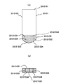
- Embodiment 3 FIG.
- the shape is a trapezoidal pentagon (the tip is triangular), and the planar shape of the front surface 23121S33 extending across the peripheral edge of the first side surface 23121S31 and the peripheral edge of the second side surface 23121S32 is also included.
- This is an example of a trapezoidal pentagon (the shape of the tip is a triangle) in accordance with the planar shape of the first side surface 23121S31 and the second side surface 23121S32.
- Embodiment 4 FIG.
- the shape is a trapezoidal hexagon (the shape of the tip is a quadrangle), and the planar shape of the front surface 23121S33 extending across the peripheral edge of the first side surface 23121S31 and the peripheral edge of the second side surface 23121S32 is also available.
- This is an example of a trapezoidal hexagon (the shape of the tip is a quadrangle) in accordance with the planar shape of the first side surface 23121S31 and the second side surface 23121S32.
- the control units 23, 23, in a large control center (see FIG. 2) composed of a large number of rows for monitoring and controlling the load states of a large number of motor loads, the control units 23, 23,.
- the anomaly display device 2312 can be viewed from a relatively distant position such as the factory passage AA without the observer approaching the line and checking it visually.
- planar shape is trapezoidal pentagon (tip shape is triangular), and planar shape is trapezoidal. And the hexagon (the shape of the tip portion is a quadrangle)).
- a load state monitoring screen display device for displaying a load state and an abnormality display device located in the vicinity of the load state monitoring screen display device are provided on the front panel of the control unit constituting each of the plurality of rows.
- the abnormality display device includes a light source disposed inside the front panel, a light receiving surface that passes through the front panel and receives light generated by the light source, and a columnar light transmission that transmits light incident on the light receiving surface.
- the light emitting portion includes a substantially flat first side surface having a substantially arch-shaped tip portion, a substantially flat second side surface substantially parallel to the first side surface and a substantially arch-shaped tip portion, and the first side surface.
- a front surface extending substantially in an arch shape across a peripheral edge portion of one side surface and a peripheral edge portion of the second side surface, and any one of the first side surface, the second side surface, and the front surface
- the control center is also characterized by being roughened.
- Feature point 2 In the control center described in feature point 1, at least two pairs of the lens and the light source are provided, one pair displays an abnormal load state, and the other pair operates in the control unit. A control center that displays errors.
- Feature point 3 The control center according to feature point 2, wherein each pair of lenses is juxtaposed and each pair of light sources is juxtaposed.
- Feature point 4 In the control center according to any one of feature points 1 to 3, the lens is mounted in a lens mounting through-hole provided in the front panel, and the load state is provided in the control unit.
- Feature point 5 In the control center according to any one of feature points 1 to 4, at least a portion of the front panel surrounding the light transmission portion is formed of a light-impermeable resin, and the lens is a light-transmissive plastic. A control center, wherein the light source is an LED.
- Feature point 6 In the control center according to feature point 4 or feature point 5, the lens mounting through-hole is formed in a cylindrical portion integrally provided in the front panel, and the front surface is located in front of the inner end surface of the cylindrical portion.
- the control center wherein the light receiving surface of the lens is located on the side, and a light emitting surface on the front side of the light source is located in the cylindrical portion.
- Feature point 7 The control center according to feature point 6, wherein a gap having a predetermined length is formed between the light receiving surface of the lens and the light emitting surface of the light source.
- Feature point 8 The control center according to any one of feature points 4 to 7, wherein the front panel is pivotable with respect to the display control board.
- Feature point 9 A control center characterized in that each control unit of each row has at least one feature configuration of the feature points 1 to 8.
Landscapes
- Physics & Mathematics (AREA)
- General Physics & Mathematics (AREA)
- Optics & Photonics (AREA)
- Illuminated Signs And Luminous Advertising (AREA)
- Devices For Indicating Variable Information By Combining Individual Elements (AREA)
- Arrangement Of Elements, Cooling, Sealing, Or The Like Of Lighting Devices (AREA)
Priority Applications (3)
| Application Number | Priority Date | Filing Date | Title |
|---|---|---|---|
| JP2009553330A JP5008729B2 (ja) | 2008-02-14 | 2008-07-14 | コントロールセンタ |
| KR1020107020077A KR101193253B1 (ko) | 2008-02-14 | 2008-07-14 | 컨트롤 센터 |
| CN200880126904.1A CN101953042B (zh) | 2008-02-14 | 2008-07-14 | 控制中心 |
Applications Claiming Priority (2)
| Application Number | Priority Date | Filing Date | Title |
|---|---|---|---|
| JP2008033229 | 2008-02-14 | ||
| JP2008-033229 | 2008-02-14 |
Publications (1)
| Publication Number | Publication Date |
|---|---|
| WO2009101716A1 true WO2009101716A1 (ja) | 2009-08-20 |
Family
ID=40956760
Family Applications (1)
| Application Number | Title | Priority Date | Filing Date |
|---|---|---|---|
| PCT/JP2008/062697 Ceased WO2009101716A1 (ja) | 2008-02-14 | 2008-07-14 | コントロールセンタ |
Country Status (5)
| Country | Link |
|---|---|
| JP (1) | JP5008729B2 (https=) |
| KR (1) | KR101193253B1 (https=) |
| CN (1) | CN101953042B (https=) |
| TW (1) | TW200935695A (https=) |
| WO (1) | WO2009101716A1 (https=) |
Cited By (2)
| Publication number | Priority date | Publication date | Assignee | Title |
|---|---|---|---|---|
| WO2013005151A1 (en) * | 2011-07-05 | 2013-01-10 | Koninklijke Philips Electronics N.V. | Lighting module |
| EP3340406A4 (en) * | 2015-08-18 | 2019-04-24 | Mitsubishi Electric Corporation | DISPLAY CONTROL SYSTEM AND CONTROL CENTER THEREFOR, SPECIFIC POSITIONNAVIGATION SYSTEM AND CONSOLE INFORMATION DISPLAY SYSTEM |
Citations (10)
| Publication number | Priority date | Publication date | Assignee | Title |
|---|---|---|---|---|
| JPS58155712U (ja) * | 1982-04-14 | 1983-10-18 | カシオ計算機株式会社 | 表示素子取付構造 |
| JPS6168437U (https=) * | 1984-10-12 | 1986-05-10 | ||
| JPS6336105U (https=) * | 1986-08-25 | 1988-03-08 | ||
| JPS63102122A (ja) * | 1986-10-17 | 1988-05-07 | 松下電器産業株式会社 | 照光式パネル |
| JPH01176327U (https=) * | 1988-06-02 | 1989-12-15 | ||
| JPH03138733A (ja) * | 1989-10-25 | 1991-06-13 | Mitsubishi Electric Corp | 動作エラー表示付制御装置 |
| JPH075425A (ja) * | 1993-06-14 | 1995-01-10 | Mitsubishi Electric Corp | モータコントローラ |
| JPH0756528A (ja) * | 1993-08-17 | 1995-03-03 | Mitsubishi Electric Corp | 表示装置 |
| JP2000348517A (ja) * | 1999-06-07 | 2000-12-15 | Stanley Electric Co Ltd | 発光装置 |
| JP2004230563A (ja) * | 2003-01-28 | 2004-08-19 | Nippon Seiki Co Ltd | 樹脂成形品 |
Family Cites Families (4)
| Publication number | Priority date | Publication date | Assignee | Title |
|---|---|---|---|---|
| JPS58155712A (ja) * | 1982-03-12 | 1983-09-16 | Hitachi Ltd | モ−ルド点火コイル |
| US4538002A (en) * | 1984-09-10 | 1985-08-27 | The Goodyear Tire & Rubber Company | Process for the production of hydroxyanisole and alkylated hydroxyanisoles |
| JPS6336105A (ja) * | 1986-07-30 | 1988-02-16 | Nippon Kokan Kk <Nkk> | 膜厚測定装置 |
| JPH01176327A (ja) * | 1987-12-29 | 1989-07-12 | Matsushita Electric Ind Co Ltd | 垂直磁気記録媒体の製造方法 |
-
2008
- 2008-07-14 CN CN200880126904.1A patent/CN101953042B/zh active Active
- 2008-07-14 WO PCT/JP2008/062697 patent/WO2009101716A1/ja not_active Ceased
- 2008-07-14 JP JP2009553330A patent/JP5008729B2/ja active Active
- 2008-07-14 KR KR1020107020077A patent/KR101193253B1/ko active Active
- 2008-07-21 TW TW97127590A patent/TW200935695A/zh not_active IP Right Cessation
Patent Citations (10)
| Publication number | Priority date | Publication date | Assignee | Title |
|---|---|---|---|---|
| JPS58155712U (ja) * | 1982-04-14 | 1983-10-18 | カシオ計算機株式会社 | 表示素子取付構造 |
| JPS6168437U (https=) * | 1984-10-12 | 1986-05-10 | ||
| JPS6336105U (https=) * | 1986-08-25 | 1988-03-08 | ||
| JPS63102122A (ja) * | 1986-10-17 | 1988-05-07 | 松下電器産業株式会社 | 照光式パネル |
| JPH01176327U (https=) * | 1988-06-02 | 1989-12-15 | ||
| JPH03138733A (ja) * | 1989-10-25 | 1991-06-13 | Mitsubishi Electric Corp | 動作エラー表示付制御装置 |
| JPH075425A (ja) * | 1993-06-14 | 1995-01-10 | Mitsubishi Electric Corp | モータコントローラ |
| JPH0756528A (ja) * | 1993-08-17 | 1995-03-03 | Mitsubishi Electric Corp | 表示装置 |
| JP2000348517A (ja) * | 1999-06-07 | 2000-12-15 | Stanley Electric Co Ltd | 発光装置 |
| JP2004230563A (ja) * | 2003-01-28 | 2004-08-19 | Nippon Seiki Co Ltd | 樹脂成形品 |
Cited By (2)
| Publication number | Priority date | Publication date | Assignee | Title |
|---|---|---|---|---|
| WO2013005151A1 (en) * | 2011-07-05 | 2013-01-10 | Koninklijke Philips Electronics N.V. | Lighting module |
| EP3340406A4 (en) * | 2015-08-18 | 2019-04-24 | Mitsubishi Electric Corporation | DISPLAY CONTROL SYSTEM AND CONTROL CENTER THEREFOR, SPECIFIC POSITIONNAVIGATION SYSTEM AND CONSOLE INFORMATION DISPLAY SYSTEM |
Also Published As
| Publication number | Publication date |
|---|---|
| JPWO2009101716A1 (ja) | 2011-06-02 |
| KR101193253B1 (ko) | 2012-10-19 |
| CN101953042A (zh) | 2011-01-19 |
| TWI376854B (https=) | 2012-11-11 |
| KR20100107526A (ko) | 2010-10-05 |
| TW200935695A (en) | 2009-08-16 |
| JP5008729B2 (ja) | 2012-08-22 |
| CN101953042B (zh) | 2016-11-02 |
Similar Documents
| Publication | Publication Date | Title |
|---|---|---|
| JP5374267B2 (ja) | Led光源ユニット、面状照明装置及び看板 | |
| CN103576380B (zh) | 液晶显示装置 | |
| JP3940721B2 (ja) | 液晶表示装置のled背面照明輝度感知システム | |
| KR102573208B1 (ko) | 표시패널 | |
| US7619881B1 (en) | Display component modules | |
| US10360861B2 (en) | Redundant power/control system for electronic displays | |
| JPWO2010013544A1 (ja) | 照明装置、表示装置、及びテレビ受信装置 | |
| JP5008729B2 (ja) | コントロールセンタ | |
| JP5340442B2 (ja) | コントロールセンタ | |
| US10477676B2 (en) | Display device | |
| JP2010098209A (ja) | 破損発光素子検出システム | |
| JP2014013765A (ja) | Led光源ユニット、面状照明装置及び看板 | |
| RU2626215C1 (ru) | Светосигнальное табло | |
| CN104375296A (zh) | 一种玻璃基板、外围电路板和显示面板 | |
| KR100866064B1 (ko) | 백라이트용 램프 검사장치 | |
| CN222720022U (zh) | Led显示屏 | |
| KR101173662B1 (ko) | Led 검사 장비용 백라이트 유닛 | |
| JP6347467B2 (ja) | テレビ装置 | |
| CN101881660A (zh) | 产品的表面亮度的检测治具及检测方法 | |
| JP2016024333A (ja) | 表示装置 | |
| KR200388570Y1 (ko) | 백라이트 유닛의 광원 검사 장치 | |
| KR20120064780A (ko) | 디스플레이 장치 | |
| JP2006114308A (ja) | 有機elパネル遮光装置、及び有機elパネル検査装置 | |
| CN109975912A (zh) | 显示装置 | |
| TW201641925A (zh) | 載具的發光二極體顯示器 |
Legal Events
| Date | Code | Title | Description |
|---|---|---|---|
| WWE | Wipo information: entry into national phase |
Ref document number: 200880126904.1 Country of ref document: CN |
|
| 121 | Ep: the epo has been informed by wipo that ep was designated in this application |
Ref document number: 08778168 Country of ref document: EP Kind code of ref document: A1 |
|
| WWE | Wipo information: entry into national phase |
Ref document number: 2009553330 Country of ref document: JP |
|
| NENP | Non-entry into the national phase |
Ref country code: DE |
|
| ENP | Entry into the national phase |
Ref document number: 20107020077 Country of ref document: KR Kind code of ref document: A |
|
| 122 | Ep: pct application non-entry in european phase |
Ref document number: 08778168 Country of ref document: EP Kind code of ref document: A1 |