WO2009090893A1 - 容量素子及びこれを備えた半導体装置並びに容量素子の製造方法 - Google Patents
容量素子及びこれを備えた半導体装置並びに容量素子の製造方法 Download PDFInfo
- Publication number
- WO2009090893A1 WO2009090893A1 PCT/JP2009/050023 JP2009050023W WO2009090893A1 WO 2009090893 A1 WO2009090893 A1 WO 2009090893A1 JP 2009050023 W JP2009050023 W JP 2009050023W WO 2009090893 A1 WO2009090893 A1 WO 2009090893A1
- Authority
- WO
- WIPO (PCT)
- Prior art keywords
- insulating film
- lower electrode
- semiconductor device
- capacitive element
- wiring layer
- Prior art date
Links
- 239000004065 semiconductor Substances 0.000 title claims description 60
- 238000000034 method Methods 0.000 title claims description 31
- 238000004519 manufacturing process Methods 0.000 title claims description 18
- 239000010410 layer Substances 0.000 claims abstract description 112
- 239000003990 capacitor Substances 0.000 claims abstract description 53
- 239000011229 interlayer Substances 0.000 claims abstract description 51
- 238000005530 etching Methods 0.000 claims description 23
- 238000009792 diffusion process Methods 0.000 claims description 13
- 230000003647 oxidation Effects 0.000 claims description 11
- 238000007254 oxidation reaction Methods 0.000 claims description 11
- 239000000463 material Substances 0.000 claims description 7
- 229910004298 SiO 2 Inorganic materials 0.000 claims description 4
- BPUBBGLMJRNUCC-UHFFFAOYSA-N oxygen(2-);tantalum(5+) Chemical compound [O-2].[O-2].[O-2].[O-2].[O-2].[Ta+5].[Ta+5] BPUBBGLMJRNUCC-UHFFFAOYSA-N 0.000 claims description 2
- 229910001936 tantalum oxide Inorganic materials 0.000 claims description 2
- 239000007772 electrode material Substances 0.000 abstract description 4
- 239000010949 copper Substances 0.000 description 98
- 238000006243 chemical reaction Methods 0.000 description 18
- 230000008569 process Effects 0.000 description 18
- RYGMFSIKBFXOCR-UHFFFAOYSA-N Copper Chemical compound [Cu] RYGMFSIKBFXOCR-UHFFFAOYSA-N 0.000 description 15
- 229910052802 copper Inorganic materials 0.000 description 15
- 230000003071 parasitic effect Effects 0.000 description 15
- 229910052751 metal Inorganic materials 0.000 description 13
- 239000002184 metal Substances 0.000 description 11
- 238000005516 engineering process Methods 0.000 description 10
- 230000001965 increasing effect Effects 0.000 description 10
- 238000010586 diagram Methods 0.000 description 8
- 230000004888 barrier function Effects 0.000 description 6
- 230000006870 function Effects 0.000 description 6
- 230000006872 improvement Effects 0.000 description 6
- 230000009467 reduction Effects 0.000 description 6
- 239000000758 substrate Substances 0.000 description 5
- 229910052581 Si3N4 Inorganic materials 0.000 description 4
- 238000005229 chemical vapour deposition Methods 0.000 description 4
- HQVNEWCFYHHQES-UHFFFAOYSA-N silicon nitride Chemical compound N12[Si]34N5[Si]62N3[Si]51N64 HQVNEWCFYHHQES-UHFFFAOYSA-N 0.000 description 4
- XUIMIQQOPSSXEZ-UHFFFAOYSA-N Silicon Chemical compound [Si] XUIMIQQOPSSXEZ-UHFFFAOYSA-N 0.000 description 3
- 238000001459 lithography Methods 0.000 description 3
- 238000005498 polishing Methods 0.000 description 3
- 230000004044 response Effects 0.000 description 3
- 229910052710 silicon Inorganic materials 0.000 description 3
- 239000010703 silicon Substances 0.000 description 3
- HBMJWWWQQXIZIP-UHFFFAOYSA-N silicon carbide Chemical compound [Si+]#[C-] HBMJWWWQQXIZIP-UHFFFAOYSA-N 0.000 description 3
- 229910010271 silicon carbide Inorganic materials 0.000 description 3
- 239000000956 alloy Substances 0.000 description 2
- 229910045601 alloy Inorganic materials 0.000 description 2
- 238000004380 ashing Methods 0.000 description 2
- QVGXLLKOCUKJST-UHFFFAOYSA-N atomic oxygen Chemical compound [O] QVGXLLKOCUKJST-UHFFFAOYSA-N 0.000 description 2
- 230000015572 biosynthetic process Effects 0.000 description 2
- 230000007423 decrease Effects 0.000 description 2
- 230000000694 effects Effects 0.000 description 2
- 230000001939 inductive effect Effects 0.000 description 2
- 230000010354 integration Effects 0.000 description 2
- 229910044991 metal oxide Inorganic materials 0.000 description 2
- 150000004706 metal oxides Chemical class 0.000 description 2
- 150000004767 nitrides Chemical class 0.000 description 2
- 230000001590 oxidative effect Effects 0.000 description 2
- 229910052760 oxygen Inorganic materials 0.000 description 2
- 239000001301 oxygen Substances 0.000 description 2
- 238000000059 patterning Methods 0.000 description 2
- 229920002120 photoresistant polymer Polymers 0.000 description 2
- 239000003870 refractory metal Substances 0.000 description 2
- 238000004544 sputter deposition Methods 0.000 description 2
- 229910052715 tantalum Inorganic materials 0.000 description 2
- ATJFFYVFTNAWJD-UHFFFAOYSA-N Tin Chemical compound [Sn] ATJFFYVFTNAWJD-UHFFFAOYSA-N 0.000 description 1
- 230000003064 anti-oxidating effect Effects 0.000 description 1
- 239000003963 antioxidant agent Substances 0.000 description 1
- 230000003078 antioxidant effect Effects 0.000 description 1
- 230000008859 change Effects 0.000 description 1
- 238000003486 chemical etching Methods 0.000 description 1
- 238000004891 communication Methods 0.000 description 1
- 230000007547 defect Effects 0.000 description 1
- 238000000151 deposition Methods 0.000 description 1
- 238000001312 dry etching Methods 0.000 description 1
- 230000009977 dual effect Effects 0.000 description 1
- 238000010438 heat treatment Methods 0.000 description 1
- 238000009434 installation Methods 0.000 description 1
- 238000009413 insulation Methods 0.000 description 1
- 230000007246 mechanism Effects 0.000 description 1
- 230000035515 penetration Effects 0.000 description 1
- 230000002093 peripheral effect Effects 0.000 description 1
- 238000000206 photolithography Methods 0.000 description 1
- 230000000704 physical effect Effects 0.000 description 1
- 238000005268 plasma chemical vapour deposition Methods 0.000 description 1
- 239000002994 raw material Substances 0.000 description 1
- 238000005546 reactive sputtering Methods 0.000 description 1
- 230000004043 responsiveness Effects 0.000 description 1
- 238000003860 storage Methods 0.000 description 1
- 238000001947 vapour-phase growth Methods 0.000 description 1
Images


Classifications
-
- H—ELECTRICITY
- H01—ELECTRIC ELEMENTS
- H01L—SEMICONDUCTOR DEVICES NOT COVERED BY CLASS H10
- H01L27/00—Devices consisting of a plurality of semiconductor or other solid-state components formed in or on a common substrate
- H01L27/02—Devices consisting of a plurality of semiconductor or other solid-state components formed in or on a common substrate including semiconductor components specially adapted for rectifying, oscillating, amplifying or switching and having potential barriers; including integrated passive circuit elements having potential barriers
- H01L27/04—Devices consisting of a plurality of semiconductor or other solid-state components formed in or on a common substrate including semiconductor components specially adapted for rectifying, oscillating, amplifying or switching and having potential barriers; including integrated passive circuit elements having potential barriers the substrate being a semiconductor body
- H01L27/06—Devices consisting of a plurality of semiconductor or other solid-state components formed in or on a common substrate including semiconductor components specially adapted for rectifying, oscillating, amplifying or switching and having potential barriers; including integrated passive circuit elements having potential barriers the substrate being a semiconductor body including a plurality of individual components in a non-repetitive configuration
- H01L27/0688—Integrated circuits having a three-dimensional layout
-
- H—ELECTRICITY
- H01—ELECTRIC ELEMENTS
- H01L—SEMICONDUCTOR DEVICES NOT COVERED BY CLASS H10
- H01L23/00—Details of semiconductor or other solid state devices
- H01L23/52—Arrangements for conducting electric current within the device in operation from one component to another, i.e. interconnections, e.g. wires, lead frames
- H01L23/522—Arrangements for conducting electric current within the device in operation from one component to another, i.e. interconnections, e.g. wires, lead frames including external interconnections consisting of a multilayer structure of conductive and insulating layers inseparably formed on the semiconductor body
- H01L23/5222—Capacitive arrangements or effects of, or between wiring layers
- H01L23/5223—Capacitor integral with wiring layers
-
- H—ELECTRICITY
- H01—ELECTRIC ELEMENTS
- H01L—SEMICONDUCTOR DEVICES NOT COVERED BY CLASS H10
- H01L2924/00—Indexing scheme for arrangements or methods for connecting or disconnecting semiconductor or solid-state bodies as covered by H01L24/00
- H01L2924/0001—Technical content checked by a classifier
- H01L2924/0002—Not covered by any one of groups H01L24/00, H01L24/00 and H01L2224/00
Definitions
- the present invention relates to a capacitor element, a semiconductor device including the capacitor element, and a method for manufacturing the capacitor element.
- ultra-high integrated circuits ULSI: Ultra Large Scale Integrated circuits
- design dimensions are constantly being miniaturized to pursue cost reduction, performance improvement, and power consumption reduction. .
- the function is improved by increasing the number of integrated elements by miniaturization, and the cost is reduced by reducing the chip size.
- Such mixed mounting of circuit blocks having different functions can realize not only cost reduction but also additional performance improvement by combining them such as improvement of communication speed. Further, since the operating voltage can be reduced by miniaturization, power consumption of circuit blocks having the same function can be suppressed.
- Such inductive noise can be reduced by lowering the impedance of the circuit.
- power supply fluctuations can be suppressed by adding capacitance to the circuit.
- Such a capacity is called a decoupling capacity.
- a MOS (Metal Oxide Silicon) capacitor obtained when forming a transistor is used as a decoupling capacitor.
- the insulating film thickness of the MOS capacitor is reduced, which causes a problem that the leakage current of the insulating film increases rapidly.
- the noise margin is drastically reduced, the absolute capacitance value is also insufficient, and the chip area tends to increase due to the decoupling capacitance inserted to stabilize the power supply potential.
- a decoupling capacitor using an insulating film having a dielectric constant higher than that of the MOS capacitor in the wiring layer.
- the capacitor can be placed over the transistor on a plane, so that the installation area can be larger than the MOS capacitor. Since the capacitance value in the same area can be increased by increasing the dielectric constant, a large capacitance can be installed in a limited area.
- Measures against noise during high-speed operation need to consider not only capacity but also responsiveness.
- the power supply noise in high-speed operation contains a lot of high-frequency components.
- the capacitive element has a parasitic resistance component of the electrode, and the parasitic resistance component deteriorates the response to noise.
- the operating speed reaches the gigahertz region, the influence of the parasitic resistance of the electrode becomes obvious, and it becomes difficult to sufficiently exhibit the performance of the decoupling capacitance. Therefore, it is necessary to reduce the electrode resistance as much as possible.
- MOS active elements have promoted the use of high-frequency (RF) signal processing circuits as MOS devices. If the RF device can be constructed with a MOS device, improvement in function and cost reduction can be realized by mixing with a digital baseband circuit. The same merit can be enjoyed by mixing analog circuits and digital circuits.
- passive elements such as resistance elements, capacitance elements, and inductors are effectively used. For this reason, it is extremely important to integrate passive elements in addition to the active elements used in the MOS logic.
- the miniaturization of MOS logic is progressed with generations, but such passive elements are not miniaturized even when generations progress because characteristics are determined only by physical properties. For this reason, the relative area of the passive elements in the ULSI chip is increased, which is an impediment to a reduction in chip cost.
- the formation of parasitic capacitance between the electrode and the silicon substrate is also a problem in terms of operating characteristics. Since the miniaturization of ULSI is three-dimensionally reduced due to the structure, the distance between the wiring layer and the silicon substrate becomes closer. At the same time, the parasitic capacitance formed between the electrode and the substrate is increased by increasing the electrode area of the capacitive element relative to the peripheral circuit. In order to solve the above problems, it is desirable to install a capacitive element having a high dielectric constant away from the substrate. That is, it is necessary to provide a capacitive element in the upper wiring layer. Further, the parasitic resistance of the electrode plate cannot be ignored due to the increase in the size relative to the active element. In high frequency operation, if the parasitic resistance of the electrode increases, the response of the capacitive element deteriorates and the desired operation is not exhibited. Therefore, the parasitic resistance in the capacitive element needs to be reduced as much as possible.
- Patent Document 1 discloses a structure in which an insulating film other than silicon nitride or silicon carbide can be used as a capacitor dielectric film.
- This related technology relates to a capacitor structure formed on a multilayer wiring structure having copper wiring. Silicon nitride or silicon carbide is always formed as an anti-oxidation insulating film on the copper wiring. For this reason, in order to form a capacitor on the copper wiring, it is necessary to use these films as a capacitor insulating film.
- This related technique is a technique for avoiding this restriction.
- This related technology is characterized in that a metal film is used as an antioxidant film instead of an insulating film. A barrier metal is inserted between the exposed surface of the copper wiring and the metal film.
- the metal film is formed so as to remain on the copper wiring, and a capacitive insulating film is formed on the metal film. At this time, the portion other than the metal film exposed as the lower electrode on the copper wiring is only exposed to the interlayer insulating film, and the lower electrode has higher oxidation resistance than the copper wiring, so that it is highly oxidizable.
- a metal oxide dielectric film or the like can be used as a capacitive insulating film.
- Patent Document 2 discloses a structure that uses Cu wiring as a lower electrode.
- the Cu wiring structure is connected to the lower surface of the lower electrode made of a material that prevents Cu diffusion, so that electric charges are supplied to the lower electrode through the Cu wiring, and oxidation of the interlayer insulating film or the like is performed.
- a structure capable of preventing Cu diffusion into the film is provided.
- the lower electrode and the barrier metal are inserted between the upper and lower wirings even in the portion where no capacitance is formed.
- the lower electrode material and barrier metal having strong oxidation resistance generally have high electric resistance, and increase resistance between the upper and lower wirings.
- the capacitor insulating film and the upper electrode are formed.
- the insulating film or the like is not uniformly formed between the electrodes, and the characteristics are improved. Defects occur.
- CVD Chemical Vapor Deposition
- the laminated film constituting the capacitive element is patterned inside the opening provided in the insulating film on the lower layer wiring.
- there is a space between the laminated film and the end of the opening (see FIG. 10), and it is necessary to remove this part of the laminated film when the capacitive element is processed by etching.
- the capacitive element having the feature that the parasitic resistance can be reduced by the lower electrode material being in direct contact with the Cu wiring, a structure in which a space exists between the laminated film and the opening end in the second related technology.
- the space portion becomes a copper wiring, and thus copper diffuses into the laminated film, thereby reducing the reliability of the capacitive element.
- an object of the present invention is to provide a structure that improves the reliability in a capacitive element having a structure in which the lower electrode material is in direct contact with the Cu wiring.
- a capacitive element according to the present invention includes an interlayer insulating film having a first lower electrode made of a Cu wiring layer and an opening having a size provided on the first lower electrode and enclosing the first lower electrode. And a laminate provided in order of the second lower electrode, the capacitive insulating film and the upper electrode on the first lower electrode and the interlayer insulating film so as to contain the opening.
- the opening of the interlayer insulating film in which the capacitor element stack is provided is sized so as to include the first lower electrode, so that the Cu component of the first lower electrode is opened when the opening is formed. Since the second lower electrode is in direct contact with the first lower electrode made of the Cu wiring layer, the reliability can be greatly improved in the structure in which the parasitic resistance can be reduced.
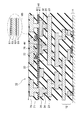
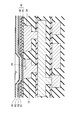
- FIG. 1 is a cross-sectional view showing a capacitive element and a semiconductor device according to the first embodiment of the present invention.
- description will be given based on this drawing.
- the semiconductor device 10 of this embodiment includes a CMOS transistor layer 11 and a Cu multilayer wiring layer 12 formed of two or more layers formed above the CMOS transistor layer 11.
- an arbitrary Cu wiring layer is defined as a first Cu wiring layer 23.
- the first Cu wiring layer 23 is connected to the second Cu wiring layer 31 existing on one layer via the first via plug 24 thereon.
- the first Cu wiring layer 23 is connected to the first lower electrode 32 made of Cu of the capacitive element 30 via the via plug 25.
- a capacitive element interlayer insulating film 40 composed of layers is formed.
- the capacitor element interlayer insulating film corresponds to an “interlayer insulating film” in claims, and is hereinafter abbreviated as “capacitor element interlayer film”.
- the capacitive element interlayer 40 is opened, and at least a part of the second lower electrode 61 is in direct contact with the first lower electrode 32.
- the first lower electrode 32 is completely contained in the opening 44 and does not straddle the side wall (circumferential end) of the opening 44.
- the capacitive element 30 is formed with a laminated body 65 composed of the second lower electrode 61, the capacitive insulating film 62, the upper electrode 63, and the etching stopper layer 51 in a shape extending to the opening 44 and the outside thereof.
- Each wiring layer is insulated by an insulating film (reference numeral omitted).
- the capacitive element 30 of the present embodiment includes a first lower electrode 32 made of a Cu wiring layer, and an opening 44 that is provided on the first lower electrode 32 and has a size that encloses the first lower electrode 32.
- a second lower electrode 61, a capacitive insulating film 62, and an upper electrode 63 are provided in this order on the first lower electrode 32 and the capacitive element interlayer film 40 so as to enclose the capacitive element interlayer film 40 and the opening 44.
- a laminated body 65 is provided.
- the second lower electrode 61 and the upper electrode 63 have the same planar shape.
- the opening 44 has a tapered shape with the upper side greatly opening.
- the stacked body 65 also has an etching stop layer 51 provided on the upper electrode 63.
- the semiconductor device 10 of this embodiment includes a first Cu wiring layer 23, a second Cu wiring layer 31 connected to the first Cu wiring layer 23 via a first via plug 24, and a capacitive element. 30.
- the first lower electrode 32 is a Cu wiring layer formed in the same layer as the second Cu wiring layer 31, and is connected to the first Cu wiring layer 23 via the via plug 25.
- the semiconductor device 10 includes a third Cu wiring layer 75 connected to the second Cu wiring layer 31 via a second via plug 71 at the upper side.
- the upper electrode 63 is connected to the third Cu wiring layer 76 through a contact plug 72 formed in the same layer as the second via plug 71.
- the capacitor element interlayer film 40 is composed of a wiring cap insulating film 41 having a property of preventing oxidation of the Cu wiring layer and diffusion of Cu element, and a material different from the wiring cap insulating film 41 provided on the wiring cap insulating film 41. It has two layers with the hard mask insulating film 42.
- the wiring cap insulating film 41 is made of SiCN or SiC
- the hard mask insulating film 42 is made of SiO 2 or SiCOH.
- the capacitor insulating film 62 is made of, for example, SiN having a thickness of 5 nm or more, or made of tantalum oxide formed by a plasma oxidation method.
- the capacitive element 30 covers the surface of the first lower electrode 32 formed at the same time as the optional second Cu wiring layer 31 and the second Cu wiring layer 31 and the first lower electrode 32.
- a capacitive element interlayer film 40 having an enclosing opening 44, a second lower electrode 61, a capacitive insulating film 62, and an upper part formed so as to enclose the opening 44 and extend on the capacitive element interlayer film 40.
- a stacked body 65 including an electrode 63 and an etching stopper layer 51 is provided.
- the first lower electrode 32 is connected to the lower first wiring layer 23 via the via plug 25, and the upper electrode 63 is connected to the upper third electrode via the contact plug 72. Are connected to the wiring layer 76.
- a capacitor element interlayer film 40 is formed on the second Cu wiring layer 31 and the first lower electrode 32, and an opening 44 is provided in the capacitor element interlayer film 40 so as to enclose the first lower electrode 32 in a plane. Further, the capacitive element 30 is formed so as to include the opening 44 in a plane.
- the first lower electrode 32 made of the Cu wiring layer is completely covered with either the second lower electrode 61 or the capacitor element interlayer film 40 that prevents diffusion of Cu. Further, since the second lower electrode 61 is in direct contact with the first lower electrode 32 made of the Cu wiring layer, it is possible to reduce the parasitic resistance.
- the Cu wiring layer is used as the first lower electrode 32, it is possible to reduce the thickness of the entire capacitive element 30, and to ensure scaling in a semiconductor process in which miniaturization proceeds.
- the side wall of the opening 44 is not located on the first lower electrode 32 made of the Cu wiring layer, the reliability of the capacitor 30 is improved as will be described later.
- the lithography process for opening the capacitor element interlayer film 44 alignment using a mark formed by a lower Cu wiring through the optically transparent capacitor element interlayer film 44 is possible. Therefore, by simultaneously forming the mark for alignment when patterning the capacitive element 30 in this opening process, the capacitive element 30 can be mounted on the semiconductor device 10 by adding lithography twice in total.
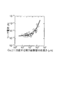
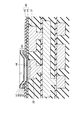
- FIG. 2 is a graph for explaining the effects of the semiconductor device and the capacitive element in the present embodiment. Hereinafter, a description will be given based on FIG. 1 and FIG.
- the side wall of the opening 44 is not located on the first lower electrode 32 made of the Cu wiring layer, that is, the opening 44 is sized to include the first lower electrode 32. It is characterized by that. This is because it has been confirmed that the reliability deteriorates when the side wall of the opening 44 is positioned on the first lower electrode 32. This will be described in detail below.
- FIG. 2 shows the result of investigating the relationship between the total length of the side wall of the opening 44 and the leakage current of the capacitive element 30 in the structure in which the side wall of the opening 44 exists on the first lower electrode 32 made of the Cu wiring layer.
- the size of each capacitive element 30 is the same for the stacked body 65 and the first lower electrode 32, and only the size of the opening 44 is different.
- the leakage current tends to increase as the total length of the side wall of the opening 44 increases. This is considered to be because Cu exposed at the bottom of the opening 44 is scattered by being exposed to plasma and adheres to the side wall of the opening 44 when the opening 44 is etched. Since the etching product of Cu has low volatility, chemical etching hardly occurs.
- the physically scattered Cu scattered material reattaches to the side wall of the opening 44.
- Cu attached to the bottom surface of the opening 44 is removed by etching, but Cu attached to the side wall of the opening 44 tends to remain.
- Cu adhering to the side wall of the opening 44 diffuses and reaches the capacitive insulating film 62 and the like, thereby increasing the leakage current of the capacitive element 30.
- the opening 44 is sized to enclose the first lower electrode 32, so that the side wall of the opening 44 is moved away from the first lower electrode 32, and etched Cu scattered objects are opened. Since it is difficult to adhere to the side wall of the portion 44, the reliability is improved.
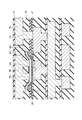
- FIG. 3 to FIG. 9 are cross-sectional views of each process showing a method for manufacturing a capacitive element and a semiconductor device according to the second embodiment of the present invention.
- description will be given based on these drawings.
- This embodiment is a method of manufacturing the capacitive element 30 and the semiconductor device 10 of FIG.
- the uppermost layer of the two or more Cu wiring layers in FIG. 1 is the Cu wiring layer 13, and the lower layers are omitted.
- a film omitted in FIG. 1 is also referred to.
- a wiring cap insulating film 14 for preventing oxidation and diffusion of the Cu wiring is formed.
- a via layer interlayer insulating film 15 is formed, and a first Cu wiring layer 23 and a via plug 16 for connecting to the same are formed by a damascene method.
- a wiring cap insulating film 26 is formed on the Cu wiring layer 23.
- the “via interlayer insulating film” is abbreviated as “via interlayer film”.
- the second Cu wiring layer 31 and the first via plug 24 are formed by the damascene method.
- the first lower electrode 32 is also formed at the same time, and the via plug 25 that connects the capacitive element and the external circuit is formed in the same manner as the first via plug 24.
- a SiN or SiCN film is formed as the wiring cap insulating film 41 for the purpose of preventing Cu oxidation and Cu diffusion, and subsequently, SiO 2 or SiOCH is formed as the hard mask insulating film 42.
- the two layers of the wiring cap insulating film 41 and the hard mask insulating film 42 become the capacitive element interlayer film 40.
- an opening 43 is formed in the hard mask insulating film 42 through a photolithography process and an etching process. At this time, it is important to stop the etching on the wiring cap insulating film 41 using the selective characteristics of dry etching. Further, as shown in the drawing, it is preferable that the end of the opening 43 has a taper shape in order to improve the coverage of a laminate to be formed later.
- the photoresist is removed by ashing. At this time, since the Cu surface of the first lower electrode 32 is not exposed, the oxidation of Cu by oxygen plasma can be suppressed.
- the wiring cap insulating film 42 is etched using the opening 43 of the hard mask insulating film 42 as a mask to form an opening 44 reaching the Cu surface of the first lower electrode 32.
- the end of the opening 44 has a tapered shape in order to improve the coverage of a laminate to be formed later.
- the opening 44 is sized to enclose the first lower electrode 32, so that the side wall 44 a of the opening 44 is moved away from the first lower electrode 32, and etched Cu scattered matter Since it is difficult to adhere to the side wall 44a, the reliability is improved.
- a film that becomes the second lower electrode 61, the capacitor insulating film 62, the upper electrode 63, and the etching stop layer 51 is sequentially formed.
- a refractory metal film such as Ti, Ta, or W, an alloy film containing these metal elements, or a nitride film thereof is used. It is also effective to use a laminated film composed of a plurality of films as any of these films.
- the second lower electrode 61 it is an important property to suppress the diffusion of Cu element.
- the film thickness of the second lower electrode 61 is 5 nm to 30 nm in order to realize the thinning of the capacitive element and suppress the diffusion of Cu element.
- a silicon nitride film having a thickness of 5 nm or more is formed by a plasma CVD method.
- the film thickness of the silicon nitride film is thinner than 5 nm, the insulation property is drastically lowered, so that sufficient reliability cannot be obtained.
- the upper electrode 63 a refractory metal film such as Ti, Ta, or W, an alloy film containing these metal elements, or a nitride film thereof is used. Since the upper electrode 63 is exposed to an etching atmosphere during etching of the upper electrode contact, the film thickness is set to a relatively large value of 20 nm or more for the purpose of preventing penetration.
- the etching stop layer 51 is made of a material such as SiCN or SiN, like the wiring cap insulating film 41.
- the etching stopper layer 51, the upper electrode 63, the capacitor insulating film 62, and the second lower electrode 61 are patterned in this order in a single lithography process so as to include the opening 44 in a plane.
- the laminated body 65 is formed.
- the patterning of the stacked body 65 may be performed by etching the etching stop layer 51 using a photoresist as a mask, and etching the stacked film below the upper electrode 63 using the etching stop layer 51 as a mask after ashing.
- the etching stop layer 51 to the lower metal layer may be collectively etched using a hard mask such as a SiO 2 film. In this case, the apparent wiring cap insulating film 41 remains in the device as a laminated structure with the hard mask insulating film 42.
- the via interlayer film 73 after forming the via interlayer film 73, the uppermost third Cu wiring layers 75 and 76 and the upper electrode 63 of the capacitive element 30 are formed by the single damascene method or the dual damascene method.
- the contact plug 72 and the second via plug 71 for connecting the Cu wiring layers are formed.
- a wiring cap insulating film 77 is formed on the surface including the surfaces of the third Cu wiring layers 75 and 76.
- the via interlayer film that is, the wiring interlayer insulating film itself may have a multi-layer structure due to process requirements. Therefore, the via interlayer film 73 is usually composed of a multilayer insulating film.
- the contact plug 72 to the upper electrode 63 of the capacitive element 30 is shallower than the second via plug 71 between the Cu wiring layers.
- both the contact plug 72 and the second via plug 71 have the wiring cap insulating films 41 and 51 functioning as an etch stopper at the bottom thereof, openings with different depths can be performed without any problem. it can.
- the process of forming the capacitive element interlayer film 40 on the surface including the first lower electrode 32 (FIG. 4) and the etching of the capacitive element interlayer film 40 are performed.
- the step of forming the opening 44 (FIGS. 5 and 6) and the first lower electrode 61 on the capacitor element interlayer film 40 and the first lower electrode 32 in the opening 44 are formed.
- Step of sequentially forming a layer, a second layer that becomes the capacitive insulating film 62, and a third layer that becomes the upper electrode 63 (FIG. 7), and the first layer, the second layer, and the third layer are collectively etched.
- the opening 44 is processed to a size that encloses the first lower electrode 32, the Cu component of the first lower electrode 33 is formed on the side wall of the opening 44 when the opening 44 is formed. Since the second lower electrode 61 is in direct contact with the first lower electrode 32 made of the Cu wiring layer, the reliability can be greatly improved in the structure in which the parasitic resistance can be reduced.
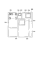
- FIG. 10 shows a semiconductor device according to the third embodiment of the present invention
- FIG. 10 [1] is a circuit diagram of the semiconductor device
- FIG. 10 [2] is a plan view of a capacitive element included in the semiconductor device.
- a semiconductor device 100 in FIG. 10A is a successive approximation AD (Analog to Digital) conversion circuit, and includes a comparator 101, a capacitor array 102, a switch unit 103, and the like.
- AD Analog to Digital
- the capacitance element having a capacitance value C is increased by a factor of 2, such as 1, 2, 4, 8,... Each capacitive element is required.
- a maximum capacity of 2 N-1 C is required, and a total capacity of 2 N C is required.
- FIG. 10 [2] shows a plan configuration diagram of the capacitor array 102.
- Each capacitive element 30 of the capacitive array 102 has the same configuration as the capacitive element 30 shown in FIG.
- One capacitive element 30 includes a first lower electrode 32 formed simultaneously with the second Cu wiring layer, a capacitive element interlayer film having an opening 44 in a shape including the first lower electrode 32 therein, and a laminate. 65.
- the layer above the stacked body 65 is removed and shown.
- the stacked body 65 includes a second lower electrode made of TaN having a thickness of 5 nm to 30 nm, a capacitive insulating film made of SiN having a thickness of 5 nm to 15 nm, an upper electrode made of TiN having a thickness of 20 nm to 100 nm, and etching. Consists of stop layers.
- a second lower electrode made of TaN having a thickness of 5 nm to 30 nm a thickness of 5 nm to 30 nm
- a capacitive insulating film made of SiN having a thickness of 5 nm to 15 nm
- an upper electrode made of TiN having a thickness of 20 nm to 100 nm
- etching etching. Consists of stop layers.
- Consists of stop layers since it is necessary to arrange a very large number of capacitive elements 30, it is important to increase the capacitance per unit area and reduce the capacitance area. For this purpose, it is effective to use TaO
- TaO used as a capacitor insulating film is formed by depositing metal Ta with a thickness of 3 to 7 nm by sputtering and oxidizing it in an oxidizing plasma atmosphere at 350 ° C.
- the film may be formed by reactive sputtering in which oxygen is introduced into the sputtering atmosphere, or a vapor phase growth method such as a CVD method may be used.
- the capacitive element 30 having low parasitic resistance and high reliability since the capacitive element 30 having low parasitic resistance and high reliability is used, the reliability can be improved.
- FIG. 11 and 12 show a semiconductor device according to a fourth embodiment of the present invention
- FIG. 11 [1] is a signal flow diagram
- FIG. 11 [2] is a configuration diagram of a conversion unit in the semiconductor device
- 12 [1] is a circuit diagram of the operational amplifier circuit in the conversion unit
- FIG. 12 [2] is a plan view of the capacitive element in the operational amplifier circuit.
- a semiconductor device 200 shown in FIG. 11 [1] is a pipelined AD converter circuit, which converts a plurality of conversion units 201 for each bit, and a digital signal of a predetermined code from a 1-bit signal output from each conversion unit 201.
- An output code conversion circuit 202 and the like are provided.
- the input analog value is output as a digital signal by one bit from the most significant bit at each stage.
- N-1 conversion units 201 are required for N-bit conversion.
- the semiconductor device 200 has a feature that the next signal processing is started without waiting for the output of all bits. Since the pipeline type AD conversion circuit itself is well known, detailed description of its operation is omitted.
- FIG. 11 [2] shows the configuration of the conversion unit 201 at each stage.
- the conversion unit 201 includes an operational amplifier circuit 210, a sample hold circuit 221, an ADC (Analog-Digital Converter) 222, a DAC (Digital-Analog Converter) 223, and the like.
- a detailed configuration of the operational amplifier circuit 210 is shown in FIG.
- the operational amplifier circuit 210 shown in FIG. 12 [1] uses a switched capacitor including an operational amplifier 211, a capacitor circuit 212, and the like.
- the relative accuracy of the capacitors C1 and C2 is an extremely important factor. The relative accuracy depends on the size of the capacitive element, and the accuracy increases as the size increases.
- FIG. 12 [2] shows the layout of the capacitor element applied to the operational amplifier circuit 210.
- Capacitors C1 and C2 have the same configuration as the capacitive element 30 of FIG. 1, as shown. Capacitors C1 and C2 are adjacent to each other. Since one capacitive element 30 has a relatively large area, the area of the first lower electrode 32 is increased. However, it is difficult to form a continuous large-area pattern for Cu wiring because of its manufacturing problems. Usually, the Cu wiring is formed by removing an excess portion of Cu embedded in the groove portion by polishing by CMP (Chemical-Mechanical Polishing). At this time, if a large area of Cu is used, the polishing rate increases at the center, resulting in a concave shape.
- CMP Chemical-Mechanical Polishing
- the stacked body 65 is formed in a shape that includes the opening 44. In FIG. 12 [2], the layer above the stacked body 65 is removed and shown.
- the capacitive element 30 having low parasitic resistance and high reliability since the capacitive element 30 having low parasitic resistance and high reliability is used, the reliability can be improved.
- FIG. 13 is a plan view showing a semiconductor device according to the fifth embodiment of the present invention. Hereinafter, description will be given based on this drawing.
- the semiconductor device 300 of this embodiment includes an AD conversion circuit 301, a wireless input circuit 302, a PLL circuit 303, a wired input / output circuit 304, a digital circuit 305, and a storage circuit 306 mounted on one chip.
- the AD conversion circuit 301 includes a capacitive element 30a
- the wireless input circuit 302 includes a capacitive element 30b
- the PLL circuit 303 includes a capacitive element 30c
- the digital circuit 305 includes a capacitive element 30d.
- the capacitive elements 30a to 30d have the same configuration as that of the capacitive element 30 in FIG.
- the AD conversion circuit 301 is the same as that described in the third embodiment or the fourth embodiment, and a DA conversion circuit can also be mounted in the same manner.
- the wireless input circuit 302 uses the capacitive element 30b as a pass capacitor for passing a wireless signal from the outside. At this time, since the high frequency response is important, the characteristic of the low parasitic resistance of the capacitive element 30b is extremely effective.
- a circuit that passes only a specific frequency is also mounted, and the capacitive element 30b is also used in that circuit.
- the PLL circuit 303 is for generating a specific frequency, and uses the capacitive element 30c as a loop filter for feeding back a frequency shift.
- the capacitive element 30d works effectively in order to reduce simultaneous switching noise generated when a large number of elements are switched simultaneously.
- the capacitive element is used in various circuits.
- the capacitive elements 30a to 30d according to the present invention can be used for all purposes, and are extremely effective in the semiconductor device 300 having a plurality of functions. It becomes an element.
- the present invention has been described with reference to each of the above embodiments, but the present invention is not limited to each of the above embodiments. Various changes that can be understood by those skilled in the art can be made to the configuration and details of the present invention. Further, the present invention includes a combination of some or all of the configurations of the above-described embodiments as appropriate.
- the present invention relates to a capacitive element incorporated in, for example, an LSI (Large Scale Integrated Circuit), more specifically, a capacitive element composed of a conductive upper electrode film, a capacitive insulating film, and a conductive lower electrode in an LSI having a multilayer wiring. Used.
- LSI Large Scale Integrated Circuit
- FIG. 10 [1] is a circuit diagram of a semiconductor device
- FIG. 10 [2] is a top view of the capacitive element contained in a semiconductor device.
- FIG. 11 [1] is a signal flow figure
- FIG. 11 [1] is a signal flow figure
- FIG. 11 [2] is a block diagram of the conversion part in a semiconductor device.
- the semiconductor device in 4th embodiment of this invention is shown
- FIG. 12 [1] is a circuit diagram of the operational amplifier circuit in a conversion part
- FIG. 12 [2] is a top view of the capacitive element in an operational amplifier circuit. . It is a top view which shows the semiconductor device in 5th embodiment of this invention.
Landscapes
- Engineering & Computer Science (AREA)
- Power Engineering (AREA)
- Physics & Mathematics (AREA)
- Condensed Matter Physics & Semiconductors (AREA)
- General Physics & Mathematics (AREA)
- Computer Hardware Design (AREA)
- Microelectronics & Electronic Packaging (AREA)
- Internal Circuitry In Semiconductor Integrated Circuit Devices (AREA)
- Semiconductor Integrated Circuits (AREA)
Abstract
下部電極材料がCu配線と直接接している構造の容量素子において、信頼性を向上させる構造を提供する。 容量素子(30)は、Cu配線層からなる第一の下部電極(32)と、第一の下部電極(32)上に設けられるととともに第一の下部電極(32)を内包する大きさの開口部(44)を有する容量素子層間膜(40)と、開口部(44)を内包するように第一の下部電極(32)上及び容量素子層間膜(40)上に第二の下部電極(61)、容量絶縁膜(62)及び上部電極(63)の順に設けられた積層体(65)とを備えている。
Description
本発明は、容量素子及びこれを備えた半導体装置並びに容量素子の製造方法に関する。
Si半導体基板上に形成される超高集積回路(ULSI:Ultra Large Scale Integrated circuit)においては、コスト低減、パフォーマンス向上、消費電力低減等を追求するため、設計寸法の微細化が常に進められている。微細化を行って集積される素子数を増大させることで機能の向上を図り、チップサイズを小さくすることでコストの低減を図る。あるいは、集積度の向上によって、異なる機能を有する回路ブロックを複数混載することも可能になり、部品点数を削減することでULSIチップを組み込む装置のコストを低減することも可能になる。このような、異種機能を有する回路ブロックの混載は、コスト削減のみならず、通信速度の向上など、組み合わせることで付加的な性能向上を実現することもできる。また、微細化によって、動作電圧を低減することができるため、同一の機能を持つ回路ブロックの消費電力を抑制することも可能である。
しかし、能動素子の急速な微細化の進展によって、新たな問題が顕在化してきている。以下では、この問題を、電源ノイズ、RF(Radio Frequency)/アナログ、消費電力に分類してまとめる。
まず、電源ノイズについての問題を述べる。微細化が進むことで低電圧化が推し進められるが、集積される素子数が急激に増加するため、消費する電流量は急増する。また、素子の微細化に伴って動作周波数は上昇し続け、スイッチング時間も短縮される。すなわち、スイッチングする際の電流量は増加し、スイッチング時間が短くなるため、電流の時間変化であるdi/dtは急激に大きくなる。この電流の時間変化に回路のインダクタンスLを掛け合わせたL・di/dtは、誘導性の電圧変動であり、同時スイッチングノイズといわれる。同時スイッチングノイズは、電源電位を変動させ、場合によってはロジック状態が反転することがある。上述したように、微細化が進むと、電源電圧が低下することに加え、ノイズによる変動電圧が増大するため、ノイズマージンは加速度的に減少する。
このような誘導性ノイズは、回路のインピーダンスを低下させることで低減することが可能であり、例えば回路に容量を付加することで電源変動を抑制することができる。このような容量をデカップリング容量と呼ぶ。従来のULSIでは、トランジスタを形成するときに得られるMOS(Metal Oxide Silicon)容量をデカップリング容量として用いている。しかし、微細化の進展によってMOS容量の絶縁膜厚は薄膜化し、これにより絶縁膜のリーク電流が急増することが問題となっている。また、ノイズマージンが急激に小さくなっているため、絶対的な容量値も不足してきており、電源電位を安定化するために挿入されるデカップリング容量によってチップ面積が増大する傾向も示している。
以上のような問題点を回避するためには、MOS容量よりも高い誘電率を有する絶縁膜を用いたデカップリング容量を、配線層に用意する必要がある。配線層に容量を組み込むことで、平面上ではトランジスタと重ねて配置することができるため、設置面積をMOS容量よりも大きくとることができる。誘電率を高くすることで、同一面積での容量値を大きくできるので、限られた面積において大きな容量を設置することが可能となる。
高速動作時のノイズ対策については、容量の問題だけではなく、応答性の問題も考える必要がある。高速動作における電源ノイズには高周波成分が多く含まれる。容量素子には電極の寄生抵抗成分が存在しており、その寄生抵抗成分がノイズに対する応答性を劣化させる。動作速度がギガヘルツの領域に達すると、電極の寄生抵抗の影響が顕在化し、デカップリング容量の性能を十分に発揮しにくくなってくる。したがって、電極抵抗を可能な限り低減することが必要となってくる。
MOS能動素子の微細化による動作速度の向上は、高周波(RF)信号処理回路のMOSデバイス化を促進している。RFデバイスをMOSデバイスで構築できれば、デジタルベースバンド回路との混載によって、機能向上、コスト低減などが実現する。アナログ回路とデジタル回路との混載も、同様のメリットを享受できる。RFデバイスやアナログデバイスでは、抵抗素子、容量素子、インダクタなどの受動素子を効果的に利用する。このため、MOSロジックで使用する能動素子に加えて、受動素子を集積化することが極めて重要である。MOSロジックは、世代とともに微細化が進められるが、このような受動素子は、物性のみで特性が決まってしまうために、世代が進んでも微細化しない。このため、ULSIチップにおける受動素子の相対的な面積が増大し、チップコスト低下の阻害要因となっている。
次に、消費電力の側面から見た課題について述べる。微細化技術の進展により、トランジスタの駆動電力が増加することで、チップ内の各デバイスが扱う電流は増加するだけでなく、集積度が向上することでチップ全体で消費される電流は急激に増加することになる。消費電力は、回路内の抵抗成分によって熱に変換されチップ温度上昇を引き起こす。これを回避するために、チップ内に温度センサを搭載し、温度上昇が発生した場合に消費電力を低減させるよう制御する機構を搭載することが行われている。チップコストを低減させるためには、温度センサ自体のサイズも微細化しておく必要がある。
容量素子の場合、電極とシリコン基板との間に寄生容量が形成されることも動作特性上問題である。ULSIの微細化は、構造上三次元的に縮小されていくため、配線層とシリコン基板との距離が近くなる。それと同時に、容量素子の電極面積が周辺の回路と比較して相対的に大きくなることによって、電極と基板との間に形成される寄生容量は大きくなる。以上のような問題を解決するためには、誘電率の高い容量素子を基板から離して設置することが望ましい。すなわち、上層配線層に容量素子を設ける必要がある。また、能動素子に対する相対的なサイズの増大によって、電極板の寄生抵抗も無視できなくなる。高周波動作においては、電極の寄生抵抗が高くなると、容量素子の応答性が劣化し、所望の動作を示さなくなる。したがって、容量素子における寄生抵抗は可能な限り低減する必要がある。
以上のように、配線層中に容量素子を付加することで多くの問題が解決する。ただし、配線中にこのような容量素子を付加するためには、新たな課題がある。銅を主成分とした配線材料を、低誘電率層間絶縁膜中に形成する最先端の配線構造では、絶縁膜の耐熱性の問題が有るので、350~400℃というプロセス温度の上限が存在する。このため、容量素子を形成する温度も、350℃程度を上限にするように設定しなければならない。また、銅は、絶縁膜中を拡散しやすいため、層間絶縁膜や容量絶縁膜と銅配線との間には、銅の拡散を抑制するバリア膜を挿入する必要がある。以上のような観点から、銅配線中に形成する受動素子の製造プロセスや構造は慎重に考慮する必要がある。
以下に、配線層中に容量素子を形成することを目的として考えられた構造や製造方法について開示されている例を示す。
(第一関連技術)
特許文献1には、材質が窒化シリコン又は炭化シリコン以外の絶縁膜をキャパシタ誘電体膜として採用し得る構造が開示されている。本関連技術は、銅配線を有する多層配線構造上に形成されたキャパシタ構造に関するものである。銅配線上には必ず、酸化防止絶縁膜として窒化シリコン又は炭化シリコンが形成されている。このため、銅配線上に容量を形成するためには、これらの膜を容量絶縁膜として用いる必要があった。本関連技術は、この制約を回避するための技術である。本関連技術では、酸化防止膜として絶縁膜ではなく、金属膜を用いることが特徴である。銅配線の露出面と当該金属膜との間には、バリアメタルを挿入している。この金属膜を銅配線上に残るように形成しておき、この金属膜上に容量絶縁膜を成膜する。このとき、銅配線上に下部電極として露出している金属膜以外の部分は層間絶縁膜が露出しているだけであり、下部電極が銅配線よりも酸化耐性を有することで、酸化性の強い金属酸化物誘電体膜等を容量絶縁膜として用いることができる。
特許文献1には、材質が窒化シリコン又は炭化シリコン以外の絶縁膜をキャパシタ誘電体膜として採用し得る構造が開示されている。本関連技術は、銅配線を有する多層配線構造上に形成されたキャパシタ構造に関するものである。銅配線上には必ず、酸化防止絶縁膜として窒化シリコン又は炭化シリコンが形成されている。このため、銅配線上に容量を形成するためには、これらの膜を容量絶縁膜として用いる必要があった。本関連技術は、この制約を回避するための技術である。本関連技術では、酸化防止膜として絶縁膜ではなく、金属膜を用いることが特徴である。銅配線の露出面と当該金属膜との間には、バリアメタルを挿入している。この金属膜を銅配線上に残るように形成しておき、この金属膜上に容量絶縁膜を成膜する。このとき、銅配線上に下部電極として露出している金属膜以外の部分は層間絶縁膜が露出しているだけであり、下部電極が銅配線よりも酸化耐性を有することで、酸化性の強い金属酸化物誘電体膜等を容量絶縁膜として用いることができる。
(第二関連技術)
特許文献2では、下部電極としてCu配線を活用する構造が開示されている。しかしながら、Cuは絶縁膜中で大きな拡散係数を有するため、適切なバリア材料によってCuの拡散を防止する手段が必要である。本関連技術では、Cu拡散を防止する材料からなる下部電極の下面にCu配線構造を接続することにより、Cu配線を介して下部電極に電荷を供給する構成とするとともに、層間絶縁膜等の酸化膜へのCu拡散を防止し得る構造を提供している。
特許文献2では、下部電極としてCu配線を活用する構造が開示されている。しかしながら、Cuは絶縁膜中で大きな拡散係数を有するため、適切なバリア材料によってCuの拡散を防止する手段が必要である。本関連技術では、Cu拡散を防止する材料からなる下部電極の下面にCu配線構造を接続することにより、Cu配線を介して下部電極に電荷を供給する構成とするとともに、層間絶縁膜等の酸化膜へのCu拡散を防止し得る構造を提供している。
しかしながら、第一及び第二関連技術には以下に述べる課題がある。
第一関連技術では、容量を形成しない部分にも、下部電極やバリアメタルが上下配線間に挿入されてしまう。酸化耐性の強い下部電極材料やバリアメタルは、一般に電気抵抗が高く、上下配線間の抵抗上昇をもたらす。また、下部電極及びバリアメタルを加工した後に、容量絶縁膜と上部電極を成膜するが、下部電極のピッチが狭い部分では、電極間に絶縁膜等が均一に成膜されずに、特性に不良が発生する。下部電極へのカバレッジを向上させるためには、CVD(Chemical Vapor Deposition)法を用いた成膜が望まれるが、CVD法では原料を熱分解させるために、少なくとも400℃以上の加熱を行う必要がある。このような、高温のプロセスは、銅/低誘電率配線に適用できない。
第二関連技術では、容量素子を構成する積層膜が、下層配線上の絶縁膜に設けた開口部の内部でパターニングされている。すなわち、積層膜と開口部端との間にはスペースが存在しており(上記公報図10参照)、容量素子をエッチングによって加工する際に、この部分の積層膜を除去する必要がある。しかしながら、開口部側壁部分に付着した積層膜のエッチングは難しい。また、積層膜の端部と開口部側壁との間のスペースが狭い場合には、その上に形成される層間絶縁膜の埋設が困難となる。この部分のスペースを確保しようとすれば、容量素子の面積を縮小せざるを得ないので、面積的な損失が発生する。
ここで、下部電極材料がCu配線と直接接していることにより寄生抵抗を低減できるという特徴を有する容量素子において、第二関連技術における積層膜と開口部端との間にスペースが存在する構造を用いると、スペース部分が銅配線となるため、銅が積層膜に拡散することにより容量素子の信頼性が低下する。
そこで、本発明の目的は、下部電極材料がCu配線と直接接している構造の容量素子において、信頼性を向上させる構造を提供することにある。
本発明に係る容量素子は、Cu配線層からなる第一の下部電極と、この第一の下部電極上に設けられるとともに当該第一の下部電極を内包する大きさの開口部を有する層間絶縁膜と、前記開口部を内包するように前記第一の下部電極上及び前記層間絶縁膜上に第二の下部電極、容量絶縁膜及び上部電極の順に設けられた積層体と、を備えたことを特徴とする。
本発明によれば、容量素子の積層体が設けられる層間絶縁膜の開口部を第一の下部電極を内包する大きさとすることにより、開口部形成時に第一の下部電極のCu成分が開口部の側壁に付着しにくいので、Cu配線層からなる第一の下部電極に第二の下部電極が直接接していることにより寄生抵抗を低減できる構造において、信頼性を大幅に向上できる。
図1は、本発明の第一実施形態における容量素子及び半導体装置を示す断面図である。以下、この図面に基づき説明する。
本実施形態の半導体装置10は、CMOSトランジスタ層11と、CMOSトランジスタ層11の上方に形成された二層以上から構成されるCu多層配線層12とを有している。ここで、任意のCu配線層を第一のCu配線層23とする。第一のCu配線層23は、その上の第一のビアプラグ24を介して、一層上に存在する第二のCu配線層31に接続されている。同様に、第一のCu配線層23は、ビアプラグ25を介して、容量素子30のCuからなる第一の下部電極32に接続されている。第二のCu配線層31の表面には、Cu配線の酸化及びCu元素の拡散を防止する配線キャップ絶縁膜41、及びこの配線キャップ絶縁膜41を開口するためのハードマスク絶縁膜42との二層からなる容量素子層間絶縁膜40が形成されている。容量素子層間絶縁膜は、特許請求の範囲における「層間絶縁膜」に相当し、以下「容量素子層間膜」と略称する。容量素子30を形成する部分では、容量素子層間膜40は開口されており、第二の下部電極61の少なくとも一部は第一の下部電極32と直接接している。第一の下部電極32は、開口部44に完全に内包されており、開口部44の側壁(周端)をまたがない。容量素子30は、第二の下部電極61、容量絶縁膜62、上部電極63及びエッチング停止層51からなる積層体65が、開口部44及びその外側に延在する形状で形成されている。なお、各配線層間は絶縁膜(符号省略)によって絶縁されている。
本実施形態の容量素子30は、Cu配線層からなる第一の下部電極32と、第一の下部電極32上に設けられるとともに第一の下部電極32を内包する大きさの開口部44を有する容量素子層間膜40と、開口部44を内包するように第一の下部電極32上及び容量素子層間膜40上に第二の下部電極61、容量絶縁膜62及び上部電極63の順に設けられた積層体65とを備えている。第二の下部電極61と上部電極63とは平面形状が同一である。開口部44は上側が大きく開くテーパ形状である。積層体65は、上部電極63上に設けられたエッチング停止層51も有する。
本実施形態の半導体装置10は、第一のCu配線層23と、第一のCu配線層23に第一のビアプラグ24を介して上方で接続された第二のCu配線層31と、容量素子30とを備えている。第一の下部電極32は、第二のCu配線層31と同一層で形成されたCu配線層であり、第一のCu配線層23にビアプラグ25を介して接続される。また、半導体装置10は、第二のCu配線層31に第二のビアプラグ71を介して上方で接続された第三のCu配線層75を備えている。上部電極63は、第二のビアプラグ71と同一層で形成されたコンタクトプラグ72を介して第三のCu配線層76に接続されている。
容量素子層間膜40は、Cu配線層の酸化及びCu元素の拡散を防止する性質を備えた配線キャップ絶縁膜41と、配線キャップ絶縁膜41上に設けられ配線キャップ絶縁膜41と異なる材質からなるハードマスク絶縁膜42との二層を有する。例えば、配線キャップ絶縁膜41はSiCN又はSiCからなり、ハードマスク絶縁膜42はSiO2又はSiCOHからなる。容量絶縁膜62は、例えば、膜厚5nm以上のSiNからなる、又はプラズマ酸化法によって形成されたタンタル酸化物からなる。
換言すると、容量素子30は、任意の第二のCu配線層31と同時に形成された第一の下部電極32と、第二のCu配線層31の表面を被覆しかつ第一の下部電極32を内包する形の開口部44を有する容量素子層間膜40と、開口部44を内包し容量素子層間膜40上に延在するように形成された第二の下部電極61、容量絶縁膜62、上部電極63及びエッチング停止層51からなる積層体65とを備えている。そして、外部回路との接続のため、第一の下部電極32はビアプラグ25を介して一層下の第一の配線層23に接続され、上部電極63はコンタクトプラグ72を介して一層上の第三の配線層76に接続される。
次に、本実施形態の容量素子30及び半導体装置10の作用について説明する。第二のCu配線層31上及び第一の下部電極32上に容量素子層間膜40を形成し、第一の下部電極32を平面的に内包するよう開口部44を容量素子層間膜40に設け、更に開口部44を平面的に内包するように容量素子30を形成している。これによって、Cu配線層からなる第一の下部電極32は、Cuの拡散を防止する第二の下部電極61又は容量素子層間膜40のいずれかで完全に覆われている。また、第二の下部電極61がCu配線層からなる第一の下部電極32と直接接しているため、寄生抵抗を下げることが可能である。実質、Cu配線層を第一の下部電極32として用いるため、容量素子30全体の薄膜化が可能であり、微細化が進む半導体プロセスにおけるスケーリングを確保することができる。以上のような特徴を持ちながらも、Cu配線層からなる第一の下部電極32上に開口部44の側壁が位置しないことにより、後述するように容量素子30の信頼性が向上する。容量素子層間膜44を開口するためのリソグラフィ工程は、光学的に透明な容量素子層間膜44を介して下層のCu配線で形成した目印を用いたアライメントが可能である。そのため、この開口工程で同時に、容量素子30のパターニングの際のアライメント用の目印を形成することで、合計二回のリソグラフィ追加によって、容量素子30を半導体装置10に搭載することができる。
図2は、本実施形態における半導体装置及び容量素子の効果を説明するためのグラフである。以下、図1及び図2に基づき説明する。
本実施形態では、前述のように、Cu配線層からなる第一の下部電極32上に開口部44の側壁が位置しないこと、すなわち開口部44を第一の下部電極32を内包する大きさとすることを特徴としている。第一の下部電極32上に開口部44の側壁が位置すると、信頼性が劣化することを確認しているからである。以下に詳しく説明する。
図2に、Cu配線層からなる第一の下部電極32上に開口部44の側壁が存在する構造にて、開口部44の側壁の総長さと容量素子30のリーク電流との関係を調べた結果を示す。ここで、各容量素子30のサイズは、積層体65及び第一の下部電極32が等しく、開口部44の大きさのみが異なる。図2から明らかなように、開口部44の側壁の総長さが長いほど、リーク電流が大きくなる傾向を示している。これは、開口部44のエッチング時に、開口部44の底に露出したCuが、プラズマに曝されることで飛散し、開口部44の側壁に付着するためであると考えられる。Cuのエッチング生成物は、揮発性が低いため、化学的エッチングが起こりにくい。したがって、物理的にエッチングされたCuの飛散物が開口部44の側壁に再付着するのである。開口部44の底面に付着したCuはエッチングにより取り去られるが、開口部44の側壁に付着したCuは残りやすい。開口部44の側壁に付着したCuは、拡散して容量絶縁膜62などに達することにより、容量素子30のリーク電流を増大させる。
そこで、本実施形態では、開口部44を第一の下部電極32を内包する大きさとすることにより、開口部44の側壁を第一の下部電極32から遠ざけ、エッチングされたCuの飛散物が開口部44の側壁に付着しにくくしているので、信頼性が向上する。
図3乃至図9は、本発明の第二実施形態における容量素子及び半導体装置の製造方法を示す各工程の断面図である。以下、これらの図面に基づき説明する。
本実施形態は、図1の容量素子30及び半導体装置10を製造する方法である。図3乃至図9では、簡潔にするため、図1における二層以上からなるCu配線層の最上層をCu配線層13としており、これより下層を省略している。また、図1では省略した膜などにも言及している。
まず、図3に示すように、Cu配線層13を形成した後、Cu配線の酸化及び拡散を防止する配線キャップ絶縁膜14を成膜する。そして、ビア層層間絶縁膜15を成膜し、第一のCu配線層23及びこれと接続するためのビアプラグ16をダマシン法によって形成する。Cu配線層23上には、配線キャップ絶縁膜26を成膜する。以下「ビア層層間絶縁膜」を「ビア層間膜」と略称する。
続いて、図4に示すように、ビア層間膜33を成膜した後、第二のCu配線層31と第一のビアプラグ24とをダマシン法によって形成する。このとき、第一の下部電極32も同時に形成され、容量素子と外部回路を接続するビアプラグ25も第一のビアプラグ24と同様に形成される。そして、Cuの酸化防止及びCuの拡散防止を目的とした配線キャップ絶縁膜41としてSiN又はSiCN膜を成膜し、続いてハードマスク絶縁膜42としてSiO2又はSiOCHを成膜する。配線キャップ絶縁膜41及びハードマスク絶縁膜42の二層が容量素子層間膜40となる。
続いて、図5に示すように、フォトリソグラフィ工程及びエッチング工程を経て、ハードマスク絶縁膜42に開口部43を形成する。このとき、ドライエッチングの選択特性を利用して、配線キャップ絶縁膜41上でエッチングを停止することが重要である。また、図示するように、後で成膜する積層体の被覆性を向上させるため、開口部43の端部をテーパ形状とすることが好ましい。ハードマスク絶縁膜42の開口部43を形成した後に、アッシングによってフォトレジストを除去する。このとき、第一の下部電極32のCu表面が露出していないため、酸素プラズマによるCuの酸化を抑制することができる。
続いて、図6に示すように、ハードマスク絶縁膜42の開口部43をマスクとし、配線キャップ絶縁膜42をエッチングし、第一の下部電極32のCu表面に達する開口部44を形成する。このときも、後で成膜する積層体の被覆性を向上させるために開口部44の端部をテーパ形状とすることが好ましい。また、本実施形態では、開口部44を第一の下部電極32を内包する大きさとすることにより、開口部44の側壁44aを第一の下部電極32から遠ざけ、エッチングされたCuの飛散物が側壁44aに付着しにくくしているので、信頼性が向上する。
続いて、図7に示すように、第二の下部電極61、容量絶縁膜62、上部電極63、エッチング停止層51となる膜を順次成膜する。第二の下部電極61としては、Ti、Ta、Wなどの高融点金属膜、これらの金属元素を含む合金膜、又はそれらの窒化膜を用いる。また、これらのいずれかの膜は、複数の膜からなる積層膜を用いることも有効である。また、第二の下部電極61としては、Cu元素の拡散を抑制するということも重要な性質である。第二の下部電極61の膜厚は、容量素子の薄膜化を実現し、かつCu元素の拡散を抑制するため、5nmから30nmの薄膜とする。容量絶縁膜62としては、膜厚5nm以上の窒化シリコン膜をプラズマCVD法により形成する。窒化シリコン膜の膜厚が5nmよりも薄くなると絶縁性が急激に低下するため、十分な信頼性を得ることができない。上部電極63としては、Ti、Ta、Wなどの高融点金属膜、これらの金属元素を含む合金膜、又はそれらの窒化膜を用いる。上部電極63は、上部電極コンタクトへのエッチング時に、エッチング雰囲気に曝されるため、突き抜けを防止する目的で膜厚を20nm以上と比較的厚く設定しておく。エッチング停止層51は、配線キャップ絶縁膜41と同様、SiCNやSiNなどの材料を用いる。
続いて、図8に示すように、開口部44を平面的に内包する形状にエッチング停止層51、上部電極63、容量絶縁膜62、第二の下部電極61の順に一回のリソグラフィ工程でパターニングを行い、積層体65を形成する。積層体65のパターニングは、フォトレジストをマスクとしてエッチング停止層51をエッチングし、アッシング後にエッチング停止層51をマスクとして上部電極63以下の積層膜をエッチングしても良い。また、別途SiO2膜などのハードマスクを用いて、エッチング停止層51から下層金属層までを一括エッチングしてもよい。この場合には、見かけ上の配線キャップ絶縁膜41はハードマスク絶縁膜42との積層構造としてデバイス中に残存する。
最後に、図9に示すように、ビア層間膜73を成膜した後、シングルダマシン法又はデュアルダマシン法によって、最上層の第三のCu配線層75,76、容量素子30の上部電極63へのコンタクトプラグ72、Cu配線層間を接続する第二のビアプラグ71を形成する。そして、第三のCu配線層75,76の表面を含む面に配線キャップ絶縁膜77を成膜する。ビア層間膜すなわち配線層間絶縁膜自体も工程上の要求から多層構造とする場合もある。したがって、ビア層間膜73は、通常は多層の絶縁膜から構成されている。また、容量素子30の上部電極63へのコンタクトプラグ72は、Cu配線層間の第二のビアプラグ71よりも浅い。しかし、コンタクトプラグ72及び第二のビアプラグ71のいずれの開口時もその底部にエッチストッパとして機能する配線キャップ絶縁膜41,51が存在しているので、深さの異なる開口も問題なく行うことができる。
以上のとおり、本実施形態の容量素子の製造方法は、第一の下部電極32上を内包する面に容量素子層間膜40を成膜する工程(図4)と、容量素子層間膜40をエッチングすることにより開口部44を形成する工程(図5及び図6)と、容量素子層間膜40上及び開口部44内の第一の下部電極32上に、第二の下部電極61となる第一層、容量絶縁膜62となる第二層及び上部電極63となる第三層を順次成膜する工程(図7)と、これらの第一層、第二層及び第三層を一括してエッチングすることにより、積層体65を形成する工程(図8)とを含むことを特徴とする。
本実施形態の製造方法によれば、開口部44を第一の下部電極32を内包する大きさに加工するので、開口部44形成時に第一の下部電極33のCu成分が開口部44の側壁44aに付着しにくいことから、Cu配線層からなる第一の下部電極32に第二の下部電極61が直接接していることにより寄生抵抗を低減できる構造において、信頼性を大幅に向上できる。
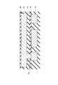
図10は本発明の第三実施形態における半導体装置を示し、図10[1]は半導体装置の回路図であり、図10[2]は半導体装置に含まれる容量素子の平面図である。以下、この図面に基づき説明する。
図10[1]の半導体装置100は、逐次比較型AD(Analog to Digital)変換回路であり、コンパレータ101、容量アレイ102、スイッチ部103等を備えている。本回路を用いてアナログ値をデジタル値へ変換するためには、容量値Cを有する容量素子を単位として、1倍、2倍、4倍、8倍・・・と、2の倍数で増加させた各容量素子が必要となる。Nビットのデジタル値に変換する場合、最大で2N-1Cの容量が必要となり、合計として2NCの容量が必要となる。本回路を構成するに当たっては、Cの容量を有する単位容量素子を2Nのアレイ状に並べる容量アレイ102を用いるのが一般的である。例えば、10ビットのAD変換回路を実現するためには210=1024個、12ビットのAD変換回路を実現するためには212=4096個の容量素子を並べる必要がある。なお、逐次比較型AD変換回路自体は周知であるので、その動作の詳しい説明は省略する。
図10[2]に、容量アレイ102の平面構成図を示す。容量アレイ102の各容量素子30は、図1に示す容量素子30と同様の構成である。一個の容量素子30は、第二のCu配線層と同時に形成される第一の下部電極32、第一の下部電極32を内部に含む形状で開口部44を有する容量素子層間膜、及び積層体65で構成されている。図10[2]では、積層体65よりも上にある層を除去して示している。
積層体65は、5nm~30nmの膜厚のTaNからなる第二の下部電極、5nm~15nmの膜厚のSiNからなる容量絶縁膜、20nm~100nmの膜厚のTiNからなる上部電極、及びエッチング停止層から構成される。本実施形態の場合、極めて多数の容量素子30を並べる必要があるため、単位面積当たりの容量を高くし、容量面積を小さくすることが重要である。この目的のため、容量絶縁膜としてSiNよりも誘電率の高いTaOを用いることが効果的である。容量絶縁膜として用いるTaOは、金属Taをスパッタ法によって3nm~7nm成膜し、350℃の酸化プラズマ雰囲気で酸化処理することによって形成する。このほか、スパッタ雰囲気に酸素を導入した反応性スパッタによって成膜してもよいし、CVD法などの気相成長法を用いることも可能である。
半導体装置100によれば、低寄生抵抗かつ高信頼性を有する容量素子30を用いていることから、信頼性を向上できる。
図11及び図12は本発明の第四実施形態における半導体装置を示し、図11[1]はシグナルフロー図であり、図11[2]は半導体装置中の変換部の構成図であり、図12[1]は変換部中の演算増幅回路の回路図であり、図12[2]は演算増幅回路中の容量素子の平面図である。以下、これらの図面に基づき説明する。
図11[1]に示す半導体装置200は、パイプライン型AD変換回路であり、ビットごとの複数の変換部201、各変換部201から出力された1ビットの信号から所定のコードのデジタル信号を出力するコード変換回路202等を備えている。半導体装置200では、入力されたアナログ値が、各段で最上位ビットから1ビット分ずつデジタル信号として出力される。Nビットの変換には、N-1段の変換部201が必要になる。各段では、一つの信号の処理を終えると、次の周期では次の信号の処理を行うことが可能である。そのため、半導体装置200は、全ビットの出力を待たずして、次の信号処理を開始するという特徴を有する。なお、パイプライン型AD変換回路自体は周知であるため、その動作の詳しい説明は省略する。
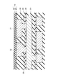
図11[2]は、各段の変換部201の構成を示す。変換部201は、演算増幅回路210、サンプルホールド回路221、ADC(Analog-Digital Converter)222、DAC(Digital-Analog Converter)223等を備えている。演算増幅回路210については、詳しい構成を図12[1]に示す。
図12[1]の演算増幅回路210は、オペアンプ211、キャパシタ回路212等からなるスイッチトキャパシタを用いている。この構成では、キャパシタC1,C2の相対精度が極めて重要な要素となる。相対精度は、容量素子のサイズに依存しており、サイズが大きいほど精度が向上する。
図12[2]に、演算増幅回路210に適用する容量素子のレイアウトを示す。キャパシタC1,C2は、図示するように、図1の容量素子30と同等の構成である。キャパシタC1,C2は相互に隣接している。一個の容量素子30は比較的大きな面積となるため、第一の下部電極32の面積が大きくなる。しかしながら、Cu配線はその製造上の問題から、連続した大面積パターンとすることは難しい。通常、Cu配線は、溝部に埋設したCuの余剰部分をCMP(Chemical Mechanical Polishing)による研磨で除去することで形成する。このとき、大面積のCuを用いると、中央部で研磨速度が上昇し、凹んだ形状となる。このことを抑制するため、第一の下部電極32を図示するように格子状に形成することが有効である。この場合でも、第一の下部電極32の全ての部分が、開口部44の内部にのみ存在するようにレイアウトする。積層体65は、開口部44を内包する形状で形成する。なお、図12[2]では、積層体65よりも上にある層を除去して示している。
半導体装置200によれば、低寄生抵抗かつ高信頼性を有する容量素子30を用いていることから、信頼性を向上できる。
図13は本発明の第五実施形態における半導体装置を示す平面図である。以下、この図面に基づき説明する。
本実施形態の半導体装置300は、AD変換回路301、無線入力回路302、PLL回路303、有線入出力回路304、デジタル回路305、記憶回路306を一チップ上に搭載している。AD変換回路301には容量素子30a、無線入力回路302には容量素子30b、PLL回路303には容量素子30c、デジタル回路305には容量素子30dがそれぞれ含まれている。容量素子30a~30dは、図1の容量素子30と同等の構成である。
AD変換回路301は第三実施形態又は第四実施形態で述べたものであり、これと同様にDA変換回路も搭載することも可能である。無線入力回路302は、外部からの無線信号を通すためのパスコンデンサとして容量素子30bを活用する。このとき、高周波応答性が重要であるため、容量素子30bの低寄生抵抗という特徴が極めて有効である。また、無線入力回路302でのアナログ信号処理においては、特定の周波数のみ通したりする回路も搭載され、その回路でも容量素子30bは用いられる。PLL回路303は、特定の周波数を発生させるためのであり、周波数のずれをフィードバックさせる際のループフィルタとして容量素子30cを用いる。デジタル回路305でも、同時に多数の素子がスイッチングする際に発生する同時スイッチングノイズを低減させるために、容量素子30dが有効に働く。このように、容量素子はさまざまな回路で活用されるが、本発明による容量素子30a~30dは、全ての用途に用いることが可能であり、複数の機能を搭載した半導体装置300において極めて有効な素子となる。
以上、上記各実施形態を参照して本発明を説明したが、本発明は上記各実施形態に限定されるものではない。本発明の構成や詳細については、当業者が理解し得るさまざまな変更を加えることができる。また、本発明には、上記各実施形態の構成の一部又は全部を相互に適宜組み合わせたものも含まれる。
この出願は2008年1月18日に出願された日本出願特願2008-009654を基礎とする優先権を主張し、その開示の全てをここに取り込む。
本発明は、例えばLSI(Large Scale Integrated circuit)中に組み込む容量素子、詳しくは多層配線を有するLSI中において導電性の上部電極膜-容量絶縁膜-導電性の下部電極から構成される容量素子に利用される。
10、100、200、300 半導体装置
11 CMOSトランジスタ層
12 Cu多層配線層
13 Cu配線層
14 配線キャップ絶縁膜
15 ビア層間膜
16 ビアプラグ
23 第一のCu配線層
24 第一のビアプラグ
25 ビアプラグ
26 配線キャップ絶縁膜
30、30a、30b、30c、30d 容量素子
31 第二のCu配線層
32 第一の下部電極
33 ビア層間膜
40 容量素子層間膜(層間絶縁膜)
41 配線キャップ絶縁膜
42 ハードマスク絶縁膜
43 ハードマスク絶縁膜の開口部
44 容量素子層間膜の開口部
51 エッチング停止層
61 第二の下部電極
62 容量絶縁膜
63 上部電極
71 第二のビアプラグ
72 コンタクトプラグ
75、76 第三のCu配線層
101 コンパレータ
102 容量アレイ
210 演算増幅回路
211 オペアンプ
301 AD変換回路
302 無線入力回路
303 PLL回路
304 有線入出力回路
305 デジタル回路
306 記憶回路
Claims (10)
- Cu配線層からなる第一の下部電極と、この第一の下部電極上に設けられるとともに当該第一の下部電極を内包する大きさの開口部を有する層間絶縁膜と、前記開口部を内包するように前記第一の下部電極上及び前記層間絶縁膜上に第二の下部電極、容量絶縁膜及び上部電極の順に設けられた積層体と、
を備えたことを特徴とする容量素子。 - 第一のCu配線層と、この第一のCu配線層にビアプラグを介して上方で接続された第二のCu配線層と、請求項1記載の容量素子とを備え、
前記第一の下部電極は、前記第一のCu配線層にビアプラグを介して接続されるとともに前記第二のCu配線層と同一層で形成されたCu配線層である、
ことを特徴とする半導体装置。 - 前記第二のCu配線層にビアプラグを介して上方で接続された第三のCu配線層を備え、
前記上部電極は、前記ビアプラグと同一層で形成されたコンタクトプラグを介して前記第三のCu配線層に接続された、
ことを特徴とする請求項2記載の半導体装置。 - 前記第二の下部電極と前記上部電極とは平面形状が同一である、
ことを特徴とする請求項2又は3のいずれか一項に記載の半導体装置。 - 前記層間絶縁膜は、Cu配線層の酸化及びCu元素の拡散を防止する性質を備えた配線キャップ絶縁膜と、この配線キャップ絶縁膜上に設けられ当該配線キャップ絶縁膜と異なる材質からなるハードマスク絶縁膜との二層を有する、
ことを特徴とする請求項2乃至4のいずれか一項に記載の半導体装置。 - 前記配線キャップ絶縁膜はSiCN又はSiCからなり、前記ハードマスク絶縁膜はSiO2又はSiCOHからなる、
ことを特徴とする請求項5記載の半導体装置。 - 前記開口部は上側が大きく開くテーパ形状である、
ことを特徴とする請求項2乃至6のいずれか一項に記載の半導体装置。 - 前記容量絶縁膜は膜厚5nm以上のSiNからなる、
ことを特徴とする請求項2乃至7のいずれか一項に記載の半導体装置。 - 前記容量絶縁膜はプラズマ酸化法によって形成されたタンタル酸化物からなる、
ことを特徴とする請求項2乃至7のいずれか一項に記載の半導体装置。 - Cu配線層からなる第一の下部電極と、この第一の下部電極上に設けられるとともに当該第一の下部電極を内包する大きさの開口部を有する層間絶縁膜と、前記開口部を内包するように前記第一の下部電極上及び前記層間絶縁膜上に第二の下部電極、容量絶縁膜及び上部電極の順に設けられた積層体とを備えた容量素子を製造する方法において、
前記第一の下部電極上を内包する面に前記層間絶縁膜を成膜する工程と、
前記層間絶縁膜をエッチングすることにより前記開口部を形成する工程と、
前記層間絶縁膜上及び前記開口部内の前記第一の下部電極上に、前記第二の下部電極となる第一層、前記容量絶縁膜となる第二層及び前記上部電極となる第三層を順次成膜する工程と、
前記第一層、前記第二層及び前記第三層を一括してエッチングすることにより、前記積層体を形成する工程と、
を含むことを特徴とする容量素子の製造方法。
Priority Applications (1)
| Application Number | Priority Date | Filing Date | Title |
|---|---|---|---|
| JP2009549996A JPWO2009090893A1 (ja) | 2008-01-18 | 2009-01-06 | 容量素子及びこれを備えた半導体装置並びに容量素子の製造方法 |
Applications Claiming Priority (2)
| Application Number | Priority Date | Filing Date | Title |
|---|---|---|---|
| JP2008-009654 | 2008-01-18 | ||
| JP2008009654 | 2008-01-18 |
Publications (1)
| Publication Number | Publication Date |
|---|---|
| WO2009090893A1 true WO2009090893A1 (ja) | 2009-07-23 |
Family
ID=40885284
Family Applications (1)
| Application Number | Title | Priority Date | Filing Date |
|---|---|---|---|
| PCT/JP2009/050023 WO2009090893A1 (ja) | 2008-01-18 | 2009-01-06 | 容量素子及びこれを備えた半導体装置並びに容量素子の製造方法 |
Country Status (2)
| Country | Link |
|---|---|
| JP (1) | JPWO2009090893A1 (ja) |
| WO (1) | WO2009090893A1 (ja) |
Cited By (1)
| Publication number | Priority date | Publication date | Assignee | Title |
|---|---|---|---|---|
| JP2011109074A (ja) * | 2009-10-22 | 2011-06-02 | Seiko Epson Corp | 集積回路装置及び電子機器 |
Citations (3)
| Publication number | Priority date | Publication date | Assignee | Title |
|---|---|---|---|---|
| JP2001237375A (ja) * | 1999-12-14 | 2001-08-31 | Toshiba Corp | Mimキャパシタ |
| JP2003264235A (ja) * | 2002-03-08 | 2003-09-19 | Fujitsu Ltd | 半導体装置及びその製造方法 |
| JP2004134451A (ja) * | 2002-10-08 | 2004-04-30 | Renesas Technology Corp | 半導体装置及びその製造方法 |
Family Cites Families (2)
| Publication number | Priority date | Publication date | Assignee | Title |
|---|---|---|---|---|
| JP3023298B2 (ja) * | 1995-10-25 | 2000-03-21 | 松下電子工業株式会社 | 半導体装置及びその製造方法 |
| JP3749776B2 (ja) * | 1997-02-28 | 2006-03-01 | 株式会社東芝 | 半導体装置 |
-
2009
- 2009-01-06 JP JP2009549996A patent/JPWO2009090893A1/ja active Pending
- 2009-01-06 WO PCT/JP2009/050023 patent/WO2009090893A1/ja active Application Filing
Patent Citations (3)
| Publication number | Priority date | Publication date | Assignee | Title |
|---|---|---|---|---|
| JP2001237375A (ja) * | 1999-12-14 | 2001-08-31 | Toshiba Corp | Mimキャパシタ |
| JP2003264235A (ja) * | 2002-03-08 | 2003-09-19 | Fujitsu Ltd | 半導体装置及びその製造方法 |
| JP2004134451A (ja) * | 2002-10-08 | 2004-04-30 | Renesas Technology Corp | 半導体装置及びその製造方法 |
Cited By (1)
| Publication number | Priority date | Publication date | Assignee | Title |
|---|---|---|---|---|
| JP2011109074A (ja) * | 2009-10-22 | 2011-06-02 | Seiko Epson Corp | 集積回路装置及び電子機器 |
Also Published As
| Publication number | Publication date |
|---|---|
| JPWO2009090893A1 (ja) | 2011-05-26 |
Similar Documents
| Publication | Publication Date | Title |
|---|---|---|
| JP5059784B2 (ja) | 半導体装置 | |
| US10373905B2 (en) | Integrating metal-insulator-metal capacitors with air gap process flow | |
| US8227893B2 (en) | Semiconductor device with capacitor element | |
| KR20010020476A (ko) | 자유 공간 유전체를 이용한 초고속 칩 상호 접속 | |
| JP2006352124A (ja) | 半導体デバイスおよびその構造体の製造方法 | |
| CN103456601A (zh) | 用于中介片的电容器及其制造方法 | |
| JP5601974B2 (ja) | 半導体装置及びその製造方法 | |
| JP2006216746A (ja) | 半導体装置 | |
| US9373679B2 (en) | Semiconductor device comprising capacitive element | |
| JP2011114049A (ja) | 半導体装置 | |
| JP5432662B2 (ja) | 電源配線構造の設計方法、半導体装置の製造方法、および、半導体装置 | |
| US20070077700A1 (en) | Capacitance process using passivation film scheme | |
| JP2005203672A (ja) | 半導体装置の製造方法 | |
| US20100006976A1 (en) | Semiconductor device and manufacturing method thereof | |
| WO2009090893A1 (ja) | 容量素子及びこれを備えた半導体装置並びに容量素子の製造方法 | |
| US7060193B2 (en) | Method to form both high and low-k materials over the same dielectric region, and their application in mixed mode circuits | |
| US20220367605A1 (en) | Method of forming a stress reduction structure for metal-insulator-metal capacitors | |
| US9136319B2 (en) | Method of making capacitor with a sealing liner and semiconductor device comprising same | |
| US11532695B2 (en) | Stress reduction structure for metal-insulator-metal capacitors | |
| US20230146512A1 (en) | Interconnects formed using integrated damascene and subtractive etch processing | |
| US7473984B2 (en) | Method for fabricating a metal-insulator-metal capacitor | |
| US20120211866A1 (en) | Metal-insulator-metal capacitor and a method of fabricating the same | |
| TW201042753A (en) | Integrated inductor | |
| KR20060110788A (ko) | 반도체 장치의 제조 방법 | |
| JP2004072107A (ja) | 変形されたデュアルダマシン工程を利用した半導体素子の金属配線形成方法 |
Legal Events
| Date | Code | Title | Description |
|---|---|---|---|
| 121 | Ep: the epo has been informed by wipo that ep was designated in this application |
Ref document number: 09701491 Country of ref document: EP Kind code of ref document: A1 |
|
| WWE | Wipo information: entry into national phase |
Ref document number: 2009549996 Country of ref document: JP |
|
| NENP | Non-entry into the national phase |
Ref country code: DE |
|
| 122 | Ep: pct application non-entry in european phase |
Ref document number: 09701491 Country of ref document: EP Kind code of ref document: A1 |