WO2008018392A1 - Method for manufacturing electronic circuit component - Google Patents
Method for manufacturing electronic circuit component Download PDFInfo
- Publication number
- WO2008018392A1 WO2008018392A1 PCT/JP2007/065296 JP2007065296W WO2008018392A1 WO 2008018392 A1 WO2008018392 A1 WO 2008018392A1 JP 2007065296 W JP2007065296 W JP 2007065296W WO 2008018392 A1 WO2008018392 A1 WO 2008018392A1
- Authority
- WO
- WIPO (PCT)
- Prior art keywords
- insulating layer
- layer
- temperature
- conductive layer
- electronic circuit
- Prior art date
Links
Classifications
-
- H—ELECTRICITY
- H10—SEMICONDUCTOR DEVICES; ELECTRIC SOLID-STATE DEVICES NOT OTHERWISE PROVIDED FOR
- H10K—ORGANIC ELECTRIC SOLID-STATE DEVICES
- H10K71/00—Manufacture or treatment specially adapted for the organic devices covered by this subclass
- H10K71/60—Forming conductive regions or layers, e.g. electrodes
- H10K71/611—Forming conductive regions or layers, e.g. electrodes using printing deposition, e.g. ink jet printing
-
- H—ELECTRICITY
- H10—SEMICONDUCTOR DEVICES; ELECTRIC SOLID-STATE DEVICES NOT OTHERWISE PROVIDED FOR
- H10K—ORGANIC ELECTRIC SOLID-STATE DEVICES
- H10K10/00—Organic devices specially adapted for rectifying, amplifying, oscillating or switching; Organic capacitors or resistors having a potential-jump barrier or a surface barrier
- H10K10/40—Organic transistors
- H10K10/46—Field-effect transistors, e.g. organic thin-film transistors [OTFT]
- H10K10/462—Insulated gate field-effect transistors [IGFETs]
- H10K10/466—Lateral bottom-gate IGFETs comprising only a single gate
-
- H—ELECTRICITY
- H10—SEMICONDUCTOR DEVICES; ELECTRIC SOLID-STATE DEVICES NOT OTHERWISE PROVIDED FOR
- H10K—ORGANIC ELECTRIC SOLID-STATE DEVICES
- H10K10/00—Organic devices specially adapted for rectifying, amplifying, oscillating or switching; Organic capacitors or resistors having a potential-jump barrier or a surface barrier
- H10K10/40—Organic transistors
- H10K10/46—Field-effect transistors, e.g. organic thin-film transistors [OTFT]
- H10K10/462—Insulated gate field-effect transistors [IGFETs]
- H10K10/468—Insulated gate field-effect transistors [IGFETs] characterised by the gate dielectrics
- H10K10/471—Insulated gate field-effect transistors [IGFETs] characterised by the gate dielectrics the gate dielectric comprising only organic materials
-
- H—ELECTRICITY
- H10—SEMICONDUCTOR DEVICES; ELECTRIC SOLID-STATE DEVICES NOT OTHERWISE PROVIDED FOR
- H10K—ORGANIC ELECTRIC SOLID-STATE DEVICES
- H10K10/00—Organic devices specially adapted for rectifying, amplifying, oscillating or switching; Organic capacitors or resistors having a potential-jump barrier or a surface barrier
- H10K10/80—Constructional details
- H10K10/82—Electrodes
- H10K10/84—Ohmic electrodes, e.g. source or drain electrodes
Definitions
- the present invention manufactures an electronic circuit component such as an organic electronic device or a wiring board in which a conductive layer functioning as an electrode, a conductor circuit, or the like is formed on an insulating layer by a low-temperature process of 200 ° C or lower. Therefore, the present invention relates to a novel electronic circuit component manufacturing method.
- an organic TFT 1 in this example includes a gate electrode 3 formed on a substrate 2 such as a flexible substrate, an insulating layer 4 covering the gate electrode 3, and spaced apart from each other on the insulating layer 4. And the semiconductor layer 7 filling the region between the source electrode 5 and the drain electrode 6 of the insulating layer 4.
- the gate electrode 3, the source electrode 5, and the drain electrode 6 are usually prepared by applying a dispersion liquid (such as a conductive paste) containing fine metal particles on the substrate 2 and the insulating layer 4. It is formed by printing, drying, and baking. Further, the insulating layer 4 is formed by using a dispersion liquid containing inorganic fine particles such as silicon oxide (SiO 2), aluminum oxide (Al 2 O 3), tantalum oxide (Ta 2 O 3), or a precursor thereof as a substrate 2 on which the gate electrode 3 is formed. It is formed by applying it on top, drying it, and firing it.
- a dispersion liquid such as a conductive paste
- the semiconductor layer 7 is usually formed by applying a coating liquid containing any organic semiconductor material to the source electrode
- the organic semiconductor material for forming the semiconductor layer 7 for example, various low molecular compounds and high molecular compounds having a ⁇ electron conjugated system in the molecule can be used.
- organic semiconductor materials include, for example, pentacene and thiophene oligomer derivatives as low-molecular compounds, and ⁇ -conjugated polymer compounds having a hetero five-membered ring and polyphenylene vinylene as polymer compounds. And polyacetylene (Patent Documents 1 to 4, Non-Patent Document 1).
- Patent Document 1 Japanese Published Patent: Japanese Patent No. 3006718
- Patent Document 2 Japanese Published Patent: JP-A-8-191162
- Patent Document 3 Japanese Published Patent: JP-A 62-85467
- Patent Document 4 Japanese Published Patent: Special Table 2001- 505002
- Patent 1 electrical properties of polyacetylene / polysiloxane interface, F. t ⁇ bi sawa et al., J. Appl. Phys., Vol. 54, No. 6, June 1983
- the conventional organic TFT is notably PC
- the firing temperature is limited by the heat-resistant temperature of the plastic substrate. That is, it cannot be improved sufficiently.
- the insulating layer formed using the dispersion liquid containing the inorganic fine particles and the precursor thereof described above is certainly the practical lower limit of the process temperature of the low-temperature polysilicon TFT process. Although it can be formed even if it is baked at a temperature lower than 250 ° C, it forms an insulating layer that has sufficient insulation and excellent adhesion to the substrate. In addition, in view of forming a conductive layer having excellent conductivity and excellent adhesion to the insulating layer, it is desirable to fire at as high a temperature as possible even within the above range.
- the firing temperature is limited by the heat-resistant temperature of the plastic substrate.
- a layer cannot be formed.
- the insulating layer made of inorganic fine particles and the plastic substrate are completely different materials chemically or characteristically in terms of thermal expansion coefficient, etc., and the adhesion between them is inherently low. This is one of the causes of the inability to form an insulating layer with excellent characteristics.
- the firing temperature is preferably as high as possible even within a range of 250 ° C or lower.
- the firing temperature is limited by the heat-resistant temperature of the plastic substrate, so that the firing is insufficient and a conductive layer having excellent characteristics can not be formed. Cases arise.
- An object of the present invention is to provide an insulating material having superior characteristics by processing at a process temperature of 200 ° C or lower, which does not affect the plastic substrate, etc., particularly on a general-purpose plastic substrate.
- An electronic circuit component manufacturing method capable of manufacturing a highly reliable electronic circuit component having a practical quality because a layer and a conductive layer can be formed. There is to do.
- the inventor firstly differs from the insulating layer made of inorganic fine particles in that the insulating layer is chemically or organically similar to the plastic substrate in terms of characteristics such as a thermal expansion coefficient. Therefore, it was examined to form an insulating layer with excellent adhesion on the plastic substrate using a resin that can form an insulating layer.
- a varnish obtained by dissolving at least one of polyimide and its precursor in an arbitrary solvent was applied on a plastic substrate, and then a temperature of 200 ° C. or lower. Insulating layer with excellent insulation, adhesion to plastic substrate, heat resistance, mechanical strength, etc. without affecting the general-purpose plastic substrate etc. It was found that it is preferable.
- the inventor next studied to reduce the firing temperature of the conductive layer such as an electrode formed on the insulating layer as much as possible.
- the melting temperature of the metal nanoparticles is reduced to the original, metal, by the so-called Kubo effect. Since the temperature can be lowered below the melting point, the temperature at which a large number of particles can be sintered well and a uniform conductive layer can be formed can be lowered to 200 ° C or lower. It has been found that a conductive layer having higher conductivity than conventional can be formed by firing at a temperature of 200 ° C. or lower.
- the inventor has studied to improve the adhesion between the insulating layer made of polyimide and the conductive layer made of metal nanoparticles. As a result, it was found that the adhesiveness of the conductive layer to the insulating layer can be improved when the contact angle of the insulating layer, which is an indicator of water wettability, is 80 ° or more.
- the first invention is an insulation in which a layer containing at least one of polyimide and its precursor is heated to a temperature of 200 ° C or lower and a contact angle with water is 80 ° or higher. Forming a coating layer made of a dispersion containing metal nanoparticles on the insulating layer, and baking the coating film at a temperature of 200 ° C. or lower to form a conductive layer.
- a method for manufacturing an electronic circuit component comprising: [0016] Further, the inventor also examined each component constituting the dispersion that is the basis of the conductive layer.
- the metal nanoparticles are composed of at least one metal selected from the group consisting of Ag, Au, Pt, Pd, Ru, Ir, Sn, Cu, Ni, Fe, Co, Ti, and In It has been found that the use of can further improve the conductivity of the conductive layer formed.
- the dispersion is a so-called aqueous dispersion containing metal nanoparticles, a dispersant that functions to uniformly disperse the metal nanoparticles in water, and water as a solvent
- the conductive layer is composed of Ag, Au, Pt, Pd, Ru, Ir, Sn, Cu, Ni, Fe, Co, Ti, and In whose primary particle diameter is lOOnm or less.
- a method for producing an electronic circuit component according to the first invention characterized in that the electronic circuit component is formed using a dispersion containing metal nanoparticles comprising at least one metal selected from the group, a dispersant, and water as a solvent. It is.
- an electronic circuit component includes a gate electrode formed on a substrate, an insulating layer covering the gate electrode, and a source electrode and a drain electrode formed on the insulating layer so as to be separated from each other. And a semiconductor layer that fills a region between the source electrode and the drain electrode of the insulating layer, and a layer including at least one of polyimide and a precursor thereof is formed on the substrate. After forming the insulating layer by covering the gate electrode and heating to a temperature of 200 ° C.
- a coating film made of a dispersion containing metal nanoparticles is patterned on the insulating layer.
- the conductive film is formed and the source electrode and the drain electrode are formed by firing the coating film at a temperature of 200 ° C. or lower. is there.
- the electronic circuit component manufacturing method of the present invention can also be suitably applied to manufacturing a wiring board such as a multilayer wiring board.
- the fourth invention is a wiring board in which an electronic circuit component has a conductor circuit formed on an insulating layer, and is a polyimide and its precursor. After forming an insulating layer by forming a layer including at least one of the above and heating to a temperature of 200 ° C. or less, a coating film having a dispersion force including metal nanoparticles is formed on the insulating layer.
- the electronic circuit component of the first or second invention is characterized in that a conductor circuit comprising a conductive layer is formed by forming a pattern and firing the coating film at a temperature of 200 ° C or lower. It is a manufacturing method.
- an insulation having superior characteristics can be obtained by processing at a process temperature of 200 ° C or lower, which does not affect the plastic substrate or the like, on a general-purpose plastic substrate or the like. Since it is possible to form a layer and a conductive layer, it is possible to manufacture a highly reliable electronic circuit component having a practical quality, and to provide a method for manufacturing an electronic circuit component. .
- FIG. 1 is a cross-sectional view showing a layer structure of an example of an organic TFT as an organic electronic device manufactured by the method for manufacturing an electronic circuit component of the present invention.
- a layer containing at least one of polyimide and a precursor thereof (hereinafter sometimes abbreviated as "polyimide compound”) is heated to a temperature of 200 ° C or lower.
- polyimide compound a precursor thereof
- an insulating layer having a contact angle with water of 80 ° or more and to form a coating film having a dispersion force containing metal nanoparticles on the insulating layer.
- a conductive layer by baking at a temperature of 200 ° C. or lower.
- Polyimide compounds that form the insulating layer include compounds represented by formulas (1) and (2):
- A represents a tetravalent organic group
- B represents a divalent organic group
- the above can be used.
- a polyamic acid that is a repeating unit represented by the formula (1) to a polyimide that is a repeating unit represented by the almost full force formula (2) of the repeating unit, from a polyamic acid that is a repeating unit represented by the formula (1).
- a single compound that can form an insulating layer with excellent insulating properties can be formed by forming a film at a temperature of 200 ° C. or less. Can be used in or in combination of two or more.
- the polyimide that forms the insulating layer after film formation does not impair the insulating properties, and as is well known, it contains unreacted polyamic acid or the unreacted polyamic acid moiety in the polyimide molecule. May be included. The same applies to the case where “insulating layer made of polyimide” is described below.
- the polyimide compound is not limited to this, but, for example, as in the prior art, a tetracarboxylic acid containing a group A or an anhydride thereof (such as a dianhydride) and a diamine compound containing a group B are subjected to a polymerization reaction. Can be synthesized.
- an insulating layer formed by heating to a temperature of 200 ° C or less and having a contact angle of 80 ° or more, which is an indicator of water wettability, is used.
- the contact angle of the insulating layer is set within the above range, the adhesion of the conductive layer to the insulating layer can be improved.
- the polyimide compound it is preferable to use a compound having a contact angle with water of 90 ′ 00 ° even within the above range.
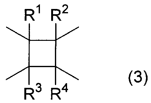
- a in the formulas (1) and (2) is represented by the formula (3):
- I ⁇ to R 4 are the same or different and each represents a hydrogen atom, a fluorine atom, or a monovalent organic group having 1 to 4 carbon atoms. ]
- xi x 3 is the same or different and represents an O— group, a CO—O— group, a CO—S— group, a —CO—NH group, a carbon number;! Or an alkylene group which may have a branched structure, a straight-chain alkylene group having a carbon number of! To 5 or an optionally branched alkylene dioxo group.
- ⁇ ⁇ x 3 can also be a single bond.
- R 5 represents an alkyl group having 6 or more carbon atoms or a fluorine-containing alkyl group having 6 or more carbon atoms.
- m and n are the same or different and represent 0 or 1.
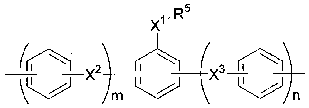
- a polyimide compound in which the remainder of B is a group having no X 1 ! ⁇ Group in the formula (4).
- the polyimide-based compound to adjust the ratio of groups among type B (4), the number of carbon atoms of the alkyl Le group for R 5, the Suto of fluorine atoms in the fluorinated alkyl group for R 5
- the contact angle which is an indicator of the wettability of the insulating layer with respect to water
- the proportion of the group of the formula (4) is 20 mol% or more, especially 50 mol% or more, especially 70 to 100 mol within the above range. / 0 is preferred.
- the carbon number of the alkyl group of R 5 or the fluorine-containing alkyl group is preferably 10 to 30, particularly 15 to 20 within the above range.
- suitable polyimide compound include, for example, at least one of the repeating units of the formulas (1) and (2), that is, the proportion of the repeating unit of the formula (1) is 0 to 100 mol. %, I ⁇ to R 4 in formula (3) are all hydrogen atoms, 100 mol% of B is a group of formula (4), and X 1 in formula (4) is an —O— group, R 5 And a polyimide compound in which m and n are 0, as well as an alkyl group having 18 carbon atoms.
- the polyimide compound is dissolved in an arbitrary organic solvent as in the prior art.
- Force to apply varnish to the surface by any coating method such as dip coating, spin coating, mouth coating, spray coating, bar coating, die coating, slit coating, brush coating, etc.
- the insulating layer when it is formed into a pattern, it may be dried after printing by an arbitrary printing method such as a transfer printing method, an ink jet printing method, or a screen printing method.
- a heating device such as a hot plate or an oven may be used to heat and dry in the air, in an inert gas such as nitrogen, or in the air.
- Heat drying may be performed in a temperature range in which the organic solvent is evaporated and the varnish can be dried.
- the temperature is preferably 40 ° C or higher and lower than 150 ° C.
- the layer is insulated by heating it in an arbitrary environment such as in the air, in an inert gas such as nitrogen, or in a vacuum using a heating device such as a hot plate or an oven.
- a heating device such as a hot plate or an oven.
- the heating temperature needs to be in a temperature range of 200 ° C. or less that does not affect a general-purpose plastic substrate or the like, and is preferably 150 to 180 ° C. in particular.
- the formation of the layer by drying the varnish and the formation of the insulating layer by heating the layer are performed by changing the heating temperature stepwise or continuously in the same atmosphere using the same heating device. However, it will continue to be fi.
- the thickness of the insulating layer formed through the above steps can be set in an arbitrary range according to the type of electronic circuit component to be manufactured.
- electronic circuit components In the case of an organic electronic device such as an organic TFT, and the insulating layer is an insulating layer covering the gate electrode (and its thickness power is 20 to 1000 nm, preferably 50 to 800 nm, especially 100 to 500 nm.
- the electronic circuit component is a wiring board such as a multilayer wiring board
- the insulating layer is an insulating layer that insulates between upper and lower conductor circuits laminated in the thickness direction. 1— 5. O ⁇ m, in particular 0.3-3. 0 to 111, in particular 0.5 to 1.5, preferably 1.5 to 1.
- O ⁇ m in particular 0.3-3. 0 to 111, in particular 0.5 to 1.5, preferably 1.5 to 1.
- a coating film made of a dispersion containing metal nanoparticles is formed on the insulating layer.
- the metal nanoparticles various particle forces S made of any metal and having a primary particle diameter of nanometer level can be used.
- the effect of forming a uniform conductive layer by satisfactorily sintering between a large number of particles by the Kubo effect described above is further improved, and the conductivity of the conductive layer formed thereby is improved.
- the metal nanoparticles include Ag, Au, Pt, Pd, whose primary particle size is less than lOOnm.
- the primary particle diameter of the metal nanoparticles is preferably 1 nm or more even in the above range for practical use. In the present invention, the primary particle diameter is expressed as 50% diameter (D) of the particle size distribution of the metal nanoparticles measured using a particle size distribution measuring apparatus applying the laser Doppler method.
- the conductive layer may be formed of any one of the above-mentioned various metals alone or in combination of two or more.
- metal nanoparticles made of an alloy of the two or more kinds of metals may be used as the metal nanoparticles, or individual metal simple substance or You may use together 2 or more types of metal nanoparticles which consist of an alloy of some metals among all the metals which form a conductive layer.
- the conductive layer is required to have particularly high conductivity, the conductive layer is formed of Ag having excellent conductivity, or an alloy containing Ag at a ratio of 50 atomic% or more. I like it!
- the metal nanoparticles for forming the conductive layer include Ag nanoparticles, Ag nanoparticles containing Ag in the above proportions, Ag nanoparticles or nanoparticles thereof, and other metals or alloys. And a mixture of metal nanoparticles such that the Ag ratio is in the above range. It is.
- the other metal that forms an alloy with Ag includes at least one metal selected from the group consisting of Au Pt Pd Ru Ir Sn Cu Ni Fe Co Ti, and In.
- the metal nanoparticles can be produced by various conventionally known methods such as a high temperature treatment method called an impregnation method, a liquid phase reduction method, and a gas phase method.
- a high temperature treatment method called an impregnation method
- a liquid phase reduction method for example, in water, a water-soluble metal compound that is a source of metal ions forming the metal nanoparticles, a dispersant, And a reducing agent may be added, and metal ions may be preferably reduced and reacted for a certain period of time with vigorous stirring.
- a reducing agent may be added, and metal ions may be preferably reduced and reacted for a certain period of time with vigorous stirring.
- two or more water-soluble metal compounds that form ions of at least two kinds of metals are used in combination. That's fine.
- Metal nanoparticles produced by the liquid phase reduction method are characterized by being spherical or granular in shape, sharp in particle size distribution, and having a small primary particle size.
- water-soluble metal compounds that are the source of metal ions include, in the case of Ag, silver nitrate (I) [AgNO], silver methanesulfonate [CH 2 SO Ag], and the like.
- Ag silver nitrate (I) [AgNO]
- Ag silver methanesulfonate
- CH 2 SO Ag silver methanesulfonate
- any of various reducing agent forces that can be precipitated as metal nanoparticles by reducing metal ions in a liquid phase reaction system can be used.
- the reducing agent include sodium borohydride, sodium hypophosphite, hydrazine, and transition metal ions (trivalent titanium ions, divalent cobalt ions, etc.).
- transition metal ions trivalent titanium ions, divalent cobalt ions, etc.
- it is effective to reduce the metal ion reduction and deposition rate.
- Examples of the reducing agent having a weak reducing power include alcohols such as methanol, ethanol, 2-propanol, and ascorbic acid, as well as ethylene glycol, dartathione, organic acids (taenoic acid, malic acid, tartaric acid). Etc.), reducing sugars (glucose, galactose, mannose, funolectose, sucrose, manoletose, raffinose, stachyose, etc.) and sugar alcohols (sorbitol, etc.), among others, reducing sugars and derivatives thereof The sugar alcohols are preferred.
- the dispersant is a solid at room temperature with a molecular weight of 000 to 30000, and has a good solubility in water, and the deposited metal nanoparticles are well dispersed in water.
- Various dispersants that can be used are preferably used.
- the dispersing agent exists in the reaction system so as to surround the periphery of the deposited metal nanoparticles, and functions to prevent aggregation of the metal nanoparticles and maintain dispersion.
- the liquid phase reaction system in which the metal nanoparticles are deposited is Without separating metal nanoparticles from the reaction system, it can be used as a starting material for preparing a dispersion liquid containing metal nanoparticles and forming a conductive layer in a state in which only impurities are removed. .
- the dispersant remains almost removed in the impurity removal step, and serves to prevent the metal nanoparticles from agglomerating and maintain dispersion in the dispersion as described above. Keep doing.
- the molecular weight of the dispersant is less than 2000, there is a possibility that the effect of maintaining the dispersion by preventing aggregation of metal nanoparticles by the dispersant may not be obtained. For this reason, a conductive layer formed by applying a dispersion containing metal nanoparticles to the surface of the insulating layer described above and then firing is formed so that the film quality is smooth and dense, and there are no voids. There are cases where it cannot be done.
- a dispersant having a molecular weight exceeding 30000 is too bulky, it inhibits the sintering of metal nanoparticles in the firing step when forming a conductive layer, and causes voids or the denseness of the film quality.
- the residue of the dispersing agent may remain as an impurity in the conductive layer, thereby reducing the conductivity of the conductive layer.
- a dispersant having a molecular weight of 2000 to 30000 is excellent in the function of favorably dispersing the metal nanoparticles in the dispersion liquid and is not too bulky. It does not cause voids or reduce the density of the film quality, and does not leave decomposition residues that cause a decrease in conductivity in the conductive layer.
- the dispersing agent is an electronic component disposed in the vicinity of the conductive layer when used in the field of electronics such as the organic electronic device such as the organic TFT described above or the wiring substrate such as a multilayer wiring substrate. In view of preventing the deterioration of the material, sulfur, phosphorus, boron, and hydrogen are preferred, and do not contain the rogen atom! /.
- Suitable dispersants that satisfy these conditions include, for example, amine polymer dispersants such as polyethyleneimine and polypyrrolidone, polyacrylic acid, and carboxymethylol cellulose.
- amine polymer dispersants such as polyethyleneimine and polypyrrolidone
- polyacrylic acid polyacrylic acid
- carboxymethylol cellulose a hydrocarbon-based polymer dispersant having a carboxylic acid group, poval (polybutyl alcohol), or a copolymer having a polyethyleneimine moiety and a polyethylene oxide moiety in one molecule, etc.
- polymeric dispersants having a polar group those having a molecular weight in the range of 2000-30000 can be mentioned.
- the dispersant can be water or Can also be added to the reaction system in the form of a solution dissolved in a water-soluble organic solvent.
- the types and blending ratios of the metal compound, the dispersant, and the reducing agent are adjusted, and when the metal compound is subjected to the reduction reaction,
- the degree, time, pH, etc. may be adjusted.
- the pH of the reaction system is preferably 7 to 13 in consideration of forming metal nanoparticles having a primary particle size as small as possible.
- a pH adjusting agent is used.
- alkali metal, Nitric acid and ammonia that do not contain alkaline earth metals, halogen elements such as chlorine, and impurity elements such as sulfur, phosphorus, and boron are preferable.
- the metal nanoparticles precipitated in the liquid phase reaction system are subjected to processes such as mashing, washing, drying, and crushing, and then once converted into a powder form, water, a dispersant, and further necessary.
- a water-soluble organic solvent may be blended at a predetermined ratio to prepare a dispersion liquid that will form the coating film containing the metal nanoparticles.
- the dispersion is preferably prepared using a liquid phase reaction system in which nanoparticles are deposited as a starting material. That is, from the liquid phase reaction system containing the metal nanoparticles after precipitation of the metal nanoparticles and the water used for the reaction, treatment such as ultrafiltration, centrifugation, washing with water, and electrodialysis is performed.
- the concentration of metal nanoparticles can be adjusted by concentrating and removing water as needed, or by adding water.
- a dispersion liquid containing metal nanoparticles is prepared by combining the organic solvent in a predetermined ratio. In this method, generation of coarse and irregular particles due to aggregation of metal nanoparticles can be prevented, and a more dense and uniform conductive layer can be formed.
- the water content in the dispersion is preferably 20 to 400 parts by weight per 100 parts by weight of the metal nanoparticles.
- the water-based dispersant is sufficiently swollen, and the metal nanoparticles surrounded by the dispersant are dispersed well in the dispersion without causing aggregation. There is a possibility that the effect to be obtained is not sufficiently obtained.
- the coating layer having a sufficient thickness and density, and the conductive layer are formed on the surface of the insulating layer described earlier when the content ratio of the metal nanoparticles in the dispersion is reduced. Can't form!
- water-soluble organic solvent various organic solvents that are water-soluble can be used. Specific examples thereof include methyl alcohol, ethyl alcohol, n -propyl alcohol, isopropyl alcohol, n-butyl alcohol, isobutyl alcohol, alcohols such as sec-butanol alcohol, tert-butyl alcohol, acetone, and methyl ethynole ketone. Examples thereof include polyalcohols such as ketones, ethylene glycol and glycerin, and estenoles thereof, and dallic ethers such as ethylene glycol-monomono chinenoate ether and diethylene glycol mono-monobutyl ether.
- the content of the water-soluble organic solvent is preferably 30 to 900 parts by weight per 100 parts by weight of the metal nanoparticles. If the content ratio of the water-soluble organic solvent is less than the above range, the effect of adjusting the viscosity and vapor pressure of the dispersion due to the inclusion of the organic solvent may not be sufficiently obtained. When the above range is exceeded, the dispersant is sufficiently swollen with water by an excess organic solvent, and the metal nanoparticles surrounded by the dispersant are aggregated in the dispersion. There is a possibility that the effect of dispersing well without letting
- the content of the dispersant is preferably 3 to 60 parts by weight per 100 parts by weight of the metal nanoparticles.
- the content ratio of the dispersant is less than the above range, the presence of the dispersant is present in the dispersion liquid containing water so as to surround the metal nanoparticles, thereby preventing the aggregation. There is a possibility that it cannot be obtained sufficiently.
- an excessive dispersant may inhibit the sintering of the metal nanoparticles, thereby generating voids or reducing the denseness of the film quality.
- Decomposition residue of polymer dispersant 1S It remains as an impurity in the conductive layer, which may decrease the conductivity of the conductive layer.
- Examples of the coating method for forming a coating film by applying the dispersion to the surface of the insulating layer include, for example, a dip coating method, a spin coating method, a roll coating method, a spray coating method, and a no coating method. , Die coating method, slit coating method, or brush coating method.
- a dip coating method a spin coating method
- a roll coating method a spray coating method
- a no coating method Die coating method, slit coating method, or brush coating method.
- the dispersion can be uniformly applied to the surface of the insulating layer, it is possible to make the thickness of the conductive layer formed through the subsequent baking process even more uniform. it can.
- Application In order to form a pattern of the coating film formed by the method into a predetermined planar shape, for example, etching using a photolithography method is preferably employed. Etching using the photolithographic method requires the ability to form fine patterns such as source and drain electrodes of organic electronic devices or conductor circuits of wiring boards with high accuracy
- a resist mask that covers a region corresponding to a pattern to be formed is formed by laminating a photosensitive resist layer on the dried coating film, exposing the resist layer, and developing the resist layer. After the film is formed, the coating film exposed without being covered with the resist mask is selectively etched and removed, whereby the coating film is patterned into a predetermined planar shape.
- a liquid phase method using an etching solution and a gas phase method using an etching gas or an ion beam. It may be adopted.
- the liquid phase method is preferable in consideration of preventing the deterioration of the substrate.
- a temperature at which the organic substances contained in the coating film can be thermally decomposed and the metal nanoparticles can be sintered. To heat.
- Firing may be performed in the air in order to thermally decompose the organic matter, and in order to prevent oxidation of the metal nanoparticles, after firing in the air, in a non-oxidizing atmosphere or a reducing atmosphere. Further firing may be performed in an atmosphere.
- the firing temperature suppresses the crystal grain size of the metal constituting the conductive layer formed by the firing from becoming too large, voids in the conductive layer, and deterioration of the plastic substrate. As described above, it is preferably 200 ° C. or lower, particularly 150 to 180 ° C.
- the conductive layer can be patterned by etching or the like using a photolithographic method.
- the dispersion was printed on the surface of the insulating layer by a predetermined printing method such as a transfer printing method, an ink jet printing method, or a screen printing method in advance, and then baked to form a pattern. You can also get a conductive layer
- FIG. 1 shows an organic electronic device manufactured by the method for manufacturing an electronic circuit component of the present invention. It is sectional drawing which shows the layer structure of an example of organic TFT as a cell.
- an organic TFT 1 in this example is formed by separating a gate electrode 3 formed on a substrate 2, an insulating layer 4 covering the gate electrode 3, and the insulating layer 4 from each other.
- a source electrode 5 and a drain electrode 6, and a semiconductor layer 7 filling the region of the insulating layer 4 between the source electrode 5 and the drain electrode 6 are provided.
- the insulating layer 4, the source electrode 5 and the drain electrode 6 thereon are manufactured by the manufacturing method of the present invention.
- the layer containing the polyimide-based compound described above is formed on the substrate 2 so as to cover the gate electrode 3 formed in advance, and is heated to a temperature of 200 ° C. or less to insulate.
- a layer 4 is formed, and a coating film made of a dispersion containing metal nanoparticles is formed on the insulating layer 4 and baked at a temperature of 200 ° C. or lower to form a source electrode made of a conductive layer. 5 and the drain electrode 6 are formed.
- the other parts that make up the organic TFT can be formed in the same way as before.
- the substrate 2 when the organic TFT in the figure is an electronic device that individually drives pixels of a flexible display such as electronic paper, a flexible substrate such as a plastic substrate is used.
- a flexible substrate such as a plastic substrate is used.
- the insulating layer as described above, the insulating layer
- the source electrode 5 and the drain electrode 6 can be formed by a low-temperature process of 200 ° C or less, a low-cost, low-cost, general-purpose plastic substrate such as PC or PET should be used as the plastic substrate. Can do. Therefore, it is possible to promote the practical use of the flexible display such as the electronic paper by reducing the cost.
- the gate electrode 3 may be formed by a vacuum deposition method, a sputtering method, or the like, or, like the source electrode 5 and the drain electrode 6, formed by baking a coating film made of a dispersion containing metal nanoparticles. You may do it.
- the organic TFT can be formed only by a coating or printing process without requiring a process using a vacuum apparatus, so that the cost of a flexible display can be further reduced. it can.
- the baking temperature when baking the coating film is preferably 200 ° C. or lower in consideration of preventing the deterioration of the general-purpose plastic substrate.
- the semiconductor layer 7 is applied by applying the coating liquid containing the organic semiconductor material described above on the insulating layer 4 on which the source electrode 5 and the drain electrode 6 are formed so as to fill between the two electrodes, and then drying. Then, it can be formed by firing as necessary.
- the method for producing an electronic circuit component of the present invention is suitably employed as a method for producing an organic electronic device or a wiring board.
- organic electronic devices that can be manufactured by the manufacturing method of the present invention include organic TFTs, organic field effect transistors (FETs), organic electroluminescent (EL) elements, organic light energy conversion elements, sensor elements, etc. .
- a wiring board a single layer or a multilayer wiring board etc. are mentioned. Example
- a polymerization reaction with the diamine compound represented by the formula (1) consisting only of the repeating unit of the formula (1) explained above, wherein A in the formula (1) is a group of the formula (3) and (3) I ⁇ to R 4 are all hydrogen atoms in at 100 mol% groups of the formula (4) in B, and, X 1 in the formula (4) is - O-group, R 5 carbon atoms
- a polyimide compound having 18 alkyl groups and m and n of 0 was synthesized.
- N-methyl-2 as an organic solvent was synthesized with the polyimide compound synthesized previously.
- a varnish dissolved in pyrrolidone and having a polyimide compound concentration of 6% by weight is dropped using a syringe with a filter having a pore size of 0.2 mm, and a layer is formed on the ITO film by spin coating. After being formed, in the atmosphere, using a hot plate heated to 80 ° C, heat to dry for 5 minutes, then raise the pot plate temperature to 200 ° C and heat for 60 minutes. Thus, an insulating layer was formed.
- the thickness of the insulating layer was about 200 nm.
- the contact angle of the insulating layer with pure water was measured at a temperature of 25 ⁇ 2 ° C and a relative humidity of 50 ⁇ 5% in a constant temperature-humidity environment (Kaiwa Interface Science Co., Ltd. W] was measured at a liquid volume of 31 and after standing for 5 seconds, it was 96 °.
- Ag nanoparticles having a primary particle diameter of 20 nm, a mixed solvent of water and propylene glycol monomethyl ether as a solvent, and a carboxylic acid polymer dispersion An Ag nanoparticle dispersion containing an agent (molecular weight 15000) is dropped using a syringe with a filter having a pore size of 0.2 ⁇ m, and a coating film is formed on the insulating layer by a spin coating method. After drying, a conductive layer having a thickness of about 200 nm was formed by firing using a hot plate under any of the following conditions.
- Condition 1 150 ° C, 120 minutes
- Equation (7)
- An insulating layer was formed in the same manner as in Example 1 except that a polyimide compound synthesized by polymerization reaction with a diamine compound represented by the following formula was used, and the contact angle with pure water was It was 70 ° when measured under the same conditions as in Example 1. Next, a conductive layer having a thickness of about 200 nm was formed on the insulating layer in the same manner as in Example 1.
- hexamethyldisilazane 03 manufactured by Aldrich
- the insulating layer was formed by spin coating.
- a coating film is formed on the substrate, dried at 100 ° C. for 5 minutes using a hot plate, and then allowed to stand at room temperature, and then rinsed with acetone to hydrophobize the insulating layer, and then add pure water.
- the contact angle measured under the same conditions as in Example 1 was 90 °.
- a conductive layer having a thickness of about 200 nm was formed on the insulating layer in the same manner as in Example 1.
- Comparative Example 1 in which a conductive layer is formed on an insulating layer made of a polyimide-based compound but having a contact angle with pure water of 80 ° or less has a condition for firing the conductive layer.
- the adhesion of the conductive layer was good only under the condition 1 (150 ° C., 120 minutes), but it was found that the adhesion of the conductive layer was poor under other conditions.
- Comparative Examples 2 and 3 in which the insulating layer is an inorganic insulating layer having SiO force, the adhesiveness of the conductive layer is poor under any conditions related to the contact angle of the insulating layer with pure water.
- Example 1 in which a conductive layer was formed on an insulating layer made of a polyimide-based compound and having a contact angle with pure water of 80 ° or more, the conditions for firing the conductive layer were the above conditions;! In any case of ⁇ 3, it was confirmed that the adhesion of the conductive layer was good.
- Ag nanoparticle dispersion that is the source of the conductive layer
- a conductive layer was formed on the surface of the insulating layer in the same manner as in Example 1 and Comparative Examples 1 to 3 except that an agent containing an agent (molecular weight 15000) was used, and adhesion was evaluated. The results are shown in Table 2.
- Comparative Example 4 in which a conductive layer is formed on an insulating layer that is made of a polyimide compound but has a contact angle with pure water of 80 ° or less is based on condition 1 (150 ° C 120 minutes), the adhesion of the conductive layer was good, but it was found that the adhesion of the conductive layer was poor under other conditions. Further, in Comparative Examples 5 and 6 in which the insulating layer is an insulative insulating layer made of SiO, the adhesiveness of the conductive layer is maintained under any conditions regardless of the contact angle of the insulating layer with pure water. Turned out to be bad.
- Example 2 in which a conductive layer was formed on an insulating layer made of a polyimide-based compound and having a contact angle with pure water of 80 ° or more, the conditions for firing the conductive layer were the above conditions; In any case of! To 3, it was confirmed that the adhesion of the conductive layer was good.
- the resistivity of the conductive layer was determined using a resistivity meter (Loresta GP MCP-T610, manufactured by Dia Instruments). It was measured. The results are shown in Table 3.
Abstract
Description


Claims
Priority Applications (3)
| Application Number | Priority Date | Filing Date | Title |
|---|---|---|---|
| CN2007800295504A CN101501821B (en) | 2006-08-07 | 2007-08-03 | Method for manufacturing electronic circuit component |
| US12/376,334 US8026185B2 (en) | 2006-08-07 | 2007-08-03 | Method for manufacturing electronic circuit component |
| EP07791969A EP2053639A4 (en) | 2006-08-07 | 2007-08-03 | Method for manufacturing electronic circuit component |
Applications Claiming Priority (2)
| Application Number | Priority Date | Filing Date | Title |
|---|---|---|---|
| JP2006214809A JP2008041960A (en) | 2006-08-07 | 2006-08-07 | Manufacturing method of electronic circuit component |
| JP2006-214809 | 2006-08-07 |
Publications (1)
| Publication Number | Publication Date |
|---|---|
| WO2008018392A1 true WO2008018392A1 (en) | 2008-02-14 |
Family
ID=39032923
Family Applications (1)
| Application Number | Title | Priority Date | Filing Date |
|---|---|---|---|
| PCT/JP2007/065296 WO2008018392A1 (en) | 2006-08-07 | 2007-08-03 | Method for manufacturing electronic circuit component |
Country Status (7)
| Country | Link |
|---|---|
| US (1) | US8026185B2 (en) |
| EP (1) | EP2053639A4 (en) |
| JP (1) | JP2008041960A (en) |
| KR (1) | KR20090040303A (en) |
| CN (1) | CN101501821B (en) |
| TW (1) | TWI433365B (en) |
| WO (1) | WO2008018392A1 (en) |
Families Citing this family (15)
| Publication number | Priority date | Publication date | Assignee | Title |
|---|---|---|---|---|
| JP2008311585A (en) * | 2007-06-18 | 2008-12-25 | Elpida Memory Inc | Wiring structure, semiconductor device, and their manufacturing methods |
| TWI401205B (en) * | 2008-01-31 | 2013-07-11 | Ind Tech Res Inst | Fabricating method for an applied substrate employing photo-thermal effect |
| JP5239700B2 (en) * | 2008-09-30 | 2013-07-17 | 住友金属鉱山株式会社 | Coating film forming method using metal fine particle dispersion and coating film using the same |
| JP5381244B2 (en) * | 2009-03-31 | 2014-01-08 | 大日本印刷株式会社 | Thin film transistor array manufacturing method and display device |
| JP2013511603A (en) * | 2009-11-20 | 2013-04-04 | イー・アイ・デュポン・ドウ・ヌムール・アンド・カンパニー | Interposer film useful in semiconductor packaging applications and methods related thereto |
| WO2011126076A1 (en) * | 2010-04-09 | 2011-10-13 | 大日本印刷株式会社 | Thin-film transistor substrate |
| EP2444522B1 (en) * | 2010-10-21 | 2017-04-05 | Rohm and Haas Electronic Materials LLC | Stable nanoparticles for electroless plating |
| WO2013011788A1 (en) * | 2011-07-15 | 2013-01-24 | シャープ株式会社 | Method for forming pattern and method for manufacturing electric wiring substrate |
| US9576872B2 (en) * | 2013-12-18 | 2017-02-21 | Infineon Technologies Ag | Semiconductor devices and methods for manufacturing semiconductor devices |
| JP6143698B2 (en) * | 2014-03-28 | 2017-06-07 | 富士フイルム株式会社 | Wiring pattern forming method, organic transistor manufacturing method, and organic transistor |
| CH710579A1 (en) * | 2014-12-23 | 2016-06-30 | Metalor Tech Int Sa | A method of electroless plating of a precious metal. |
| JP6473361B2 (en) * | 2015-03-25 | 2019-02-20 | スタンレー電気株式会社 | Electronic device manufacturing method and electronic device |
| JP6630053B2 (en) | 2015-03-25 | 2020-01-15 | スタンレー電気株式会社 | Electronic device manufacturing method |
| JP6491032B2 (en) | 2015-04-24 | 2019-03-27 | スタンレー電気株式会社 | Manufacturing method of resistor and resistor |
| EP3684146A4 (en) * | 2017-09-15 | 2021-06-02 | JSR Corporation | Circuit board |
Citations (10)
| Publication number | Priority date | Publication date | Assignee | Title |
|---|---|---|---|---|
| JPS6285467A (en) | 1985-10-09 | 1987-04-18 | Mitsubishi Electric Corp | Field effect transistor |
| JPH036718B2 (en) | 1984-04-02 | 1991-01-30 | Pioneer Electronic Corp | |
| JPH08191162A (en) | 1995-01-09 | 1996-07-23 | Matsushita Electric Ind Co Ltd | Field-effect transistor |
| JP2001505002A (en) | 1997-08-22 | 2001-04-10 | コーニンクレッカ フィリップス エレクトロニクス エヌ ヴィ | Method of fabricating a field effect transistor consisting essentially of organic material |
| JP2004296424A (en) * | 2003-03-11 | 2004-10-21 | Advanced Lcd Technologies Development Center Co Ltd | Method for forming metal layer, metal layer, and display device using metal layer |
| JP2005175472A (en) * | 2003-12-11 | 2005-06-30 | Xerox Corp | Method of depositing nanoparticles |
| JP2005223049A (en) * | 2004-02-04 | 2005-08-18 | Ricoh Co Ltd | Semiconductor device, its fabrication process, and display |
| JP2005353728A (en) * | 2004-06-09 | 2005-12-22 | Mitsubishi Electric Corp | High-frequency device |
| JP2006032916A (en) * | 2004-06-14 | 2006-02-02 | Semiconductor Energy Lab Co Ltd | Wiring board, semiconductor device, and its manufacturing method |
| JP2006214809A (en) | 2005-02-02 | 2006-08-17 | Canon Inc | Method of measuring euv mirror shape |
Family Cites Families (18)
| Publication number | Priority date | Publication date | Assignee | Title |
|---|---|---|---|---|
| JP3006718B2 (en) | 1990-09-25 | 2000-02-07 | 科学技術振興事業団 | Electronic devices using oligothiophene |
| US7217754B2 (en) * | 1997-02-26 | 2007-05-15 | Integument Technologies, Inc. | Polymer composites and methods for making and using same |
| JPH116718A (en) | 1997-06-17 | 1999-01-12 | Suzuka Fuji Xerox Kk | Solder defect inspecting instrument for printed circuit board |
| JP3565069B2 (en) | 1998-12-28 | 2004-09-15 | ソニーケミカル株式会社 | Method for manufacturing double-sided flexible printed circuit board |
| KR100839393B1 (en) * | 2001-07-26 | 2008-06-19 | 닛산 가가쿠 고교 가부시키 가이샤 | Polyamic acid resin composition |
| DE10153562A1 (en) * | 2001-10-30 | 2003-05-15 | Infineon Technologies Ag | Process for reducing the electrical contact resistance in organic field-effect transistors by embedding nanoparticles to produce field peaks at the interface between the contact material and the organic semiconductor material |
| GB0207134D0 (en) * | 2002-03-27 | 2002-05-08 | Cambridge Display Tech Ltd | Method of preparation of organic optoelectronic and electronic devices and devices thereby obtained |
| WO2005047967A1 (en) * | 2003-11-14 | 2005-05-26 | Semiconductor Energy Laboratory Co., Ltd. | Liquid crystal display device and method for manufacturing the same |
| US7494923B2 (en) | 2004-06-14 | 2009-02-24 | Semiconductor Energy Laboratory Co., Ltd. | Manufacturing method of wiring substrate and semiconductor device |
| CN1741298B (en) | 2004-08-23 | 2010-07-14 | 财团法人工业技术研究院 | Method for raising organic semiconductor carrier mobility |
| JP4502382B2 (en) * | 2004-11-02 | 2010-07-14 | キヤノン株式会社 | Organic transistor |
| EP1670079B1 (en) * | 2004-12-08 | 2010-12-01 | Samsung Mobile Display Co., Ltd. | Method of forming a conductive pattern of a thin film transistor |
| JP2006173532A (en) * | 2004-12-20 | 2006-06-29 | Nippon Hoso Kyokai <Nhk> | Organic transistor and forming method for organic transistor |
| JP4779974B2 (en) * | 2004-12-22 | 2011-09-28 | 日産化学工業株式会社 | Liquid crystal aligning agent and liquid crystal display element using the same |
| JP4162659B2 (en) | 2005-01-11 | 2008-10-08 | 株式会社有沢製作所 | Flexible printed wiring board, multilayer flexible printed wiring board, and mobile phone terminal using the multilayer flexible printed wiring board |
| TWI412138B (en) * | 2005-01-28 | 2013-10-11 | Semiconductor Energy Lab | Semiconductor device, electronic device, and method of manufacturing semiconductor device |
| US7306969B2 (en) * | 2005-07-22 | 2007-12-11 | Xerox Corporation | Methods to minimize contact resistance |
| US7718707B2 (en) * | 2006-12-21 | 2010-05-18 | Innovalight, Inc. | Method for preparing nanoparticle thin films |
-
2006
- 2006-08-07 JP JP2006214809A patent/JP2008041960A/en active Pending
-
2007
- 2007-08-03 WO PCT/JP2007/065296 patent/WO2008018392A1/en active Application Filing
- 2007-08-03 EP EP07791969A patent/EP2053639A4/en not_active Withdrawn
- 2007-08-03 CN CN2007800295504A patent/CN101501821B/en not_active Expired - Fee Related
- 2007-08-03 KR KR1020097001616A patent/KR20090040303A/en not_active Application Discontinuation
- 2007-08-03 US US12/376,334 patent/US8026185B2/en not_active Expired - Fee Related
- 2007-08-06 TW TW096128828A patent/TWI433365B/en not_active IP Right Cessation
Patent Citations (10)
| Publication number | Priority date | Publication date | Assignee | Title |
|---|---|---|---|---|
| JPH036718B2 (en) | 1984-04-02 | 1991-01-30 | Pioneer Electronic Corp | |
| JPS6285467A (en) | 1985-10-09 | 1987-04-18 | Mitsubishi Electric Corp | Field effect transistor |
| JPH08191162A (en) | 1995-01-09 | 1996-07-23 | Matsushita Electric Ind Co Ltd | Field-effect transistor |
| JP2001505002A (en) | 1997-08-22 | 2001-04-10 | コーニンクレッカ フィリップス エレクトロニクス エヌ ヴィ | Method of fabricating a field effect transistor consisting essentially of organic material |
| JP2004296424A (en) * | 2003-03-11 | 2004-10-21 | Advanced Lcd Technologies Development Center Co Ltd | Method for forming metal layer, metal layer, and display device using metal layer |
| JP2005175472A (en) * | 2003-12-11 | 2005-06-30 | Xerox Corp | Method of depositing nanoparticles |
| JP2005223049A (en) * | 2004-02-04 | 2005-08-18 | Ricoh Co Ltd | Semiconductor device, its fabrication process, and display |
| JP2005353728A (en) * | 2004-06-09 | 2005-12-22 | Mitsubishi Electric Corp | High-frequency device |
| JP2006032916A (en) * | 2004-06-14 | 2006-02-02 | Semiconductor Energy Lab Co Ltd | Wiring board, semiconductor device, and its manufacturing method |
| JP2006214809A (en) | 2005-02-02 | 2006-08-17 | Canon Inc | Method of measuring euv mirror shape |
Non-Patent Citations (2)
| Title |
|---|
| F. EBISAWA ET AL.: "Electrical properties of polyacetylene/polysiloxane interface", J. APPL. PHYS., vol. 54, no. 6, June 1983 (1983-06-01), XP000858270, DOI: doi:10.1063/1.332488 |
| See also references of EP2053639A4 |
Also Published As
| Publication number | Publication date |
|---|---|
| US8026185B2 (en) | 2011-09-27 |
| JP2008041960A (en) | 2008-02-21 |
| KR20090040303A (en) | 2009-04-23 |
| EP2053639A1 (en) | 2009-04-29 |
| CN101501821B (en) | 2011-02-09 |
| CN101501821A (en) | 2009-08-05 |
| EP2053639A4 (en) | 2013-01-16 |
| TW200818562A (en) | 2008-04-16 |
| TWI433365B (en) | 2014-04-01 |
| US20100003791A1 (en) | 2010-01-07 |
Similar Documents
| Publication | Publication Date | Title |
|---|---|---|
| WO2008018392A1 (en) | Method for manufacturing electronic circuit component | |
| JP4918994B2 (en) | Method for forming metal coating and metal wiring | |
| US8853677B1 (en) | Metal inks for improved contact resistance | |
| WO2013018777A1 (en) | Composition set, electroconductive substrate and manufacturing method thereof, and electroconductive binding material composition | |
| JP4844805B2 (en) | Method for forming metal coating | |
| US20030175411A1 (en) | Precursor compositions and methods for the deposition of passive electrical components on a substrate | |
| US20080241391A1 (en) | Method of manufacturing a metal nanoparticle, conductive ink composition having the metal nanoparticle and method of forming a conductive pattern using the same | |
| JP2005175472A (en) | Method of depositing nanoparticles | |
| US20070279182A1 (en) | Printed resistors and processes for forming same | |
| JP2007182547A (en) | Highly electroconductive ink composition and method for producing metallic electroconductive pattern | |
| KR20050033513A (en) | Low viscosity precursor compositions and methods for the deposition of conductive electronic features | |
| CN109790409B (en) | Copper ink and conductive solderable copper traces made therefrom | |
| KR20100045968A (en) | Printing of contact metal and interconnect metal via seed printing and plating | |
| JP2011142052A (en) | Copper conductor ink, conductive substrate, and method of manufacturing the same | |
| Jun et al. | Synthesis and characterization of copper ink and direct printing of copper patterns by inkjet printing for electronic devices | |
| TW201245348A (en) | Electroconductive aqueous ink for ink-jet recording | |
| Song et al. | Copper ion inks capable of screen printing and intense pulsed-light sintering on PET substrates | |
| JP4908194B2 (en) | Conductive ink, printed wiring board using the same, and manufacturing method thereof | |
| US9217093B1 (en) | Palladium ink compositions | |
| KR101855121B1 (en) | Electroconductive ink composite including metal-organic precursor and polyhydric alcohol capable of heating in the air and method for forming the metal line using the same | |
| Wang et al. | Nano-organic silver composite conductive ink for flexible printed circuit | |
| Su et al. | Direct patterning of copper on polyimide by site‐selective surface modification via a screen‐printing process | |
| Xie et al. | A nickel metal-organic-decomposition ink of nickel-ethanolamine complex leading to highly conductive nickel patterns for printed electronic applications | |
| Sakurai et al. | Filtration-induced production of conductive/robust Cu films on cellulose paper by low-temperature sintering in air | |
| TWI597319B (en) | Dispersant, metal particle dispersion for electroconductive substrate, and method for producing electroconductive substrate |
Legal Events
| Date | Code | Title | Description |
|---|---|---|---|
| WWE | Wipo information: entry into national phase |
Ref document number: 200780029550.4 Country of ref document: CN |
|
| 121 | Ep: the epo has been informed by wipo that ep was designated in this application |
Ref document number: 07791969 Country of ref document: EP Kind code of ref document: A1 |
|
| WWE | Wipo information: entry into national phase |
Ref document number: 1020097001616 Country of ref document: KR |
|
| NENP | Non-entry into the national phase |
Ref country code: DE |
|
| WWE | Wipo information: entry into national phase |
Ref document number: 2007791969 Country of ref document: EP |
|
| NENP | Non-entry into the national phase |
Ref country code: RU |
|
| WWE | Wipo information: entry into national phase |
Ref document number: 12376334 Country of ref document: US |