CN109790409B - Copper ink and conductive solderable copper traces made therefrom - Google Patents
Copper ink and conductive solderable copper traces made therefrom Download PDFInfo
- Publication number
- CN109790409B CN109790409B CN201780059065.5A CN201780059065A CN109790409B CN 109790409 B CN109790409 B CN 109790409B CN 201780059065 A CN201780059065 A CN 201780059065A CN 109790409 B CN109790409 B CN 109790409B
- Authority
- CN
- China
- Prior art keywords
- copper
- ink
- substrate
- traces
- cuf
- Prior art date
- Legal status (The legal status is an assumption and is not a legal conclusion. Google has not performed a legal analysis and makes no representation as to the accuracy of the status listed.)
- Active
Links
Images
Classifications
-
- C—CHEMISTRY; METALLURGY
- C09—DYES; PAINTS; POLISHES; NATURAL RESINS; ADHESIVES; COMPOSITIONS NOT OTHERWISE PROVIDED FOR; APPLICATIONS OF MATERIALS NOT OTHERWISE PROVIDED FOR
- C09D—COATING COMPOSITIONS, e.g. PAINTS, VARNISHES OR LACQUERS; FILLING PASTES; CHEMICAL PAINT OR INK REMOVERS; INKS; CORRECTING FLUIDS; WOODSTAINS; PASTES OR SOLIDS FOR COLOURING OR PRINTING; USE OF MATERIALS THEREFOR
- C09D11/00—Inks
- C09D11/02—Printing inks
- C09D11/03—Printing inks characterised by features other than the chemical nature of the binder
- C09D11/037—Printing inks characterised by features other than the chemical nature of the binder characterised by the pigment
-
- B—PERFORMING OPERATIONS; TRANSPORTING
- B41—PRINTING; LINING MACHINES; TYPEWRITERS; STAMPS
- B41M—PRINTING, DUPLICATING, MARKING, OR COPYING PROCESSES; COLOUR PRINTING
- B41M3/00—Printing processes to produce particular kinds of printed work, e.g. patterns
- B41M3/006—Patterns of chemical products used for a specific purpose, e.g. pesticides, perfumes, adhesive patterns; use of microencapsulated material; Printing on smoking articles
-
- B—PERFORMING OPERATIONS; TRANSPORTING
- B41—PRINTING; LINING MACHINES; TYPEWRITERS; STAMPS
- B41M—PRINTING, DUPLICATING, MARKING, OR COPYING PROCESSES; COLOUR PRINTING
- B41M7/00—After-treatment of prints, e.g. heating, irradiating, setting of the ink, protection of the printed stock
- B41M7/009—After-treatment of prints, e.g. heating, irradiating, setting of the ink, protection of the printed stock using thermal means, e.g. infrared radiation, heat
-
- C—CHEMISTRY; METALLURGY
- C08—ORGANIC MACROMOLECULAR COMPOUNDS; THEIR PREPARATION OR CHEMICAL WORKING-UP; COMPOSITIONS BASED THEREON
- C08J—WORKING-UP; GENERAL PROCESSES OF COMPOUNDING; AFTER-TREATMENT NOT COVERED BY SUBCLASSES C08B, C08C, C08F, C08G or C08H
- C08J7/00—Chemical treatment or coating of shaped articles made of macromolecular substances
- C08J7/04—Coating
- C08J7/0427—Coating with only one layer of a composition containing a polymer binder
-
- C—CHEMISTRY; METALLURGY
- C09—DYES; PAINTS; POLISHES; NATURAL RESINS; ADHESIVES; COMPOSITIONS NOT OTHERWISE PROVIDED FOR; APPLICATIONS OF MATERIALS NOT OTHERWISE PROVIDED FOR
- C09D—COATING COMPOSITIONS, e.g. PAINTS, VARNISHES OR LACQUERS; FILLING PASTES; CHEMICAL PAINT OR INK REMOVERS; INKS; CORRECTING FLUIDS; WOODSTAINS; PASTES OR SOLIDS FOR COLOURING OR PRINTING; USE OF MATERIALS THEREFOR
- C09D11/00—Inks
- C09D11/02—Printing inks
- C09D11/08—Printing inks based on natural resins
-
- C—CHEMISTRY; METALLURGY
- C09—DYES; PAINTS; POLISHES; NATURAL RESINS; ADHESIVES; COMPOSITIONS NOT OTHERWISE PROVIDED FOR; APPLICATIONS OF MATERIALS NOT OTHERWISE PROVIDED FOR
- C09D—COATING COMPOSITIONS, e.g. PAINTS, VARNISHES OR LACQUERS; FILLING PASTES; CHEMICAL PAINT OR INK REMOVERS; INKS; CORRECTING FLUIDS; WOODSTAINS; PASTES OR SOLIDS FOR COLOURING OR PRINTING; USE OF MATERIALS THEREFOR
- C09D11/00—Inks
- C09D11/02—Printing inks
- C09D11/10—Printing inks based on artificial resins
- C09D11/102—Printing inks based on artificial resins containing macromolecular compounds obtained by reactions other than those only involving unsaturated carbon-to-carbon bonds
- C09D11/103—Printing inks based on artificial resins containing macromolecular compounds obtained by reactions other than those only involving unsaturated carbon-to-carbon bonds of aldehydes, e.g. phenol-formaldehyde resins
-
- C—CHEMISTRY; METALLURGY
- C09—DYES; PAINTS; POLISHES; NATURAL RESINS; ADHESIVES; COMPOSITIONS NOT OTHERWISE PROVIDED FOR; APPLICATIONS OF MATERIALS NOT OTHERWISE PROVIDED FOR
- C09D—COATING COMPOSITIONS, e.g. PAINTS, VARNISHES OR LACQUERS; FILLING PASTES; CHEMICAL PAINT OR INK REMOVERS; INKS; CORRECTING FLUIDS; WOODSTAINS; PASTES OR SOLIDS FOR COLOURING OR PRINTING; USE OF MATERIALS THEREFOR
- C09D11/00—Inks
- C09D11/02—Printing inks
- C09D11/10—Printing inks based on artificial resins
- C09D11/102—Printing inks based on artificial resins containing macromolecular compounds obtained by reactions other than those only involving unsaturated carbon-to-carbon bonds
- C09D11/104—Polyesters
-
- C—CHEMISTRY; METALLURGY
- C09—DYES; PAINTS; POLISHES; NATURAL RESINS; ADHESIVES; COMPOSITIONS NOT OTHERWISE PROVIDED FOR; APPLICATIONS OF MATERIALS NOT OTHERWISE PROVIDED FOR
- C09D—COATING COMPOSITIONS, e.g. PAINTS, VARNISHES OR LACQUERS; FILLING PASTES; CHEMICAL PAINT OR INK REMOVERS; INKS; CORRECTING FLUIDS; WOODSTAINS; PASTES OR SOLIDS FOR COLOURING OR PRINTING; USE OF MATERIALS THEREFOR
- C09D11/00—Inks
- C09D11/02—Printing inks
- C09D11/10—Printing inks based on artificial resins
- C09D11/106—Printing inks based on artificial resins containing macromolecular compounds obtained by reactions only involving carbon-to-carbon unsaturated bonds
- C09D11/107—Printing inks based on artificial resins containing macromolecular compounds obtained by reactions only involving carbon-to-carbon unsaturated bonds from unsaturated acids or derivatives thereof
-
- C—CHEMISTRY; METALLURGY
- C09—DYES; PAINTS; POLISHES; NATURAL RESINS; ADHESIVES; COMPOSITIONS NOT OTHERWISE PROVIDED FOR; APPLICATIONS OF MATERIALS NOT OTHERWISE PROVIDED FOR
- C09D—COATING COMPOSITIONS, e.g. PAINTS, VARNISHES OR LACQUERS; FILLING PASTES; CHEMICAL PAINT OR INK REMOVERS; INKS; CORRECTING FLUIDS; WOODSTAINS; PASTES OR SOLIDS FOR COLOURING OR PRINTING; USE OF MATERIALS THEREFOR
- C09D11/00—Inks
- C09D11/52—Electrically conductive inks
-
- C—CHEMISTRY; METALLURGY
- C08—ORGANIC MACROMOLECULAR COMPOUNDS; THEIR PREPARATION OR CHEMICAL WORKING-UP; COMPOSITIONS BASED THEREON
- C08J—WORKING-UP; GENERAL PROCESSES OF COMPOUNDING; AFTER-TREATMENT NOT COVERED BY SUBCLASSES C08B, C08C, C08F, C08G or C08H
- C08J2367/00—Characterised by the use of polyesters obtained by reactions forming a carboxylic ester link in the main chain; Derivatives of such polymers
- C08J2367/02—Polyesters derived from dicarboxylic acids and dihydroxy compounds
-
- C—CHEMISTRY; METALLURGY
- C08—ORGANIC MACROMOLECULAR COMPOUNDS; THEIR PREPARATION OR CHEMICAL WORKING-UP; COMPOSITIONS BASED THEREON
- C08J—WORKING-UP; GENERAL PROCESSES OF COMPOUNDING; AFTER-TREATMENT NOT COVERED BY SUBCLASSES C08B, C08C, C08F, C08G or C08H
- C08J2379/00—Characterised by the use of macromolecular compounds obtained by reactions forming in the main chain of the macromolecule a linkage containing nitrogen with or without oxygen, or carbon only, not provided for in groups C08J2361/00 - C08J2377/00
- C08J2379/04—Polycondensates having nitrogen-containing heterocyclic rings in the main chain; Polyhydrazides; Polyamide acids or similar polyimide precursors
- C08J2379/08—Polyimides; Polyester-imides; Polyamide-imides; Polyamide acids or similar polyimide precursors
-
- C—CHEMISTRY; METALLURGY
- C08—ORGANIC MACROMOLECULAR COMPOUNDS; THEIR PREPARATION OR CHEMICAL WORKING-UP; COMPOSITIONS BASED THEREON
- C08J—WORKING-UP; GENERAL PROCESSES OF COMPOUNDING; AFTER-TREATMENT NOT COVERED BY SUBCLASSES C08B, C08C, C08F, C08G or C08H
- C08J2467/00—Characterised by the use of polyesters obtained by reactions forming a carboxylic ester link in the main chain; Derivatives of such polymers
Abstract
An ink comprising a mixture of copper nanoparticles, copper precursor molecules (e.g., copper-amine diol complexes), and a polymeric binder comprising a polyester, polyimide, polyetherimide, or any mixture thereof, having surface 5 functional groups such that the polymeric binder is compatible with and/or soluble in the diol. The ink can be deposited on a substrate to provide a conductive and directly solderable trace, and the trace has mechanical strength superior to copper inks containing other types of polymeric binders.
Description
Cross Reference to Related Applications
This application claims benefit of U.S. provisional patent application USSN62/367,810 filed on 28/7/2016, the entire contents of which are incorporated herein by reference.
Technical Field
The present invention relates to inks, in particular printable copper inks.
Background
There is currently no known additive process that can form printed copper traces that can be soldered directly using conventional lead-free solder. No copper ink is available on the market that can provide the desired electrical, mechanical and solderability properties sought by the end user.
The main reasons for the failure of lead-free soldering on copper traces are high sheet resistivity, poor adhesion strength and reduced wettability due to oxidation of the copper trace surface. Moreover, good wettability is limited due to inhomogeneity (mixing of copper metal and voids), high surface roughness and poor mechanical strength.
According to the state of the art, conductive thick films comprising silver-plated copper sheets, organic or inorganic binders (e.g. polymers, metal oxides) and suitable wetting agents are used to obtain conductive copper tracks suitable for soldering. A disadvantage of thick films with metal oxide binders is the need for higher processing temperatures above 500 ℃. Thick films made from metal sheets and organic polymers are not always stable for soldering and lead-free soldering is generally difficult at temperatures between 250 ℃ and 300 ℃.
Furthermore, most copper inks are made from flakes/nanoparticles or metal-organic compounds (MOD), and both types of inks have limitations. The main advantage of MOD inks over traditional flake/nanoparticle inks is that MOD compounds allow smooth films to be sintered at low temperatures to provide less performance. However, these inks are mixtures of metal salts and organic components, where the copper loading in the ink formulation is low and may result in lower conductivity of the printed traces. Moreover, the reactivity (i.e., oxidation) of the copper traces to atmospheric oxygen slowly causes the electrical conductivity of the traces to decrease over time.
U.S. patent 4,248,921 describes a paste composition for preparing electrically conductive solderable structures for use in circuit boards and the like. The composition includes metal particles, a metal salt, and a polymeric binder. The paste is preferably applied to the substrate by screen printing.
U.S. patent 7,211,205 describes a conductive ink composition comprising a reactive organic medium, a metal powder and an adhesion-promoting additive. The reactive organic medium may be a metal-organic decomposing compound. The adhesion-promoting additive may be a polymer. The metal powder may be copper metal.
There is still a need to improve the electrical conductivity, mechanical strength and surface wettability and oxidation resistance of copper traces obtained from additive processes such as printing to achieve direct solderability.
Disclosure of Invention
In one aspect, an ink is provided that includes a mixture of copper nanoparticles, copper precursor molecules, and a polymeric binder, the polymeric binder including a polyester, a polyimide, a polyetherimide, or any mixture thereof, having surface functional groups that render the polymeric binder compatible and/or soluble with a diol.
In another aspect, a method for preparing electrically conductive solderable copper traces on a substrate is provided that includes depositing an ink on the substrate and sintering the ink on the substrate to produce solderable copper traces on the substrate.
In another aspect, a substrate comprising an electrically conductive solderable copper trace prepared by the method is provided.
In another aspect, an electronic device including the substrate is provided.
Additional features will be described in, or will become apparent from, the detailed description which follows. It will be understood that each feature described herein may be used in combination with any one or more other described features, and that each feature is not necessarily dependent on the presence of the other features, unless apparent to those of skill in the art.
Drawings
For a more clear understanding, preferred embodiments will now be described in detail, by way of example, with reference to the accompanying drawings, in which:
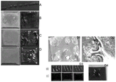
fig. 1 depicts optical micrographs of copper traces formed from an ink containing copper precursor molecules before and after soldering. A is free of copper nanoparticles and free of polymeric binders; b has 0.4 wt% copper nanoparticles and no polymer binder; c copper free nanoparticles and having 0.3 wt% RokrapolTM7075 a polyester binder; and D has 0.4 wt% copper nanoparticles and has 0.3 wt% RokrapolTM7075 polyester binder, all wt% based on the total weight of the ink.
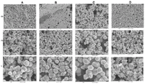
Fig. 2 depicts a Scanning Electron Microscope (SEM) image showing the topography of the unsoldered copper traces depicted in fig. 1 on a scale of 20 μm, 10 μm, and 6 μm (top row to bottom row).
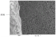
Fig. 3 depicts a Scanning Electron Microscope (SEM) image showing the topography of the soldered copper traces produced by molecular ink D depicted in fig. 1.
Detailed Description
The ink includes a mixture of copper nanoparticles, copper precursor molecules, and a polymeric binder including a polyester, a polyimide, a polyetherimide, or any mixture thereof, having surface functional groups that render the polymeric binder compatible and/or soluble with the diol.
Copper nanoparticles (CuNPs) are copper particles having an average size along the longest dimension in the range of about 1-1000nm, preferably about 1-500nm, more preferably about 1-100 nm. The copper nanoparticles may be in the form of a sheet, a wire, a needle, a substantially spherical shape, or any other shape. The copper nanoparticles may be formed by natural processes or by chemical synthesis, and are generally commercially available. The copper nanoparticles are preferably present in the ink in an amount of about 0.04 to 7 wt%, based on the total weight of the ink. More preferably, the amount of copper nanoparticles is in the range of about 0.1 to 6 wt%, or about 0.25 to 5wt%, or about 0.4 to 4wt%, or about.
The copper precursor molecule is a copper-containing compound that decomposes under sintering conditions to produce additional copper nanoparticles in the conductive copper trace. The copper precursor molecule can be an inorganic compound (e.g., CuSO)4、CuCl2、Cu(NO3)、Cu(OH)2) Ketone metal-organic compounds (copper-MOD) or mixtures thereof. copper-MOD includes, for example, copper carboxylates (e.g., C)1-C12Copper salts of alkanoic acids such as copper formate, copper acetate, copper propionate, copper butyrate, copper decanoate, copper neodecanoate, etc., copper amines (e.g., copper (II) bis (2-ethyl-1-hexylamine) formate, copper (II) bis (octylamine) formate, copper (II) tris (octylamine) formate, etc.), copper ketone complexes (e.g., (acetylacetone) copper, (trifluoroacetylacetone) copper, (hexafluoroacetylacetone) copper, (dipivaloylmethane) copper, etc.), copper (II) hydroxide-alkanolamine complexes (e.g., Cu (OH)2Ethanolamine, Cu (OH)2Diethanolamine, Cu (OH)2Triethanolamine, etc.), copper (II) -alkanolamine formate complexes and copper-amine glycol complexes (e.g., 3-diethylamino-1, 2-propanediol (DEAPD), 3- (dimethylamino) -1, 2-propanediol (DMAPD), 3-methylamino-1-2-propanediol (MPD), 3-ammonia1, 2-propanediol (APD), 3-morpholino-1, 2-propanediol, etc.).
Copper amine diol complexes are particularly preferred copper precursor molecules. Many copper amine diol complexes are liquids at ambient temperature and can act as copper precursor molecules and solvents. In addition, the copper amine glycol complex interacts favorably with the polymeric binder, resulting in excellent conductive copper traces in terms of conductivity, mechanical strength, and solderability. Particularly preferred copper amine glycol complexes are copper formate amine glycol complexes. In one embodiment, the copper amine diol complex comprises a compound of formula (I):

wherein R is1、R2、R3And R4Are the same or different and are NR5R6(R’(OH)2) or-O- (CO) -R', and R1、R2、R3Or R4At least one of them being NR5R6(R’(OH)2) Wherein: r5And R6Independently of each other is H, C1-8Linear, branched or cyclic alkyl, C2-8Straight, branched or cyclic alkenyl, or C2-8Straight, branched or cyclic alkynyl; r' is C2-8Linear, branched or cyclic alkyl; and R' is H or C1-8Linear, branched or cyclic alkyl.
In the compounds of formula (I), NR5R6(R’(OH)2) By NR5R6(R’(OH)2) The nitrogen atom of (2) is coordinated to the copper atom. On the other hand, -O- (CO) -R "is covalently bonded to the copper atom via an oxygen atom. Preferably, R1、R2、R3Or R4One or two of which are NR5R6(R’(OH)2) More preferably, R1、R2、R3Or R4Two of (A) are NR5R6(R’(OH)2)。
Preferably, R5And R6Independently is H or C1-8Straight-chain branched or cyclic alkyl, more preferably H or C1-8Straight or branched alkyl, still more preferably H or C1-4Straight or branched chain alkyl. C1-4Examples of straight-chain or branched alkyl groups are methyl, ethyl, n-propyl, isopropyl, n-butyl, sec-butyl and tert-butyl. In a particularly preferred embodiment, R5And R6Is H, methyl or ethyl.
Preferably, R' is C2-8Straight or branched alkyl, more preferably C2-5Straight or branched chain alkyl. R' is preferably a straight-chain alkyl group. In a particularly preferred embodiment, R' is propyl. On a given R' substituent, the OH groups are preferably not bonded to the same carbon atom.
Preferably, R' is H or C1-4Straight chain alkyl, more preferably H.
The copper precursor compound provides the balance of the ink weight after taking into account the copper nanoparticles, the polymeric binder, and any other inclusions in the ink. The copper precursor compound is preferably present in the ink in an amount of about 35 wt% or more based on the total weight of the ink. The amount of copper precursor compound may be about 45 wt% or more, or about 50 wt% or more, or about 55 wt% or more, or about 60 wt% or more, or about 65 wt% or more, or about 70 wt% or more, or about 75 wt% or more, or about 80 wt% or more, or about 84wt% or more. In one embodiment, the amount of copper precursor is about 84 wt%.
The polymeric binder comprises a polyester, a polyimide, a polyetherimide, or any mixture thereof, having surface functional groups such that the polymeric binder is compatible with and/or soluble in the diol. Preferably, the surface functional groups include polar groups capable of participating in hydrogen bonds. The surface functional groups preferably include one or more of hydroxyl, carboxyl, amino and sulfonyl. The polymeric binder can be present in the ink in any suitable amount. The polymeric binder is preferably present in the ink in an amount of about 0.04 to 0.8 wt%, based on the total weight of the ink. More preferably, the amount of polymeric binder is in the range of about 0.08-0.6 wt%, even more preferably about 0.25-1wt%, still even more preferably about 0.25-0.4 wt%, for example about 0.3 wt%.
The polymeric binder preferably comprises a polyester. Suitable polyesters are commercially available or may be prepared by condensation of a polyol with a polycarboxylic acid and its respective anhydride. Preferred polyesters are hydroxyl and/or carboxyl functionalized. The polyesters may be linear or branched. Solid or liquid polyesters and various solution forms may be used. In a particularly preferred embodiment, the polymeric binder comprises a hydroxyl and/or carboxyl terminated polyester, for example, RokrapolTM7075。
The polymeric binders described herein, especially surface functionalized polyesters, provide good solubility in glycols and good mechanical strength compared to other polymeric binders such as hydroxycellulose, polyphenols and polyvinylpyrrolidone. Thus, the polymeric binders described herein are particularly suitable for use with copper amine glycol complexes when the copper amine glycol complex is used as a copper precursor compound and solvent. The interaction between the polymeric binder described herein together with the copper amine diol complex and the copper nanoparticles results in conductive copper traces with particularly improved conductivity, mechanical strength and solderability.
In a particularly preferred embodiment, a screen printable copper ink comprising copper nanoparticles, a copper formate-amine diol complex and a hydroxyl and/or carboxyl terminated polyester binder provides conductive copper traces with particularly improved conductivity, mechanical strength and solderability. Copper formate amine diol complexes also provide robustness to sintering in the presence of up to 500ppm oxygen. The resulting sintered conductive copper traces have improved air stability and greater stability to lead-free soldering.
The ink may be formulated by mixing together copper nanoparticles, copper precursor molecules and a polymeric binder. The mixing may be carried out with or without additional solvent. Preferably, the copper precursor molecules are liquid and can also be used as a solvent in addition to being a precursor for copper metal formation. However, in some embodiments, additional solvents may be required. The additional solvent may include at least one aqueous solvent, at least one aromatic organic solvent, at least one non-aromatic organic solvent, or any mixture thereof, such as water, toluene, xylene, anisole, diethylbenzene, alcohols (e.g., methanol, ethanol), glycols (e.g., ethylene glycol), triols (e.g., glycerol), or any mixture thereof. The additional solvent may comprise from about 0.5 to about 50 weight percent of the ink, more preferably from about 1 to about 20 weight percent, based on the total weight of the ink.
In a preferred embodiment, the copper precursor molecule is a copper amine diol complex in liquid form. Thus, the copper amine glycol complex acts as a solvent as well as a copper precursor molecule. As previously mentioned, the use of a copper amine glycol complex as both a copper precursor molecule and a solvent is particularly advantageous because the interaction between the polymeric binder and the copper amine glycol complex results in a particularly improved conductive copper trace. However, in some embodiments, it may still be necessary to add additional solvents to the ink, for example, diols or triols. The additional diol or triol may include, for example, methyl glycol, ethylene glycol, propane-1, 2-diol, propane-1, 3-diol, glycerol, or any mixture thereof. When additional solvents are required, glycerol is preferred. In addition to the copper amine diol complex, the diol or triol is preferably used in an amount in the range of about 0.1 to 5wt%, more preferably about 0.5 to 3 wt%, for example about 1.25 wt%, based on the total weight of the ink.
Although the ink may be formulated for any kind of deposition, the ink is particularly suitable for screen printing. In this regard, the ink preferably has a viscosity of about 1,500cP or more, more preferably about 1,500-10,000cP or 4,000-8,000cP, for example, about 6,000 cP.
The ink may be deposited (e.g., printed) onto a substrate to form ink traces on the substrate. Drying the ink and decomposing the copper precursor molecules within the traces to form conductive solderable copper traces may be accomplished by any suitable technique, where the technique and conditions depend on the type of substrate on which the traces are deposited. For example, drying the ink and decomposing the copper precursor molecules can be accomplished by heating and/or photonic sintering.
In one technique, a heated substrate dries and sinters the traces to form conductive copper traces. In addition to the copper nanoparticles present in the original ink, sintering decomposes the copper precursor molecules to form conductive nanoparticles of copper present in the copper traces. The heating is preferably performed at a temperature in the range of about 110 ℃ to about 250 ℃, for example, about 130 ℃ to about 230 ℃. The heating is preferably carried out for a time period of about 2 hours or less, more preferably about 15 minutes or less, for example about 1 to 15 minutes, or about 2 to 15 minutes, particularly a time period in the range of about 3 to 10 minutes. The heating is performed at a sufficient balance of temperature and time to sinter the traces on the substrate to form conductive copper traces. The type of heating device also affects the temperature and time required for sintering. The substrate may be sintered under an inert atmosphere (e.g., nitrogen and/or argon) or a reducing atmosphere (e.g., hydrogen). It is particularly noteworthy, however, that the copper-based inks of the present invention are more robust to the presence of oxidizing agents than the control copper-based inks, and, therefore, can be sintered in the presence of oxidizing agents (e.g., air and/or oxygen). In one embodiment, the oxygen content of the sintering atmosphere may be up to about 500 ppm. Furthermore, the sintered copper traces exhibit improved air stability.
In another technique, the photonic sintering system may feature a high intensity lamp (e.g., a pulsed xenon lamp) that provides a broadband spectrum. The lamp may provide about 5-20J/cm to the trace2The energy of (a). The pulse width is preferably in the range of about 0.58-1.5 ms. The drive voltage is preferably in the range of about 2.0-2.8 kV. Photonic sintering may be performed under ambient conditions (e.g., in air). The photonic sintering can be performed using milder conditions compared to copper inks that include a copper organic compound but do not include copper nanoparticles. Photonic sintering is particularly suitable for, but not limited to, polyethylene terephthalate and polyimide substrates.
The ink may be deposited on the substrate by any suitable method (e.g., printing). Printing includes, for example, screen printing, ink jet printing, flexographic printing (e.g., stamping), gravure printing, offset printing, spray coating, aerosol printing, typesetting, or any other method. After deposition, the ink may be dried and/or sintered, for example, by allowing the ink to dry and/or heating the ink for an appropriate amount of time under ambient conditions. The inks of the invention are particularly suitable for screen printing. The ink can be used in other printing processes by appropriately adjusting the viscosity of the ink.
The substrate (substrate) may be any suitable surface, in particular any printable surface. Printable surfaces can include, for example, polyethylene terephthalate (PET) (e.g., Melinex)TM) Polyolefins (e.g., silica-filled polyolefins (Teslin)TM) Polydimethylsiloxane (PDMS), polystyrene, polycarbonate, polyetherimide (e.g., Ultem)TM) Polyimide (e.g., Kapton @)TM) Silicone films, printed wiring board substrates (e.g., woven fiberglass cloth with epoxy resin binder (FR 4)), fabrics (e.g., cellulose fabrics), Thermoplastic Polyurethane (TPU), paper, glass, metal, dielectric coatings, and the like. A flexible substrate is preferred. The substrate preferably comprises polyethylene terephthalate (PET) or polyimide.
Conductive copper traces made from the inks of the present invention preferably have a sheet resistivity of about 250mOhm/sq/mil or less, more preferably about 100mOhm/sq/mil or less, even more preferably about 80mOhm/sq/mil or less, even more preferably about 65mOhm/sq/mil or less, and even more preferably about 35mOhm/sq/mil or less. The sheet resistivity of conductive copper traces made with the inks of the present invention can be 10% or more lower than the sheet resistivity of conductive copper traces made with the comparative prior inks. In some cases, the sheet resistivity may be 15% or less lower, or even 20% or less lower.
Conductive copper traces made from the inks of the present invention perform well in standard ASTM bend and crease tests (ASTM F1683-02) for flexibility while maintaining high conductivity. In a preferred embodiment, the conductive trace can maintain a change in resistivity (conductivity) of about 15% or less, preferably about 10% or less, more preferably about 5% or less, even more preferably about 3% or less after 10 compression bending or 10 tensile bending cycles, according to ASTM test F1683-02. In another preferred embodiment, the conductive traces can maintain a change in resistivity (conductivity) of about 20% or less, preferably about 15% or less, more preferably about 10% or less, and still more preferably about 5% or less after 1 compression creping or 1 tension creping cycle according to ASTM test F1683-02.
The conductive copper traces preferably have a thickness of about 4 microns or less, preferably about 2 microns or less. The conductive copper traces preferably have a nominal line width of about 2 mils or greater, more preferably about 3 mils or greater, and even more preferably about 5 mils or greater. Preferably, the nominal line width is about 20 mils or less. There may be a trade-off between line thickness/width and sheet resistivity/mechanical strength/solderability (trade-off). In some cases, thinner and/or narrower copper traces may result in higher sheet resistivity, poorer mechanical strength, and/or poorer solderability.
Generally, for a given line thickness/width, conductive copper traces made from the inks of the present invention have lower sheet resistivity, better mechanical strength, and/or better solderability than conductive copper traces made from the control inks. In one embodiment, sheet resistivities in the range of about 20-30mOhm/sq/mil can be obtained for screen printed conductive copper traces with good resolution at nominal line widths in the range of about 5-20 mil.
Substrates having conductive solderable copper traces thereon can be incorporated into electronic devices such as circuits, conductive bus bars (bus bars) (e.g., for photovoltaic cells), sensors (e.g., touch sensors, sensor arrays), antennas (e.g., RFID antennas), thin film transistors, diodes, and smart packaging (e.g., smart pharmaceutical packaging).
The sintered copper traces are conductive and solderable. The copper traces may be electrically and thermally conductive. For use in electronic applications, the copper traces are desirably at least electrically conductive. The sintered copper traces are advantageously solderable directly without the use of a lead-containing solder to form electrical connections between electronic components on the substrate. It is believed that the copper traces can be soldered with lead-free solder due, at least in part, to excellent wettability. The soldered copper traces had better adhesion strength and comparable or better conductivity than copper traces formed from the control copper ink. Furthermore, the copper-based inks of the present invention not only can increase the conductivity of the sintered copper traces, but surprisingly can also achieve excellent oxidation resistance. Thus, the copper-based inks of the present invention can unexpectedly provide conductive copper traces with direct solderability and long-term storage stability, as well as with increased conductivity and mechanical strength.
Example (b):
example 1: copper nanoparticle (CuNP) pair consisting of CuF: DEAPD and RokrapolTM7075 Binder formulated ink effects on conductivity of copper (Cu) traces
By mixing 0 wt% or 0.4 wt% of CuNP (TEKNA from Advanced materials Inc.)TM) And 0.3 wt% carboxyl terminated polyester binder (Rokrapol from Kramer)TM7075) Mixed in CuF: DEADD (1:1mol eq Cu: DEADD) and includes 3mol eq water (H)2O) (based on moles CuF: DEAPD) and 1.25 wt% glycerol as additional solvents. CuF DEAPD was formed from copper formate hydrate (STREM Chemicals, Inc.) and 3- (diethylamino) -1-2-propanediol (Aldrich). Screen printing of ink onto KaptonTMInk traces on the film to produce the same length (10cm) and various nominal line widths, as shown in tables 1 and 2. The ink traces were sintered at 110 ℃ for 30min, then at 210 ℃ for 5min, and then at 230 ℃ for 5min (substrate temperature) under a nitrogen atmosphere containing 500ppm oxygen.
TABLE 1

0wt%CuNP
TABLE 2


0.4wt%CuNP
As is apparent from tables 1 and 2, with anhydrous copper (II) formate 3Diethylamino-1, 2-propanediol (CuF: DEAPD), copper nanoparticles (CuNP) and RokrapolTM7075 the combination of polyester binders formulated inks provide screen printed copper traces with excellent line resolution and high conductivity (low resistivity).
Example 2: effect of copper nanoparticle (CuNP) Loading in inks formulated with Anhydrous copper (II) formate 3-diethylamino-1, 2-propanediol (CuF: DEAPD)
By mixing 0, 0.4, 0.8 or 4.1 wt% of copper nanoparticles based on the total weight of the ink into CuF: DEADD (1:1mol eq Cu: DEADD) and including 2.5mol eq water (H)2O) (based on moles CuF: DEAPD) and 1.25 wt% glycerol as additional solvents. Printing ink to Kapton using ribbon mask technologyTMOn the film to produce ink traces of the same length (10cm) with nominal line widths in the range of about 20-40 mils. The ink traces were sintered at 130 ℃ for 5min, then 190 ℃ for 5min, and then 210 ℃ for 5min (substrate temperature) under a nitrogen atmosphere containing 500ppm oxygen. As is apparent from table 3, the addition of copper nanoparticles increases the conductivity (lowers the resistivity) of the sintered copper traces at relatively low loadings. Furthermore, as the loading of copper nanoparticles increased to about 4.1 wt%, the copper traces were difficult to adhere to the substrate, indicating the need for a binder.
TABLE 3
| CuNP(wt%) | Resistance (omega) |
| 0 | 43-49 |
| 0.4 | 13-17 |
| 0.8 | 17-19 |
| 4.1 | 47-67 |
Example 3: effect of copper nanoparticles (CuNP) on the conductivity of copper traces prepared from inks formulated with CuF: DEAPD and screen printed on different substrates
In KaptonTMOn the upper part
By mixing 0 wt%, 0.4 wt% or 0.6 wt% of copper nanoparticles into CuF: DEAPD (1:1mol eq Cu: DEAPD) and including 2.5 or 3mol eq water (H)2O) (based on moles CuF: DEAPD) and 1.25 wt% glycerol as additional solvents molecular inks were formulated. Screen printing of ink onto KaptonTMInk traces on the film to produce the same length (10cm) and various nominal line widths as shown in tables 4, 5, 6, 7 and 8. The ink traces were sintered at 130 ℃ for 3min or 30min, then 190 ℃ or 210 ℃ for 5min, and then 230 ℃ for 5min (substrate temperature) under a nitrogen atmosphere containing 500ppm oxygen.
TABLE 4

0wt%CuNP、2.5eq H2O, 130 ℃ for 3min, then 210 ℃ for 5min, then 230 ℃ for 5min
TABLE 5

0.6wt%CuNP、2.5eq H2O at 130 deg.C for 3min, then at 210 deg.C for 5min, then at 230 deg.C for 5min
The addition of copper nanoparticles to the ink helped to produce screen printed high resolution copper traces with increased conductivity, as shown in tables 4 and 5. Moreover, the addition of copper nanoparticles shows enhanced oxidation resistance to the sintered copper traces over time. The resistivity of the ink without copper nanoparticles increased by 200% within one month; whereas inks containing copper nanoparticles showed a 20% increase in resistivity in one month.
TABLE 6

0.4wt%CuNP、3eq H2O at 130 deg.C for 3min, then at 210 deg.C for 5min, then at 230 deg.C for 5min
TABLE 7

0.4wt%CuNP、3eq H2O at 130 deg.C for 30min, then at 210 deg.C for 5min, then at 230 deg.C for 5min
TABLE 8

0.4wt%CuNP、3eq H2O at 130 deg.C for 30min, then at 190 deg.C for 5min, then at 230 deg.C for 5min
As is apparent from tables 6, 7 and 8, the sintering conditions can be optimized to be in KaptonTMResulting in sintered copper traces with excellent resolution and even higher conductivity for lines having nominal widths in the range of 2-20 mils.
In MelinexTMOn the upper part
Using MelinexTMAs a substrate rather than KaptonTMSimilar experiments were performed. MelinexTMIs a low-temperature matrix, so the sintering condition is mild. Thus, by0 wt% or 0.4 wt% of copper nanoparticles are mixed into CuF: DEAPD (1:1mol eq Cu: DEAPD) and 2.5mol eq water (H)2O) (based on moles CuF: DEAPD) and 1.25 wt% glycerol as additional solvents molecular inks were formulated. Screen printing of ink onto MelinexTMInk traces on the film to produce the same length (10cm) and various nominal line widths as shown in tables 9 and 10. The ink traces were sintered at 130 ℃ for 60min and then at 145 ℃ for 10min (substrate temperature) under a nitrogen atmosphere containing 500ppm oxygen.
TABLE 9

0wt%CuNP
Watch 10

0.4wt%CuNP
It is apparent from tables 9 and 10 that conductive traces with good resolution can be screen printed to MelinexTMAnd the addition of copper nanoparticles increases the conductivity.
Example 4: the photo-sintered pair is prepared by using CuF: DEAPD with or without copper nanoparticles (CuNP) and RokrapolTM7075 Binder formulation ink Effect of Screen printed Cu traces
By mixing 0 wt% or 0.4 wt% copper nanoparticles and 0 wt% or 0.3 wt% carboxyl terminated polyester binder (Rokrapol)TM7075) Mixed in CuF: DEADD (1:1mol eq Cu: DEADD) and includes 3mol eq water (H)2O) (based on moles CuF: DEAPD) and 1.25 wt% glycerol as additional solvents molecular inks were formulated. Screen printing of ink onto KaptonTMInk traces on the film to produce the same length (10cm) and various nominal line widths as shown in tables 11, 12 and 13. The ink traces were photosintered in air at either 2.6eV or 2.4eV under PFN 2. PFN2 is the pulse width, pulse forming network stage 2. There are four PFsThe N-phases, the connections to these different phases allow different pulse durations and single pulse energies to be configured.
TABLE 11

0wt%CuNP,0wt%RokrapolTM7075、2.5eV
TABLE 12

0wt%CuNP、0wt%RokrapolTM7075、2.6eV
Watch 13

0.4wt%CuNP、3.75wt%RokrapolTM7075、2.4eV
TABLE 14

0.6wt%CuNP、3.75wt%RokrapolTM7075、2.4eV
As is apparent from tables 11 to 14, the resistance of the Cu traces decreased significantly with the addition of the copper nanoparticles, and the traces could also be sintered under milder photosintering conditions.
Example 5: mechanical Properties of Screen-printed copper traces made from inks
By mixing 0.6 wt% copper nanoparticles and 0.3 wt% carboxyl terminated polyester binder (Rokrapol)TM7075) Mixed in CuF: DEADD (1:1mol eq Cu: DEADD) and includes 3mol eq water (H)2O) (based on moles CuF: DEAPD) and 1.25 wt% glycerol as additional solvents molecular inks were formulated. Screen printing of ink onto KaptonTMInk traces on the film to produce the same length (10cm) and various nominal line widths as shown in tables 15 and 16. The ink traces in table 15 were photo-sintered in air at 2.4eV under PFN 2. The ink traces in table 16 were thermally sintered at 110 ℃ for 30min, then 210 ℃ for 5min, and then 230 ℃ for 5min (substrate temperature) under a nitrogen atmosphere containing 500ppm oxygen. Tables 15 and 16 provide the mechanical properties of the photo-sintered copper traces and the thermally sintered copper traces, respectively.
As is apparent from table 15, the photo-sintered copper traces prepared with CuNP, CuF: DEAPD and polymer binder passed all mechanical tests with the resistivity (R) maintained within acceptable limits without physical destruction of the trace, i.e., without open circuit failure. As shown in table 16, the thermally sintered copper traces with nominal line widths from 20mil to 3mil passed all mechanical tests, except for tensile bending, the resistivity (R) remained within acceptable limits, and no open circuit failure occurred. Thermally sintered copper traces with a nominal line width of 2 mils failed in all mechanical tests, indicating that photo sintering is the preferred sintering method for copper traces with nominal line widths below 3 mils.
Watch 15

0.6wt%CuNP、3.75wt%RokrapolTM7075
TABLE 16

0.6wt%CuNP、3.75wt%RokrapolTM7075
Using a binder (Rokrapol) with and/or without copper nanoparticlesTM7075) The photo-sintered traces prepared with the ink of (a) failed all ASTM standard mechanical tests. However, the addition of binder to inks that do not contain nanoparticles passed ASTM standard mechanical testing, as shown in Table 17. These results demonstrate that the incorporation of binder provides good mechanical properties.
TABLE 17

0.0wt%CuNP、3.75wt%RokrapolTM7075
Example 6: solderability of screen printed copper traces made from inks
Molecular inks were formulated in CuF: DEADD (1:1mol eq Cu: DEADD) containing 3mol eq water (H)2O) (based on moles CuF: DEAPD) and 3 wt% glycerol as additional solvents as follows:
A. with 0 wt% copper nanoparticles and 0 wt% RokrapolTM7075。
B. With 0.4 wt% copper nanoparticles.
C. With 0.3 wt% RokrapolTM7075。
D. With 0.4 wt% copper nanoparticles and 0.3 wt% RokrapolTM7075。
Printing ink to Kapton using ribbon mask technologyTMOn the film to produce ink traces of the same length (10cm) having a width in the range of about 20-40 mils. The ink traces were sintered at 130 ℃ for 30min, then at 210 ℃ for 5min, and then at 230 ℃ for 5min (substrate temperature) under a nitrogen atmosphere containing 500ppm oxygen.
The hand-held soldering iron was used for soldering using a lead-free solder wire 97SC/SAC305 (96.5% Sn, 3% Ag, 0.5% Cu, melting point 217 ℃). The soldering iron tip temperature is about 330 ℃. The copper traces were cleaned using a flux paste (MG chemical 8341).
As shown in fig. 1, the copper traces produced by molecular inks A, B and C cannot be soldered directly. For the copper traces produced by molecular inks a and B, the solder dissolves in the copper traces and does not wet the surface of the copper traces. The resistances were 43-49 Ω and 13-17 Ω, respectively, for the copper traces produced by molecular inks a and B. For copper traces produced from molecular ink C, the solder wets the surface of the trace but does not adhere. Further, the resistance of the traces produced by molecular ink C was 200-250 Ω.
However, as shown in fig. 1, the copper traces produced by molecular ink D may be soldered directly. Referring to D1, D2, D3, and D4 in fig. 1, the solder wets the surface of the trace and adheres well (D1 and D2), does not dissolve copper (D3), and forms a stronger copper pad (D4).
Fig. 2 further illustrates the topography of the unsoldered copper trace depicted in fig. 1. As is evident from fig. 2, the copper traces produced by molecular ink D have a smooth and robust surface compared to the copper traces produced by molecular inks A, B and C. In addition, as is evident in fig. 3, the solder joint on the copper trace produced by molecular ink D is strong, free of cracking, no peeling, and no flaking of the copper trace.
Example 7: other polymeric binders
Control inks including copper nanoparticles (CuNP) and anhydrous copper (II) formate (CuF: DEAPD) were formulated using other polymeric binders to evaluate the properties of the control inks. As is evident from the results shown below, the choice of polymeric binder is important for formulating inks that can produce conductive copper traces with direct solderability and long term storage stability, with enhanced conductivity and mechanical strength.
PhenalloyTM2870
PhenalloyTM2870 (from Dynachem) is a phenolic resin in ethanol solution with a viscosity of 2000cp and a solids content of 70%.
In a similar manner to that described above by mixing 0.4 wt% CuNP and 0.3 wt% PhenalloyTM2870 in CuF: DEADD (1:1mol eq Cu: DEADD) and includes 3mol eq water (H)2O) (based on moles CuF: DEAPD) and 1.25 wt% glycerol as additional solvents molecular inks were formulated. Screen printing of ink onto KaptonTMInk traces were generated on the film to produce the same length (10cm) and various nominal line widths, as shown in table 16. The ink traces were sintered at 110 ℃ for 30min, then at 230 ℃ for 5min, and then at 250 ℃ for 5min (substrate temperature) under a nitrogen atmosphere containing 500ppm oxygen. As shown in Table 18, Phen was usedalloyTM2870 the copper traces have a chemical composition similar to that of RokrapolTM7075 the prepared traces have similar conductivity.
However, by PhenalloyTM2870 the resulting sintered copper traces oxidize faster, i.e., almost instantaneously turn black, and fail in both the standard ASTM bend and crease test for flexibility (ASTM F1683-02).
Watch 18

Poly (vinyl alcohol)
Poly (vinyl alcohol) was tested as the polymer binder for the ink formulations of the present invention. Although the polymer was soluble in amine diol (3- (diethylamino) -1-2-propanediol (DEAPD)), the introduction of copper formate hydrate into the mixture resulted in precipitation. The corresponding copper ink formulated with 0.12 wt% polymer did not produce copper traces on the substrate upon sintering.
Poly (styrenesulfonic acid)
Poly (styrene sulfonic acid) was tested as the polymer binder for the ink formulations of the present invention. However, the polymer was found to be insoluble in amine diol (3- (diethylamino) -1-2-propanediol (DEAPD)), and insoluble in a mixture of copper formate hydrate and amine diol. The corresponding copper ink formulated with 0.12 wt% polymer did not produce copper traces on the substrate upon sintering.
Chitosan
Chitosan was tested as the polymer binder for the ink formulations of the present invention. However, the polymer was found to be insoluble in amine diol (3- (diethylamino) -1-2-propanediol (DEAPD)), and insoluble in a mixture of copper formate hydrate and amine diol. The corresponding copper ink formulated with 0.12 wt% polymer did not produce copper traces on the substrate upon sintering.
Poly (ethylene glycol) MN200
Poly (ethylene glycol) MN200 was tested as the polymer binder for the ink formulations of the present invention. Although the polymer was soluble in amine diol (3- (diethylamino) -1-2-propanediol (DEAPD)) and a mixture of copper formate hydrate and amine diol, the corresponding copper ink formulated with 0.12 wt% polymer produced only discontinuous non-conductive copper traces on the substrate when sintered at 210 ℃ and 250 ℃.
PEG _ silane
Silylated polyethylene glycol (PEG silane) was tested as the polymeric binder for the ink formulations of the present invention. Although the polymer was soluble in amine diol (3- (diethylamino) -1-2-propanediol (DEAPD)) and a mixture of copper formate hydrate and amine diol, the corresponding copper ink formulated with 0.12 wt% polymer produced only discrete non-conductive copper traces on the substrate when sintered at 210 ℃ and 250 ℃.
Poly (acrylic acid) sodium salt
Sodium poly (acrylate) salt was tested as the polymer binder for the ink formulations of the present invention. Although the polymer was soluble in amine diol (3- (diethylamino) -1-2-propanediol (DEAPD)) and a mixture of copper formate hydrate and amine diol, the corresponding copper ink formulated with 0.12 wt% polymer produced only discrete non-conductive copper traces on the substrate when sintered at 210 ℃ and 250 ℃. In addition, copper traces showed poor adhesion to the substrate.
Sodium salt of poly (methacrylic acid) and poly (vinyl butyral)
Poly (methacrylic acid) sodium salt and poly (vinyl butyral) were tested as the polymer binder for the ink formulations of the present invention. The polymer is soluble in amine diol (3- (diethylamino) -1-2-propanediol (DEAPD)) and a mixture of copper formate hydrate and amine diol. The corresponding copper ink formulated with 0.12 wt% polymer produced conductive copper traces, but the traces adhered poorly to the substrate.
Lignin
Lignin was tested as a polymer binder for the ink formulations of the present invention. However, the polymer was found to be insoluble in amine diol (3- (diethylamino) -1-2-propanediol (DEAPD)), and insoluble in a mixture of copper formate hydrate and amine diol. The corresponding copper ink formulated with 0.12 wt% polymer did not produce copper traces on the substrate upon sintering.
Long chains of polyaniline grafted to lignin
The long polyaniline chains grafted to lignin were tested as the polymer binder for the ink formulations of the present invention. Although the polymer was soluble in amine diol (3- (diethylamino) -1-2-propanediol (DEAPD)), the introduction of copper formate hydrate into the mixture resulted in precipitation. The corresponding copper ink formulated with 0.12 wt% polymer produced no copper traces on sintering.
Reference documents: the entire contents of each of which are incorporated herein by this reference.
Chen W,Deng D,Chenge Y,Xiao F.J.(2015)Electronics Materials.44(7),2479.
Chung W,Hwang H,Kim H.(2015)Thin Solid Films.580,61-70.
Curtis C,Rivkin T,Miedaner A,Alleman J,Perkins J,Smith L,Ginley D.(2001)NREL/CP-520-31020.
Dang Z-M,Zhang B,Li J,Zha J-W,Hu G-H.(2012)J.Applied Polymer Science.126,815.
Farraj Y,Grouchko M,Magdassi S.(2015)Chem.Commun.51,1587.
Hu Y,An B,Niu C,Lv W,Wu Y.(2014)International Conference on Electronic Packaging Technology.1565.
Lee B,Kim Y,Yang S,Jeong I,Moon J.(2009)Current Applied Physics.9,e157-e160.
Pham LQ,Sohn JH,Kim CW,Park JH,Kang HS,Lee BC,Kang YS.(2012)J.Colloid and Interface Science.365,103-109.
Schulz DL,Curtis CJ,Ginley DS.(2001)Electrochemical and Solid State Letters.4(8),C58-C61.
Shin D-H,Woo S,Yem H,Cha M,Cho S,Kang M,Jeong S,Kim Y,Kang K,Piao Y.(2014)ACS Appl.Mater.Interfaces.6,3312.
Szeremeta J,Nyk M,Chyla A,Strek W,Samoc M.(2011)Optical Materials.33,1372-1376.
Tsai C-Y,Chang W-C,Chen G-L,Chung C-H,Liang J-X,Ma W-Y,Yang T-N.(2015)Nanoscale Research Letters.10,357.
Yabuki A,Tanaka S.(2012)Mater.Res.Bull.47,4107.
Yabuki A,Tachibana Y,Fathona IW.(2014)Mater.Chem.&Phys.148,299.
United states patent 4,248,921 granted on 3.2.1981.
Us patent 4,396,666 granted on 8/2/1983.
Us patent 4,687,597 issued 8/18 1987.
United states patent 5,045,236, granted on 3/9/1991.
U.S. patent 5,248,451 issued on 9/28 1993.
United states patent 6,036,889 granted 3/14/2000.
Us patent 7,211,205 granted on 5/1/2007.
United states patent 7,731,812, granted on 6/8/2010.
Us patent 9,145,503 granted on 29/9/2015.
U.S. patent publication 2008/0108218, published 5/8/2008.
Us patent publication 2015/0257279, published on 9/10/2015.
Korean patent No. 101350507 granted on 17.1.2014.
Korean patent laid-open abstract 2012/0132424 published on 12/5/2012.
Korean patent laid-open abstract 2015/0045605 published on 29/4/2015.
Korean patent laid-open abstract 2015/0077676 published on 8/7/2015.
Korean patent laid-open abstract 2015/0082133 published on 7/15/2015.
The novel features will become apparent to those skilled in the art upon examination of the specification. It should be understood, however, that the scope of the claims should not be limited by the embodiments, but should be given the broadest interpretation consistent with the language of the claims and specification as a whole.
Claims (19)
1. An ink comprising a mixture of:
(a) copper nanoparticles;
(b) a copper precursor molecule, wherein the copper precursor molecule comprises a copper-amine diol complex; and
(c) a polymeric binder comprising a hydroxyl and/or carboxyl terminated polyester.
2. The ink of claim 1, wherein the copper-amine diol complex comprises a compound of formula (I):

wherein R is1、R2、R3And R4Are the same or different and are NR5R6(R’(OH)2) or-O- (CO) -R', and R1、R2、R3Or R4At least one of them being NR5R6(R’(OH)2) Wherein: r5And R6Independently of each other is H, C1-8Linear, branched or cyclic alkyl, C2-8Straight, branched or cyclic alkenyl, or C2-8Straight, branched or cyclic alkynyl; r' is C2-8Linear, branched or cyclic alkyl; and R' is H or C1-8Linear, branched or cyclic alkyl.
3. The ink of claim 2, wherein R1、R2、R3Or R4Two of (A) are NR5R6(R’(OH)2)。
4. The ink of claim 2, wherein R5And R6Independently is H or C1-4A linear alkyl radical, and R' is H or C1-4A linear alkyl group.
5. The ink of claim 2, wherein R "is H.
6. The ink of claim 2, wherein the OH groups on a given R' substituent are not bonded to the same carbon atom.
7. The ink of claim 1, wherein the copper precursor molecules comprise anhydrous copper (II) formate, 3-dimethylamino-1, 2-propanediol (CuF: DMAPD), anhydrous copper (II) formate, 3-diethylamino-1, 2-propanediol (CuF: DEAPPD), anhydrous copper (II) formate, 3-methylamino-1, 2-propanediol (CuF: MAPD), anhydrous copper (II) formate, 3-amino-1, 2-propanediol (CuF: APD), Cu (OH)2Ethanolamine, Cu (OH)2Diethanolamine or Cu (OH)2Triethanolamine.
8. The ink of claim 1, wherein the copper nanoparticles are present in a range of 0.25 to 5wt% based on the total weight of the ink.
9. The ink of claim 1, wherein the polymeric binder is present in a range of 0.25 to 1wt% based on the total weight of the ink.
10. The ink of claim 1, wherein the copper precursor molecules are present in a range of 84wt% or more based on the total weight of the ink.
11. A method of producing an electrically conductive solderable copper trace on a substrate, the method comprising depositing an ink as defined in any one of claims 1 to 10 on a substrate and sintering the ink on the substrate to produce an electrically conductive solderable copper trace on the substrate.
12. The method of claim 11, wherein the depositing comprises printing the ink onto the substrate.
13. The method of claim 11, wherein the depositing comprises screen printing the ink onto the substrate.
14. A substrate comprising an electrically conductive solderable copper trace produced by the method as defined in claim 11.
15. The substrate of claim 14, comprising polyethylene terephthalate (PET), polyolefin, Polydimethylsiloxane (PDMS), polystyrene, polycarbonate, polyimide, fabric, thermoplastic polyurethane, paper, glass, metal, or a dielectric coating.
16. The substrate of claim 14, comprising a silicone membrane.
17. The substrate of claim 14 comprising polyethylene terephthalate or polyimide.
18. An electronic device comprising a substrate as defined in claim 14.
19. The electronic device of claim 18, comprising a circuit, a conductive bus bar, a sensor, an antenna, a thin film transistor, a diode, or a smart package.
Applications Claiming Priority (3)
| Application Number | Priority Date | Filing Date | Title |
|---|---|---|---|
| US201662367810P | 2016-07-28 | 2016-07-28 | |
| US62/367,810 | 2016-07-28 | ||
| PCT/CA2017/050870 WO2018018136A1 (en) | 2016-07-28 | 2017-07-19 | Copper ink and conductive solderable copper traces produced therefrom |
Publications (2)
| Publication Number | Publication Date |
|---|---|
| CN109790409A CN109790409A (en) | 2019-05-21 |
| CN109790409B true CN109790409B (en) | 2022-03-04 |
Family
ID=61015482
Family Applications (1)
| Application Number | Title | Priority Date | Filing Date |
|---|---|---|---|
| CN201780059065.5A Active CN109790409B (en) | 2016-07-28 | 2017-07-19 | Copper ink and conductive solderable copper traces made therefrom |
Country Status (8)
| Country | Link |
|---|---|
| US (1) | US10844238B2 (en) |
| EP (1) | EP3491082B1 (en) |
| JP (1) | JP6901549B2 (en) |
| KR (1) | KR102360657B1 (en) |
| CN (1) | CN109790409B (en) |
| CA (1) | CA3032252A1 (en) |
| TW (1) | TWI752986B (en) |
| WO (1) | WO2018018136A1 (en) |
Families Citing this family (8)
| Publication number | Priority date | Publication date | Assignee | Title |
|---|---|---|---|---|
| CN112789331A (en) * | 2018-08-03 | 2021-05-11 | 加拿大国家研究委员会 | UV sinterable molecular inks and processing thereof using broad spectrum UV light |
| WO2020076326A1 (en) * | 2018-10-11 | 2020-04-16 | Hewlett-Packard Development Company, L.P. | Generation of metals in textiles |
| JP7269565B2 (en) * | 2019-03-29 | 2023-05-09 | 学校法人 関西大学 | Conductive ink composition and conductive laminate |
| KR102213925B1 (en) * | 2019-10-31 | 2021-02-08 | (주)쎄미시스코 | Ink composition for flash light sintering comprising silica particles |
| CN111269615A (en) * | 2020-03-20 | 2020-06-12 | 辽宁大学 | Antioxidant particle-free copper conductive ink and preparation method thereof |
| CN114799613B (en) * | 2021-01-28 | 2023-11-07 | 深圳先进电子材料国际创新研究院 | Copper paste and preparation method and application thereof |
| CN114231092A (en) * | 2021-12-15 | 2022-03-25 | 深圳先进技术研究院 | Copper conductive ink, flexible substrate and preparation method of flexible substrate |
| CN114540889B (en) * | 2022-03-25 | 2023-03-24 | 江阴纳力新材料科技有限公司 | Copper plating additive, copper plating solution and application thereof |
Citations (1)
| Publication number | Priority date | Publication date | Assignee | Title |
|---|---|---|---|---|
| CN103382327A (en) * | 2012-05-02 | 2013-11-06 | 比亚迪股份有限公司 | Copper ink for solar cell, preparation method of the copper ink, manufacturing method of solar cell main grid, and solar cell module |
Family Cites Families (25)
| Publication number | Priority date | Publication date | Assignee | Title |
|---|---|---|---|---|
| DE2728465C2 (en) | 1977-06-24 | 1982-04-22 | Preh, Elektrofeinmechanische Werke, Jakob Preh, Nachf. Gmbh & Co, 8740 Bad Neustadt | Printed circuit |
| US4396666A (en) | 1981-11-02 | 1983-08-02 | Cts Corporation | Solderable conductive employing an organic binder |
| US4687597A (en) | 1986-01-29 | 1987-08-18 | E. I. Du Pont De Nemours And Company | Copper conductor compositions |
| JPH01168867A (en) * | 1987-12-24 | 1989-07-04 | Mitsubishi Gas Chem Co Inc | Production of article coated with copper film |
| JP2619289B2 (en) | 1989-06-20 | 1997-06-11 | 三井金属鉱業株式会社 | Copper conductive composition |
| JP2660937B2 (en) | 1990-07-16 | 1997-10-08 | 三井金属鉱業株式会社 | Copper conductive composition |
| US5882722A (en) | 1995-07-12 | 1999-03-16 | Partnerships Limited, Inc. | Electrical conductors formed from mixtures of metal powders and metallo-organic decompositions compounds |
| US20030148024A1 (en) | 2001-10-05 | 2003-08-07 | Kodas Toivo T. | Low viscosity precursor compositons and methods for the depositon of conductive electronic features |
| US7211205B2 (en) | 2003-01-29 | 2007-05-01 | Parelec, Inc. | High conductivity inks with improved adhesion |
| US7731812B2 (en) | 2004-10-19 | 2010-06-08 | E.I. Du Pont De Nemours And Company | Thick film conductor case compositions for LTCC tape |
| US8017044B2 (en) | 2008-07-08 | 2011-09-13 | Xerox Corporation | Bimodal metal nanoparticle ink and applications therefor |
| KR101276237B1 (en) | 2010-12-02 | 2013-06-20 | 한국기계연구원 | Low sintering temperatures Conducting metal layer and the preparation method thereof |
| TWI532059B (en) * | 2011-03-31 | 2016-05-01 | Taiyo Holdings Co Ltd | Conductive paste, conductive pattern formation method and conductive pattern |
| KR20120132424A (en) | 2011-05-27 | 2012-12-05 | 한양대학교 산학협력단 | Light sintering method of conductive Cu nano ink |
| JP5821551B2 (en) * | 2011-11-10 | 2015-11-24 | 日立化成株式会社 | Conductive particles, anisotropic conductive materials, and conductive connection structures |
| WO2013128449A2 (en) | 2012-02-29 | 2013-09-06 | Yissum Research Development Company Of The Hebrew University Of Jerusalem Ltd | Inks containing metal precursors nanoparticles |
| KR20140044743A (en) | 2012-10-04 | 2014-04-15 | 한양대학교 산학협력단 | Conductive hybrid cu ink and light sintering method using the same |
| KR101350507B1 (en) | 2013-01-09 | 2014-01-17 | (주)쎄미시스코 | Electro-conductive ink comprising metal nano-particle and light sintering method of the same |
| JP2014182913A (en) | 2013-03-19 | 2014-09-29 | Fujifilm Corp | Composition for conductive film formation, and method for producing conductive film using the same |
| JP2014196427A (en) | 2013-03-29 | 2014-10-16 | 富士フイルム株式会社 | Composition for forming an electroconductive film and method for manufacturing electroconductive film using the same |
| KR20150045605A (en) | 2013-10-21 | 2015-04-29 | 전자부품연구원 | Composition for copper ink and method for forming conductive pattern using the same |
| KR101597651B1 (en) | 2013-12-30 | 2016-02-25 | 전자부품연구원 | Nano copper oxide ink composition with high heat resistance and manufacturing method of electrode using the same |
| EP2918371A1 (en) | 2014-03-11 | 2015-09-16 | Heraeus Precious Metals North America Conshohocken LLC | Solderable conductive polymer thick film composition |
| KR20150134728A (en) * | 2014-05-22 | 2015-12-02 | 주식회사 동진쎄미켐 | Conductive composition |
| JP2016029638A (en) * | 2014-07-15 | 2016-03-03 | 東洋インキScホールディングス株式会社 | Conductive paste for laser machining |
-
2017
- 2017-07-19 WO PCT/CA2017/050870 patent/WO2018018136A1/en unknown
- 2017-07-19 US US16/321,076 patent/US10844238B2/en active Active
- 2017-07-19 CA CA3032252A patent/CA3032252A1/en active Pending
- 2017-07-19 EP EP17833137.7A patent/EP3491082B1/en active Active
- 2017-07-19 CN CN201780059065.5A patent/CN109790409B/en active Active
- 2017-07-19 JP JP2019504746A patent/JP6901549B2/en active Active
- 2017-07-19 KR KR1020197005617A patent/KR102360657B1/en active IP Right Grant
- 2017-07-26 TW TW106125020A patent/TWI752986B/en active
Patent Citations (1)
| Publication number | Priority date | Publication date | Assignee | Title |
|---|---|---|---|---|
| CN103382327A (en) * | 2012-05-02 | 2013-11-06 | 比亚迪股份有限公司 | Copper ink for solar cell, preparation method of the copper ink, manufacturing method of solar cell main grid, and solar cell module |
Also Published As
| Publication number | Publication date |
|---|---|
| EP3491082A4 (en) | 2020-06-03 |
| US20190177565A1 (en) | 2019-06-13 |
| EP3491082A1 (en) | 2019-06-05 |
| CN109790409A (en) | 2019-05-21 |
| KR102360657B1 (en) | 2022-02-08 |
| US10844238B2 (en) | 2020-11-24 |
| WO2018018136A1 (en) | 2018-02-01 |
| EP3491082B1 (en) | 2022-03-30 |
| TWI752986B (en) | 2022-01-21 |
| TW201815994A (en) | 2018-05-01 |
| JP2019529599A (en) | 2019-10-17 |
| CA3032252A1 (en) | 2018-02-01 |
| KR20190042586A (en) | 2019-04-24 |
| JP6901549B2 (en) | 2021-07-14 |
Similar Documents
| Publication | Publication Date | Title |
|---|---|---|
| CN109790409B (en) | Copper ink and conductive solderable copper traces made therefrom | |
| CN103339685B (en) | Conductive paste and its manufacture method | |
| WO2013018777A1 (en) | Composition set, electroconductive substrate and manufacturing method thereof, and electroconductive binding material composition | |
| US20070279182A1 (en) | Printed resistors and processes for forming same | |
| TWI675891B (en) | Silver paste and conductive forming workpiece obtained therefrom | |
| JP2009275227A (en) | Printable composition containing silver nanoparticle, method for producing electrically conductive coating using the composition, and coating produced by the method | |
| Deore et al. | Formulation of screen-printable Cu molecular ink for conductive/flexible/solderable Cu traces | |
| JPWO2014084275A1 (en) | Conductive paste and manufacturing method thereof | |
| JP5819712B2 (en) | Heat curable conductive paste composition | |
| TW201512453A (en) | Method for producing electroconductive film and electroconductive film | |
| JP2008263129A (en) | Manufacturing method of printed wiring board | |
| KR101855121B1 (en) | Electroconductive ink composite including metal-organic precursor and polyhydric alcohol capable of heating in the air and method for forming the metal line using the same | |
| KR101782799B1 (en) | Method for preparation of copper-amine co-complex and conductive ion ink comprising the same and the fine pattern electrode using the same | |
| CN111051442B (en) | copper ink | |
| JP6775531B2 (en) | Preparation of highly conductive copper film | |
| CN111630119B (en) | Copper inks for high conductivity fine printing | |
| KR20140142406A (en) | ink composition for using organic copper precursor and manufacturing method thereof | |
| JP2011042758A (en) | Ink for inkjet printer, method for forming conductive wiring, and conductive wiring |
Legal Events
| Date | Code | Title | Description |
|---|---|---|---|
| PB01 | Publication | ||
| PB01 | Publication | ||
| SE01 | Entry into force of request for substantive examination | ||
| SE01 | Entry into force of request for substantive examination | ||
| GR01 | Patent grant | ||
| GR01 | Patent grant |