WO2006100830A1 - 光学フィルムの製造方法、およびそのような製造方法により得られる光学フィルムを用いた画像表示装置 - Google Patents
光学フィルムの製造方法、およびそのような製造方法により得られる光学フィルムを用いた画像表示装置 Download PDFInfo
- Publication number
- WO2006100830A1 WO2006100830A1 PCT/JP2006/301411 JP2006301411W WO2006100830A1 WO 2006100830 A1 WO2006100830 A1 WO 2006100830A1 JP 2006301411 W JP2006301411 W JP 2006301411W WO 2006100830 A1 WO2006100830 A1 WO 2006100830A1
- Authority
- WO
- WIPO (PCT)
- Prior art keywords
- optical compensation
- compensation layer
- liquid crystal
- layer
- film
- Prior art date
- Legal status (The legal status is an assumption and is not a legal conclusion. Google has not performed a legal analysis and makes no representation as to the accuracy of the status listed.)
- Ceased
Links
Classifications
-
- G—PHYSICS
- G02—OPTICS
- G02B—OPTICAL ELEMENTS, SYSTEMS OR APPARATUS
- G02B5/00—Optical elements other than lenses
- G02B5/30—Polarising elements
- G02B5/3016—Polarising elements involving passive liquid crystal elements
-
- G—PHYSICS
- G02—OPTICS
- G02F—OPTICAL DEVICES OR ARRANGEMENTS FOR THE CONTROL OF LIGHT BY MODIFICATION OF THE OPTICAL PROPERTIES OF THE MEDIA OF THE ELEMENTS INVOLVED THEREIN; NON-LINEAR OPTICS; FREQUENCY-CHANGING OF LIGHT; OPTICAL LOGIC ELEMENTS; OPTICAL ANALOGUE/DIGITAL CONVERTERS
- G02F1/00—Devices or arrangements for the control of the intensity, colour, phase, polarisation or direction of light arriving from an independent light source, e.g. switching, gating or modulating; Non-linear optics
- G02F1/01—Devices or arrangements for the control of the intensity, colour, phase, polarisation or direction of light arriving from an independent light source, e.g. switching, gating or modulating; Non-linear optics for the control of the intensity, phase, polarisation or colour
- G02F1/13—Devices or arrangements for the control of the intensity, colour, phase, polarisation or direction of light arriving from an independent light source, e.g. switching, gating or modulating; Non-linear optics for the control of the intensity, phase, polarisation or colour based on liquid crystals, e.g. single liquid crystal display cells
- G02F1/133—Constructional arrangements; Operation of liquid crystal cells; Circuit arrangements
- G02F1/1333—Constructional arrangements; Manufacturing methods
- G02F1/1335—Structural association of cells with optical devices, e.g. polarisers or reflectors
- G02F1/13363—Birefringent elements, e.g. for optical compensation
-
- H—ELECTRICITY
- H01—ELECTRIC ELEMENTS
- H01J—ELECTRIC DISCHARGE TUBES OR DISCHARGE LAMPS
- H01J2211/00—Plasma display panels with alternate current induction of the discharge, e.g. AC-PDPs
- H01J2211/20—Constructional details
- H01J2211/34—Vessels, containers or parts thereof, e.g. substrates
- H01J2211/44—Optical arrangements or shielding arrangements, e.g. filters or lenses
-
- Y—GENERAL TAGGING OF NEW TECHNOLOGICAL DEVELOPMENTS; GENERAL TAGGING OF CROSS-SECTIONAL TECHNOLOGIES SPANNING OVER SEVERAL SECTIONS OF THE IPC; TECHNICAL SUBJECTS COVERED BY FORMER USPC CROSS-REFERENCE ART COLLECTIONS [XRACs] AND DIGESTS
- Y10—TECHNICAL SUBJECTS COVERED BY FORMER USPC
- Y10T—TECHNICAL SUBJECTS COVERED BY FORMER US CLASSIFICATION
- Y10T428/00—Stock material or miscellaneous articles
- Y10T428/31504—Composite [nonstructural laminate]
Definitions
- the present invention relates to an optical film manufacturing method and an image display device using the optical film. More specifically, the present invention is a simple and inexpensive production of an optical film that has excellent durability, contributes to thinning, prevents heat unevenness, and well prevents light leakage in black display. The present invention relates to a method and an image display apparatus using an optical film obtained by such a manufacturing method.
- a transflective liquid crystal display device As a VA mode liquid crystal display device, a transflective liquid crystal display device has been proposed in addition to a transmissive liquid crystal display device and a reflective liquid crystal display device (see, for example, Patent Documents 1 and 2). .
- the transflective liquid crystal display device uses external light in a bright place as in the case of the reflective liquid crystal display device, and the display is approved by an internal light source such as a backlight in a dark place.
- the transflective liquid crystal display device employs a display system that has both a reflective type and a transmissive type, and switches between the reflective mode and the transmissive mode depending on the ambient brightness.
- the transflective liquid crystal display device can be clearly used even when the surroundings are dark while reducing power consumption, and thus is preferably used for a display portion of a portable device.
- a transflective liquid crystal display device for example, a reflective film in which a light transmission window is formed on a metal film such as aluminum is provided on the inner side of the lower substrate, and this reflective film is semi-finished.
- a liquid crystal display device that functions as a transmission / reflection plate can be given. In such a liquid crystal display device, in the reflection mode, external light incident from the upper substrate side passes through the liquid crystal layer, is reflected by the reflective film inside the lower substrate, and passes through the liquid crystal layer again. It is emitted from the upper substrate side and contributes to display.
- the transmissive mode the light from the backlight incident from the lower substrate side passes through the liquid crystal layer through the window of the reflective film and is then emitted from the upper substrate side to contribute to display. Therefore, the window portion was formed in the reflective film formation region. The region becomes a transmissive display region, and the other region becomes a reflective display region.
- Patent Document 1 JP-A-11 242226
- Patent Document 2 JP 2001-209065
- the present invention has been made to solve the above-described conventional problems, and the purpose thereof is to have excellent durability, contribute to thinning, prevent heat unevenness, and
- An object of the present invention is to provide a simple and inexpensive manufacturing method of an optical film that can satisfactorily prevent light leakage in black display, and an image display device using the optical film obtained by such a manufacturing method.
- the method for producing an optical film of the present invention includes a step of applying a coating liquid containing a liquid crystal material to an alignment-treated substrate; and the liquid crystal material exhibits a liquid crystal phase.
- the first optical compensation layer are disposed on opposite sides of each other through the transparent protective film (T), and the first optical compensation layer is connected to the slow axis of the first optical compensation layer.
- An angle formed with the absorption axis of the polarizer is + 17 ° to + 27 ° or 17 ° to 27 °
- the second optical compensation layer includes the second optical compensation It is formed such that the angle formed between the slow axis of the layer and the absorption axis of the polarizer is + 85 ° to + 95 °.
- the liquid crystal material includes a polymerizable monomer and Z or a bridging monomer
- the alignment step of the liquid crystal material further includes performing a polymerization process and a Z or crosslinking process.
- the polymerization treatment And Z or the crosslinking treatment is performed by heating or light irradiation.
- the second optical compensation layer is formed so that its Nz coefficient is 1.2 ⁇ N z ⁇ 2.
- the step of forming the second optical compensation layer on the surface of the first optical compensation layer includes selecting a group force of polyimide, polyamide, polyetherketone, polyamideimide, and polyesterimide Coating the coating liquid containing at least one polymer on the surface of the base sheet, drying the coating liquid to form a polymer layer on the surface of the base sheet, and The step of heating and stretching the whole base sheet to form the second optical compensation layer on the base sheet, and the second optical compensation layer formed on the base sheet to the first base A step of attaching to the surface of the optical compensation layer, and a step of peeling the substrate sheet from the second optical compensation layer.
- the polymer layer in the step of forming the second optical compensation layer on the base sheet, is stretched at a stretch ratio of 1.2 to 3 times together with the base sheet. . In a more preferred embodiment, during the step of forming the second optical compensation layer on the base sheet, the polymer layer is stretched in the width direction together with the base sheet.
- the thickness of the second optical compensation layer is 1 ⁇ to 10 / ⁇ m.
- the first optical compensation layer is a ⁇ 2 plate.
- the second optical compensation layer is a ⁇ 4 plate.
- an optical film is provided. This optical film is obtained by the production method described above.
- an image display device includes the optical film.
- a second optical compensation layer ⁇ ⁇ 4 plate
- the absorption axis of the polarizer and the respective slow phases of the first optical compensation layer and the second optical compensation layer are used.
- the angle formed with the axis is within a predetermined range And preferably by setting the Nz coefficient of the second optical compensation layer to a predetermined range (1.2 ⁇ Nz ⁇ 2), particularly reflective and transflective VA mode liquid crystal displays In the apparatus, the light leakage of black display can be remarkably improved. Further, according to the present invention, the viewing angle can be remarkably improved in a wide wavelength band, particularly in the reflective and transflective VA mode liquid crystal display devices. Further, in the present invention, it is preferable that the first optical compensation layer and the second optical compensation layer be obtained by employing the specific first optical compensation layer and the second optical compensation layer obtained by a specific method. Therefore, it is possible to significantly reduce the thickness of the image display device and to prevent heat unevenness significantly.
- the first optical compensation layer is adhered to the transparent protective film by transferring the first optical compensation layer to the substrate cover, compared to the case where the first optical compensation layer is directly applied. Sexually improves. As a result, an optical film having very excellent durability can be obtained.
- FIG. 1 is a schematic cross-sectional view of an optical film according to a preferred embodiment of the present invention.
- FIG. 2 is an exploded perspective view of an optical film according to a preferred embodiment of the present invention.
- FIG. 3 is a perspective view showing an outline of one process in an example of the method for producing an optical film of the present invention.
- FIG. 4 is a perspective view showing an outline of another process in an example of the method for producing an optical film of the present invention.
- FIG. 5 is a schematic diagram showing an outline of still another process in an example of the method for producing an optical film of the present invention.
- FIG. 6 is a schematic view showing an outline of still another process in an example of the method for producing an optical film of the present invention.
- FIG. 7 is a schematic view showing an outline of still another process in an example of the method for producing an optical film of the present invention.
- FIG. 8 is a schematic cross-sectional view of a liquid crystal panel used in a liquid crystal display device according to a preferred embodiment of the present invention.
- nx is the refractive index in the direction that maximizes the in-plane refractive index (ie, slow axis direction), and “ny” is the direction that is perpendicular to the slow axis in the plane (ie, fast phase). (Axial direction), and “nz” is the refractive index in the thickness direction.
- the term “substantially equal” is intended to include the case where V and range nx and ny differ from each other without practically affecting the overall optical characteristics of the optical film.
- In-plane retardation Re means the in-plane retardation value measured at 23 ° C with light at a wavelength of 590 nm.
- Re is the formula when the refractive index in the slow axis direction and the fast axis direction of the film (layer) at a wavelength of 590 nm is nx and ny, respectively, and d (nm) is the thickness of the film (layer):
- Re (nx—ny) X d
- Thickness direction retardation Rth is a thickness direction retardation value measured with light having a wavelength of 590 nm at 23 ° C.
- Rth is the refractive index in the slow axis direction and thickness direction of the film (layer) at a wavelength of 590 nm, respectively, nx and nz, and d (nm) is the thickness of the film (layer).
- Nz (nx ⁇ nz) / (nx ⁇ ny).
- ⁇ 2 plate refers to converting linearly polarized light having a specific vibration direction into linearly polarized light having a vibration direction orthogonal to the vibration direction of the linearly polarized light, or converting right circularly polarized light to left circularly polarized light. It has a function to convert light (or left circularly polarized light into right circularly polarized light).
- the ⁇ / 2 plate has a retardation value in the film (layer) plane of about 1Z2 with respect to the wavelength of light (usually in the visible light region).
- ⁇ 4 plate means a material having a function of converting linearly polarized light of a specific wavelength into circularly polarized light (or circularly polarized light into linearly polarized light).
- the ⁇ 4 plate has a retardation value in the film (layer) plane of about 1Z4 with respect to the wavelength of light (usually in the visible light region).
- FIG. 1 is a schematic cross-sectional view of an optical film according to a preferred embodiment of the present invention.
- FIG. 2 is an exploded perspective view for explaining the optical axis of each layer constituting the optical film of FIG.
- the optical film 10 includes a polarizer 11, a first optical compensation layer 13, and a second optical compensation layer 14 in this order.
- Each layer of the optical film is laminated via any appropriate pressure-sensitive adhesive layer or adhesive layer (not shown).
- any appropriate protective layer (transparent protective film) 15 is laminated on the side of the polarizer 11 where the optical compensation layer is not formed.
- any appropriate protective layer (transparent protective film) 12 may be provided between the polarizer 11 and the first optical compensation layer 13 as necessary.
- the second optical compensation layer 14 has a refractive index characteristic of nx> ny> nz and an Nz coefficient of 1.2 ⁇ Nz ⁇ 2. The details of the first optical compensation layer and the second optical compensation layer will be described in the following sections A-2 and A-3, respectively.
- the first optical compensation layer 13 has a slow axis B that defines a predetermined angle oc with respect to the absorption axis A of the polarizer 11.
- the angle ⁇ is + 17 ° to + 27 ° or 17 ° to 27 ° with respect to the absorption axis A of the polarizer 11, preferably + 19 ° to + 25 ° or 19 ° to 25 °, More preferably, it is + 21 ° to + 24 ° or 21 ° to 1-24 °, and most preferably + 22 ° to + 23 ° or ⁇ 22 ° to ⁇ 23 °.
- the slow axis C is deviated.
- the photons 11 are stacked so as to define a predetermined angle
- the angle j8 is + 85 ° to + 95 ° with respect to the absorption axis ⁇ of the polarizer 11, preferably + 87 ° to + 93 °, more preferably + 88 ° to + 92 °. Most preferably, it is + 89 ° to + 91 °.
- the total thickness of the optical film of the present invention is preferably 40 to 150 ⁇ m, more preferably 40 to 130 111, and most preferably 40 to L 00 m. According to the present invention, light leakage in the image display device can be satisfactorily prevented with only two optical compensation layers. Furthermore, according to the present invention, by forming the first optical compensation layer from a liquid crystal material (described later), the thickness for allowing the first optical compensation layer to function as a ⁇ 2 plate is remarkably compared with the conventional one.
- the second optical compensation layer can be made thin and formed by using a specific polymer material and a specific manufacturing method (to be described later) so that the second optical compensation layer can function as an 1 ⁇ 4 plate. The thickness can be made much thinner than before. As a result, the overall thickness of the optical film of the present invention can be remarkably reduced as compared with a conventional equivalent optical film, which can greatly contribute to the reduction in thickness of the image display device.
- the first optical compensation layer 13 can function as a ⁇ / 2 plate.
- the wavelength dispersion characteristics of the second optical compensation layer functioning as a ⁇ ⁇ 4 plate (especially in the wavelength range where the phase difference deviates from ⁇ ⁇ 4) can be adjusted appropriately.
- the in-plane retardation Re of the first optical compensation layer is preferably 200 to 300 nm, more preferably 220 to 280 nm, and most preferably 230 to 270 nm.
- the thickness of the first optical compensation layer can be set so as to function most appropriately as a ⁇ 2 plate.
- the thickness can be set so as to obtain a desired in-plane retardation.
- the thickness is preferably 0.5 to 5 ⁇ m, more preferably 1 to 4 ⁇ m, and most preferably 1.5 to 3 m.
- any suitable material may be employed.
- a liquid crystal material (nematic liquid crystal) in which the liquid crystal phase preferred by the liquid crystal material is a nematic phase is more preferred.
- the difference between nx and ny of the obtained optical compensation layer can be made much larger than that of a non-liquid crystal material.
- the thickness of the optical compensation layer for obtaining a desired in-plane retardation can be remarkably reduced.
- a liquid crystal material for example, a liquid crystal polymer or a liquid crystal monomer can be used.
- a liquid crystal polymer and a liquid crystal monomer may be used in combination.
- the liquid crystal material may have a liquid crystalline expression mechanism that may be either lyotropic or thermotropic pick.
- the alignment state of the liquid crystal is preferably homogenous alignment.
- the liquid crystal material is a liquid crystal monomer
- a polymerizable monomer or a crosslinkable monomer is preferable. This is because the alignment state of the liquid crystal material can be fixed by polymerizing or crosslinking a polymerizable monomer or a crosslinkable monomer, as will be described later. After aligning the liquid crystal monomer, for example, if the liquid crystal monomers (polymerizable monomer or crosslinkable monomer) are polymerized or cross-linked, the alignment state can be fixed accordingly.
- a polymer is formed by polymerization and a three-dimensional network structure is formed by crosslinking, but these are non-liquid crystalline.
- the first optical compensation layer for example, a transition to a liquid crystal phase, a glass phase, or a crystal phase due to a temperature change specific to the liquid crystal compound does not occur.
- the first optical compensation layer is an optical compensation layer that is not affected by temperature changes and has excellent stability.
- Polymerizable monomers and crosslinkable monomers may be used in combination.
- liquid crystal monomer any appropriate liquid crystal monomer can be adopted.
- liquid crystal monomer any appropriate liquid crystal monomer can be adopted.
- 3 ⁇ 42002-533742 (WO00 / 37585), EP358208 (US5211877), EP6613 7 (US4388453), W093 / 22397, EP0261712, DE19504224, DE4408171, GB2280445, and the like can be used.
- Specific examples of such polymerizable mesogenic compounds include, for example, trade name LC242 from BASF, trade name E7 from Merck, and trade name LC-Sillicon-CC3767 from Wacker-Chem.
- liquid crystal monomer that are preferably nematic liquid crystal monomers include monomers represented by the following formula (L1). These liquid crystal monomers are single Or in combination of two or more.
- a 1 and A 2 each represent a polymerizable group, and may be the same or different.
- One of A 1 and A 2 may be hydrogen.
- -C represents an alkyl
- M represents a mesogenic group
- X may be the same or different, but is preferably the same.
- a 2 is preferably located in the ortho position with respect to A 1 .
- Sarako, A 1 and A 2 are each independently represented by the following formula:
- a 1 and A 2 are preferably the same group.
- Z represents a crosslinkable group
- X is as defined in the above formula (L1)
- Sp is a straight chain having 1 to 30 carbon atoms. Or a branched chain substituted or unsubstituted alkyl group, and n represents 0 or 1.
- the carbon chain in Sp may be interrupted by, for example, oxygen in the ether functional group, sulfur in the thioether functional group, a non-adjacent imino group, or a C to C alkylimino group.
- Z is an atomic group represented by the following formula.
- examples of R include groups such as methyl, ethyl, n-propyl, i-propyl, n-butyl, i-butyl, and t-butyl.
- Sp is a force that is a deviation of an atomic group represented by the following formula.
- m is 1 to 3
- p is preferably 1-12.
- M is preferably represented by the following formula (L3)! /.
- X is the same as defined in the above formula (L1).
- Q represents, for example, a substituted or unsubstituted linear or branched alkylene or aromatic hydrocarbon group.
- Q is, for example, a substituted or unsubstituted linear or branched C to C anolylene.
- Examples of the substituted analog of the aromatic hydrocarbon group represented by the above formula may include 1 to 4 substituents per aromatic ring, and the aromatic ring or You may have 1 or 2 substituents per group.
- the above substituents may be the same or different.
- Examples of the substituent include C to C alkyl, nitro, F, Cl, Br, and I.
- halogen such as, c-c alkoxy and the like.
- liquid crystal monomer examples include monomers represented by the following formulas (L4) to (L19).
- the temperature range in which the liquid crystal monomer exhibits liquid crystal properties varies depending on the type. Specifically, the temperature range is preferably 40 to 120 ° C, more preferably 50 to 100 ° C, and most preferably 60 to 90 ° C.
- the second optical compensation layer 14 has a refractive index characteristic of nx>ny> nz. That is, the second optical compensation layer 14 is a biaxial optical compensation layer. Preferably, the second optical compensation layer 14 is Can function as a ⁇ Z4 plate. In order to achieve sufficient visual compensation at all wavelengths, it is preferable that the wavelength dispersion of the second optical compensation layer exhibits the same wavelength dispersion as that of the liquid crystal in the liquid crystal cell. According to the present invention, the wavelength dispersion characteristic of the second optical compensation layer functioning as the ⁇ 4 plate is corrected by the optical characteristics of the first optical compensation layer functioning as the ⁇ 2 plate, thereby providing a wide wavelength range. The circular polarization function can be demonstrated.
- the in-plane retardation Re of the second optical compensation layer is preferably 90 to 160 nm.
- the thickness direction retardation Rth of the second optical compensation layer is preferably 80 to 150 nm.
- it is 90-140 nm, Most preferably, it is 100-130 nm.
- the Nz coefficient of the second optical compensation layer is 1.2 ⁇ Nz ⁇ 2, preferably 1.3 ⁇ Nz ⁇ 1.8, and more preferably 1.4 ⁇ Nz ⁇ l. 7.
- the second optical compensation layer functions as a ⁇ 4 plate, while performing optical compensation and axial compensation for the VA mode liquid crystal cell. The function can be exhibited and the contrast of the liquid crystal display device can be improved.
- the thickness of the second optical compensation layer can be set so as to function most appropriately as a ⁇ 4 plate.
- the thickness can be set so as to obtain a desired in-plane retardation.
- the thickness is preferably 1 to: LO / z m, more preferably 1.2 to 6, and most preferably 1.4 to 3 / ⁇ ⁇ . This thickness is much thinner than the thickness that can be achieved with a conventional biaxial ⁇ 4 plate. This can be realized by subjecting a specific polymer to a specific heating and stretching treatment by the production method of the present invention (details of the production method will be described in the section below).
- any appropriate material can be adopted as long as the above optical characteristics can be obtained.
- such materials include non-liquid crystalline materials.
- Particularly preferred are non-liquid crystalline polymers.
- Such a non-liquid crystalline material unlike the liquid crystalline material, can form a film exhibiting optical uniaxiality of nx> nz and ny> nz due to its own property that is related to the orientation of the substrate.
- not only oriented substrates but also unoriented substrates can be used.
- the step of applying an alignment film on the surface or the step of laminating the alignment film can be omitted.
- non-liquid crystalline polymer examples include polyamide, polyimide, polyester, polyetherketone, polyamideimide, polyesterimide, and the like because of excellent heat resistance, chemical resistance, transparency, and rigidity.
- Polymers are preferred. These polymers may be used either alone or as a mixture of two or more having different functional groups such as a mixture of polyaryletherketone and polyamide. Also good.
- polyimide is particularly preferable because of its high transparency, high orientation, and high stretchability. Since polyimide has high heat resistance and low thermal expansion, the second optical compensation layer formed from polyimide has little heat unevenness.
- the molecular weight of the polymer is not particularly limited.
- the weight average molecular weight (Mw) force i is in the range of 1,000 to 1,000,000 force S, more preferably 2,000 to 500, The range is 000.
- the polyimide for example, a polyimide soluble in an organic solvent having high in-plane orientation is preferable. Specifically, for example, it includes a condensation polymerization product of 9,9-bis (aminoaryl) fluorene and an aromatic tetracarboxylic dianhydride disclosed in JP 2000-511296 A, and has the following formula: A polymer containing one or more repeating units shown in (1) can be used.
- R 3 to R 6 are each independently hydrogen, halogen, phenyl group, a phenyl group substituted with 1 to 4 halogen atoms or a C alkyl group, and C
- Alkyl group power is at least one substituent selected.
- R 3 to R 6 are each independently a halogen, a phenyl group, 1 to 4 halogen atoms, or C A group substituted with an alkyl group, and a group power of c alkyl group selection 1 10 1-10
- At least one kind of substituent At least one kind of substituent.
- Z is, for example, a C 4 tetravalent aromatic group, preferably pyromellitic
- Z ′ represents, for example, a covalent bond, a C (R 7 ) group, a CO group, an O atom, an S atom, SO
- W is an integer from 1 to 10.
- Each R 7 is independently hydrogen or C (R 9 ).
- R 8 is hydrogen, an alkyl group having 1 to about 20 carbon atoms, or
- a C aryl group and in some cases, they may be the same or different.
- Each R 9 is independently hydrogen, fluorine, or chlorine.
- Examples of the polycyclic aromatic group include naphthalene, fluorene, benzofluorene, and an anthracene-induced tetravalent group.
- Examples of substituted derivatives of the polycyclic aromatic group include C alkyl group, fluorinated derivatives thereof, and F
- group power of halogen power such as C1 and the like, and the above polycyclic aromatic group substituted with at least one selected group.
- the polyimide etc. which are shown are mentioned.
- the polyimide of the following formula (5) is a preferred form of the homopolymer of the following formula (3).
- G and G ' each independently represent, for example, a covalent bond, a CH group, a C (CH) group, a C (CF) group, C (CX) A group (where X is a halogen), C
- L is a substituent
- d and e represent the number of substitutions.
- L is, for example, halogen, C alkyl group, C halogenated alkyl group, phenyl group,
- substituted phenol group is a substituted phenol group, and in the case of multiple groups, they may be the same or different! /.
- substituted phenyl group include halogen, C alkyl group, and
- C has at least one kind of substituent which can also be selected as a group force that is also a halogenoalkyl group.
- halogen examples include fluorine, chlorine, bromine and iodine.
- d is an integer from 0 to 2 and e is from 0 to 3 Is an integer.
- Q is a substituent, and f represents the number of substitutions.
- Q include hydrogen, halogen, alkyl group, substituted alkyl group, nitro group, cyano group, thioalkyl group, alkoxy group, aryl group, substituted aryl group, alkyl ester group, and substituted alkyl ester group.
- the halogen include fluorine, chlorine, bromine and iodine.
- the substituted alkyl group include a halogenated alkyl group.
- the substituted aryl group include a halogenated aryl group.
- f is an integer from 0 to 4
- g is an integer from 0 to 3
- h is an integer from 1 to 3. In addition, g and h are greater than 1 and force S is preferable.
- R 1G and R 11 are each independently selected from the group consisting of hydrogen, halogen, a phenol group, a substituted phenyl group, an alkyl group, and a substituted alkyl group. It is a group. Among them, R 1G and R 11 are preferably each independently a halogenated alkyl group.
- M 1 and M 2 are each independently, for example, halogen, C alkyl
- halogen examples include fluorine, chlorine, bromine and iodine.
- substituted phenol group examples include halogen, C alkyl group, and C halogen.
- Examples thereof include a substituted phenyl group having at least one type of substituent selected from the group consisting of a 1-3-1 alkylated group.
- polyimide represented by the above formula (3) include those represented by the following formula (6).
- examples of the polyimide include a copolymer obtained by appropriately copolymerizing acid dianhydride diamin other than the skeleton (repeating unit) as described above.
- Examples of the acid dianhydride include aromatic tetracarboxylic dianhydrides.
- Examples of the aromatic tetracarboxylic dianhydride include pyromellitic dianhydride, benzophenone tetracarboxylic dianhydride, naphthalene tetracarboxylic dianhydride, and bicyclic aromatic tetracarboxylic dianhydride. And 2, 2'-substituted biphenyltetracarboxylic dianhydrides.
- Examples of the pyromellitic dianhydride include pyromellitic dianhydride, 3, 6-diphenyl-pyromellitic dianhydride, 3,6-bis (trifluoromethyl) pyromellitic acid dianhydride.
- benzophenone tetracarboxylic dianhydride examples include 3, 3 ′, 4, 4 ′ monobenzophenone tetracarboxylic dianhydride, 2, 3, 3 ′, 4 ′ monobenzo Examples include enonetetracarboxylic dianhydride and 2,2 ', 3,3'-benzophenonetetracarboxylic dianhydride.
- naphthalenetetracarboxylic dianhydride examples include 2, 3, 6, 7 naphthalene-tetracarboxylic dianhydride, 1, 2, 5, 6 naphthalene-tetracarboxylic dianhydride, 2, 6 dichloro- And naphthalene 1, 4, 5, 8-tetracarboxylic dianhydride.
- heterocyclic aromatic tetracarboxylic dianhydride include thiophene 2, 3, 4, 5-tetracarboxylic dianhydride, pyrazine 2, 3, 5, 6-tetracarboxylic dianhydride, pyridine. 2, 3, 5, 6-tetracarboxylic dianhydride and the like.
- Examples of the 2,2′-substituted biphenyltetracarboxylic dianhydride include, for example, 2,2, 1-dib-mouthed 4,4,5,5, -biphenyltetracarboxylic dianhydride, 2,2, -Dichloromethane-4, 4 ,, 5, 5,-Biphenyl tetracarboxylic dianhydride, 2, 2,-Bis (trifluoromethyl)-4, 4 ', 5, 5'-Biphenyl tetracarboxylic acid A dianhydride etc. are mentioned.
- aromatic tetracarboxylic dianhydride examples include 3, 3 ', 4, 4, -biphenyltetracarboxylic dianhydride, bis (2, 3 dicarboxyphenol) ) Methane dianhydride, bis (2, 5, 6 trifluoro-3,4 dicarboxyphenyl) Methane dianhydride, 2, 2 bis (3,4 dicarboxyphenyl) — 1, 1, 1, 3, 3, 3 Hexafluoropropyl Mouth Panni Anhydride, 4, 4'-Bis (3,4 Dicarboxyphenol)-2, 2 Diphenol Mouth panni anhydride, bis (3,4-dicarboxyphenyl) ether dianhydride, 4,4, oxydiphthalic dianhydride, bis (3,4-dicarboxyphenol) sulfonic dianhydride 3, 4, 3, 4-diphenylsulfonetetracarboxylic dianhydride, 4, 4, 1 [4, 4, 1-isopropylidene
- aromatic tetracarboxylic dianhydride 2,2'-substituted biphenyltetracarboxylic dianhydride is preferable, and 2,2'-bis (trihalomethyl) is more preferable.
- diamine examples include aromatic diamines, and specific examples include benzendiamine, diaminobenzophenone, naphthalenediamine, heterocyclic aromatic diamine, and other aromatic diamines. It is done.
- Examples of the benzene diamine include o-, m-, and p-phenylenediamine, 2,4 diaminotoluene, 1,4 diamine-2-methoxybenzene, 1,4 diamine-2-phenol benzene and 1, 3 Diamino 4 A group force consisting of benzene diamines such as black benzene.
- Examples of the above-mentioned diaminobenzophenone include 2,2, -diaminobenzofenone and 3,3-diaminobenzophenone.
- Examples of the naphthalenediamine include 1,8 diaminonaphthalene and 1,5-diaminonaphthalene.
- Examples of the heterocyclic aromatic diamine include 2,6 diaminopyridine, 2,4-diaminopyridine, 2,4 diamino-S triazine and the like.
- aromatic diamines include 4, 4, diaminobiphenyl, 4, 4, diaminodimethane, 4, 4,-(9 fluoroureidene) monodiyne, 2 , 2, 1 bis (trifluoromethyl) 4, 4'-diaminobiphenyl, 3, 3, 1 dichloro 1, 4, 4'- diaminodiphenyl methane, 2, 2'-dichloro-4, 4'-diaminobiphenyl, 2 , 2 ', 5, 5'-tetrachlorobenzidine, 2, 2 bis (4 aminophenoxyphenol) propane, 2, 2 bis (4 —Aminophenol) pronone, 2, 2 h, s (4 aminophenyl) 1, 1, 1, 3, 3, 3 hexafluoropropane, 4,4'-diaminodiphenyl ether, 3,4'-diaminodiphenyl ether, 1,3 bis (3 aminophenoxy) benzene, 1,3 bis (4 aminophenoxy
- polyether ketone examples include polyaryl ether ketones represented by the following general formula (7) described in JP-A-2001-49110.
- X represents a substituent, and q represents the number of substitutions.
- X is, for example, a halogen atom, a lower alkyl group, a halogenated alkyl group, a lower alkoxy group, or a halogeno-alkoxy group. When there are a plurality of Xs, they may be the same or different.
- halogen atom examples include a fluorine atom, a bromine atom, a chlorine atom, and an iodine atom, and among these, a fluorine atom is preferable.
- a fluorine atom is preferable.
- the lower alkyl group for example, a C linear or branched alkyl group is more preferable.
- the group, propyl group, isopropyl group, butyl group, isobutyl group, sec butyl group and tert butyl group are preferred, and methyl group and ethyl group are particularly preferred.
- the halogenated alkyl group include halogenated compounds of the lower alkyl group such as a trifluoromethyl group.
- the lower alkoxy group include a C straight chain. Or a branched alkoxy group is preferred, more preferably a C straight or branched chain.
- An alkoxy group Specifically, a methoxy group, an ethoxy group, a propoxy group, an isopropoxy group, a butoxy group, an isobutoxy group, a sec-butoxy group, and a tert-butoxy group are more preferable, particularly preferably a methoxy group and an ethoxy group.
- the halogenated alkoxy group include a halogenated product of the lower alkoxy group such as a trifluoromethoxy group.
- the carbocycle group bonded to both ends of the benzene ring and the oxygen atom of the ether exist in the para position with respect to each other.
- R 1 is a group represented by the following formula (8), and m is an integer of 0 or 1.
- X ′ represents a substituent, and is the same as X in the above formula (7), for example.
- R 2 represents a divalent aromatic group.
- the divalent aromatic group include o-, m- or p-phenylene diene group, or naphthalene, biphenyl, anthracene, o mono, m- or p-terphenyl, phenanthrene, dibenzofuran, biphenol.
- -Diethyl or bivalent sulfone force induced divalent groups may be substituted with a hydrogen-powered halogen atom, lower alkyl group or lower alkoxy group directly bonded to the aromatic group.
- the following formulas (9) to (15) are preferable aromatic groups in which the group force is selected.
- R 1 is preferably a group represented by the following formula (16).
- R 2 and p are as defined in the above formula (8). It is.
- n represents the degree of polymerization and is, for example, in the range of 2 to 5000, and preferably in the range of 5 to 500.
- the polymerization may be a repeating unit force having the same structure or a repeating unit force having a different structure. In the latter case, the polymerization mode of the repeating unit may be block polymerization or random polymerization.
- the terminal of the polyaryletherketone represented by the formula (7) is fluorine on the p-tetrafluorobenzobenzene group side and a hydrogen atom on the oxyalkylene group side.
- Such polyaryletherketone can be represented, for example, by the following general formula (17). In the formula below, n represents the same degree of polymerization as in formula (7) above. [0092] [Chemical 17]
- polyaryletherketone represented by the above formula (7) include those represented by the following formulas (18) to (21). In each of the following formulas, n represents the above formula. Degree of polymerization similar to (7).
- polyamide or polyester examples include polyamides and polyesters described in JP-T-10-508048, and the repeating unit thereof is, for example, the following general unit It can be represented by formula (22).
- Y is O or NH.
- E is, for example, a covalent bond, C al
- R represents a C alkyl group and a C halogenated alkyl.
- A represents, for example, hydrogen, halogen, C alkyl group, C halogenated alkyl group
- a ′ is, for example, a halogen, a C alkyl group, a C halogenated alkyl group, a phenol group, and a substituted phenol.
- the t is an integer from 0 to 4, and the z is an integer from 0 to 3.
- repeating units of polyamide or polyester represented by the above formula (22) those represented by the following general formula (23) are preferred.
- a A ′ and Y are as defined in the above formula (22), and v is an integer of 0 to 3, preferably an integer of 0 to 2.
- X and y are 0 or 1, respectively.
- any appropriate polarizer may be adopted as the polarizer 11 depending on the purpose.
- a hydrophilic polymer film such as a polybulal alcohol film, a partially formalized polybulal alcohol film, or an ethylene / acetic acid copolymer copolymer ken-yi film is used for two colors such as iodine or a dichroic dye.
- examples include polyaxially oriented films such as those obtained by adsorbing volatile substances and uniaxially stretched, polyvinyl alcohol dehydrated products and polyvinyl chloride dehydrochlorinated products.
- a uniaxially stretched polarizer obtained by adsorbing a dichroic substance such as iodine on a polybulualcohol-based film is particularly preferred because of its high polarization dichroic ratio.
- the thickness of these polarizers is not particularly limited, but is generally about 180 / ⁇ ⁇ .
- a polarizer uniaxially stretched by adsorbing iodine to a polybulualcohol-based film is dyed by, for example, immersing polyvinyl alcohol in an aqueous solution of iodine. It can be produced by stretching 3 to 7 times. If necessary, it may contain boric acid, zinc sulfate, zinc chloride or the like, or may be immersed in an aqueous solution of potassium iodide or the like. Furthermore, if necessary, the polybulal alcohol film may be immersed in water and washed before dyeing.
- washing the polybulualcohol film with water not only cleans the surface of the polybulcoalcohol film and the anti-blocking agent, but also swells the polybulualcohol film, causing unevenness in the staining. There is also an effect to prevent.
- the stretching may be performed after dyeing with iodine, may be performed while dyeing, or may be stretched and dyed with strong iodine. It can be stretched in an aqueous solution of boric acid or potassium iodide or in a water bath.
- any appropriate film that can be used as a protective layer of a polarizing plate can be adopted.
- a transparent protective film is preferred.
- materials that are the main components of such films include cellulose-based resins such as triacetyl cellulose (TAC), polyester-based, polybutyl alcohol-based, polycarbonate-based, polyamide-based, polyimide-based, polyethersulfone.
- TAC triacetyl cellulose
- polyester-based such as triacetyl cellulose (TAC)
- polybutyl alcohol-based such as polycarbonate-based, polyamide-based, polyimide-based, polyethersulfone.
- transparent resins such as polysulfone, polysulfone, polystyrene, polynorbornene, polyolefin, acrylic, and acetate.
- acrylic, urethane, acrylic urethane, epoxy and silicone thermosetting resins or ultraviolet curable resins are also included.
- a glassy polymer such as a siloxane polymer may be used.
- the polymer film described in JP 2001-343529 A (WO01Z37007) can also be used.
- the material of the film include thermoplastic resin having a substituted or unsubstituted imide group in the side chain, and a thermoplastic resin having a substituted or unsubstituted phenyl group and -tolyl group in the side chain.
- the resin composition can be used, for example, a resin composition having an alternating copolymer of isobutene and N-methylmaleimide and an acrylonitrile / styrene copolymer.
- the polymer film can be, for example, an extrusion-molded product of the resin composition.
- TAC which is preferable to TAC, polyimide-based resin, polybutyl alcohol-based resin, and glassy polymer, is more preferable.
- the protective layer is preferably transparent and has no color.
- the retardation value Rth force in the thickness direction is preferably 1 to 90 nm, more preferably 1 to 80 nm, and most preferably 70 to +70 nm.
- the thickness of the protective layer any appropriate thickness can be adopted as long as the above preferred thickness direction retardation is obtained.
- the thickness of the protective layer is preferably 5 mm or less, more preferably 1 mm or less, particularly preferably 1 to 500 / z m, and most preferably 5 to 150 ⁇ m.
- the protective layers 12 and 15 may be the same or different.
- the protective layer 15 can be subjected to a hard coat treatment, an antireflection treatment, an anti-sticking treatment, an antiglare treatment, or the like as necessary.
- the optical film of the present invention may further include another optical layer.
- another optical layer any appropriate optical layer can be adopted depending on the purpose and the type of the image display device. Specific examples include a liquid crystal film, a light scattering film, a diffraction film, and another optical compensation layer (retardation film).
- the optical film of the present invention may further have a pressure-sensitive adhesive layer or an adhesive layer as an outermost layer on at least one side.
- a pressure-sensitive adhesive layer or an adhesive layer as an outermost layer in this manner, for example, lamination with other members (for example, liquid crystal cells) is facilitated, and the optical film of the present invention has other member forces. It can prevent peeling.
- Any appropriate material can be adopted as a material for forming the pressure-sensitive adhesive layer and the adhesive layer.
- a material excellent in hygroscopicity and heat resistance is used. This is because it is possible to prevent foaming and peeling due to moisture absorption, deterioration of optical characteristics due to thermal expansion differences, and warpage of the liquid crystal cell.
- the surface of the pressure-sensitive adhesive layer or the adhesive layer can be covered with any appropriate separator until the optical film of the present invention is actually used to prevent contamination.
- the separator can be formed by, for example, a method of providing a release coat with a release agent such as a silicone-based, long-chain alkyl-based, fluorine-based, molybdenum sulfide, or the like on any appropriate film.
- Each layer in the optical film of the present invention includes, for example, a salicylic acid ester compound, UV-absorbing ability may be imparted by treatment with an ultraviolet absorber such as a nzophenone compound, a benzotriazole compound, a cyanoacrylate compound, or a nickel complex compound.
- an ultraviolet absorber such as a nzophenone compound, a benzotriazole compound, a cyanoacrylate compound, or a nickel complex compound.
- the method for producing an optical film of the present invention includes a step of applying a coating liquid containing a liquid crystal material to an alignment-treated base material; and treating the coated liquid crystal material at a temperature at which the liquid crystal material exhibits a liquid crystal phase. Forming a first optical compensation layer on the surface of the base material; and transferring the first optical compensation layer formed on the surface of the base material to the surface of the transparent protective film (T). And a step of laminating a polarizer on the surface of the transparent protective film (T); and a step of forming a second optical compensation layer on the surface of the first optical compensation layer.
- the polarizer and the first optical compensation layer are disposed on opposite sides of each other via the transparent protective film (T).
- the first optical compensation layer 13 has an angle between the slow axis of the first optical compensation layer and the absorption axis of the polarizer of + 17 ° to + 27 ° or — 17
- the second optical compensation layer 14 is formed so that the angle between the slow axis of the second optical compensation layer and the absorption axis of the polarizer is + 85 ° to +95. It is formed to be °.
- an optical film as shown in FIGS. 1 and 2 can be obtained.
- the order of the above steps and the film to be subjected to Z or orientation treatment can be appropriately changed according to the purpose.
- the polarizer laminating step may be performed after any optical compensation layer forming step or laminating step. The details of each process are described below.
- any appropriate substrate is used as the substrate as long as the appropriate first optical compensation layer in the present invention is obtained.
- the substrate include a glass substrate, a metal foil, a plastic sheet, or a plastic film.
- An alignment film may be provided on the substrate as necessary.
- Any appropriate film can be adopted as the plastic film.
- Specific examples include polyester polymers such as polyethylene terephthalate and polyethylene naphthalate, cellulose polymers such as dicetyl cellulose and triacetyl cellulose, polycarbonate polymers, and acrylates such as polymethylol methacrylate. Examples thereof include films in which a transparent polymer force such as a polymer is formed.
- polystyrene, styrene-based polymers such as acrylonitrile styrene copolymer, polyethylene, polypropylene, polyolefins having a cyclic or norbornene structure, olefin-based polymers such as ethylene propylene copolymer, salt bubule polymers, Examples thereof include films in which a transparent polymer strength such as amide polymers such as nylon and aromatic polyamide is also formed.
- imide-based polymers snolephone-based polymers, polyetherolene-nolephone-based polymers, polyetherol-tenoleketone-based polymers, polyphenylenesulfide-based polymers, vinylenoleololol-based polymers, vinylidene chloride-based polymers, burupuchi Examples thereof include films formed from transparent polymers such as lar-based polymers, arylate-based polymers, polyoxymethylene-based polymers, epoxy-based polymers, and blends thereof. A polyethylene terephthalate (PET) film is preferable.
- PET polyethylene terephthalate
- the thickness of the substrate is preferably 20 to: LOO ⁇ m, more preferably 30 to 90 ⁇ m, and most preferably 30 to 80 / ⁇ ⁇ .
- any appropriate alignment treatment can be adopted as the alignment treatment on the substrate.
- mechanical alignment treatment include rubbing treatment and stretching treatment.
- physical alignment treatment include magnetic field alignment treatment and electric field alignment treatment.
- chemical alignment treatment include oblique vapor deposition and photo-alignment treatment. A rubbing process is preferred.
- Any appropriate conditions may be adopted as the processing conditions for the various alignment processes depending on the purpose.
- the alignment treatment may be performed on the alignment layer by forming any appropriate alignment layer (typically, a polyimide layer or a polyvinyl alcohol layer) that may be directly applied to the substrate surface.
- the orientation direction of the orientation treatment is a direction that forms a predetermined angle with the absorption axis of the polarizer when the substrate and the polarizer are laminated.
- the orientation direction is substantially the same as the direction of the slow axis of the first optical compensation layer 13 to be formed. Therefore, the predetermined angle is + 17 ° to + 27 ° or —17 ° to 127 °, preferably + 19 ° to + 27 °. 25 ° or 19 ° to 1 ° 25 °, more preferably + 21 ° to + 24 ° or 21 ° to 1 ° 24 °, most preferably + 22 ° to + 23 ° or 22 ° to 1 °. is there
- B-2 Liquid crystal material coating process to form the first optical compensation layer
- a coating liquid containing the liquid crystal material as described in the above section A-2 is applied to the surface of the substrate subjected to the alignment treatment, and then the liquid crystal material is aligned to form the first optical compensation layer.
- a coating liquid in which a liquid crystal material is dissolved or dispersed in an appropriate solvent is prepared, and this coating liquid may be applied to the substrate surface that has been subjected to the above-described alignment treatment.
- the alignment process of the liquid crystal material will be explained in Section B-3 below.
- any suitable solvent capable of dissolving or dispersing the liquid crystal material can be employed.
- the type of solvent used can be appropriately selected according to the type of liquid crystal material.
- Specific examples of the solvent include halogenated hydrocarbons such as chloroform, formaldehyde, dichloromethane, carbon tetrachloride, dichloroethane, tetrachloroethane, methylene chloride, trichloroethylene, tetrachloroethylene, chloroform, benzene, orthodichlorobenzene, phenol, p Phenolics such as chlorophenol, o black mouth phenol, m-cresol, o cresol, p cresol monole, aromatic hydrocarbons such as benzene, toluene, xylene, mesitylene, methoxybenzene, 1,2-dimethoxybenzene, acetone , Ketone solvents such as methyl ethyl ketone (MEK), me
- Ester solvents such as butyl alcohol, glycerin, ethylene glycol, triethylene glycolone, ethylene glycol monomethino ethenore, diethylene glyconoresin methinoate, propylene glycol, dipropylene glycol, 2-methanole 2, 4-pentanediol Amide solvents such as dimethylformamide and dimethylacetamide, acetonitrile solvents, tolyl solvents such as butyl-tolyl, ether solvents such as jetyl ether, dibutyl ether, tetrahydrofuran and dioxane, or carbon disulfide , Cetyl solvate, butyl cetyl sorb, and ethyl cetyl solvate.
- Alcohol solvents such as butyl alcohol, glycerin, ethylene glycol, triethylene glycolone, ethylene glycol monomethino ethenore, diethylene glyconoresin methinoate, propylene glycol,
- solvents can be used alone or
- Two or more types can be used in combination.
- the content of the liquid crystal material in the coating liquid can be appropriately set according to the type of the liquid crystal material, the thickness of the target layer, and the like. Specifically, the content of the liquid crystal material is preferably 5 to 50% by weight, more preferably 10 to 40% by weight, and most preferably 15 to 30% by weight.
- the coating solution may further contain any appropriate additive as required.
- the additive include a polymerization initiator and a crosslinking agent. These are particularly preferably used when a liquid crystal monomer (polymerizable monomer or crosslinkable monomer) is used as the liquid crystal material.
- the polymerization agent include benzoyl peroxide (BPO) and azobisisobutyl-tolyl (AIBN).
- the crosslinking agent include isocyanate crosslinking agents, epoxy crosslinking agents, metal chelate crosslinking agents and the like. These can be used alone or in combination of two or more.
- additives include anti-aging agents, modifiers, surfactants, dyes, pigments, anti-discoloring agents, and ultraviolet absorbers. These can also be used alone or in combination of two or more.
- antiaging agent include phenolic compounds, amine compounds, organic sulfur compounds, and phosphine compounds.
- the modifier include glycols, silicones, and alcohols.
- the surfactant is used, for example, to smooth the surface of an optical film.
- the coating amount of the coating liquid can be appropriately set according to the concentration of the coating liquid, the thickness of the target layer, and the like.
- the coating amount is preferably 0.03 to 0.17 ml per area (100 cm 2 ) of the transparent protective film, and more preferably. It is preferably 0.05 to 0.15 ml, most preferably 0.08 to 0.12 ml.
- any appropriate method may be adopted as the coating method.
- Specific examples include a roll coat method, a spin coat method, a wire bar coat method, a dip coat method, an etching method, a curtain coat method, and a spray coat method.
- the liquid crystal material for forming the first optical compensation layer is oriented according to the orientation direction of the substrate surface.
- the alignment of the liquid crystal material is performed by processing at a temperature showing a liquid crystal phase according to the type of the liquid crystal material used. By performing such a temperature treatment, the liquid crystal material takes a liquid crystal state, and the liquid crystal material is aligned according to the alignment direction of the substrate surface. As a result, birefringence occurs in the layer formed by coating, and the first optical compensation layer is formed on the surface of the substrate.
- the treatment temperature can be appropriately determined according to the type of the liquid crystal material.
- the treatment temperature is preferably 40 to 120 ° C, more preferably 50 to 100 ° C, and most preferably 60 to 90 ° C.
- the treatment time is preferably 30 seconds or longer, more preferably 1 minute or longer, particularly preferably 2 minutes or longer, and most preferably 4 minutes or longer. If the treatment time is less than 30 seconds, the liquid crystal material may not take a sufficient liquid crystal state.
- the treatment time is preferably 10 minutes or less, more preferably 8 minutes or less, and most preferably 7 minutes or less. If the treatment time exceeds 10 minutes, the additive may sublime.
- the layer formed by the coating is further polymerized. It is preferable to perform a treatment or a crosslinking treatment. By performing the polymerization treatment, the liquid crystal monomer is polymerized, and the liquid crystal monomer is fixed as a repeating unit of the polymer molecule. Further, by performing the crosslinking treatment, the liquid crystal monomer forms a three-dimensional network structure, and the liquid crystal monomer is fixed as a part of the crosslinked structure. As a result, the alignment state of the liquid crystal material is fixed.
- the polymer or three-dimensional network structure formed by polymerizing or crosslinking the liquid crystal monomer is “non-liquid crystalline”. Therefore, in the formed first optical compensation layer, for example, a transition to a liquid crystal phase, a glass phase, or a crystal phase due to a temperature change peculiar to liquid crystal molecules does not occur. As a result, it is possible to obtain the first optical compensation layer having very excellent stability that is not affected by temperature.
- the specific procedure for the polymerization treatment or the crosslinking treatment can be appropriately selected depending on the kind of the polymerization initiator and the crosslinking agent to be used.
- a photopolymerization initiator or photocrosslinking agent use an ultraviolet polymerization initiator or UV crosslinking agent that only needs to be irradiated with light.
- heating may be performed when a polymerization initiator or a crosslinking agent by heat which is sufficient to irradiate ultraviolet rays is used.
- Light or ultraviolet irradiation time, irradiation intensity, total irradiation amount, etc. are appropriately determined according to the type of liquid crystal material, the type of transparent protective film, the type of alignment treatment, the characteristics desired for the first optical compensation layer, etc. Can be set.
- the heating temperature, heating time, and the like can be set as appropriate.
- the liquid crystal material is aligned in accordance with the alignment direction of the base material. Therefore, the slow axis B of the formed first optical compensation layer is It is substantially the same as the orientation direction. Accordingly, the direction of the slow axis B of the first optical compensation layer is + 17 ° to + 27 ° or 17 ° to 27 °, preferably + 19 ° to +25, with respect to the longitudinal direction of the substrate. ° or 19 ° to 25 °, more preferably + 21 ° to + 24 ° or 21 ° to 24 °, most preferably + 22 ° to + 23 ° or 22 ° to 23 °.
- the first optical compensation layer formed on the substrate is transferred to the surface of the transparent protective film (T).
- the transfer method is not particularly limited.
- the transfer is performed by bonding the first optical compensation layer supported on the substrate to the transparent protective film (T) through an adhesive.
- the adhesion between the layers is improved compared to when the liquid crystal material is applied directly to the transparent protective film (T). A very good optical film is obtained (resulting in very good durability).
- a typical example of the adhesive is a curable adhesive.
- the curable adhesive include a photocurable adhesive such as an ultraviolet curable adhesive, a moisture curable adhesive, and a thermosetting adhesive.
- thermosetting adhesives include thermosetting resin-based adhesives such as epoxy resin, isocyanate resin, and polyimide resin.
- Specific examples of the moisture-curing adhesive include isocyanate-based moisture-curing adhesives.
- a moisture-curing adhesive (especially an isocyanate-based moisture-curing adhesive) is preferred.
- Moisture curable adhesives cure by reacting with moisture in the air, adsorbed water on the adherend surface, active hydrogen groups such as hydroxyl groups and carboxyl groups, etc. It can be cured naturally and has excellent operability.
- the first optical compensation layer and the transparent protective film (T) are not heated during bonding (adhesion).
- the said isocyanate resin adhesive is a general term for a polyisocyanate adhesive and a polyurethane resin adhesive.
- the curable adhesive is, for example, a curable resin adhesive solution (or dispersion) obtained by dissolving or dispersing the above-mentioned various curable resins in a solvent using a commercially available adhesive. It may be prepared as When preparing a solution (or dispersion), the content of the curable resin in the solution is preferably from 10 to 80% by weight, more preferably from 20 to 65% by weight of solid content, Preferably it is 25 to 65% by weight, most preferably 30 to 50% by weight.
- a solvent to be used any appropriate solvent can be adopted depending on the type of curable resin. Specific examples include ethyl acetate, methyl ethyl ketone, methyl isobutyl ketone, toluene, xylene and the like. These may be used alone or in combination of two or more.
- the coating amount of the adhesive may be appropriately set according to the purpose.
- the coating amount is preferably 0.3 to 3 ml, more preferably 0.5 to 2 ml, most preferably 1 to 2 ml per area (cm 2 ) of the first optical compensation layer or the transparent protective film ( ⁇ ). It is.
- the solvent contained in the adhesive is volatilized by natural drying or heat drying.
- the thickness of the adhesive layer thus obtained is preferably 0.1 ⁇ to 20 / ⁇ m, more preferably 0.5 m to 15 m, and most preferably 1 m to 10 m.
- the indentation hardness (microhardness) of the adhesive layer is preferably 0.1 to 0.5 GPa, more preferably 0.2 to 0.5 GPa, and most preferably 0.3 to 0.4 GPa. .
- the indentation hardness can be converted to the Vickers hardness because its correlation with the Vickers hardness is known.
- the indentation hardness can be calculated from the indentation depth and the indentation load using, for example, a thin film hardness tester (NEC) (for example, trade name MH4000, trade name MHA-400) manufactured by NEC Corporation.
- NEC thin film hardness tester
- a polarizer is laminated on the surface of the transparent protective film (T).
- the lamination of the polarizer can be performed at any appropriate point in the production method of the present invention.
- a polarizer may be laminated on the transparent protective film (T) in advance, and after the formation of the first optical compensation layer, the second optical compensation layer may be laminated. May be.
- the polarizer and the first optical compensation layer are disposed on opposite sides of each other with the transparent protective film (T) interposed therebetween.
- any suitable laminating method may be used.
- Adhesion can be performed using any suitable adhesive or adhesive.
- the type of adhesive or pressure-sensitive adhesive can be appropriately selected depending on the type of adherend (that is, the transparent protective film and the polarizer).
- Specific examples of adhesives include polymer adhesives such as talyl, vinyl alcohol, silicone, polyester, polyurethane, and polyether, isocyanate adhesives, rubber adhesives, and the like.
- Specific examples of the pressure-sensitive adhesive include acrylic-based, butyl alcohol-based, silicone-based, polyester-based, polyurethane-based, polyether-based, isocyanate-based, and rubber-based pressure-sensitive adhesives.
- the thickness of the adhesive or pressure-sensitive adhesive is not particularly limited, but is preferably 10 to 200 nm, more preferably 30 to 180 nm, and most preferably 50 to 150 nm.
- the slow axis of the first optical compensation layer can be set in any appropriate direction, so that it is stretched in the longitudinal direction. That is, a long polarizing film (polarizer) having an absorption axis in the longitudinal direction can be used. That is, a long transparent protective film and a long polarizing film (polarizer) can be continuously bonded with their respective longitudinal directions aligned (so-called roll-to-roll). Therefore, an optical film can be obtained with very excellent production efficiency. Furthermore, according to this method, it is not necessary to cut and laminate the film obliquely with respect to the longitudinal direction (stretching direction).
- the absorption axis direction of the polarizer is substantially parallel to the longitudinal direction of the long film.
- substantially parallel means that the angle between the longitudinal direction and the absorption axis direction includes 0 °, 10 °, preferably 0 ° ⁇ 5 °, more preferably 0 °. ⁇ 3 °.
- a second optical compensation layer is formed on the surface of the first optical compensation layer.
- the detailed procedure of the formation process of the second optical compensation layer is as follows. First, a coating liquid containing a material for forming the second optical compensation layer (specifically, a non-liquid crystal material as described in the above section A-3; hereinafter also referred to as an optical compensation layer forming material) is used. Apply to material sheet. Any appropriate method can be adopted as the coating method. Specific examples of the coating method include spin coating method, roll coating method, flow coating method, printing method, dip coating method, cast film forming method, bar coating method, and gravure printing method.
- the concentration of the optical compensation layer forming material in the coating solution of the optical compensation layer forming material is A
- the coating liquid preferably contains 5 to 50 parts by weight, more preferably 10 to 40 parts by weight of the optical compensation layer forming material with respect to 100 parts by weight of the solvent.
- a coating solution having such a concentration range has a viscosity that allows easy coating.
- the solvent used in the coating liquid for the optical compensation layer forming material can be appropriately selected according to the type of the optical compensation layer forming material. Specific examples of solvents that can be used include the solvents described in Section B-2 above.
- the coating solution may further contain various additives such as stabilizers, plasticizers, metals and the like as necessary.
- the coating amount of the coating liquid is adjusted so that the second optical compensation layer can function properly as a ⁇ 4 plate (that is, the thickness described in the above item 3-3). It is adjusted.
- the coating liquid for the optical compensation layer forming material may further contain a resin different from the optical compensation layer forming material as long as the optical properties of the obtained optical compensation layer are appropriate.
- a resin include various general-purpose resins, engineering plastics, thermoplastic resins, and thermosetting resins. By using such a resin together, it is possible to form an optical compensation layer having appropriate mechanical strength and durability depending on the purpose.
- any appropriate base material sheet is used as long as the appropriate second optical compensation layer in the present invention is obtained.
- a base material (described in the above B-4) used for transfer of the first optical compensation layer may be used. If necessary, the base sheet can be subjected to stretching treatment, recrystallization treatment, and the like.
- the thickness of the base sheet the thickness as described in the above section B-4 can be adopted.
- the coating film of the solution of the optical compensation layer forming material formed on the base sheet is dried to form a polymer layer (the polymer layer is finally the second optical compensation layer).
- Any appropriate method for example, natural drying, heat drying, air drying may be employed as the drying method.
- the drying temperature may vary depending on the type of optical compensation layer forming material, the type of solvent, the optical characteristics of the desired optical compensation layer, and the like.
- the drying temperature is preferably 20 to 400 ° C, more preferably 60 to 300 ° C, and most preferably 65 to 250 ° C.
- the drying time is preferably 0.5 to 200 minutes, more preferably 1 to 120 minutes, and most preferably 5 to: LOO minutes. Drying may be performed at a constant temperature or by changing the temperature continuously or stepwise.
- the obtained polymer layer is heated and stretched together with the base sheet (that is, the polymer layer and the base sheet together) to form a second optical compensation layer on the base sheet.
- Any appropriate method for example, fixed end stretching or free end stretching
- the draw ratio is preferably 1.2 to 3.0 times, more preferably 1.3 to 2.9 times, and most preferably 1. to the total length of the polymer layer and the base sheet before stretching. 3 to 2.8 times.
- the stretching temperature is preferably 120 to 200 ° C, more preferably 130 to 190 ° C, and most preferably 135 to 180 ° C.
- the stretching direction can be set according to the direction of the slow axis desired for the second optical compensation layer.
- the slow axis of the first optical compensation layer can be set to an arbitrary oblique direction with respect to the absorption axis of the polarizer (the longitudinal direction of the long film).
- the delay of the first optical compensation layer When the phase axis is set to + 22 ° to + 23 ° or 22 ° to 23 ° with respect to the absorption axis of the polarizer, the slow axis of the second optical compensation layer is substantially aligned with the absorption axis of the polarizer. I found it necessary to make them orthogonal.
- the stretching of the polymer layer and the base sheet is performed in the lateral direction (width direction: direction orthogonal to the longitudinal direction: direction orthogonal to the absorption axis of the polarizer).
- the second optical compensation layer formed on the substrate sheet is transferred to the surface of the first optical compensation layer.
- the transfer method is not particularly limited.
- the transfer is performed by bonding the second optical compensation layer supported on the base sheet to the first optical compensation layer via an adhesive.
- the adhesive an adhesive similar to that used for the transfer of the first optical compensation layer (described in the above section B-4) can be used.
- FIG. 3 to FIG. 7 [Koo! Take the signs 111, 111 ′, 112, 112 ′, 115, 116, 117, 118, 118 ′, 119, 119 ′ are the film forming each layer and Z or A roll for winding a laminate.
- a long polymer film as a polarizer raw material is prepared, and dyeing, stretching, and the like are performed as described in the above section A-4. Stretching is performed continuously in the longitudinal direction of a long polymer film. Thereby, as shown in the perspective view of FIG. 3, a long polarizer 11 having an absorption axis in the longitudinal direction (stretching direction: arrow A direction) is obtained.
- a long base material 16 is prepared, and a rubbing process is performed on one surface of the base material 16 using a labinda roll 120. At this time, the rubbing direction is different from the longitudinal direction of the substrate 16, for example, ⁇ 22.5 °.
- the above items B-2 and B-3 are applied.
- the first optical compensation layer 13 is formed as described. In the first optical compensation layer 13, the liquid crystal material is aligned along the rubbing direction, so that the slow axis direction is substantially the same as the rubbing direction of the substrate 16 (arrow B direction).
- the transparent protective film (to be a protective layer) 12 and the laminated body 121 of the first optical compensation layer 13 and the base material 16 are sent out in the direction of the arrows, and the adhesives and the like in the state where the respective longitudinal directions are aligned.
- the laminated body 1 23 ′ is formed by bonding together (not shown).
- the laminated body 123 ′ peels off the base material 16, and the laminated body 123 (second protective layer 15, polarizer 11, protective layer 12 and first optical compensation).
- Layer 13) is formed.
- reference numeral 122 denotes a guide roll for bonding the films together (the same applies to FIGS. 6 and 7).
- a long laminate 125 (with the second optical compensation layer 14 supported on the base sheet 26) is prepared and laminated with this.
- the body 123 (second protective layer 15, polarizer 11, protective layer 12 and first optical compensation layer 13) is sent out in the direction of the arrow, and the adhesive and the like (Fig. (Not shown).
- the base sheet 26 is peeled off to obtain the optical film 10 of the present invention.
- a long polarizer 11 is manufactured.
- a long base material 16 is prepared, and a rubbing process is performed on one surface of the base material 16 using a labinda roll 120.
- the rubbing direction is a direction having a predetermined angle with respect to the longitudinal direction of the substrate 16, for example, a direction of ⁇ 22.5 °.
- the first optical compensation layer is formed on the base material 16 subjected to the rubbing treatment as described in the above items B-2 and B-3. 13 is formed.
- the slow axis direction is substantially the same direction (arrow B direction) as the rubbing direction of the substrate 16.
- a long second transparent protective film (to be a second protective layer) 15, a polarizer 11, and a long transparent protective film A film (which serves as a protective layer) 12 is sent out in the direction of the arrow, and bonded together with an adhesive or the like (not shown) in a state where the respective longitudinal directions are aligned, thereby forming a laminate 124.
- the laminated body 124, the laminated body 121 of the first optical compensation layer 13 and the base material 16 are sent out in the direction of the arrows, and the respective longitudinal directions are aligned.
- the laminated body 123 ′ is formed by bonding with an adhesive or the like (not shown). Further, as shown in FIG. 5 (b), the substrate 16 is peeled from the laminate 123 ′, and the laminate 123 (second protective layer 15, polarizer 11, protective layer 12 and first optical compensation is removed). Layer 13) is formed.
- a long laminate 125 (with the second optical compensation layer 14 supported on the base sheet 26) was prepared and laminated with this.
- the body 123 (second protective layer 15, polarizer 11, protective layer 12, and first optical compensation layer 13) is sent out in the direction of the arrow, and adhesives etc. (Not shown).
- the substrate sheet 26 is peeled off to obtain the optical film 10 of the present invention.
- the optical film of the present invention can be suitably used for various image display devices (for example, liquid crystal display devices, self-luminous display devices). Specific examples of applicable image display devices include a liquid crystal display device, an EL display, a plasma display (PD), and a field emission display (FED).
- image display devices for example, liquid crystal display devices, self-luminous display devices.
- image display devices include a liquid crystal display device, an EL display, a plasma display (PD), and a field emission display (FED).
- a liquid crystal display device it is useful, for example, for preventing light leakage and viewing angle compensation in black display.
- the optical film of the present invention is suitably used for a VA mode liquid crystal display device, and particularly suitably for a reflective and transflective VA mode liquid crystal display device.
- the optical film of the present invention is used for an EL display, it is useful for preventing electrode reflection, for example.
- FIG. 8 is a schematic cross-sectional view of a liquid crystal panel according to a preferred embodiment of the present invention.
- the liquid crystal panel 100 includes a liquid crystal cell 20, a retardation plate 30 disposed above the liquid crystal cell 20, and a polarizing plate 10 disposed above the retardation plate 30.
- the optical film of the present invention described in the above sections A and B is preferably used.
- the retardation plate 30 any appropriate retardation plate can be employed depending on the purpose and the alignment mode of the liquid crystal cell. Depending on the purpose and the alignment mode of the liquid crystal cell, the phase difference plate 30 may be omitted.
- the optical retardation can be omitted only by the polarizing plate 10, so that the retardation plate 30 can be omitted.
- the liquid crystal cell 20 has a pair of glass substrates 21 and 21 ′ and a liquid crystal layer 22 as a display medium disposed between the substrates.
- a reflective electrode 23 is provided on the liquid crystal layer 22 side of the lower substrate 21 ′.
- the upper substrate 21 is provided with a color filter (not shown).
- the space (cell gap) between the substrates 21 and 21 ′ is controlled by a spacer 24.
- liquid crystal molecules are aligned perpendicular to the substrates 21 and 21 ′ when no voltage is applied.
- Such vertical alignment can be realized by arranging a nematic liquid crystal having negative dielectric anisotropy between substrates on which a vertical alignment film (not shown) is formed. In this state, when linearly polarized light that has passed through the polarizing plate 10 is also incident on the liquid crystal layer 22 by the surface force of the upper substrate 21, the incident light travels along the direction of the major axis of the vertically aligned liquid crystal molecules. .
- the incident light travels without changing the polarization direction, is reflected by the reflective electrode 23, passes through the liquid crystal layer 22 again, and is emitted from the upper substrate 21. Since the polarization state of the emitted light is not different from that at the time of incidence, the emitted light is transmitted through the polarizing plate 10 and a bright display is obtained.
- the electrodes When a voltage is applied between the electrodes, the long axes of the liquid crystal molecules are aligned parallel to the substrate surface. Liquid crystal molecules exhibit birefringence with respect to linearly polarized light incident on the liquid crystal layer 22 in this state, and the polarization state of incident light changes according to the inclination of the liquid crystal molecules.
- the light reflected from the reflective electrode 23 and emitted from the upper substrate is rotated, for example, by 90 ° in the polarization direction. Since it is linearly polarized light, it is absorbed by the polarizing plate 10 and a dark state display is obtained. When no voltage is applied again, the display can be returned to the bright state by the orientation regulating force. Further, gradation display is possible by changing the intensity of light transmitted from the polarizing plate 10 by changing the applied voltage to control the tilt of the liquid crystal molecules.
- the refractive indices nx , ny and nz of the sample film were measured with an automatic birefringence measuring device (manufactured by Oji Scientific Instruments Co., Ltd., automatic birefringence meter KOBRA31PR), and the in-plane phase difference Re and the thickness direction phase difference Rth were calculated. .
- the measurement temperature was 23 ° C and the measurement wavelength was 590 nm.
- the thickness of the first optical compensation layer was measured by an interference film thickness measurement method using MCPD2000 manufactured by Otsuka Electronics. The thicknesses of other various films were measured using a dial gauge.
- a polymerizable liquid crystal exhibiting a nematic liquid crystal phase (manufactured by BASF: trade name Paliocolor LC242) and a photopolymerization initiator for the polymerizable liquid crystal compound (manufactured by Ciba Specialty Chemicals: trade name Irgacure 907) 5 g was dissolved in 40 g of toluene to prepare a liquid crystal composition (coating solution). Then, on the alignment substrate (A-1) produced as described above, the coating liquid was applied by a bar coater, and then the liquid crystal was aligned by heating and drying at 90 ° C. for 2 minutes. .
- a first optical compensation layer (B-1) which is a uniaxial film, was formed. The thickness and retardation of the first optical compensation layer (B-1) were adjusted by changing the coating amount of the coating solution, and the thickness was 2.2 m and the retardation was 250 nm.
- c First optical compensation layer (B—D ZTACZ polarizer Production of ZTAC laminate (Y1) After dyeing a polybulualcohol film in an aqueous solution containing iodine, in an aqueous solution containing boric acid A polarizer was obtained by uniaxially stretching 6 times between rolls with different speed ratios, using the manufacturing procedure shown in Fig. 5 (a), TAC film (thickness 40 ⁇ m), polarizer, TAC film (thickness).
- laminate (XI) consisting of alignment substrate (A-1) and first optical compensation layer (B-1), adhesive (TAC film and first optical compensation layer (B-1) ) Is laminated with isocyanate adhesive (thickness 5 ⁇ m)), and the absorption axis direction of the polarizer is the longitudinal direction, the absorption axis of the polarizer and the first optical compensation layer (B-1). ), And the slow axis is 22.5 ° and 22.5 °), and finally the orientation substrate (A-1) is peeled off as shown in Fig.
- Optical compensation layer (B-1) ZTACZ polarizer A laminated body (Y1) was obtained, where the laminated body (Y1) had an angle between the absorption axis of the polarizer and the slow axis of the first optical compensation layer (B-1) of 22
- Optical compensation layer (B-1) ZTACZ polarizer An optical film (1) made of ZTAC was obtained. Further, an adhesive layer having a thickness of 20 / zm was laminated on the second optical compensation layer to form an adhesive layer, thereby producing an optical film (1A).
- An alignment substrate (A-2) was prepared in the same manner as in "a. Preparation of alignment substrate (A-1)".
- the first optical compensation layer (B-2) was prepared in the same manner as "b. Preparation of laminate (XI) consisting of the first optical compensation layer (B-1) Z-oriented substrate (A-1)".
- a laminate (X2) comprising a Z-oriented substrate (A-2) was produced.
- a stack (Y2) was produced.
- phase difference of the polyimide layer (second optical compensation layer (C 2)) alone was measured using KOBRA2 1—ADH manufactured by Oji Scientific.
- Example 2 the laminate (Y2) and the laminate (Z2) are laminated, and the “Zenoah” is peeled off to obtain the second optical compensation layer (C 2) Z the first optical compensation layer (B — 2) ZTACZ polarizer An optical film (2) having ZTA C force was obtained. Furthermore, an adhesive layer having a thickness of 20 / zm was bonded onto the second optical compensation layer to form an adhesive layer, thereby producing an optical film (2A).
- An alignment substrate (A-3) was prepared in the same manner as "a. Preparation of alignment substrate (A-1)".
- the first optical compensation layer (B-3) was prepared in the same manner as “b. Preparation of laminate (XI) composed of the first optical compensation layer (B-1) Z-oriented substrate (A-1)”.
- a laminate (X3) composed of a Z-oriented substrate (A-3) was produced.
- a stack (Y3) was produced.
- Example 2 Similarly to Example 1, the laminate (Y3) and the laminate (Z3) are laminated, and the “Zenoah” is peeled off to remove the second optical compensation layer (C 3) Z the first optical compensation layer (B — 3) ZTACZ polarizer ZTA An optical film (3) having C force was obtained. Further, an adhesive layer having a thickness of 20 / zm was bonded onto the second optical compensation layer to form an adhesive layer, thereby producing an optical film (3A).
- An alignment substrate (A-4) was prepared in the same manner as "a. Preparation of alignment substrate (A-1)".
- the first optical compensation layer (B-4) was prepared in the same manner as “b. Preparation of laminate (XI) comprising the first optical compensation layer (B-1) Z-oriented substrate (A-1)”.
- a laminate (X4) consisting of a Z-oriented substrate (A-4) was prepared.
- the first optical compensation layer (B—4) ZTACZ polarizer ZTAC is obtained in the same manner as “1st optical compensation layer (B—D Preparation of ZTACZ polarizer ZTAC (Y1)”).
- a stack (Y4) was produced.
- phase difference of the polyimide layer (second optical compensation layer (C 4)) alone was measured using KOBRA2 1—ADH manufactured by Oji Scientific.
- Example 2 Similarly to Example 1, the laminate (Y4) and the laminate (Z4) were laminated, and the “Zenoah” was peeled off to obtain the second optical compensation layer (C 4) Z the first optical compensation layer (B — 4) ZTACZ polarizer An optical film (4) with ZTA C force was obtained. Further, an adhesive layer having a thickness of 20 / zm was laminated on the second optical compensation layer to form an adhesive layer, thereby producing an optical film (4A).
- Example 5 An alignment substrate (A-5) was prepared in the same manner as "a. Preparation of alignment substrate (A-1)”.
- the first optical compensation layer (B-5) was prepared in the same manner as “b. Preparation of laminate (XI) consisting of the first optical compensation layer (B-1) Z-oriented substrate (A-1)”.
- a laminate (X5) composed of a Z-oriented substrate (A-5) was produced.
- the first optical compensation layer (B—5) ZTACZ polarizer ZTAC is obtained in the same manner as “1st optical compensation layer (B—D Preparation of laminate (Y1) consisting of ZTACZ polarizer ZTAC)”
- a stack (Y5) was produced.
- Second optical compensation layer (C-5) Fabrication of laminate (Z5) consisting of Z Zeonaka
- phase difference of the polyimide layer (second optical compensation layer (C 5)) alone was measured using KOBRA2 1—ADH manufactured by Oji Scientific.
- the force was 22 nm
- the thickness direction retardation Rth was 142 nm
- the Nz coefficient (Nz (nx—nz) Z (nx—ny)) was 1.16.
- Example 2 Similarly to Example 1, the laminate (Y5) and the laminate (Z5) were laminated, and the “Zenoah” was peeled off to obtain the second optical compensation layer (C 5) Z the first optical compensation layer (B — 5) ZTACZ polarizer An optical film (5) having ZTA C force was obtained. Further, an adhesive layer having a thickness of 20 / zm was bonded onto the second optical compensation layer to form an adhesive layer, thereby producing an optical film (5A).
- An alignment substrate (A-6) was prepared in the same manner as "a. Preparation of alignment substrate (A-1)".
- the first optical compensation layer (B-6) was prepared in the same manner as “b. Preparation of laminate (XI) consisting of Z-oriented substrate (A-1)”.
- a laminate (X6) composed of a Z-oriented substrate (A-6) was produced. “In the first optical compensation layer (B—D ZTACZ polarizer ZTAC laminate (Y1) In the same manner as in “Production”, a first optical compensation layer (B-6) ZTACZ polarizer layered body (Y6) made of ZTAC was produced.
- Second optical compensation layer (C—6) Fabrication of laminate (Z6) made of Z Zeonaka
- phase difference of the polyimide layer (second optical compensation layer (C 6)) alone was measured using KOBRA2 1—ADH manufactured by Oji Scientific Co., Ltd.
- the force was 24 nm
- the thickness direction retardation Rth was 261 nm
- the Nz coefficient (Nz (nx—nz) Z (nx—ny)) was 2.1.
- Example 2 Similarly to Example 1, the laminate (Y6) and the laminate (Z6) were laminated, and the “Zenoah” was peeled off to obtain the second optical compensation layer (C 6) Z the first optical compensation layer (B — 6) ZTACZ polarizer An optical film (6) having ZTA C force was obtained. Furthermore, an adhesive layer having a thickness of 20 / zm was laminated on the second optical compensation layer to form an adhesive layer, thereby producing an optical film (6A).
- Example 1 instead of the first optical compensation layer (B-1), a uniaxially stretched film of "Zeonor” was used as the first optical compensation layer (B-7), and the second optical compensation layer was used. Instead of the layer (C-1), a Zeonor biaxially stretched film was used as the second optical compensation layer (C-7), and the first optical compensation layer, the second optical compensation layer, and the polarizing plate ( An optical film (7) and an optical film with an adhesive layer (7A) were prepared in the same manner as in Example 1 except that a 12 / zm thick adhesive was used for bonding with the TACZ polarizer (ZTAC). .
- ZTAC TACZ polarizer
- Example 1 instead of the second optical compensation layer (C-1), a "Zeonor" biaxially stretched film was used as the second optical compensation layer (C-8), and the first optical compensation layer (C-8) was used.
- the optical film (8) and the optical film (8) and the second optical compensation layer were bonded to the polarizing plate (TACZ polarizer ZTAC) in the same manner as in Example 1 except that a 12-m thick adhesive was used.
- An optical film (8A) with an adhesive layer was prepared.
- Example 1 a polycarbonate biaxially stretched film was used as the second optical compensation layer (C-9) instead of the second optical compensation layer (C-1), and the first optical compensation layer was used.
- the optical film (9) and the pressure-sensitive adhesive layer were the same as in Example 1 except that a 12-m thick pressure-sensitive adhesive was used to bond the second optical compensation layer and the polarizing plate (TACZ polarizer ZTAC).
- the attached optical film (9A) was produced.
- the thickness of the optical film obtained in the example was measured.
- the results are shown in Table 1.
- Example 9 (9) 161 From Table 1, it can be seen that the optical films of Examples 1-6 can be made thinner than the optical films of Examples 7-9.
- the optical film obtained in the example was mounted on a VA-LCD, and the contrast ratio was measured. Specifically, an optical film having an angle of + 22.5 ° between the slow axis of the first optical compensation layer and the absorption axis of the polarizer is used as an upper plate, and a commercially available VA— Affixed to the LCD. Next, an optical film of ⁇ 22.5 ° formed between the slow axis of the first optical compensation layer and the absorption axis of the polarizer is used as the lower plate, and the absorption axis of the polarizer and the lower plate in the upper optical film are used. The optical film was bonded to a commercially available VA-LCD through an adhesive so that the angle formed with the absorption axis of the polarizer was 90 °.
- the luminance and chromaticity of the obtained LCD panel were measured by driving a liquid crystal using a luminance meter BM-5A manufactured by Topcon Corporation.
- the LCD panel was displayed in black and white, and the luminance at the center was measured from the front direction to calculate the front contrast ratio.
- the contrast ratio from the top / bottom / left / right 60 ° direction of the LCD panel was also calculated.
- Example 1 Front Up 60 ° Down 60. Right 60 ⁇ Left 60 ° Example 1 355 163 152 161 157 Difficult example 2 367 172 174 180 181 Male example 3 347 168 162 169 171 Example 4 358 163 157 162 154 Example 5 351 99 102 106 102 Example 6 345 121 126 130 125 Male example 7 441 194 181 198 192 Example 8 245 97 95 102 96 Difficult example 9 375 175 177 182 188 From Table 2, the front contrast ratio is inferior to Example 8 in Example 8. (The front contrast ratio other than Example 8 is 300 or more). In Example 8, a blue color was seen with black display (except for Example 8, no color was seen with black display).
- Examples 1-6 are less than Examples 7-9 in the decrease in contrast ratio in the oblique direction (up / down / left / right 60 °) with respect to the front contrast ratio.
- Example 9 shows that the high-temperature transmittance in black display is about three times that of the other, and light at high temperature You can see that there are many omissions. That is, in Example 9, it can be seen that the thermal unevenness is large.
- the optical film of the present invention can be suitably used for various image display devices (for example, liquid crystal display devices, self-luminous display devices).
- image display devices for example, liquid crystal display devices, self-luminous display devices.
Landscapes
- Physics & Mathematics (AREA)
- Chemical & Material Sciences (AREA)
- Crystallography & Structural Chemistry (AREA)
- General Physics & Mathematics (AREA)
- Optics & Photonics (AREA)
- Nonlinear Science (AREA)
- Mathematical Physics (AREA)
- Polarising Elements (AREA)
- Liquid Crystal (AREA)
- Laminated Bodies (AREA)
Abstract
Description


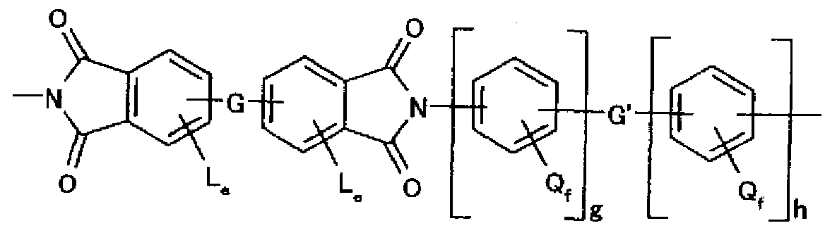


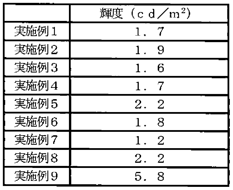
Claims
Priority Applications (1)
| Application Number | Priority Date | Filing Date | Title |
|---|---|---|---|
| US11/909,392 US20090068472A1 (en) | 2005-03-23 | 2006-01-30 | Method of producing an optical film, and image display apparatus using the optical film obtained by the production method |
Applications Claiming Priority (4)
| Application Number | Priority Date | Filing Date | Title |
|---|---|---|---|
| JP2005083183 | 2005-03-23 | ||
| JP2005-083183 | 2005-03-23 | ||
| JP2005152310 | 2005-05-25 | ||
| JP2005-152310 | 2005-05-25 |
Publications (1)
| Publication Number | Publication Date |
|---|---|
| WO2006100830A1 true WO2006100830A1 (ja) | 2006-09-28 |
Family
ID=37023518
Family Applications (1)
| Application Number | Title | Priority Date | Filing Date |
|---|---|---|---|
| PCT/JP2006/301411 Ceased WO2006100830A1 (ja) | 2005-03-23 | 2006-01-30 | 光学フィルムの製造方法、およびそのような製造方法により得られる光学フィルムを用いた画像表示装置 |
Country Status (4)
| Country | Link |
|---|---|
| US (1) | US20090068472A1 (ja) |
| KR (1) | KR20070104622A (ja) |
| TW (1) | TW200641487A (ja) |
| WO (1) | WO2006100830A1 (ja) |
Cited By (11)
| Publication number | Priority date | Publication date | Assignee | Title |
|---|---|---|---|---|
| WO2020196306A1 (ja) | 2019-03-28 | 2020-10-01 | 東洋紡株式会社 | 反射防止用円偏光板およびそれを用いた画像表示装置 |
| WO2020241312A1 (ja) | 2019-05-30 | 2020-12-03 | 東洋紡株式会社 | 折りたたみ型ディスプレイ用偏光板 |
| WO2020241313A1 (ja) | 2019-05-30 | 2020-12-03 | 東洋紡株式会社 | 折りたたみ型ディスプレイ |
| US11899167B2 (en) | 2019-05-28 | 2024-02-13 | Toyobo Co., Ltd. | Polyester film, laminated film, and use thereof |
| US11926720B2 (en) | 2019-05-28 | 2024-03-12 | Toyobo Co., Ltd. | Polyester film and application therefor |
| US11934226B2 (en) | 2019-02-08 | 2024-03-19 | Toyobo Co., Ltd. | Foldable display and portable terminal device |
| US11939499B2 (en) | 2019-05-28 | 2024-03-26 | Toyobo Co., Ltd. | Multilayer film and use of same |
| US11997916B2 (en) | 2019-02-08 | 2024-05-28 | Toyobo Co., Ltd. | Polyester film and use thereof |
| US12319801B2 (en) | 2019-07-12 | 2025-06-03 | Toyobo Co., Ltd. | Hard coating film for foldable display, and application of said film |
| US12354504B2 (en) | 2019-05-28 | 2025-07-08 | Toyobo Co., Ltd. | Transparent conductive polyester film and use of same |
| US12351730B2 (en) | 2019-07-12 | 2025-07-08 | Toyobo Co., Ltd. | Hard coat film for foldable display and use thereof |
Families Citing this family (9)
| Publication number | Priority date | Publication date | Assignee | Title |
|---|---|---|---|---|
| JP4918530B2 (ja) * | 2008-07-30 | 2012-04-18 | 日東電工株式会社 | 光学フィルム積層体の製造方法 |
| JP2013235272A (ja) | 2012-05-10 | 2013-11-21 | Samsung Electronics Co Ltd | 多層型光学フィルム、その製造方法及び表示装置 |
| KR101542618B1 (ko) * | 2012-12-14 | 2015-08-06 | 제일모직주식회사 | 편광판 및 이를 포함하는 광학 표시 장치 |
| KR20140133732A (ko) | 2013-05-10 | 2014-11-20 | 삼성전자주식회사 | 다층형 광학 필름, 그 제조 방법 및 표시 장치 |
| KR101821732B1 (ko) | 2013-12-02 | 2018-01-25 | 삼성전자주식회사 | 광학 필름, 그 제조 방법 및 표시 장치 |
| TWI614657B (zh) * | 2016-12-16 | 2018-02-11 | 奇象光學有限公司 | 光學膜片以及使用者輸入系統 |
| KR102126051B1 (ko) * | 2017-10-23 | 2020-06-23 | 삼성에스디아이 주식회사 | 액정 위상차 필름, 이를 포함하는 발광표시장치용 편광판 및 이를 포함하는 발광표시장치 |
| JP6935154B2 (ja) * | 2019-08-21 | 2021-09-15 | 日東電工株式会社 | 放射線透過抑制フィルム、ならびに該放射線透過抑制フィルムを用いた放射線透過抑制フィルターおよび撮影装置 |
| CN114153076B (zh) * | 2021-12-02 | 2023-11-21 | 宁波维真显示科技股份有限公司 | 3d偏振膜的制备装置及方法 |
Citations (5)
| Publication number | Priority date | Publication date | Assignee | Title |
|---|---|---|---|---|
| JPH07253573A (ja) * | 1994-03-15 | 1995-10-03 | Matsushita Electric Ind Co Ltd | 液晶表示素子 |
| JP2000190385A (ja) * | 1998-12-28 | 2000-07-11 | Nippon Mitsubishi Oil Corp | 光学フィルムの製造法、光学フィルム及び液晶表示装置 |
| JP2003114325A (ja) * | 2001-10-03 | 2003-04-18 | Nitto Denko Corp | 積層1/4波長板、円偏光板及びこれを用いた液晶表示装置、ならびにその製造方法 |
| JP2004279566A (ja) * | 2003-03-13 | 2004-10-07 | Seiko Epson Corp | 液晶表示装置および電子機器 |
| JP2004309772A (ja) * | 2003-04-07 | 2004-11-04 | Nippon Oil Corp | 光学積層体の製造方法、当該積層体からなる楕円偏光板、円偏光板および液晶表示装置 |
Family Cites Families (5)
| Publication number | Priority date | Publication date | Assignee | Title |
|---|---|---|---|---|
| US6593982B2 (en) * | 1999-11-01 | 2003-07-15 | Samsung Electronics Co., Ltd. | Liquid crystal display with color filter having depressed portion for wide viewing angle |
| US7561240B2 (en) * | 1998-10-30 | 2009-07-14 | Samsung Electronics Co., Ltd. | Common electrode on substrate having non-depressed surface portion overlapping opening in pixel electrode on opposite substrate and depressed portion partially overlapping edge of the pixel electrode |
| KR100590744B1 (ko) * | 1998-10-30 | 2006-10-13 | 삼성전자주식회사 | 컬러 필터 기판 및 그 제조 방법, 상기 컬러 필터 기판을 포함하는 액정 표시 장치 |
| US7462381B2 (en) * | 2002-04-26 | 2008-12-09 | Nitto Denko Corporation | Method for producing birefringent film |
| JP2004264345A (ja) * | 2003-02-03 | 2004-09-24 | Nitto Denko Corp | 位相差フィルムおよびその製造方法 |
-
2006
- 2006-01-30 US US11/909,392 patent/US20090068472A1/en not_active Abandoned
- 2006-01-30 KR KR1020077019206A patent/KR20070104622A/ko not_active Ceased
- 2006-01-30 WO PCT/JP2006/301411 patent/WO2006100830A1/ja not_active Ceased
- 2006-02-20 TW TW095105597A patent/TW200641487A/zh unknown
Patent Citations (5)
| Publication number | Priority date | Publication date | Assignee | Title |
|---|---|---|---|---|
| JPH07253573A (ja) * | 1994-03-15 | 1995-10-03 | Matsushita Electric Ind Co Ltd | 液晶表示素子 |
| JP2000190385A (ja) * | 1998-12-28 | 2000-07-11 | Nippon Mitsubishi Oil Corp | 光学フィルムの製造法、光学フィルム及び液晶表示装置 |
| JP2003114325A (ja) * | 2001-10-03 | 2003-04-18 | Nitto Denko Corp | 積層1/4波長板、円偏光板及びこれを用いた液晶表示装置、ならびにその製造方法 |
| JP2004279566A (ja) * | 2003-03-13 | 2004-10-07 | Seiko Epson Corp | 液晶表示装置および電子機器 |
| JP2004309772A (ja) * | 2003-04-07 | 2004-11-04 | Nippon Oil Corp | 光学積層体の製造方法、当該積層体からなる楕円偏光板、円偏光板および液晶表示装置 |
Cited By (13)
| Publication number | Priority date | Publication date | Assignee | Title |
|---|---|---|---|---|
| US11934226B2 (en) | 2019-02-08 | 2024-03-19 | Toyobo Co., Ltd. | Foldable display and portable terminal device |
| US11997916B2 (en) | 2019-02-08 | 2024-05-28 | Toyobo Co., Ltd. | Polyester film and use thereof |
| WO2020196306A1 (ja) | 2019-03-28 | 2020-10-01 | 東洋紡株式会社 | 反射防止用円偏光板およびそれを用いた画像表示装置 |
| US11939499B2 (en) | 2019-05-28 | 2024-03-26 | Toyobo Co., Ltd. | Multilayer film and use of same |
| US11926720B2 (en) | 2019-05-28 | 2024-03-12 | Toyobo Co., Ltd. | Polyester film and application therefor |
| US11899167B2 (en) | 2019-05-28 | 2024-02-13 | Toyobo Co., Ltd. | Polyester film, laminated film, and use thereof |
| US12354504B2 (en) | 2019-05-28 | 2025-07-08 | Toyobo Co., Ltd. | Transparent conductive polyester film and use of same |
| WO2020241313A1 (ja) | 2019-05-30 | 2020-12-03 | 東洋紡株式会社 | 折りたたみ型ディスプレイ |
| WO2020241312A1 (ja) | 2019-05-30 | 2020-12-03 | 東洋紡株式会社 | 折りたたみ型ディスプレイ用偏光板 |
| US12298547B2 (en) | 2019-05-30 | 2025-05-13 | Toyobo Co., Ltd. | Foldable display |
| US12548477B2 (en) | 2019-05-30 | 2026-02-10 | Toyobo Co., Ltd. | Polarization plate for folding display |
| US12319801B2 (en) | 2019-07-12 | 2025-06-03 | Toyobo Co., Ltd. | Hard coating film for foldable display, and application of said film |
| US12351730B2 (en) | 2019-07-12 | 2025-07-08 | Toyobo Co., Ltd. | Hard coat film for foldable display and use thereof |
Also Published As
| Publication number | Publication date |
|---|---|
| KR20070104622A (ko) | 2007-10-26 |
| TW200641487A (en) | 2006-12-01 |
| US20090068472A1 (en) | 2009-03-12 |
Similar Documents
| Publication | Publication Date | Title |
|---|---|---|
| JP3974631B2 (ja) | 光学フィルムおよびその製造方法、ならびに該光学フィルムを用いた画像表示装置 | |
| KR100618368B1 (ko) | 광학 필름 및 그 제조방법 | |
| WO2006100830A1 (ja) | 光学フィルムの製造方法、およびそのような製造方法により得られる光学フィルムを用いた画像表示装置 | |
| JP3701022B2 (ja) | 複屈折性光学フィルムの製造方法、前記製造方法により得られたフィルム、それを用いた楕円偏光板およびそれらを用いた液晶表示装置 | |
| JP4236101B2 (ja) | Vaモード液晶表示装置用視角補償フィルムの製造方法 | |
| JP4794012B2 (ja) | Va型液晶表示装置用重畳フィルムの製造方法、va型液晶表示装置用重畳フィルム及びva型液晶表示装置 | |
| JP4530256B2 (ja) | 位相差フィルム、その製造方法、およびこれを用いた光学フィルム | |
| JP4388023B2 (ja) | 光学補償層付偏光板、光学補償層付偏光板を用いた液晶パネル、液晶表示装置、および画像表示装置 | |
| JP4888931B2 (ja) | 液晶表示装置用重畳フィルムの製造方法、液晶表示装置用重畳フィルム及び液晶表示装置 | |
| WO2006064621A1 (ja) | 楕円偏光板およびその製造方法、ならびに楕円偏光板を用いた画像表示装置 | |
| JP2004046097A (ja) | 積層位相差板、それを用いた積層偏光板、ならびに画像表示装置 | |
| JP2007156234A (ja) | 光学フィルムの製造方法、光学フィルム、および光学フィルムを用いた画像表示装置 | |
| JP3929046B2 (ja) | 複屈折性フィルムの製造方法、複屈折フィルム、それを用いた光学補償層付き偏光板、垂直配向モード液晶表示装置用液晶パネル、および垂直配向モード液晶表示装置 | |
| JP4553258B2 (ja) | 楕円偏光板の製造方法および楕円偏光板を用いた画像表示装置 | |
| WO2006090520A1 (ja) | 楕円偏光板の製造方法および楕円偏光板を用いた画像表示装置 | |
| JP2004046068A (ja) | 複屈折層の製造方法、および前記複屈折層を含む光学フィルム | |
| JP3746050B2 (ja) | 光学補償フィルム、それを用いた光学補償層付偏光板、および、それらを用いた液晶表示装置 | |
| JP4274842B2 (ja) | Vaモードの液晶表示装置用の光学補償機能付き偏光板、及びそれを用いたvaモードの液晶表示装置 | |
| CN101133347A (zh) | 光学薄膜的制造方法、和使用由这样的制造方法制得的光学薄膜的图像显示装置 | |
| JP2008171007A (ja) | 複屈折フィルムの製造方法 | |
| JP2007148097A (ja) | 光学フィルムの製造方法、光学フィルム、および光学フィルムを用いた画像表示装置 | |
| JP2006259038A (ja) | 楕円偏光板の製造方法および楕円偏光板を用いた画像表示装置 | |
| JP2005258459A (ja) | 光学フィルムの製造方法 | |
| WO2007023673A1 (ja) | 液晶パネルおよびそれを用いた液晶表示装置 | |
| JP2006195478A (ja) | 光学フィルムの製造方法 |
Legal Events
| Date | Code | Title | Description |
|---|---|---|---|
| 121 | Ep: the epo has been informed by wipo that ep was designated in this application | ||
| WWE | Wipo information: entry into national phase |
Ref document number: 1020077019206 Country of ref document: KR |
|
| WWE | Wipo information: entry into national phase |
Ref document number: 200680006472.1 Country of ref document: CN |
|
| WWE | Wipo information: entry into national phase |
Ref document number: 11909392 Country of ref document: US |
|
| NENP | Non-entry into the national phase |
Ref country code: DE |
|
| NENP | Non-entry into the national phase |
Ref country code: RU |
|
| WWW | Wipo information: withdrawn in national office |
Ref document number: RU |
|
| 122 | Ep: pct application non-entry in european phase |
Ref document number: 06712554 Country of ref document: EP Kind code of ref document: A1 |
|
| WWW | Wipo information: withdrawn in national office |
Ref document number: 6712554 Country of ref document: EP |
|
| NENP | Non-entry into the national phase |
Ref country code: JP |