WO2005107332A1 - Organic light-emitting devices - Google Patents
Organic light-emitting devices Download PDFInfo
- Publication number
- WO2005107332A1 WO2005107332A1 PCT/CN2005/000522 CN2005000522W WO2005107332A1 WO 2005107332 A1 WO2005107332 A1 WO 2005107332A1 CN 2005000522 W CN2005000522 W CN 2005000522W WO 2005107332 A1 WO2005107332 A1 WO 2005107332A1
- Authority
- WO
- WIPO (PCT)
- Prior art keywords
- dopant
- organic light
- emitting device
- emissive layer
- group
- Prior art date
- Legal status (The legal status is an assumption and is not a legal conclusion. Google has not performed a legal analysis and makes no representation as to the accuracy of the status listed.)
- Ceased
Links
- 0 CC**(*(*)=*(*)*12)=C1C(O)=*(*1*)*2(*2*(*)=*3*)*1=C(**)C2=*3N Chemical compound CC**(*(*)=*(*)*12)=C1C(O)=*(*1*)*2(*2*(*)=*3*)*1=C(**)C2=*3N 0.000 description 1
Classifications
-
- H—ELECTRICITY
- H05—ELECTRIC TECHNIQUES NOT OTHERWISE PROVIDED FOR
- H05B—ELECTRIC HEATING; ELECTRIC LIGHT SOURCES NOT OTHERWISE PROVIDED FOR; CIRCUIT ARRANGEMENTS FOR ELECTRIC LIGHT SOURCES, IN GENERAL
- H05B33/00—Electroluminescent light sources
- H05B33/12—Light sources with substantially two-dimensional [2D] radiating surfaces
- H05B33/14—Light sources with substantially two-dimensional [2D] radiating surfaces characterised by the chemical or physical composition or the arrangement of the electroluminescent material, or by the simultaneous addition of the electroluminescent material in or onto the light source
-
- C—CHEMISTRY; METALLURGY
- C09—DYES; PAINTS; POLISHES; NATURAL RESINS; ADHESIVES; COMPOSITIONS NOT OTHERWISE PROVIDED FOR; APPLICATIONS OF MATERIALS NOT OTHERWISE PROVIDED FOR
- C09K—MATERIALS FOR MISCELLANEOUS APPLICATIONS, NOT PROVIDED FOR ELSEWHERE
- C09K11/00—Luminescent materials, e.g. electroluminescent or chemiluminescent
- C09K11/06—Luminescent materials, e.g. electroluminescent or chemiluminescent containing organic luminescent materials
-
- H—ELECTRICITY
- H10—SEMICONDUCTOR DEVICES; ELECTRIC SOLID-STATE DEVICES NOT OTHERWISE PROVIDED FOR
- H10K—ORGANIC ELECTRIC SOLID-STATE DEVICES
- H10K71/00—Manufacture or treatment specially adapted for the organic devices covered by this subclass
- H10K71/30—Doping active layers, e.g. electron transporting layers
-
- H—ELECTRICITY
- H10—SEMICONDUCTOR DEVICES; ELECTRIC SOLID-STATE DEVICES NOT OTHERWISE PROVIDED FOR
- H10K—ORGANIC ELECTRIC SOLID-STATE DEVICES
- H10K85/00—Organic materials used in the body or electrodes of devices covered by this subclass
- H10K85/30—Coordination compounds
- H10K85/341—Transition metal complexes, e.g. Ru(II)polypyridine complexes
- H10K85/346—Transition metal complexes, e.g. Ru(II)polypyridine complexes comprising platinum
-
- C—CHEMISTRY; METALLURGY
- C09—DYES; PAINTS; POLISHES; NATURAL RESINS; ADHESIVES; COMPOSITIONS NOT OTHERWISE PROVIDED FOR; APPLICATIONS OF MATERIALS NOT OTHERWISE PROVIDED FOR
- C09K—MATERIALS FOR MISCELLANEOUS APPLICATIONS, NOT PROVIDED FOR ELSEWHERE
- C09K2211/00—Chemical nature of organic luminescent or tenebrescent compounds
- C09K2211/10—Non-macromolecular compounds
- C09K2211/1003—Carbocyclic compounds
- C09K2211/1007—Non-condensed systems
-
- C—CHEMISTRY; METALLURGY
- C09—DYES; PAINTS; POLISHES; NATURAL RESINS; ADHESIVES; COMPOSITIONS NOT OTHERWISE PROVIDED FOR; APPLICATIONS OF MATERIALS NOT OTHERWISE PROVIDED FOR
- C09K—MATERIALS FOR MISCELLANEOUS APPLICATIONS, NOT PROVIDED FOR ELSEWHERE
- C09K2211/00—Chemical nature of organic luminescent or tenebrescent compounds
- C09K2211/10—Non-macromolecular compounds
- C09K2211/1003—Carbocyclic compounds
- C09K2211/1011—Condensed systems
-
- C—CHEMISTRY; METALLURGY
- C09—DYES; PAINTS; POLISHES; NATURAL RESINS; ADHESIVES; COMPOSITIONS NOT OTHERWISE PROVIDED FOR; APPLICATIONS OF MATERIALS NOT OTHERWISE PROVIDED FOR
- C09K—MATERIALS FOR MISCELLANEOUS APPLICATIONS, NOT PROVIDED FOR ELSEWHERE
- C09K2211/00—Chemical nature of organic luminescent or tenebrescent compounds
- C09K2211/10—Non-macromolecular compounds
- C09K2211/1018—Heterocyclic compounds
- C09K2211/1025—Heterocyclic compounds characterised by ligands
- C09K2211/1044—Heterocyclic compounds characterised by ligands containing two nitrogen atoms as heteroatoms
-
- C—CHEMISTRY; METALLURGY
- C09—DYES; PAINTS; POLISHES; NATURAL RESINS; ADHESIVES; COMPOSITIONS NOT OTHERWISE PROVIDED FOR; APPLICATIONS OF MATERIALS NOT OTHERWISE PROVIDED FOR
- C09K—MATERIALS FOR MISCELLANEOUS APPLICATIONS, NOT PROVIDED FOR ELSEWHERE
- C09K2211/00—Chemical nature of organic luminescent or tenebrescent compounds
- C09K2211/10—Non-macromolecular compounds
- C09K2211/1018—Heterocyclic compounds
- C09K2211/1025—Heterocyclic compounds characterised by ligands
- C09K2211/1059—Heterocyclic compounds characterised by ligands containing three nitrogen atoms as heteroatoms
-
- C—CHEMISTRY; METALLURGY
- C09—DYES; PAINTS; POLISHES; NATURAL RESINS; ADHESIVES; COMPOSITIONS NOT OTHERWISE PROVIDED FOR; APPLICATIONS OF MATERIALS NOT OTHERWISE PROVIDED FOR
- C09K—MATERIALS FOR MISCELLANEOUS APPLICATIONS, NOT PROVIDED FOR ELSEWHERE
- C09K2211/00—Chemical nature of organic luminescent or tenebrescent compounds
- C09K2211/18—Metal complexes
- C09K2211/185—Metal complexes of the platinum group, i.e. Os, Ir, Pt, Ru, Rh or Pd
-
- H—ELECTRICITY
- H10—SEMICONDUCTOR DEVICES; ELECTRIC SOLID-STATE DEVICES NOT OTHERWISE PROVIDED FOR
- H10K—ORGANIC ELECTRIC SOLID-STATE DEVICES
- H10K2101/00—Properties of the organic materials covered by group H10K85/00
- H10K2101/10—Triplet emission
-
- H—ELECTRICITY
- H10—SEMICONDUCTOR DEVICES; ELECTRIC SOLID-STATE DEVICES NOT OTHERWISE PROVIDED FOR
- H10K—ORGANIC ELECTRIC SOLID-STATE DEVICES
- H10K50/00—Organic light-emitting devices
- H10K50/10—OLEDs or polymer light-emitting diodes [PLED]
- H10K50/11—OLEDs or polymer light-emitting diodes [PLED] characterised by the electroluminescent [EL] layers
-
- Y—GENERAL TAGGING OF NEW TECHNOLOGICAL DEVELOPMENTS; GENERAL TAGGING OF CROSS-SECTIONAL TECHNOLOGIES SPANNING OVER SEVERAL SECTIONS OF THE IPC; TECHNICAL SUBJECTS COVERED BY FORMER USPC CROSS-REFERENCE ART COLLECTIONS [XRACs] AND DIGESTS
- Y10—TECHNICAL SUBJECTS COVERED BY FORMER USPC
- Y10S—TECHNICAL SUBJECTS COVERED BY FORMER USPC CROSS-REFERENCE ART COLLECTIONS [XRACs] AND DIGESTS
- Y10S428/00—Stock material or miscellaneous articles
- Y10S428/917—Electroluminescent
Definitions
- the present invention relates to efficient organic light-emitting devices (OLEDs) which comprise a transition metal complex, wherein the transition metal complex, of either geometrical isomers, comprises two bidentate NN-type ligands, or two bidentate NO-type ligands, or a tetradentate NNNN-type ligand, or a tetradentate NOON-type ligand, and a transition metal atom as the electrophosphorescent emitter.
- the invention also relates to methods for preparing thin film OLEDs and their applications such as in liquid crystal displays, plasma panel displays and light- emitting diodes.
- OLEDs Organic light-emitting devices
- FPDs flat-panel displays
- LCDs liquid crystal displays
- PDPs plasma display panels
- organometallic compounds exhibiting electroluminescence are particularly attractive for electrophosphorescent applications, since both the ligand structure and the central metal atom can be varied to modify the properties of the device using these compounds.
- An organic light-emitting device (OLED) is an energy conversion device which emits light when current is applied.
- a multilayer OLED is generally comprised of hole and electron injection layers, hole- and electron-transporting layers, an emissive layer, metal oxide layer and metal electrodes.
- organic small molecules and polymers in the emissive layer has attracted much attention due to their potential applications in full-color large-area flat-panel displays.
- Tang and NanSlyke first disclosed that organic small molecules can be prepared as thin-films by vacuum deposition to form multilayer organic light-emitting devices (OLEDs) (see Tang et al, Appl. Phys. Lett. 51:913, (1987)). Investigations on organic small molecules have been made in order to improve the performance of OLEDs.
- fluorescent and phosphorescent materials are employed as light emitters in the emissive layer of OLEDs. Light emission from a fluorescent compound occurs as a result of formation of singlet excitons in the emissive layer of the electroluminescent device.
- Patent No. 6,310,360 disclosed that theoretically 25 % singlet excitons and 75 % triplet excitons are produced after recombination of holes and electrons in the emissive layer of an electroluminescent device.
- the singlet excitons transfer their energy to the singlet excited state while the triplet excitons transfer their energy to triplet excited state.
- Most of the organic small molecules exhibit fluorescence; hence, only 25 % of the generated excitons are utilized resulting in the device with low external efficiency.
- fluorescent compounds a series of effective phosphorescent iridium complexes with different color emissions has been reported jointly by Thompson et al. at the University of Southern California and Forrest et al. at Princeton University (see U.S. Patent No.
- H2OEP octylethylporphyrin
- Thompson and Forrest et al. reported a red phosphorescent material (bis(2-(2'-benzo[4,5- a]thienyl)pyridinato-N, C 3 ) iridium (acetylacetonate) [Btp2Ir(acac)]) with high-
- the main objective of this invention is to provide organic hght-emitting devices (OLEDs) comprising an emissive layer, which employs at least one dopant complex as an electrophosphorescent emitter.
- OLEDs organic hght-emitting devices
- the devices should exhibit low turn-on voltages, high luminance, high efficiencies, and desirable colors.
- Another objective of the present invention is to provide an OLED structure, which employs an emissive layer comprising at least one electrophosphorescent dopant complex and at least one host material.
- Yet another objective is to provide OLEDs that emit desirable colors by varying concentration of the dopant complex in the emissive layer under different applied voltages. It is concerned with the efficiencies of the selected dopant complexes, which can be used at low concentration levels in OLEDs.
- the invention relates to a heterostructured organic light- emitting device comprising: a substrate upon which a first electrode is placed; a hole-transporting layer; at least one emissive layer comprising at least one host material and at least one dopant complex; the dopant complex, of either geometrical isomers, comprising at least one transition metal coordinated to two bidentate NN-type ligands, or two bidentate NO-type ligands, or a tetradentate NNNN-type hgand, or a tetradentate NOON-type hgand; a hole-blocking layer; an electron-transporting layer; a charge injection layer; and a second electrode sandwiching the hole-transporting layer, emissive layer, hole-blocking layer, electron-transporting layer and charge injection layer between the first and the second electrode.
- the invention relates to OLED comprising an emissive layer which contains at least one transition metal complex.
- the transition metal complexes contain two bidentate NN-type hgand, or two bidentate NO-type ligands, or a tetradentate NNNN-type hgand, or a tetradentate NOON-type hgand, and a transition metal as the electrophosphorescent dopant complexes.
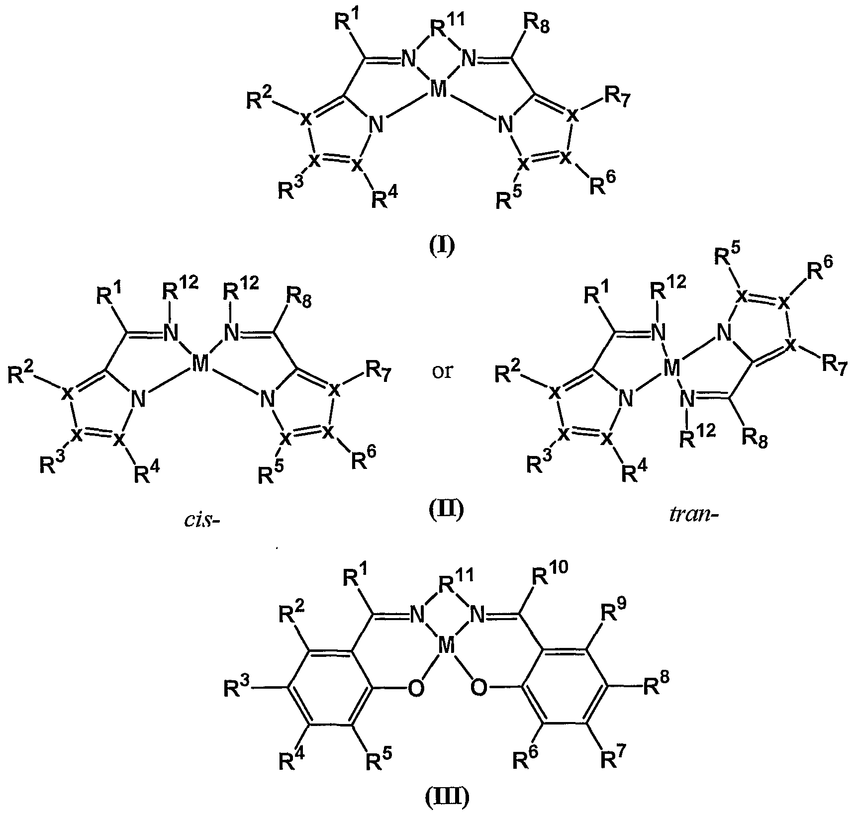
- the invention relates to a heterostructured OLED comprising one or more dopant complexes of following formulae:
- CIS- (IV) tran- or mixtures thereof wherein M is a transition metal selected from the group consisting of Ni, Pd and Pt; each R ⁇ R 10 is independently -H, -OH, -NH 2 , -halogen, -CN, -NO 2 , -R 13 , -OR 14 , NHR 14 , or -N(R 14 ) 2 ; R 11 is -(C(R 15 )2)n,
- each R 12 is independently -H, -(C ⁇ -C6)alkyl, -phenyl, -naphthyl; -halogen, or -CN;
- R 13 is -(C r C 6 )alkyl, -phenyl, or -naphthyl, each of which is unsubstituted or substituted with one or more -phenyl, or -naphthyl;
- R 14 is defined as above for R 13 ; and R 15 is defined as above for R 1 ;
- x is independently a carbon or nitrogen atom; and n is an integer number from 1 to 6.
- the present invention relates to a method of preparing heterostructured organic light emitting devices with yellow, orange or red color emissions.
- the method includes the steps of: providing a substrate upon which a first electrode is placed; providing a hole-transporting layer on top of the first electrode; forming an emissive layer on top of the hole-transporting layer, the emissive layer comprising at least one host material and at least one dopant complex, the dopant complex, of either geometrical isomers, comprising a transition metal coordinated to two bidentate NN-type ligands, or two bidentate NO-type hgands, or a tetradentate NNNN-type ligand, or a tetradentate NOON-type ligand.
- OLEDs comprising hetero structures for producing red, orange or yellow electroluminescence; the devices contain an anode (ITO glass substance), a hole- transporting layer (N,N-diphenyl-N,N-bis(2-naphthalene)benzidine (E- ⁇ PB)), an
- emissive layer comprising a host material (4,4'-bis(carbazol-9-yl)biphenyl (CBP)) and an electrophosphorescent dopant complex as illustrated in Formulae I, H, HI or IV herein), a hole-blocking layer (2,9-dimethyl-4,7-diphenyl-l,10-phenanthroline (BCP)), an electron-transporting layer (tris(8-hydroxyquinolato) aluminum (Alq 3 )), a charge injection layer (hthium fluoride) and a cathode (aluminum metal).
- CBP 4,4'-bis(carbazol-9-yl)biphenyl
- BCP hole-blocking layer
- an electron-transporting layer tris(8-hydroxyquinolato) aluminum (Alq 3 )
- charge injection layer hthium fluoride
- cathode aluminum metal
- the OLEDs employing electrophosphorescent dopant complexes as illustrated in Formulae I, H, IH or IV herein demonstrate red, orange or yellow emission while a current is applied.
- the high efficiency OLEDs can be applied to the field of electronic flat panel display, display board for sign lamp or light source.
- FIG. 1 Absorption, excitation and emission spectra of dopant complex 1 in CH 3 CN FIG. 2.
- Schematic diagram of OLED in present invention FIG 5. EL spectra of OLED A with 4.0 wt.% dopant 1 at different dopant concentrations under 8 V FIG 6.
- FIG. 25 EL spectra of OLED F with 1.6 wt.% dopant 107 at different dopant concentrations at 8 V
- FIG. 26 EL spectra of OLED F with 1.6 wt.% dopant 107 at different apphed voltages
- FIG. 27 V-I-B curve of OLED F with 1.6 wt.% dopant 104
- FIG. 28 External quantum efficiency and luminous efficiency of OLED F with
- the phrase “bidentate NN-type hgands” refers to a molecule containing an imine group and either a pyrrol group, a pyrazol group, an imidazol group, or a triazol group, which ligand is coordinated to a metal through the nitrogen atoms of these groups.
- the phrase “bidentate NO-type hgands” refers to a molecule containing an imine group and a phenoxide group, which ligand is coordinated to a metal through the nitrogen and oxygen atoms of these groups.
- the phrase "tetradentate NNNN-type hgand” refers to a molecule containing a two imine groups and either two pyrrol groups, two pyrazol groups, two imidazol groups, or two triazol groups, which ligand is coordinated to a metal through the nitrogen atoms of these groups.
- the phrase “tetradentate NOON-type hgand” refers to a molecule containing two imine groups and two phenoxide groups, which hgand is coordinated to a metal through the nitrogen and oxygen atoms of these groups.
- the phrase “light-emitting device” refers to structures presenting an assymetric impedance to current.
- the present invention is related to a heterostructured OLED comprising an emissive layer, wherein the emissive layer comprises at least one host material and at least one emissive material.
- the emissive material is a dopant complex, of either geometrical isomers, comprising a transition metal coordinated to two bidentate NN-type ligands, or two bidentate NO-type hgands, or a tetradentate NNNN-type ligand, or a tetradentate NOON-type ligand.
- the dopant complex can be present as a monomer, a dimer, an ohgomer, or mixtures thereof.
- the invention relates to a heterostructured organic light- emitting device comprising: a substrate upon which a first electrode is placed; a hole-transporting layer; at least one an emissive layer comprising at least one host material and at least one dopant complex; the dopant complex, of either geometrical isomers, comprising at least one transition metal coordinated to two bidentate NN- type ligands or two bidentate NO-type hgands or a tetradentate NNNN-type ligand or a tetradentate NOON-type hgand; a hole-blocking layer; an electron-transporting layer; a charge injection layer; and a second electrode sandwiching the hole-transporting layer, emissive layer, hole-blocking layer, electron-transporting layer and charge injection layer between the first and the second electrode.
- the emissive materials are dopant complexes, of either geometrical isomers, comprising two bidentate NN-type ligands or two bidentate NO-type hgands or a tetradentate NNNN-type hgand or a tetradentate NOON-type hgand and a transition metal atom. More preferably, the emissive materials include dopant complexes of the following formulae:
- CIS- (IV) tran- or mixtures thereof wherein M is a transition metal selected from the group consisting of Ni, Pd and Pt; each R ⁇ R 10 is independently -H, -OH, -NH 2 , -halogen, -CN, -NO* -R 13 , -OR 14 , NHR 14 , or -N(R 14 ) 2 ; R ⁇ is -(C(R 15 »n-,
- each R 12 is independently -H, -(C ⁇ -C6)alkyl, -phenyl, -naphthyl; -halogen, or -CN;
- R 13 is -(C r C 6 )alkyl, -phenyl, or -naphthyl, each of which is unsubstituted or substituted with one or more -(C r C 6 )alkyl, -phenyl, or -naphthyl;
- R 14 is defined as above for R 13 ; and
- R 15 is defined as above for R 1 ;
- x is independently carbon or nitrogen atom; and
- n is an integer from 1 to 6.
- the compounds of formulae (I), (H), (HI) or (IV) may comprise R ⁇ R 10 groups that are electron donors.
- Non-hmiting examples of electron donor groups are amines including -N(R 14 ) 2 and -OR 14 .
- the compounds of formulae (I), (H), (HI) or (IV) may comprise R ⁇ R 10 groups that are electron acceptors.
- Non-limiting examples of electron acceptor groups include -F, -Cl, -Br, -I, -NO 2 , -C(O)(C r C 6 ), -C(O)O(C r C 6 ), -SCN, -SO 3 F and -CN.
- Non-limiting examples of bidentate NN-type hgands include those shown above for dopant complexes 3 and 14 to 18.
- NN-type hgands are selected from hgands consisting of at least an unsubstituted 5-membered or 6- membered ring or substituted 5-membered or 6-membered ring; wherein the substituted 5-membered or 6-membered ring includes at least one substituent selected from the groups; a hydrogen, a halogen, a hydroxyl group, an alkyl group, a cycloalkyl group, an aryl group, an acyl group, an alkoxy, an acyloxy group, an amino group, an acyl amino group, an aralkyl group, a cyano group, a carboxyl group, a thio group, a vinyl group, a styryl group, an aminocarbonyl group, a carbonyl group, an aranyl group, an aryloxycarbon
- the transition metal is Pt.
- bidentate NO-type hgands include those shown above for dopant complexes 67 to 98.
- NO-type hgands are selected from ligands consisting of at least an un-substituted 6-membered or 5-membered ring or substituted 6-membered or 5-membered ring; wherein the substituted 6-membered or 5-membered ring includes at least one substituent selected from the groups; a hydrogen, a halogen, a hydroxyl group, an alkyl group, a cycloalkyl group, an aryl group, an acyl group, an alkoxy, an acyloxy group, an amino group, an acyl amino group, an aralkyl group, a cyano group, a carboxyl group, a thio group, a vinyl group, a styryl group, an aminocarbonyl group, a carbonyl group,
- NNNN-type hgands include those shown above for dopant complexes 1-2 and 4-13.
- NNNN-type hgands are selected from ligands consisting of at least an unsubstituted 5-membered or 6-membered ring or substituted 5-membered or 6-membered ring; wherein those substituted 5-membered or 6-membered ring includes at least a substituent selected from the groups; a hydrogen, a halogen, a hydroxyl group, an alkyl group, a cycloalkyl group, an aryl group, an acyl group, an alkoxy, an acyloxy group, an amino group, an acyl amino group, an aralkyl group, a cyano group, a carboxyl group, a thio group, a vinyl group, a styryl group, an aminocarbonyl group, a carbonyl group,
- NOON-type ligands include those shown above for dopant complexes 19-66 and 99-178.
- NOON-type hgands are selected from hgands consisting of at least an unsubstituted 6-membered or 5-membered ring or substituted 6-membered or 5-membered ring; wherein those substituted 6- membered or 5-membered ring includes at least a substituent selected from the groups; a hydrogen, a halogen, a hydroxyl group, an alkyl group, a cycloalkyl group, an aryl group, an acyl group, an alkoxy, an acyloxy group, an amino group, an acyl amino group, an aralkyl group, a cyano group, a carboxyl group, a thio group, a vinyl group, a styryl group, an aminocarbonyl group, a carbonyl group,
- the transition metal is Pt.
- the present invention is also directed to methods for preparation of OLEDs that can be fabricated by a vapor deposition process.
- OLEDs contain an anode, a hole-transporting layer, an emissive layer comprising at least one host material and at least one dopant complex, a hole-blocking layer, an electron-transporting layer, a charge injection layer and a cathode.
- an anode useful for OLEDs are indium-tin-oxide (ITO) and doped polyaniline.
- Non-limiting examples of hole-transporting materials useful in the present invention are beryllium bis(2-(2'-hydroxyphenyl)pyridine, 4,4'-bis(carbazol-9-
- host materials useful in the present invention include beryllium bis(2-(2'-hydroxyphenyl)pyridine, 4,4'-bis(carbazol-9-yl)biphenyl (CBP), N,N-diphenyl-N,N , -bis(l-na ⁇ hthalene)benzidine ( ⁇ - ⁇ PB), N,7Y-diphenyl- N,N-bis(2-naphthalene)benzidine O ⁇ PB), N,N-bis(3 -methylphenyl)-N,N- bis(phenyl)benzidine (TPD), 4,4',4"-tris(N-3-methyl ⁇ henyl-N- phenylamino)triphenylamine (m-TD ATA) tetrakis(diarylamino)-9, 9'-spirobifluorenes, beryllium bis(2-(2'-hydroxyphenyl)pyridine (Bepp 2 ), 3-phenyl-4-(l'-n
- At least one suitable host material was employed in an emissive layer together with at least one dopant complex.
- dopant complexes of either geometrical isomers, comprising a transition metal coordinated to two bidentate ⁇ -type ligands, or two bidentate ⁇ O-type hgands, or a tetradentate ⁇ -type hgand, or a tetradentate ⁇ OO ⁇ -type hgand include those shown for dopant complexes 1-178 in Table 1 and 2 above.
- the dopant complexes are selected from the groups consisting of dopant complexes 1-18, 19, 22, 24-25, 27, 30, 32-33, 35, 38, 40-41, 43, 46, 48-49, 51, 54, 56-57, 59, 62, 64-65, 99, 102, 104-105, 107, 110, 112-113, 115, 118, 120-121, 123, 126, 128-129 and mixtures thereof. More preferably, the dopant complexs are 1, 2, 4, 19, 35, 51, 99 and 104.
- hole-blocking layer suitable for the present invention include 3,4,5-triphenyl-l,2,4-triazole, 3-(biphenyl-4-yl)-4-phenyl-5-(4-tert- butylphenyl)- 1 ,2,4-triazole (TAZ), 2,9-dimethyl-4.7-diphenyl- 1 , 10-phenanthrohne (BCP) and 1 ,3.5-tris[5-(4-(l , 1 -dimethylethyl) ⁇ henyl)- 1 ,3 ,4-oxadiazol-2-yl]benzene (TBOP).
- 3,4,5-triphenyl-l,2,4-triazole 3-(biphenyl-4-yl)-4-phenyl-5-(4-tert- butylphenyl)- 1 ,2,4-triazole (TAZ), 2,9-dimethyl-4.7-diphenyl- 1 , 10-phenanthrohne (BCP) and 1 ,3.5
- Non-limiting examples of electron-transporting materials for the present invention include tris(8-hydroxyquinolato) aluminum (Alc ⁇ ) and 2-(4-biphenylyl)-5- (p-tert-butylphenyl)- 1 ,3 ,4-oxadiazole.
- Non-limiting examples of charge injection layer suitable for the present invention include hthium fluoride, cesium fluoride and lithium benzoate.
- Non-limiting examples of low work function metals for use as cathode in the present invention include aluminum, potassium, hthium, magnesium, silver, gold, rubidium, beryllium and cesium.
- the, OLED described herein comprises hetero structures for producing electroluminescence which contain an anode (ITO
- naphthalene)benzidine (/2- ⁇ PB)
- a matrix emissive layer including a host material
- OLEDs comprising dopant complexes as illustrated in Formula I, H, HI or IV herein exhibit red, orange or yellow electroluminescence.
- the concentration of the dopant complexes in the emissive layer can range from 0.5 to 8.0 wt.% based on the efficiency of energy conversion between dopant complexes and host materials and molecular structure of dopant complexes. However, other concentrations can be used.
- concentration of the dopant complexes in the emissive layer can range from 0.5 to 8.0 wt.% based on the efficiency of energy conversion between dopant complexes and host materials and molecular structure of dopant complexes. However, other concentrations can be used.
- the following examples are set forth to aid in understanding of the inventions but are not intended to, and should not be interpreted to, hmit in any way the claimed invention.
- Example 1 shows the synthesis of dopant complex 1.
- the tetradentate NNNN- type hgand was prepared according to modification of literature procedures (see Bacchi et al, InorganicaChimica Ada. 342:229, (2003); Male et al, J. Chem. Soc, Dalton Trans. 2487, (1997)).
- Example 2 shows the photophysical properties of non-limiting illustrative emissive materials corresponding to dopant complexes 1, 2 and 4 of the present invention.
- the absorption and photoluminescence properties of dopant complexes are provided in Table 3.
- UV/vis absorption, excitation and emission spectra of dopant complexes 1, 2 and 4 are shown in FIG. 1 to 3 respectively.
- the photoluminescence (PL) spectrum is substantially independent of excitation wavelength from 300 to 450 nm. At room temperature, strong PL emissions are obtained with quantum yields ( ⁇ ) up to 0.110 in CH 3 CN.
- the emission hfethnes of the dopant complexes range from 0.57 to 4.25 ⁇ s.
- FIG. 1 shows representative UV/vis absorption, excitation and emission spectra of dopant complex 1 in CH 3 CN solution.
- an orange photoluminescence PL
- FIG. 2 depicts the UV/vis, excitation and emission spectra of dopant complex
- FIG. 3 shows the UV/vis absorption, excitation and emission spectra of dopant complex 4 in CH 3 CN solution.
- Example 3 illustrates a non-limiting method for preparing an OLED of the present invention.
- the electroluminescent devices were prepared on patterned indium- tin-oxide (ITO) glass with a sheet resistance of 20 ⁇ / square.
- the glass was cleaned sequentially in detergent solution, deionized water, ethanol and acetone. After the wet-cleaning process, the ITO glass was dried at 130 °C for 1 h and treated in UV ozone cleaner for 10 mins.
- ITO indium- tin-oxide
- the device configuration is ITO/NPB (40 nm)/CBP:X wt.% dopant complex as illustrated in formulae (I), (II), (III) or (IV) (30 nm)/BCP (20 nm)/Alq 3 (30 nm)/LiF (0.5 nm)/Al (150 nm); all of the layers were grown sequentially by thermal deposition at a deposition rate of about 0.2 A sec or about 5 A /sec under a vacuum of 1 10 "6 Torr.
- the configuration of OLED in the present invention is schematically shown in FIG. 4. The device has multiple layers as shown.
- anode layer 410 preferably comprising indium-tin-oxide is deposited upon substrate layer 405.
- the substrate can be glass or other material through which the electroluminescence can traverse.
- Hole-transporting layer 415 comprising NPB is placed on top of layer 410.
- Emissive layer 420 employing CBP host and dopant complex is in contact with hole- transporting layer 415.
- a hole-blocking layer 425 containing BCP is deposited on the emissive layer 420.
- an electron-transporting layer 430 Adjacent to the hole-blocking layer 425, an electron-transporting layer 430, preferably Alq 3 , is placed on it.
- a charge injection layer 435 comprising LiF is then deposited on the layer 430.
- a cathode layer 440 is fabricated on top of the layer 435.
- the thickness for NPB is 40 nm (hole-transporting layer 415) and the emissive layer 420 is about 30 nm thick; the hole-blocking layer 425 is 20 nm and electron-transporting layer 430 is 30 nm.
- the charge transport layer 435 is 0.5 nm thick and cathode layer 440 is preferably about 150 nm thick.
- the emissive area of device is 3 X 3 mm 2 , which is defined by overlapping area between cathode and
- glass substrate 405 need not be flat in all embodiments of the invention.
- the glass substrate 405 is shaped, for instance, in a concave shape to focus the light generated in emissive layer 420, which provides even greater hght intensity in a small region.
- the glass substrate 405 is shaped, for instance, in a convex shape that spreads the generated hght more diffusely.
- EXAMPLE 4 Example 4 shows a red OLED A employing dopant complex 1 as dopant in a CBP host.
- the configuration of device A is ITO/NPB (40 nm)/CBP:4 wt.% dopant 1 (30 nm)/BCP (20 nm)/Alq 3 (30 nm)/LiF (0.5 nm)/Al (150 nm).
- CIE__1931 1931 Commission Internationale de L'Eclairage
- FIG. 5 shows EL spectra of the OLED A with 4.0 wt.% dopant 1 at different dopant concentrations under 8 V.
- FIG. 6 shows EL spectra of the OLED A with 4.0 wt.% dopant 1 at different applied voltage.
- FIG. 7 depicts V-I-B curve of the OLED A with 4.0 wt.% dopant 1.
- FIG. 8 shows external quantum efficiency and luminous efficiency of the OLED A with 4.0 wt.% dopant 1.
- Table 4 shows the EL performance of OLED A with 4.0 wt.% dopant 1 at different dopant concentrations.
- the device configuration is ITO/NPB (40 nm)/CBP:5 wt.% dopant 2 (30 nm)/BCP (20 nm)/Alq 3 (30 nm)/LiF (0.5 nm)/Al (150 nm).
- CIE_1931 1931 Commission Internationale de L'Eclairage
- FIG. 9 shows the EL spectra of OLED B with 5 wt.% dopant 2 at different dopant concentrations at 8 Y.
- FIG. 10 shows the EL spectra of OLEDs B with 5 wt.% dopant 2 at different apphed voltages.
- FIG. 11 shows the V-I-B curve of OLED B with 5 wt.% dopant 2.
- FIG. 12 shows the external quantum efficiency and luminous efficiency of OLED B with 5.0 wt.% dopant 2.
- Table 5 shows the EL performance of OLED B with dopant 2 at different dopant concentrations.
- the configuration of device C is ITO/NPB (40 nm)/CBP:3 wt.% dopant 19 (30 nm)/BCP (20 nm)/Alq 3 (30 nm)/LiF (0.5 nm)/Al (150 nm).
- CIE_1931 1931 Commission Internationale de L'Eclairage
- FIG. 13 shows the EL spectra of OLED C with 3 wt. % dopant 19 at different dopant concentrations at 8 V.
- FIG. 14 shows the EL spectra of OLED C with 3 wt.% dopant 19 at different apphed voltages.
- FIG. 15 shows the V-I-B curve of OLED C with 3 wt.% dopant 19.
- FIG. 16 shows the external quantum efficiency and luminous efficiency of OLED C with 3.0 wt.% dopant 19.
- Table 6 shows the EL performance of OLED C with dopant 19 at different dopant concentrations. Table 6.
- Example 7 shows a yellow OLED D employing dopant complex 51 as dopant in a CBP host.
- the configuration of device D is ITO/NPB (40 nm)/CBP:4 wt.% dopant 51 (30 nm)/BCP (20 nm)/Alq 3 (30 nm)/LiF (0.5 nm)/Al (150 nm).
- CBE_1931 1931 Commission Internationale de L'Eclairage
- FIG. 17 shows the EL spectra of OLED D with 4 wt.% dopant 51 at different dopant concentrations at 8 V.
- FIG. 18 shows the EL spectra of OLED D with 4 wt.% dopant 51 at different applied voltages.
- FIG. 19 shows the V-I-B curve of OLED D with 4 wt.% dopant 51,
- FIG. 20 shows the external quantum efficiency and luminous efficiency of OLED D with 4.0 wt.% dopant 51.
- Table 7 shows the EL performance of OLED D with dopant 51 at different dopant concentrations. Table 7.
- Example 8 shows a red OLED E employing dopant complex 99 as dopant in a CBP host.
- CIE_1931 1931 Commission Internationale de L'Eclairage
- FIG. 21 shows the EL spectra of OLED E with 1.5 wt.% dopant 99 at different dopant concentrations at 8 V.
- FIG. 22 shows the EL spectra of OLED E with 1.5 wt.% dopant 99 at different applied voltages.
- FIG. 23 shows the V-I-B curve of OLED E with 1.5 wt.% dopant 99.
- FIG. 24 shows the external quantum efficiency and luminous efficiency of OLED E with 1.5 wt.% dopant 99.
- Table 8 shows the EL performance of OLED E with dopant 99 at different dopant concentrations.
- Table 8. EL performance of OLED E with dopant 99 at different dopant concentrations
- Example 9 shows a red OLED F employing dopant complex 104 as dopant in a CBP host.
- the configuration of device F is ITO/NPB (40 nm)/CBP:1.6 wt.% dopant 104 (30 nm)/BCP (20 nm)/Alq 3 (30 nm)/LiF (0.5 nm)/Al (150 nm).
- CIE_1931 1931 Commission Internationale de L'Eclairage
- FIG. 25 shows the EL spectra of OLED F with 1.6 wt.% dopant 104 at different dopant concentrations at 8 V.
- FIG. 26 shows the EL spectra of OLED F with 1.6 wt.% dopant 104 at different apphed voltages.
- FIG. 27 shows the V-I-B curve of OLED F with 1.6 wt.% dopant 104.
- FIG. 28 shows the external quantum efficiency and luminous efficiency of OLED F with 1.6 wt.% dopant 104.
- Table 9 shows the EL performance of OLED F with dopant 104 at different dopant concentrations.
- Table 9. EL performance of OLED F with dopant 104 at different dopant concentrations
- an advantage of the OLEDs of the present invention is that the color of the emitted hght may be tuned during fabrication by changing the concentration of the dopant complex.
- the color and/or intensity of the emission of the OLEDs of the present invention may be changed by the use of filters, as is known in the art.
- filters as is known in the art.
Landscapes
- Chemical & Material Sciences (AREA)
- Engineering & Computer Science (AREA)
- Materials Engineering (AREA)
- Organic Chemistry (AREA)
- Crystallography & Structural Chemistry (AREA)
- Inorganic Chemistry (AREA)
- Manufacturing & Machinery (AREA)
- Electroluminescent Light Sources (AREA)
Abstract
Description


Claims


Priority Applications (2)
| Application Number | Priority Date | Filing Date | Title |
|---|---|---|---|
| DE112005000865T DE112005000865B4 (en) | 2004-04-30 | 2005-04-18 | Organic light-emitting components |
| JP2007509853A JP5149000B2 (en) | 2004-04-30 | 2005-04-18 | Organic light emitting device |
Applications Claiming Priority (2)
| Application Number | Priority Date | Filing Date | Title |
|---|---|---|---|
| US10/835,481 | 2004-04-30 | ||
| US10/835,481 US20050244672A1 (en) | 2004-04-30 | 2004-04-30 | Organic light-emitting devices |
Publications (1)
| Publication Number | Publication Date |
|---|---|
| WO2005107332A1 true WO2005107332A1 (en) | 2005-11-10 |
Family
ID=35187456
Family Applications (1)
| Application Number | Title | Priority Date | Filing Date |
|---|---|---|---|
| PCT/CN2005/000522 Ceased WO2005107332A1 (en) | 2004-04-30 | 2005-04-18 | Organic light-emitting devices |
Country Status (5)
| Country | Link |
|---|---|
| US (2) | US20050244672A1 (en) |
| JP (1) | JP5149000B2 (en) |
| CN (1) | CN100487943C (en) |
| DE (1) | DE112005000865B4 (en) |
| WO (1) | WO2005107332A1 (en) |
Cited By (3)
| Publication number | Priority date | Publication date | Assignee | Title |
|---|---|---|---|---|
| JP2011503886A (en) * | 2007-11-12 | 2011-01-27 | メルク パテント ゲーエムベーハー | Organic electroluminescent device |
| WO2020088582A1 (en) * | 2018-10-31 | 2020-05-07 | Versitech Limited | Platinum (ii) schiff base complexes with increased emission quantum yield for red oled applications |
| CN112358430A (en) * | 2020-11-02 | 2021-02-12 | 南方科技大学 | Schiff base metal complex and preparation method thereof, perovskite solar cell and preparation method thereof |
Families Citing this family (32)
| Publication number | Priority date | Publication date | Assignee | Title |
|---|---|---|---|---|
| JP5008974B2 (en) * | 2004-05-18 | 2012-08-22 | 日本放送協会 | Light emitting element |
| JP2006295104A (en) | 2004-07-23 | 2006-10-26 | Semiconductor Energy Lab Co Ltd | LIGHT EMITTING ELEMENT AND LIGHT EMITTING DEVICE USING THE SAME |
| JP4762527B2 (en) * | 2004-11-10 | 2011-08-31 | 富士フイルム株式会社 | Organic electroluminescence device |
| JP4311429B2 (en) * | 2006-09-27 | 2009-08-12 | セイコーエプソン株式会社 | Method for manufacturing organic electroluminescent device and organic electroluminescent device |
| DE102007037905B4 (en) * | 2007-08-10 | 2011-02-24 | Fraunhofer-Gesellschaft zur Förderung der angewandten Forschung e.V. | Doped semiconductor material and its use |
| JP5050813B2 (en) * | 2007-11-29 | 2012-10-17 | ソニー株式会社 | Memory cell |
| DE102008057050B4 (en) * | 2008-11-13 | 2021-06-02 | Merck Patent Gmbh | Materials for organic electroluminescent devices |
| DE102008057051B4 (en) * | 2008-11-13 | 2021-06-17 | Merck Patent Gmbh | Materials for organic electroluminescent devices |
| US20100314994A1 (en) | 2009-06-16 | 2010-12-16 | Chi Ming Che | Platinum (II) Isoqulinoline-Pyridine-Benzene Based Complexes, Methods for Making Same, and Organic Light-Emitting Diodes Including Such Complexes |
| JP2011046699A (en) * | 2009-07-31 | 2011-03-10 | Sumitomo Chemical Co Ltd | Metal complex, composition including the same, and light-emitting element using the same |
| US8877353B2 (en) | 2010-07-21 | 2014-11-04 | Versitech Limited | Platinum (II) tetradentate ONCN complexes for organic light-emitting diode applications |
| US8957217B2 (en) | 2011-05-31 | 2015-02-17 | The University Of Hong Kong | Phosphorescent material, their preparations and applications |
| EP2737553A1 (en) | 2011-07-25 | 2014-06-04 | Merck Patent GmbH | Copolymers with functionalized side chains |
| WO2013013753A2 (en) | 2011-07-25 | 2013-01-31 | Merck Patent Gmbh | Polymers and oligomers with functionalized side groups |
| DE102011079847A1 (en) | 2011-07-26 | 2013-01-31 | Eberhard-Karls-Universität Tübingen | Complexes with anionic ligands with two P donors and their use in the opto-electronic domain |
| DE102011079856A1 (en) | 2011-07-26 | 2013-01-31 | Eberhard-Karls-Universität Tübingen | Complex compounds with a ligand having an N- and a P-donor and their use in the opto-electronic domain |
| DE102011079857B4 (en) * | 2011-07-26 | 2013-03-21 | Eberhard-Karls-Universität Tübingen | Complexes with tetradentate ligands and their use in the opto-electronic domain |
| JP5967663B2 (en) * | 2011-09-08 | 2016-08-10 | 国立大学法人大阪大学 | Platinum complex |
| US9234274B2 (en) * | 2012-11-08 | 2016-01-12 | Applied Materials, Inc. | Method of atomic layer deposition of elemental metal |
| WO2015053291A1 (en) * | 2013-10-11 | 2015-04-16 | 国立大学法人大阪大学 | Light-emitting material including platinum complex |
| JP6319888B2 (en) * | 2014-03-11 | 2018-05-09 | 国立大学法人大阪大学 | Platinum complex and luminescent material containing the same |
| CN105273712B (en) * | 2014-07-11 | 2017-07-25 | 广东阿格蕾雅光电材料有限公司 | Luminescent materials for light-emitting diodes |
| KR102344885B1 (en) * | 2015-01-09 | 2021-12-29 | 삼성전자주식회사 | Organometallic compound and organic light-emitting device including the same |
| US10592742B1 (en) * | 2015-09-28 | 2020-03-17 | Amazon Technologies, Inc. | Agent re-identification |
| US11228002B2 (en) * | 2016-04-22 | 2022-01-18 | Universal Display Corporation | Organic electroluminescent materials and devices |
| US11228003B2 (en) * | 2016-04-22 | 2022-01-18 | Universal Display Corporation | Organic electroluminescent materials and devices |
| CN106478451A (en) * | 2016-09-18 | 2017-03-08 | 台州学院 | A kind of orange light luminescent material and preparation method thereof |
| CN106431968A (en) * | 2016-09-18 | 2017-02-22 | 台州学院 | Platinum complex organic light-emitting material and application thereof |
| JP6925620B2 (en) * | 2017-09-27 | 2021-08-25 | 国立大学法人大阪大学 | Platinum complex and luminescent material containing it |
| JP7427262B2 (en) * | 2019-03-26 | 2024-02-05 | 国立大学法人大阪大学 | organic electroluminescent device |
| KR102860318B1 (en) | 2020-05-07 | 2025-09-16 | 삼성디스플레이 주식회사 | Organic light emitting device and electronic apparatus including the same |
| CN117551017B (en) * | 2023-11-14 | 2026-03-20 | 东莞市竞沃电子科技有限公司 | Schiff base metal complexes, organic phototransistors and their preparation methods |
Citations (4)
| Publication number | Priority date | Publication date | Assignee | Title |
|---|---|---|---|---|
| US5552547A (en) * | 1995-02-13 | 1996-09-03 | Shi; Song Q. | Organometallic complexes with built-in fluorescent dyes for use in light emitting devices |
| JP2000229966A (en) * | 1999-02-09 | 2000-08-22 | Fuji Photo Film Co Ltd | Azole derivative and its use |
| US6410166B1 (en) * | 1996-08-29 | 2002-06-25 | Futaba Corporation | Organic electroluminescence device doping device and organic electroluminescence device |
| US6653654B1 (en) * | 2002-05-01 | 2003-11-25 | The University Of Hong Kong | Electroluminescent materials |
Family Cites Families (42)
| Publication number | Priority date | Publication date | Assignee | Title |
|---|---|---|---|---|
| CH596276A5 (en) * | 1974-07-31 | 1978-03-15 | Ciba Geigy Ag | |
| CH591546A5 (en) * | 1974-07-31 | 1977-09-30 | Ciba Geigy Ag | |
| US4861904A (en) * | 1986-04-17 | 1989-08-29 | Agency Of Industrial Science And Technology | Schiff base metal complex compounds, and organometallic ultrathin film composed thereof and oxygen separation films composed thereof |
| JP3490727B2 (en) | 1991-11-28 | 2004-01-26 | 三洋電機株式会社 | Electroluminescent device |
| EP0723701B1 (en) * | 1994-08-11 | 2000-01-12 | Koninklijke Philips Electronics N.V. | Solid-state image intensifier and x-ray examination apparatus comprising a solid-state image intensifier |
| DE19625993A1 (en) * | 1996-06-28 | 1998-01-02 | Philips Patentverwaltung | Organic electroluminescent device with charge transport layer |
| US6048630A (en) * | 1996-07-02 | 2000-04-11 | The Trustees Of Princeton University | Red-emitting organic light emitting devices (OLED's) |
| US6121727A (en) * | 1997-04-04 | 2000-09-19 | Mitsubishi Chemical Corporation | Organic electroluminescent device |
| US5755999A (en) * | 1997-05-16 | 1998-05-26 | Eastman Kodak Company | Blue luminescent materials for organic electroluminescent devices |
| JPH11185958A (en) * | 1997-12-17 | 1999-07-09 | Fuji Photo Film Co Ltd | Organic electroluminescent element material and organic electroluminescent element employing the material |
| US6800380B2 (en) * | 1998-06-23 | 2004-10-05 | Nessdisplay Co., Ltd. | Organometallic luminescent materials and organic electroluminescent device containing same |
| JP3302945B2 (en) * | 1998-06-23 | 2002-07-15 | ネースディスプレイ・カンパニー・リミテッド | Novel organometallic luminescent material and organic electroluminescent device containing the same |
| BRPI0009215B1 (en) | 1999-03-23 | 2017-05-09 | Univ Southern California | cyclometallized metal complexes as phosphorescent dopants in organic light-emitting diodes |
| US6310360B1 (en) * | 1999-07-21 | 2001-10-30 | The Trustees Of Princeton University | Intersystem crossing agents for efficient utilization of excitons in organic light emitting devices |
| US6565994B2 (en) * | 2000-02-10 | 2003-05-20 | Fuji Photo Film Co., Ltd. | Light emitting device material comprising iridium complex and light emitting device using same material |
| JP4504512B2 (en) * | 2000-05-30 | 2010-07-14 | 三井化学株式会社 | Organic electroluminescence device |
| US6939624B2 (en) * | 2000-08-11 | 2005-09-06 | Universal Display Corporation | Organometallic compounds and emission-shifting organic electrophosphorescence |
| US6660411B2 (en) * | 2000-09-20 | 2003-12-09 | Mitsubishi Chemical Corporation | Organic electroluminescent device |
| JP3982164B2 (en) * | 2000-09-26 | 2007-09-26 | 三菱化学株式会社 | Organic electroluminescent device and manufacturing method thereof |
| JP4154145B2 (en) * | 2000-12-01 | 2008-09-24 | キヤノン株式会社 | Metal coordination compound, light emitting device and display device |
| JP3812730B2 (en) * | 2001-02-01 | 2006-08-23 | 富士写真フイルム株式会社 | Transition metal complex and light emitting device |
| US7026480B2 (en) * | 2001-03-08 | 2006-04-11 | The University Of Hong Kong | Organometallic light-emitting material |
| JP4493915B2 (en) * | 2001-05-16 | 2010-06-30 | ザ、トラスティーズ オブ プリンストン ユニバーシティ | High efficiency multicolor electric field phosphorescent OLED |
| EP2256838B1 (en) * | 2001-08-29 | 2018-12-12 | The Trustees of Princeton University | Organic light emitting devices having charge carrier blocking layers comprising metalcomplexes |
| JP3840085B2 (en) * | 2001-10-09 | 2006-11-01 | キヤノン株式会社 | Organic light emitting device |
| JP2003123981A (en) | 2001-10-12 | 2003-04-25 | Canon Inc | Organic light emitting device |
| JP2003332074A (en) * | 2002-05-09 | 2003-11-21 | Canon Inc | Light emitting device using metal coordination compound |
| JP2004055461A (en) * | 2002-07-23 | 2004-02-19 | Seiko Epson Corp | Light emitting device, manufacturing method thereof, and electronic device |
| US7303826B2 (en) * | 2002-08-29 | 2007-12-04 | Fujifilm Corporation | Light emitting element and iridium complex |
| JP3963811B2 (en) * | 2002-09-30 | 2007-08-22 | 富士フイルム株式会社 | Organic electroluminescence device |
| JP4365199B2 (en) * | 2002-12-27 | 2009-11-18 | 富士フイルム株式会社 | Organic electroluminescence device |
| JP4365196B2 (en) * | 2002-12-27 | 2009-11-18 | 富士フイルム株式会社 | Organic electroluminescence device |
| JP2004256612A (en) | 2003-02-25 | 2004-09-16 | Hitachi Maxell Ltd | Red light emitting material and organic electroluminescence device having the material |
| JP2004331508A (en) | 2003-04-30 | 2004-11-25 | Takasago Internatl Corp | Platinum complex |
| JP2004335122A (en) | 2003-04-30 | 2004-11-25 | Takasago Internatl Corp | Light emitting element |
| JP2005317213A (en) * | 2004-04-26 | 2005-11-10 | Fuji Photo Film Co Ltd | Organic electroluminescence device |
| US20060068222A1 (en) * | 2004-09-27 | 2006-03-30 | Fuji Photo Film Co., Ltd. | Organic electroluminescent device |
| JP2006140182A (en) * | 2004-11-10 | 2006-06-01 | Fuji Photo Film Co Ltd | Organic electroluminescent element |
| JP2006140218A (en) * | 2004-11-10 | 2006-06-01 | Fuji Photo Film Co Ltd | Organic electroluminescent elemnt |
| JP4762527B2 (en) * | 2004-11-10 | 2011-08-31 | 富士フイルム株式会社 | Organic electroluminescence device |
| JP2006140059A (en) | 2004-11-12 | 2006-06-01 | Fuji Photo Film Co Ltd | Production method for organic electroluminescent element, and organic electroluminescent element |
| JP2007110067A (en) * | 2005-09-14 | 2007-04-26 | Fujifilm Corp | Composition for organic electroluminescent device, method for producing organic electroluminescent device, and organic electroluminescent device |
-
2004
- 2004-04-30 US US10/835,481 patent/US20050244672A1/en not_active Abandoned
-
2005
- 2005-04-18 DE DE112005000865T patent/DE112005000865B4/en not_active Expired - Lifetime
- 2005-04-18 WO PCT/CN2005/000522 patent/WO2005107332A1/en not_active Ceased
- 2005-04-18 JP JP2007509853A patent/JP5149000B2/en not_active Expired - Lifetime
- 2005-04-18 CN CNB2005800222010A patent/CN100487943C/en not_active Expired - Lifetime
-
2007
- 2007-03-05 US US11/713,755 patent/US7691495B2/en not_active Expired - Lifetime
Patent Citations (4)
| Publication number | Priority date | Publication date | Assignee | Title |
|---|---|---|---|---|
| US5552547A (en) * | 1995-02-13 | 1996-09-03 | Shi; Song Q. | Organometallic complexes with built-in fluorescent dyes for use in light emitting devices |
| US6410166B1 (en) * | 1996-08-29 | 2002-06-25 | Futaba Corporation | Organic electroluminescence device doping device and organic electroluminescence device |
| JP2000229966A (en) * | 1999-02-09 | 2000-08-22 | Fuji Photo Film Co Ltd | Azole derivative and its use |
| US6653654B1 (en) * | 2002-05-01 | 2003-11-25 | The University Of Hong Kong | Electroluminescent materials |
Cited By (4)
| Publication number | Priority date | Publication date | Assignee | Title |
|---|---|---|---|---|
| JP2011503886A (en) * | 2007-11-12 | 2011-01-27 | メルク パテント ゲーエムベーハー | Organic electroluminescent device |
| WO2020088582A1 (en) * | 2018-10-31 | 2020-05-07 | Versitech Limited | Platinum (ii) schiff base complexes with increased emission quantum yield for red oled applications |
| US12127472B2 (en) | 2018-10-31 | 2024-10-22 | Sichuan Knowledge Express Institute For Innovative Technologies Co., Ltd | Platinum (II) Schiff base complexes with increased emission quantum yield for red OLED applications |
| CN112358430A (en) * | 2020-11-02 | 2021-02-12 | 南方科技大学 | Schiff base metal complex and preparation method thereof, perovskite solar cell and preparation method thereof |
Also Published As
| Publication number | Publication date |
|---|---|
| US20070148495A1 (en) | 2007-06-28 |
| US7691495B2 (en) | 2010-04-06 |
| DE112005000865B4 (en) | 2012-10-18 |
| CN1981560A (en) | 2007-06-13 |
| DE112005000865T5 (en) | 2007-10-11 |
| CN100487943C (en) | 2009-05-13 |
| JP5149000B2 (en) | 2013-02-20 |
| US20050244672A1 (en) | 2005-11-03 |
| JP2007535807A (en) | 2007-12-06 |
Similar Documents
| Publication | Publication Date | Title |
|---|---|---|
| US7691495B2 (en) | Organic light-emitting devices | |
| KR100991874B1 (en) | Electroluminescent material | |
| JP4593470B2 (en) | Organic electroluminescence device | |
| JP4673744B2 (en) | Organic electroluminescence device | |
| JP4545741B2 (en) | Organic electroluminescence device | |
| JP5211411B2 (en) | Organic electroluminescence device | |
| CN101321755B (en) | Compound for organic electroluminescent element and organic electroluminescent element | |
| US7361415B2 (en) | System and method for producing light with organic light-emitting devices | |
| CN105576138B (en) | Platinum (II) isoquinoline-pyridine-benzene-based complex, preparation method thereof and organic light emitting diode prepared therefrom | |
| JP2005011610A (en) | Organic electroluminescence device | |
| KR20110010750A (en) | Compound for organic electroluminescent device and organic electroluminescent device | |
| KR20130057425A (en) | Solution processable doped triarylamine hole injection materials | |
| KR20170118113A (en) | Phosphorescent compound, manufacturing method and organic light emitting diode device | |
| JP5031575B2 (en) | Organic electroluminescence device | |
| EP1784470B1 (en) | New luminescent material and organic electroluminescent device using the same | |
| CN109599504B (en) | Novel compound and organic electroluminescent device using same | |
| JP4864708B2 (en) | Organic electroluminescence device | |
| KR100611852B1 (en) | Red phosphorescent iridium complex and organic electroluminescent device comprising same | |
| CN101300692A (en) | Organic Electroluminescent Devices | |
| KR20140006690A (en) | Iridium (iii) complexes, method for preparaion of iridium (iii) complexes, and organic light-emitting diodes comprising thereof |
Legal Events
| Date | Code | Title | Description |
|---|---|---|---|
| AK | Designated states |
Kind code of ref document: A1 Designated state(s): AE AG AL AM AT AU AZ BA BB BG BR BW BY BZ CA CH CN CO CR CU CZ DE DK DM DZ EC EE EG ES FI GB GD GE GH GM HR HU ID IL IN IS JP KE KG KM KP KR KZ LC LK LR LS LT LU LV MA MD MG MK MN MW MX MZ NA NI NO NZ OM PG PH PL PT RO RU SC SD SE SG SK SL SM SY TJ TM TN TR TT TZ UA UG US UZ VC VN YU ZA ZM ZW |
|
| AL | Designated countries for regional patents |
Kind code of ref document: A1 Designated state(s): BW GH GM KE LS MW MZ NA SD SL SZ TZ UG ZM ZW AM AZ BY KG KZ MD RU TJ TM AT BE BG CH CY CZ DE DK EE ES FI FR GB GR HU IE IS IT LT LU MC NL PL PT RO SE SI SK TR BF BJ CF CG CI CM GA GN GQ GW ML MR NE SN TD TG |
|
| 121 | Ep: the epo has been informed by wipo that ep was designated in this application | ||
| DPEN | Request for preliminary examination filed prior to expiration of 19th month from priority date (pct application filed from 20040101) | ||
| WWE | Wipo information: entry into national phase |
Ref document number: 2007509853 Country of ref document: JP |
|
| WWE | Wipo information: entry into national phase |
Ref document number: 1120050008657 Country of ref document: DE |
|
| WWE | Wipo information: entry into national phase |
Ref document number: 200580022201.0 Country of ref document: CN |
|
| 32PN | Ep: public notification in the ep bulletin as address of the adressee cannot be established |
Free format text: NOTING OF LOSS OF RIGHTS PURSUANT TO RULE 69(1) EPC |
|
| RET | De translation (de og part 6b) |
Ref document number: 112005000865 Country of ref document: DE Date of ref document: 20071011 Kind code of ref document: P |
|
| 122 | Ep: pct application non-entry in european phase |
Ref document number: 05745227 Country of ref document: EP Kind code of ref document: A1 |