WO2005004131A1 - Optical recording disc - Google Patents

Optical recording disc Download PDF

Info

Publication number
WO2005004131A1
WO2005004131A1 PCT/JP2004/009183 JP2004009183W WO2005004131A1 WO 2005004131 A1 WO2005004131 A1 WO 2005004131A1 JP 2004009183 W JP2004009183 W JP 2004009183W WO 2005004131 A1 WO2005004131 A1 WO 2005004131A1
Authority
WO
WIPO (PCT)
Prior art keywords
layer
optical recording
decomposition reaction
dielectric layer
light
Prior art date
Application number
PCT/JP2004/009183
Other languages
French (fr)
Japanese (ja)
Inventor
Takashi Kikukawa
Narutoshi Fukuzawa
Tatsuhiro Kobayashi
Original Assignee
Tdk Corporation
Priority date (The priority date is an assumption and is not a legal conclusion. Google has not performed a legal analysis and makes no representation as to the accuracy of the date listed.)
Filing date
Publication date
Application filed by Tdk Corporation filed Critical Tdk Corporation
Priority to US10/561,408 priority Critical patent/US20060188683A1/en
Priority to EP04746652A priority patent/EP1643497A4/en
Publication of WO2005004131A1 publication Critical patent/WO2005004131A1/en

Links

Classifications

    • GPHYSICS
    • G11INFORMATION STORAGE
    • G11BINFORMATION STORAGE BASED ON RELATIVE MOVEMENT BETWEEN RECORD CARRIER AND TRANSDUCER
    • G11B7/00Recording or reproducing by optical means, e.g. recording using a thermal beam of optical radiation by modifying optical properties or the physical structure, reproducing using an optical beam at lower power by sensing optical properties; Record carriers therefor
    • G11B7/24Record carriers characterised by shape, structure or physical properties, or by the selection of the material
    • G11B7/241Record carriers characterised by shape, structure or physical properties, or by the selection of the material characterised by the selection of the material
    • G11B7/242Record carriers characterised by shape, structure or physical properties, or by the selection of the material characterised by the selection of the material of recording layers
    • G11B7/243Record carriers characterised by shape, structure or physical properties, or by the selection of the material characterised by the selection of the material of recording layers comprising inorganic materials only, e.g. ablative layers
    • GPHYSICS
    • G11INFORMATION STORAGE
    • G11BINFORMATION STORAGE BASED ON RELATIVE MOVEMENT BETWEEN RECORD CARRIER AND TRANSDUCER
    • G11B7/00Recording or reproducing by optical means, e.g. recording using a thermal beam of optical radiation by modifying optical properties or the physical structure, reproducing using an optical beam at lower power by sensing optical properties; Record carriers therefor
    • G11B7/24Record carriers characterised by shape, structure or physical properties, or by the selection of the material
    • G11B7/241Record carriers characterised by shape, structure or physical properties, or by the selection of the material characterised by the selection of the material
    • G11B7/252Record carriers characterised by shape, structure or physical properties, or by the selection of the material characterised by the selection of the material of layers other than recording layers
    • G11B7/257Record carriers characterised by shape, structure or physical properties, or by the selection of the material characterised by the selection of the material of layers other than recording layers of layers having properties involved in recording or reproduction, e.g. optical interference layers or sensitising layers or dielectric layers, which are protecting the recording layers
    • GPHYSICS
    • G11INFORMATION STORAGE
    • G11BINFORMATION STORAGE BASED ON RELATIVE MOVEMENT BETWEEN RECORD CARRIER AND TRANSDUCER
    • G11B7/00Recording or reproducing by optical means, e.g. recording using a thermal beam of optical radiation by modifying optical properties or the physical structure, reproducing using an optical beam at lower power by sensing optical properties; Record carriers therefor
    • G11B7/004Recording, reproducing or erasing methods; Read, write or erase circuits therefor
    • G11B7/0045Recording
    • G11B7/00452Recording involving bubble or bump forming
    • GPHYSICS
    • G11INFORMATION STORAGE
    • G11BINFORMATION STORAGE BASED ON RELATIVE MOVEMENT BETWEEN RECORD CARRIER AND TRANSDUCER
    • G11B7/00Recording or reproducing by optical means, e.g. recording using a thermal beam of optical radiation by modifying optical properties or the physical structure, reproducing using an optical beam at lower power by sensing optical properties; Record carriers therefor
    • G11B7/24Record carriers characterised by shape, structure or physical properties, or by the selection of the material
    • G11B7/241Record carriers characterised by shape, structure or physical properties, or by the selection of the material characterised by the selection of the material
    • G11B7/252Record carriers characterised by shape, structure or physical properties, or by the selection of the material characterised by the selection of the material of layers other than recording layers
    • GPHYSICS
    • G11INFORMATION STORAGE
    • G11BINFORMATION STORAGE BASED ON RELATIVE MOVEMENT BETWEEN RECORD CARRIER AND TRANSDUCER
    • G11B7/00Recording or reproducing by optical means, e.g. recording using a thermal beam of optical radiation by modifying optical properties or the physical structure, reproducing using an optical beam at lower power by sensing optical properties; Record carriers therefor
    • G11B7/24Record carriers characterised by shape, structure or physical properties, or by the selection of the material
    • G11B7/241Record carriers characterised by shape, structure or physical properties, or by the selection of the material characterised by the selection of the material
    • G11B7/242Record carriers characterised by shape, structure or physical properties, or by the selection of the material characterised by the selection of the material of recording layers
    • G11B7/243Record carriers characterised by shape, structure or physical properties, or by the selection of the material characterised by the selection of the material of recording layers comprising inorganic materials only, e.g. ablative layers
    • G11B2007/24302Metals or metalloids
    • G11B2007/24304Metals or metalloids group 2 or 12 elements (e.g. Be, Ca, Mg, Zn, Cd)
    • GPHYSICS
    • G11INFORMATION STORAGE
    • G11BINFORMATION STORAGE BASED ON RELATIVE MOVEMENT BETWEEN RECORD CARRIER AND TRANSDUCER
    • G11B7/00Recording or reproducing by optical means, e.g. recording using a thermal beam of optical radiation by modifying optical properties or the physical structure, reproducing using an optical beam at lower power by sensing optical properties; Record carriers therefor
    • G11B7/24Record carriers characterised by shape, structure or physical properties, or by the selection of the material
    • G11B7/241Record carriers characterised by shape, structure or physical properties, or by the selection of the material characterised by the selection of the material
    • G11B7/242Record carriers characterised by shape, structure or physical properties, or by the selection of the material characterised by the selection of the material of recording layers
    • G11B7/243Record carriers characterised by shape, structure or physical properties, or by the selection of the material characterised by the selection of the material of recording layers comprising inorganic materials only, e.g. ablative layers
    • G11B2007/24302Metals or metalloids
    • G11B2007/24314Metals or metalloids group 15 elements (e.g. Sb, Bi)
    • GPHYSICS
    • G11INFORMATION STORAGE
    • G11BINFORMATION STORAGE BASED ON RELATIVE MOVEMENT BETWEEN RECORD CARRIER AND TRANSDUCER
    • G11B7/00Recording or reproducing by optical means, e.g. recording using a thermal beam of optical radiation by modifying optical properties or the physical structure, reproducing using an optical beam at lower power by sensing optical properties; Record carriers therefor
    • G11B7/24Record carriers characterised by shape, structure or physical properties, or by the selection of the material
    • G11B7/241Record carriers characterised by shape, structure or physical properties, or by the selection of the material characterised by the selection of the material
    • G11B7/242Record carriers characterised by shape, structure or physical properties, or by the selection of the material characterised by the selection of the material of recording layers
    • G11B7/243Record carriers characterised by shape, structure or physical properties, or by the selection of the material characterised by the selection of the material of recording layers comprising inorganic materials only, e.g. ablative layers
    • G11B2007/24302Metals or metalloids
    • G11B2007/24316Metals or metalloids group 16 elements (i.e. chalcogenides, Se, Te)
    • GPHYSICS
    • G11INFORMATION STORAGE
    • G11BINFORMATION STORAGE BASED ON RELATIVE MOVEMENT BETWEEN RECORD CARRIER AND TRANSDUCER
    • G11B7/00Recording or reproducing by optical means, e.g. recording using a thermal beam of optical radiation by modifying optical properties or the physical structure, reproducing using an optical beam at lower power by sensing optical properties; Record carriers therefor
    • G11B7/24Record carriers characterised by shape, structure or physical properties, or by the selection of the material
    • G11B7/241Record carriers characterised by shape, structure or physical properties, or by the selection of the material characterised by the selection of the material
    • G11B7/252Record carriers characterised by shape, structure or physical properties, or by the selection of the material characterised by the selection of the material of layers other than recording layers
    • G11B7/257Record carriers characterised by shape, structure or physical properties, or by the selection of the material characterised by the selection of the material of layers other than recording layers of layers having properties involved in recording or reproduction, e.g. optical interference layers or sensitising layers or dielectric layers, which are protecting the recording layers
    • G11B2007/25705Record carriers characterised by shape, structure or physical properties, or by the selection of the material characterised by the selection of the material of layers other than recording layers of layers having properties involved in recording or reproduction, e.g. optical interference layers or sensitising layers or dielectric layers, which are protecting the recording layers consisting essentially of inorganic materials
    • G11B2007/25706Record carriers characterised by shape, structure or physical properties, or by the selection of the material characterised by the selection of the material of layers other than recording layers of layers having properties involved in recording or reproduction, e.g. optical interference layers or sensitising layers or dielectric layers, which are protecting the recording layers consisting essentially of inorganic materials containing transition metal elements (Zn, Fe, Co, Ni, Pt)
    • GPHYSICS
    • G11INFORMATION STORAGE
    • G11BINFORMATION STORAGE BASED ON RELATIVE MOVEMENT BETWEEN RECORD CARRIER AND TRANSDUCER
    • G11B7/00Recording or reproducing by optical means, e.g. recording using a thermal beam of optical radiation by modifying optical properties or the physical structure, reproducing using an optical beam at lower power by sensing optical properties; Record carriers therefor
    • G11B7/24Record carriers characterised by shape, structure or physical properties, or by the selection of the material
    • G11B7/241Record carriers characterised by shape, structure or physical properties, or by the selection of the material characterised by the selection of the material
    • G11B7/252Record carriers characterised by shape, structure or physical properties, or by the selection of the material characterised by the selection of the material of layers other than recording layers
    • G11B7/257Record carriers characterised by shape, structure or physical properties, or by the selection of the material characterised by the selection of the material of layers other than recording layers of layers having properties involved in recording or reproduction, e.g. optical interference layers or sensitising layers or dielectric layers, which are protecting the recording layers
    • G11B2007/25705Record carriers characterised by shape, structure or physical properties, or by the selection of the material characterised by the selection of the material of layers other than recording layers of layers having properties involved in recording or reproduction, e.g. optical interference layers or sensitising layers or dielectric layers, which are protecting the recording layers consisting essentially of inorganic materials
    • G11B2007/25715Record carriers characterised by shape, structure or physical properties, or by the selection of the material characterised by the selection of the material of layers other than recording layers of layers having properties involved in recording or reproduction, e.g. optical interference layers or sensitising layers or dielectric layers, which are protecting the recording layers consisting essentially of inorganic materials containing oxygen

Definitions

  • the present invention relates to an optical recording disk, and more particularly, to a case where the length of a recording mark or the length of a blank area between adjacent recording marks is less than the resolution limit.
  • the present invention relates to an optical recording disk capable of recording and reproducing data composed of a series of recording marks including these recording marks and blank areas, and capable of greatly increasing the recording capacity.
  • optical recording disks typified by CDs and DVDs have been widely used as recording media for recording digital data.
  • the development of optical recording discs having them is being actively pursued.
  • the length of a recording mark recorded on the optical recording disk and the length between adjacent recording marks, that is, an area where no recording mark is formed (hereinafter, referred to as " If the length of the “blank area” is less than the resolution limit, it becomes impossible to reproduce data from the optical recording disk.
  • the resolution limit is determined by the wavelength ⁇ of the laser light and the numerical aperture ⁇ of the objective lens for focusing the laser light, and the repetition frequency of the recording mark and the blank area, that is,
  • the lengths of the recording mark and the blank corresponding to the readable spatial frequency are each ⁇ / 4 ⁇ or more, and the laser beam having the wavelength ⁇ is supplied to the objective lens having the numerical aperture ⁇ .
  • the recording mark and blank area have a length of ⁇ / 4, and the shortest recording mark and blank area can be read.
  • the resolution limit is reduced by shortening the wavelength ⁇ of the laser beam used for data reproduction or increasing the numerical aperture ⁇ of the objective lens. Therefore, it is required to reduce the size of the data and make it possible to reproduce data consisting of shorter recording marks and blank areas.
  • an object of the present invention is to include a recording mark and a blank area even when the length of a recording mark or the length of a blank area between adjacent recording marks is less than the resolution limit.
  • An object of the present invention is to provide an optical recording disk capable of recording and reproducing data constituted by a recording mark sequence and capable of greatly increasing a recording capacity.
  • the object of the present invention is to provide a laser light having a wavelength ⁇ of 390 nm and a wavelength ⁇ of 420 nm.
  • An optical recording disk configured to be condensed by an objective lens having a numerical aperture of 7 to 0.9 to record and reproduce data, comprising at least a substrate and a substrate.
  • a second dielectric layer having a thickness of 5 nm to 100 nm, and a second dielectric layer provided on the second dielectric layer, having a thickness of 2 nm to 80 nm and containing a noble metal oxide as a main component.
  • the noble metal oxide contained as a main component in the reaction layer is decomposed into a noble metal and oxygen, and a cavity is formed by the generated oxygen gas, and fine particles of the noble metal are precipitated in the cavity. Thus, a recording mark is formed on the decomposition reaction layer.
  • At least a substrate, a second dielectric layer provided on the substrate and having a thickness of 5 nm to 100 nm, and a second dielectric layer on the second dielectric layer A decomposition reaction layer having a thickness of 2 nm to 80 nm and containing a noble metal oxide as a main component, a first dielectric layer provided on the decomposition reaction layer, and the first dielectric layer.
  • the noble metal oxide contained as a main component in the decomposition reaction layer is decomposed into noble metal and oxygen, and the generated oxygen gas generates
  • a cavity is formed in the decomposition reaction layer, and fine particles of noble metal precipitate in the cavity and decompose.
  • a laser beam having a wavelength ⁇ of 390 ⁇ m to 420 nm is irradiated with an objective lens having a numerical aperture NA of 0.7 to 0.9. It has been found that the data can be reproduced by focusing the light on the optical recording disk via the transmission layer.
  • the noble metal oxide contained as a main component in the decomposition reaction layer is decomposed into noble metal and oxygen, and the generated oxygen gas forms a cavity in the decomposition reaction layer, and the fine particles of the noble metal fall into the cavity.
  • the recording marks are formed on the decomposition reaction layer and the data is recorded, the length of the recording marks constituting the recording mark row and the length of the blank area between adjacent recording marks are resolved.
  • the near-field light is generated by irradiating the noble metal particles deposited in the cavity with laser light for reproduction. Has occurred and the resolution limit has disappeared. It is speculated that the resolution limit was reduced due to the interaction between the noble metal particles deposited in the cavity and the irradiated laser beam.
  • a cavity is formed in the decomposition reaction layer, and fine particles of a noble metal are precipitated in the cavity to form a recording mark in the decomposition reaction layer. Even when the length or the length of the blank area between adjacent recording marks is less than the resolution limit, data can be reproduced, so it is possible to record data at higher density on an optical recording disc. Therefore, it is possible to greatly increase the storage capacity of the optical recording disk.
  • the noble metal oxide contained as a main component in the decomposition reaction layer is not particularly limited, but from the viewpoint of easy formation of the oxide and generation efficiency of near-field light, silver Oxides containing one kind of noble metal selected from the group consisting of platinum and palladium are particularly preferred, and platinum oxide is preferred because of its high decomposition temperature.
  • platinum oxide PtOx is used as the noble metal oxide, and is decomposed into platinum and oxygen when irradiated with laser light through the light transmitting layer. It is composed of
  • Platinum oxide has a higher decomposition temperature than other noble metal oxides. Therefore, when irradiating a laser beam set to the recording power to form a recording mark, the laser beam is irradiated with the laser beam. Even if heat diffuses from the irradiated area to the surrounding decomposition reaction layer, the decomposition reaction of platinum oxide is prevented from occurring in the area other than the area irradiated with the laser beam. It is possible to form a recording mark by forming a cavity in a desired area.
  • the length of a recording mark or the length of a blank area between adjacent recording marks it is preferable that X is 0.5 or more and 4.0 or less 1.0 or more And more preferably less than 3.
  • y is preferably 0.5 or more and 1.5 or less, more preferably 0.5 or more and 1.0 or less. Is more preferable.
  • the platinum fine particles formed by decomposition of platinum oxide have a particle size smaller than the size of a cavity to be formed in the decomposition reaction layer,
  • the fine particles of platinum formed by the decomposition of platinum are usually sufficiently smaller than the size of the cavity to be formed, the shape of the cavity is adversely affected by the fine particles of platinum deposited in the cavity. As a result, it is possible to effectively prevent an undesirable change in the shape of the recording mark.
  • the optical recording disk further comprises a third dielectric layer having a thickness of 10 nm to 140 nm between the substrate and the second dielectric layer, A light absorbing layer provided on the third dielectric layer and having a layer thickness of 5 nm to 100 nm, wherein the light absorbing layer is irradiated with the laser light through the light transmitting layer.
  • the laser beam is absorbed to generate heat.
  • a third dielectric layer and a light-absorbing layer are formed between the substrate and the second dielectric layer, and when a laser beam is irradiated through the light-transmitting layer, the light is absorbed.
  • the layer is configured to absorb laser light and generate heat, even when the decomposition reaction layer itself is unlikely to generate heat when irradiated with laser light, heat is transferred from the light absorption layer.
  • the noble metal oxide contained as a main component in the decomposition reaction layer can be decomposed into noble metal and oxygen, and therefore, the decomposition reaction layer is thinned so that the decomposition reaction layer is easily deformed.
  • the decomposition reaction layer contains a noble metal oxide having high laser light transmission properties, the noble metal oxide is decomposed as desired by irradiating the optical recording disk with the laser light. Thus, a recording mark can be formed.
  • the light absorbing layer preferably contains a material having a high absorptivity for laser light and a low thermal conductivity, and preferably contains at least one of Sb and Te.
  • the alloy containing at least one of Sb and Te contained in the light absorbing layer includes (a) a composition represented by (SbTe) M or ⁇ (GeTe) (SbTe) ⁇ M. Those having -a 1-bbc 2 3 1—cd 1-d are particularly preferred.
  • M represents an element excluding Sb, Te and Ge.
  • the alloy containing at least one of Sb and Te contained in the light absorbing layer is (Sb Te) a 1 a 1 a 1 b
  • a and b are 0 ⁇ a ⁇ l, and 0 ⁇ b ⁇ 0.2 b
  • the element M is not particularly limited, but In, Ag, Au, Bi, Se, Al, P, H, Si, C, V, W, Ta, Zn, Mn, Ti, It preferably contains at least one element selected from the group consisting of Sn, Pb, Pd, N, ⁇ and rare earth elements (Sc, Y and lanthanoids) as a main component.
  • the element ⁇ ⁇ contains at least one element selected from the group consisting of Ag, In and rare earth elements as a main component.
  • the decomposition reaction layer is preferably formed to have a thickness of 20 nm to 80 nm.
  • the decomposition reaction layer mainly contains a noble metal oxide having high laser light transmittance, when the thickness of the decomposition reaction layer is less than 20 nm, the absorption rate of the laser light is low. Even if the laser beam is irradiated, the decomposition reaction layer is not sufficiently heated, and the decomposition reaction of the noble metal oxide may not be caused as desired, which is not preferable.
  • the decomposition reaction layer when the third dielectric layer and the light absorbing layer are provided between the substrate and the second dielectric layer, when the third dielectric layer and the second dielectric layer are irradiated with laser light, Since the decomposition reaction layer itself does not need to generate heat, the decomposition reaction layer can be formed as thin as possible to the extent that it can be formed as a continuous film, and the decomposition reaction layer should have a thickness of 2 nm to 50 nm. Preferably, it is formed. [0032] In the present invention, it is preferable that the second dielectric layer and the light absorbing layer be deformed when the decomposition reaction layer is irradiated with laser light to be decomposed into noble metal and oxygen, and a cavity is formed.
  • the region where the second dielectric layer and the light absorbing layer are deformed has different optical characteristics from the region where the second dielectric layer and the light absorbing layer are not deformed, so that the CZN ratio of the reproduced signal is further increased. Can be improved.
  • the present invention even when the length of a recording mark or the length of a blank area between adjacent recording marks is less than the resolution limit, a recording mark sequence including these recording marks and the blank area Thus, it is possible to provide an optical recording disk capable of recording and reproducing the data constituted by the above, and capable of greatly increasing the recording capacity.
  • FIG. 1 is a schematic cross-sectional view of an optical recording disk according to a preferred embodiment of the present invention.
  • FIG. 2 is a schematic enlarged cross-sectional view of a portion indicated by A in FIG. FIG.
  • FIG. 3 (a) is a partially enlarged schematic cross-sectional view of an optical recording disk before data is recorded
  • FIG. 3 (b) is an optical recording disk after data is recorded. It is a part enlarged schematic sectional view.
  • FIG. 4 is a schematic perspective view of an optical recording disk according to another preferred embodiment of the present invention.
  • FIG. 5 is a schematic enlarged sectional view of a portion indicated by B in FIG. 4.
  • FIG. 1 is a schematic perspective view of an optical recording disk according to a preferred embodiment of the present invention
  • FIG. 2 is a cross-sectional view of the optical recording disk shown in FIG. It is a substantially enlarged sectional view of the part shown.
  • the optical recording medium 1 includes a substrate 2, and a third dielectric layer 3 and a light absorbing layer 4 are provided on the substrate 2.
  • the second dielectric layer 5, the decomposition reaction layer 6, the first dielectric layer 7, and the light transmitting layer 8 are laminated in this order.
  • the optical recording disk 1 is irradiated with laser light 20 from the light transmitting layer 8 side, data is recorded, and the recorded data is reproduced. It is configured to
  • the laser beam 20 has a wavelength ⁇ of 390 nm to 420 nm and is focused on the optical recording disk 1 by an objective lens having a numerical aperture ⁇ of 0.7 to 0.9.
  • the substrate 2 functions as a support for securing the mechanical strength required for the optical recording disk 1.
  • the material for forming the substrate 2 is not particularly limited as long as it can function as a support for the optical recording disk 1.
  • the substrate 2 can be formed by, for example, glass, ceramics, resin, or the like.
  • resins are preferably used from the viewpoint of ease of molding.
  • examples of such a resin include a polycarbonate resin, an acrylic resin, an epoxy resin, a polystyrene resin, a polyethylene resin, a polypropylene resin, a silicone resin, a fluorine-based resin, an ABS resin, and a urethane resin.
  • polycarbonate resins are particularly preferable in terms of processability, optical characteristics, and the like.
  • the substrate 2 is formed of a polycarbonate resin and has a thickness of about 1. 1 mm.
  • a third dielectric layer 3 is formed on the surface of the substrate 2.
  • the third dielectric layer 3 has a function of protecting the substrate 2 and a function of functionally and chemically protecting the light absorbing layer 4 formed thereon. I have.
  • the dielectric material for forming the third dielectric layer 3 is not particularly limited.
  • a dielectric material mainly composed of an oxide, a sulfide, a nitride, or a combination thereof is used.
  • Can form the third dielectric layer 3, and the third dielectric layer 3 is preferably made of Si, Zn, Al, Ta, Ti, Co, Zr, Pb, Ag, Zn, It is formed of an oxide, nitride, sulfide, fluoride containing at least one metal selected from the group consisting of Sn, Ca, Ce, V, Cu, Fe, and Mg, or a composite thereof.
  • the third dielectric layer 3 can be formed on the surface of the substrate 2 by, for example, a vapor growth method using a chemical species containing a constituent element of the third dielectric layer 3.
  • a vapor growth method using a chemical species containing a constituent element of the third dielectric layer 3.
  • the vapor deposition method include a vacuum deposition method and a sputtering method.
  • the thickness of the third dielectric layer 3 is not particularly limited, but is preferably from 10 nm to 140 ⁇ m.
  • a light absorption layer 4 is formed on the surface of the third dielectric layer 3.
  • the light absorbing layer 4 absorbs the laser beam 20, generates heat, and generates light. It has a function of transmitting the generated heat to a decomposition reaction layer 6 described later.
  • the light absorbing layer 4 is made of an alloy containing at least one of Sb and Te having a high light absorption coefficient and a low thermal conductivity.
  • the alloy containing at least one of Sb and Te is Sb Te) M or ⁇ (Ge a 1 a 1 b b
  • the alloying force S containing at least one of Sb and Te contained in the light absorbing layer 4 has a composition represented by (SbTe) M, 0 ⁇ a ⁇ l. 0 ⁇ b ⁇ 0.
  • SbTe composition represented by (SbTe) M, 0 ⁇ a ⁇ l. 0 ⁇ b ⁇ 0.
  • the element M is not particularly limited, but In, Ag, Au, Bi, Se, Al, P, H, Si, C, V, W, Ta, Zn, Mn, Ti, Sn, It preferably contains at least one element selected from the group consisting of Pb, Pd, N, ⁇ and rare earth elements (Sc, Y and lanthanoids) as a main component.
  • the element ⁇ ⁇ contains at least one element selected from the group consisting of Ag, In and rare earth elements as a main component.
  • the light absorbing layer 4 can be formed on the surface of the third dielectric layer 3 by a vapor growth method using a chemical species containing a constituent element of the light absorbing layer 4.
  • a vapor growth method using a chemical species containing a constituent element of the light absorbing layer 4.
  • the vapor phase growth method include a vacuum deposition method and a sputtering method.
  • the light absorbing layer 4 preferably has a thickness of 5 nm to 100 nm. If the thickness of the light absorbing layer 4 is less than 5 nm, the light absorption is too low.On the other hand, if the thickness of the light absorbing layer 4 exceeds 100 nm, a cavity is formed in the decomposition reaction layer 6 as described later. When formed, the light absorbing layer 4 is not easily deformed, which is not preferable.
  • a second dielectric layer 5 is formed on the surface of the light absorption layer 4.
  • the second dielectric layer 5 has a function of mechanically and chemically protecting the decomposition reaction layer 6 described later together with the first dielectric layer 7 described later. .
  • the material for forming the second dielectric layer 5 is not particularly limited.
  • a dielectric material mainly composed of an oxide, a sulfide, a nitride, or a combination thereof
  • the third dielectric layer 3 can be formed, and the third dielectric layer 3 is preferably formed of Si, Zn, Al, Ta, Ti, Co, Zr, Pb, Ag, Zn, Sn, Ca, It is formed by oxides, nitrides, sulfides, fluorides, or composites containing at least one metal selected from the group consisting of Ce, V, Cu, Fe, and Mg.
  • the second dielectric layer 5 can be formed on the surface of the light absorption layer 4 by a vapor phase growth method using a chemical species containing a constituent element of the second dielectric layer 5, Examples of the vapor deposition method include a vacuum evaporation method and a sputtering method. [0062] The second dielectric layer 5 is preferably formed to have a thickness of 5 nm to 100 nm.
  • a decomposition reaction layer 6 is formed on the surface of the second dielectric layer 5.
  • the decomposition reaction layer 6 is used as a part of the recording layer, and when data is recorded on the optical recording disk 1, a recording mark is formed on the decomposition reaction layer 6.
  • the decomposition reaction layer 6 contains platinum oxide PtOx as a main component.
  • the decomposition reaction layer 6 can be formed on the surface of the second dielectric layer 5 by a vapor phase growth method using a chemical species containing a constituent element contained as a main component in the decomposition reaction layer 6.
  • a vapor phase growth method using a chemical species containing a constituent element contained as a main component in the decomposition reaction layer 6.
  • the vapor phase growth method include a vacuum deposition method and a sputtering method.
  • the decomposition reaction layer 6 is preferably formed to have a thickness of 2 nm to 50 nm.
  • a first dielectric layer 7 is formed on the surface of the decomposition reaction layer 6.
  • the first dielectric layer 7 has a function of mechanically and chemically protecting the decomposition reaction layer 6.
  • Materials for forming the first dielectric layer 7 are not particularly limited, but include Si, Zn, Al, Ta, Ti, Co, Zr, Pb, Ag, Zn, Sn, and Ca. Oxides, nitrides, sulfides, fluorides containing at least one metal selected from the group consisting of, Ce, V, Cu, Fe, Mg, or
  • the first dielectric layer 7 can be formed on the surface of the decomposition reaction layer 6 by a vapor phase growth method using a chemical species containing a constituent element of the first dielectric layer 7, Examples of the vapor deposition method include a vacuum deposition method and a sputtering method.
  • a light transmitting layer 8 is formed on the surface of the first dielectric layer 7. Yes.
  • the light transmitting layer 8 is a layer through which the laser light 20 passes, and the surface thereof forms an incident surface of the laser light 20.
  • the light transmitting layer 8 has a thickness of 10 zm to 200 ⁇ , and more preferably, the light transmitting layer 8 has a thickness of 50 xm and a thickness of 150 zm.
  • the material for forming the light transmitting layer 8 is a material that is optically transparent, has low optical absorption and reflection in the wavelength region of 390 nm to 420 nm of the laser beam 20 used, and has low birefringence. If the light-transmitting layer 8 is formed by a spin coating method or the like that is not particularly limited, if the light-transmitting layer 8 is formed, an ultraviolet curable resin, an electron beam curable resin, a thermosetting resin, etc. An active energy ray-curable resin such as an ultraviolet ray-curable resin or an electron beam-curable resin is particularly preferably used to form the light-transmitting layer 8.
  • the light transmitting layer 8 may be formed by bonding a sheet formed of a light transmitting resin to the surface of the first dielectric layer 7 using an adhesive.
  • the thickness of the light transmitting layer 8 is preferably 10 / im or 200 ⁇ .
  • the thickness is preferably 50 ⁇ m, and more preferably 150 ⁇ m.
  • FIG. 3A is a partially enlarged schematic cross-sectional view of the optical recording disk 1 before data is recorded
  • FIG. 3B is a diagram of the optical recording disk 1 after data is recorded. It is a partially expanded schematic sectional view.
  • the laser beam 20 is applied to the optical recording disk 1 via the light transmitting layer 8.
  • the laser beam 20 having a wavelength ⁇ of 390 nm to 420 nm is irradiated by an objective lens having a numerical aperture ⁇ of 0.7 to 0.9. It is configured to focus light on the optical recording disk 1.
  • the power of the laser light 20 is set to be higher than 4 mW and equal to or lower than 12 mW.
  • the power of the laser beam 20 is defined as the power of the laser beam 20 on the surface of the optical recording disk 1.
  • the light absorbing layer 4 is formed of an alloy containing at least one of Sb and Te having a high light absorption coefficient. Therefore, the region of the light absorption layer 4 irradiated with the laser beam 20 is heated.
  • Platinum oxide contained as a main component in the decomposition reaction layer 6 has a high transparency to the laser beam 20, so that even when the laser beam 20 is irradiated, the decomposition reaction layer 6 itself hardly generates heat. However, it is difficult to raise the temperature of the decomposition reaction layer 6 having a thickness of 100 nm above the decomposition temperature of platinum oxide, but in the present embodiment, Sb and Te having high light absorption coefficients are used. Since the light-absorbing layer 4 made of an alloy containing at least one is provided, the light-transmitting layer 6 generates heat, and the heat generated in the light-absorbing layer 4 is transmitted to the decomposition reaction layer 6, and the decomposition reaction layer 6, the temperature rises.
  • the decomposition reaction layer 6 is heated to a temperature equal to or higher than the decomposition temperature of platinum oxide, and the platinum oxide contained as a main component in the decomposition reaction layer 6 is decomposed into platinum and oxygen.
  • the platinum oxide is decomposed, and the generated oxygen gas forms a cavity 6a in the decomposition reaction layer 6, and the platinum fine particles 6b are formed. Precipitates in cavity 6a.
  • the second dielectric layer 5 is deformed.
  • the cavity 6a is formed, and the area where the second dielectric layer 5 and the decomposition reaction layer 6 are deformed has optical characteristics different from those of the other areas.
  • a recording mark is formed by the region where the dielectric layer 5 and the decomposition reaction layer 6 have deformed.
  • the recording mark thus formed and the blank area between the adjacent recording marks include a recording area having a length shorter than ⁇ / 4 ⁇ , and the recording area is less than the resolution limit. Is formed.
  • the decomposition reaction layer 6 is mainly made of platinum oxide having a high decomposition temperature. Since it is contained as a component, when a recording mark is formed by irradiating the laser beam 20 set to the recording power and heat is generated from the area irradiated with the laser beam 20, heat is generated from the surrounding decomposition reaction layer 6. Even when it is diffused, the decomposition reaction of platinum oxide is prevented from occurring in a region other than the region irradiated with the laser beam, so that a cavity 6a is formed in a desired region of the decomposition reaction layer 6. Thus, it is possible to form a recording mark.
  • the platinum oxide is decomposed, and the platinum fine particles 6b become hollow.
  • the force that precipitates in 6a and forms a recording mark The particle size of the platinum fine particles 6b is smaller than the size of the cavity 6a to be formed in the decomposition reaction layer 6, so that the platinum particles 6b
  • the microparticles 6b can effectively prevent the shape of the cavity 6a from being adversely affected, and undesirably changing the shape of the recording mark.
  • a laser beam 20 having a wavelength ⁇ of 390 nm to 420 nm is applied by an objective lens having a numerical aperture ⁇ of 0.7 to 0.9.
  • the light is focused on the optical recording disk 1.
  • the power of the laser beam 20 applied to the optical recording disc 1 for reproducing data is set to lmW to 4mW, which is higher than usual.
  • the laser beam 20 having a wavelength ⁇ of 390 nm and a wavelength ⁇ of 420 nm is thus obtained by using an objective lens having a numerical aperture ⁇ of 0.7 to 0.9.
  • the length of the recording mark constituting the recording mark row and the length of the blank area between adjacent recording marks are less than the resolution limit. At some point, the data has been found to be reproducible.
  • Platinum oxide contained as a main component in the decomposition reaction layer 6 is decomposed into platinum and oxygen, and the generated oxygen gas forms cavities 6a in the decomposition reaction layer 6 and forms fine particles of platinum.
  • 6b precipitates in the cavity 6a and a recording mark is formed on the decomposition reaction layer 6, and when data is recorded, the length of the recording marks constituting the recording mark row and the blank between adjacent recording marks Even if the length of the area is less than the resolution limit, data can be reproduced, and the reason is not always clear, but the fine particles of platinum deposited in the cavity 6a
  • the near-field light was generated by irradiating the laser beam 20 for reproduction to the electron beam 6b, and the resolution limit was eliminated, or it was irradiated with the platinum fine particles 6b deposited in the cavity 6a. It is presumed that the resolution limit was reduced due to the interaction with the laser beam 20.
  • the decomposition reaction layer 6 contains platinum oxide having a high decomposition temperature as a main component, and is irradiated with a high-power reproduction laser beam to reproduce data. Even in this case, there is no danger that platinum oxide is decomposed into platinum and oxygen. Therefore, even if the data recorded on the optical recording disk 1 is repeatedly reproduced, the shape of the recording mark does not change. Since no new cavity is formed in the area other than the area where the recording mark is formed, the reproduction durability of the optical recording disk 1 can be improved.
  • the platinum fine particles 6b are precipitated in the cavity 6a to form a recording mark in the decomposition reaction layer 6, thereby recording.
  • the data can be reproduced even when the length of the recording marks that make up the mark row and the length of the blank area between adjacent recording marks are less than the resolution limit.
  • data can be recorded at the same time, and therefore, the storage capacity of the optical recording disk 1 can be greatly increased.
  • FIG. 4 is a schematic perspective view of an optical recording disk according to another preferred embodiment of the present invention.
  • FIG. 5 is a sectional view taken along a track of the optical recording disk shown in FIG. It is a substantially enlarged sectional view of the part shown by.
  • an optical recording disk 10 includes a substrate 2, a second dielectric layer 5, a decomposition reaction layer 6, and a first dielectric layer 7. Unlike the optical recording disk 1 shown in FIGS. 1 and 2, a light absorbing layer 4 and a third light transmitting layer 8 are provided between the substrate 2 and the second dielectric layer 5. No dielectric layer 3 is formed.
  • the decomposition reaction layer 6 is formed so as to have a thickness of 20 nm to 80 nm.
  • Data is recorded on and reproduced from the optical recording disk 10 configured as described above as follows.
  • the optical recording disk 1 is irradiated with the laser beam 20 via the light transmitting layer 8.
  • the laser beam 20 having a wavelength ⁇ of 390 nm to 420 nm is irradiated by an objective lens having a numerical aperture ⁇ of 0.7 to 0.9. It is configured to focus light on the optical recording disk 1.
  • the power of the laser beam 20 is set higher than 4 mW and equal to or lower than 12 mW.
  • Platinum oxide contained as a main component in the decomposition reaction layer 6 has high transparency to the laser beam 20, so that the decomposition reaction layer 6 itself does not easily generate heat even when irradiated with the laser beam 20. Although it is difficult to raise the temperature of the decomposition reaction layer 6 to a temperature equal to or higher than the decomposition temperature of the platinum oxide, in the present embodiment, the decomposition reaction layer 6 Since it is formed so as to have a thickness of 20 nm to 80 nm, when the laser light 20 is irradiated, the decomposition reaction layer 6 itself absorbs the laser light 20 and generates heat, and the temperature becomes platinum. As the temperature rises above the decomposition temperature of oxides, platinum oxide is decomposed into platinum and oxygen
  • the platinum oxide is decomposed, and a cavity is formed in the decomposition reaction layer 6 by the generated oxygen gas, and fine particles of platinum are precipitated in the cavity 6a. A recording mark is formed.
  • the recording mark thus formed and the blank area between the adjacent recording marks include a recording area having a length shorter than ⁇ / 4 ⁇ , and the recording area is less than the resolution limit. Is formed.
  • the decomposition reaction layer 6 contains platinum oxide having a high decomposition temperature as a main component, it is irradiated with the laser beam 20 set to the power for recording.
  • the decomposition of platinum oxide occurs in a region other than the region irradiated with the laser beam. A reaction is prevented from occurring, so that a cavity can be formed in a desired region of the decomposition reaction layer 6 to form a recording mark.
  • platinum oxide is decomposed, and platinum fine particles are deposited in the cavity to form a recording mark.
  • Tier 6 The size of the cavity 6a is smaller than the size of the cavity 6a, so that the fine particles of platinum deposited in the cavity adversely affect the shape of the cavity and effectively prevent undesirable changes in the shape of the recording marks. It becomes possible to do.
  • the laser beam 20 having a wavelength ⁇ of 420 nm is focused on the optical recording disk 1 by an objective lens having a numerical aperture ⁇ of 0.7 to 0.9.
  • the power of the laser beam 20 applied to the optical recording disk 10 for reproducing data is set to lmW to 4 mW, which is higher than usual.
  • the laser 20 having a 390 nm laser beam having a ⁇ of 420 nm was applied to the optical recording disk via the light transmission layer 8 using an objective lens having a 0.7 laser beam and a 0.9 numerical aperture.
  • the length of the recording marks constituting the recording mark row and the length of the blank area between the adjacent recording marks can be reduced as desired even when the length is less than the resolution limit.
  • the data recorded on the optical recording disk 10 can be reproduced.
  • the decomposition reaction layer 6 contains platinum oxide having a high decomposition temperature as a main component, data is reproduced by irradiating a high-power reproduction laser beam. Even in this case, there is no danger that platinum oxide is decomposed into platinum and oxygen, so that even if data recorded on the optical recording disk 10 is repeatedly reproduced, the shape of the recording mark does not change, and a cavity is formed. In addition, since no new cavity is formed in a region other than the region where the recording mark is formed, the reproduction durability of the optical recording disk 10 can be improved.
  • a cavity is formed in the decomposition reaction layer 6, and fine particles of platinum are deposited in the cavity to form a recording mark in the decomposition reaction layer 6, thereby forming a row of recording marks. Even when the length of a recording mark to be formed or the length of a blank area between adjacent recording marks is less than the resolution limit, data can be reproduced. Data can be recorded, and therefore, the storage capacity of the optical recording disk 10 can be greatly increased.
  • a third dielectric dielectric layer having a thickness of 8800 nnmm was formed by the Pattering method. .
  • the molar ratio of ZZnnSS to SSii ⁇ in the mixture of 22 was 8800: 2200. .
  • AAgg, IInn, SSbb, and TTee were added to the target surface on the surface of the third dielectric dielectric layer.
  • a light-absorbing and absorbing layer having a thickness of 6600 nnmm was formed by the spar-pattering method.
  • the composition of the light-absorbing and absorbing layers was AAgg IInn SSbb TTee in terms of atomic ratio. .
  • a target which is composed of a mixture of ZZnnSS and SSii ⁇ O, is formed. I'm using it for suspapa
  • a second dielectric dielectric layer having a thickness of 4400 nnmm was formed according to the gutter method. .
  • the ratio of the flow rate between AArr and ⁇ 22 was llOOssccccmm on the surface of the second dielectric dielectric layer.
  • PPttOOxx was included as the main main component, and formed a decomposition / decomposition / reaction reaction layer having a thickness of 44 nnmm.
  • the XX in the formed PPttOOxx was 11..55. .
  • a first dielectric dielectric layer having a thickness of llOOOOnnmm was formed according to the Pattering method. .
  • the molar ratio of ZZnnSS and SSii in the mixed mixture of ZZnnSS and SSii was 8800 :: 2200. .
  • the resin resin fat which was prepared by dissolving and dissolving the acrylic resin based on ultraviolet ray hardening curable resin in a solvent agent, The solution is applied to the surface of the first dielectric dielectric layer by a spin coating method. After applying the coating, the coating layer is formed to form a coating layer, and the coating layer is illuminated with an ultraviolet ray. The hardening resin was cured to form a light-transmitting overlayer having a layer thickness of 110,000 zz mm. . .
  • the optical disc recording disk formed with the decomposition / decomposition / reaction reaction layer and the light absorption / absorption layer was formed.
  • Compno-no-nore was made and manufactured. .
  • the optical optical recording and recording device the optical disk recording media medium manufactured by Paparurusutetekku Kogyo Kogyo Co., Ltd. " DDU1000 ”(trade name), using blue laser light with a wavelength of 405 nm as the recording laser light, and using an objective lens with a NA (numerical aperture) of 0.85 to apply the laser light to the light transmitting layer.
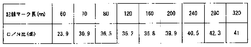
  • the recording mark was formed on the decomposition reaction layer of the optical recording disk sample so that the length of the recording mark was 60 nm 70 nm 80 nm 120 nm 160 nm 200 nm 240 nm 280 nm and 320 nm, respectively, under the following conditions. . At this time, no change was observed in the phase state of the light absorbing layer.
  • the data recorded on the optical recording disk sample was reproduced using the same optical recording medium evaluation device under the following conditions, and the CZN ratio of the reproduced signal was measured.
  • the reproduction power of the laser beam was set to 2. OmW.
  • the C / N ratio of the reproduced signal is 36.8 dB 39.9 dB 40.5 dB 42.3 dB 41. OdB, and when the recording mark is formed by forming an empty space in the arc / reaction layer, only those below the resolution limit can be used. Resolution It has been found that a reproduced signal having a high C / N ratio can be obtained even when data is recorded by forming a recording mark having a length longer than the limit.

Abstract

An optical recording disc capable of recording/reproducing data constituted of a recording mark array including recording marks and blank areas even when the length of the recording marks or the length of the blank area between adjacent recording marks is shorter than a resolution limit, and capable of increasing the recording capacity greatly. The optical recording disc comprises a substrate (2), a third dielectric layer (3), a light absorption layer (4), a second dielectric layer (5), a decomposition reactive layer (6) principally containing a platinum oxide, a first dielectric layer (7), and a light transmitting layer (8), characterized in that the platinum oxide in the decomposition reactive layer (6) is decomposed into platinum and oxygen when the decomposition reactive layer (6) is irradiated with a laser beam (20) through the light transmitting layer (8), cavities are formed by oxygen gas thus produced, and a recording mark is formed on the decomposition reactive layer (6) by fine platinum particles deposited in the cavities.

Description

明 細 書  Specification
光記録ディスク  Optical recording disk
技術分野  Technical field
[0001] 本発明は、光記録ディスクに関するものであり、さらに詳細には、記録マークの長さ や、隣り合う記録マーク間のブランク領域の長さが、解像限界未満である場合にも、こ れらの記録マークおよびブランク領域を含む記録マーク列により構成されたデータを 記録し、再生することができ、記録容量を大幅に増大させることができる光記録デイス クに関するものである。  The present invention relates to an optical recording disk, and more particularly, to a case where the length of a recording mark or the length of a blank area between adjacent recording marks is less than the resolution limit. The present invention relates to an optical recording disk capable of recording and reproducing data composed of a series of recording marks including these recording marks and blank areas, and capable of greatly increasing the recording capacity.
背景技術  Background art
[0002] 従来より、デジタルデータを記録するための記録媒体として、 CDや DVDに代表さ れる光記録ディスクが広く利用されている力 近年においては、より大容量で、かつ、 高いデータ転送レートを有する光記録ディスクの開発が盛んに行われている。  [0002] Conventionally, optical recording disks typified by CDs and DVDs have been widely used as recording media for recording digital data. In recent years, higher capacity and higher data transfer rates have been required. The development of optical recording discs having them is being actively pursued.
[0003] こうした光記録ディスクにおいては、データの記録 ·再生に用いるレーザ光の波長 λを小さくするとともに、対物レンズの開口数 ΝΑを大きくして、レーザ光のビームスポ ット径を小さく絞ることにより、光記録ディスクの記録容量の増大が図られている。 発明の開示  [0003] In such an optical recording disk, the wavelength λ of the laser beam used for recording and reproducing data is reduced, the numerical aperture ΝΑ of the objective lens is increased, and the beam spot diameter of the laser beam is reduced. The recording capacity of an optical recording disk has been increased. Disclosure of the invention
発明が解決しょうとする課題  Problems to be solved by the invention
[0004] 光記録ディスクにおいては、光記録ディスクに記録された記録マークの長さ、およ び、隣り合う記録マーク間の長さ、すなわち、記録マークが形成されていない領域(以 下、「ブランク領域」という。)の長さが解像限界未満になると、光記録ディスクからデ ータを再生することが不可能になる。 [0004] In an optical recording disk, the length of a recording mark recorded on the optical recording disk and the length between adjacent recording marks, that is, an area where no recording mark is formed (hereinafter, referred to as " If the length of the “blank area” is less than the resolution limit, it becomes impossible to reproduce data from the optical recording disk.
[0005] 解像限界は、レーザ光の波長 λと、レーザ光を集束するための対物レンズの開口 数 ΝΑによって決定され、記録マークとブランク領域との繰り返しの周波数、すなわち[0005] The resolution limit is determined by the wavelength λ of the laser light and the numerical aperture の of the objective lens for focusing the laser light, and the repetition frequency of the recording mark and the blank area, that is,
、空間周波数が 2ΝΑΖ λ以上の場合に、記録マークおよびブランク領域に記録され たデータの読み取りが不可能になる。 When the spatial frequency is 2ΝΑΖλ or more, it becomes impossible to read the data recorded in the recording mark and the blank area.
[0006] したがって、読み取り可能な空間周波数に対応する記録マークおよびブランクの長 さは、それぞれ、 λ /4ΝΑ以上となり、波長 λのレーザ光を、開口数 ΝΑの対物レン ズによって、光記録ディスクの表面に集光させるときは、 λ /4ΝΑの長さの記録マー クおよびブランク領域力 読み取ることができる最短の記録マークおよびブランク領域 となる。 [0006] Accordingly, the lengths of the recording mark and the blank corresponding to the readable spatial frequency are each λ / 4ΝΑ or more, and the laser beam having the wavelength λ is supplied to the objective lens having the numerical aperture ΝΑ. When the light is condensed on the surface of the optical recording disk, the recording mark and blank area have a length of λ / 4, and the shortest recording mark and blank area can be read.
[0007] このように、データを再生する場合には、データの再生が可能な解像限界が存在し 、再生することができる記録マークの長さおよびブランク領域の長さに制限がある。し たがって、解像限界未満の長さの記録マークおよびブランク領域を形成して、データ を記録しても、記録されたデータを再生することができないので、光記録ディスクに、 データを記録するときに形成可能な記録マークの長さおよびブランク領域の長さが必 然的に制限されるから、通常は、解像限界未満になるような長さの記録マークおよび ブランク領域を形成して、光記録ディスクにデータを記録することがない。  As described above, when data is reproduced, there is a resolution limit at which data can be reproduced, and there are restrictions on the length of a record mark and the length of a blank area that can be reproduced. Therefore, even if a record mark and blank area with a length less than the resolution limit are formed and data is recorded, the recorded data cannot be reproduced. In some cases, the length of the record mark and blank area that can be formed are necessarily limited, so usually, the record mark and blank area are formed to have a length that is less than the resolution limit. No data is recorded on the optical recording disk.
[0008] したがって、光記録ディスクの記録容量を増大させるためには、データの再生に用 いるレーザ光の波長 λを短くし、あるいは、対物レンズの開口数 ΝΑを大きくすること によって、解像限界を小さくし、より短い記録マークとブランク領域よりなるデータを再 生することができるようにすることが要求される。  [0008] Therefore, in order to increase the recording capacity of an optical recording disk, the resolution limit is reduced by shortening the wavelength λ of the laser beam used for data reproduction or increasing the numerical aperture の of the objective lens. Therefore, it is required to reduce the size of the data and make it possible to reproduce data consisting of shorter recording marks and blank areas.
[0009] し力しながら、データの再生に用いるレーザ光の波長えを短くし、あるいは、対物レ ンズの開口数 ΝΑを大きくすることには限界があり、したがって、解像限界を小さくす ることによって、光記録ディスクの記録容量を増大させることには限界があった。  [0009] There is a limit to shortening the wavelength of the laser beam used for data reproduction or increasing the numerical aperture 対 物 of the objective lens, while reducing the resolution limit. Therefore, there is a limit to increasing the recording capacity of the optical recording disk.
[0010] したがって、本発明の目的は、記録マークの長さや、隣り合う記録マーク間のブラン ク領域の長さが、解像限界未満である場合にも、これらの記録マークおよびブランク 領域を含む記録マーク列により構成されたデータを記録し、再生することができ、記 録容量を大幅に増大させることができる光記録ディスクを提供することにある。  Therefore, an object of the present invention is to include a recording mark and a blank area even when the length of a recording mark or the length of a blank area between adjacent recording marks is less than the resolution limit. An object of the present invention is to provide an optical recording disk capable of recording and reproducing data constituted by a recording mark sequence and capable of greatly increasing a recording capacity.
課題を解決するための手段  Means for solving the problem
[0011] 本発明のかかる目的は、 390nmなレ、し 420nmの波長 λを有するレーザ光が、 0. [0011] The object of the present invention is to provide a laser light having a wavelength λ of 390 nm and a wavelength λ of 420 nm.
7ないし 0. 9の開口数 ΝΑを有する対物レンズによって、集光されて、データが記録さ れ、再生されるように構成された光記録ディスクであって、少なくとも、基板と、前記基 板上に設けられ、 5nmないし lOOnmの厚さを有する第二の誘電体層と、前記第二 の誘電体層上に設けられ、 2nmないし 80nmの厚さを有し、貴金属酸化物を主成分 として含む分解反応層と、前記分解反応層上に設けられる第一の誘電体層と、前記 第一の誘電体層上に設けられ、 10 μ mないし 200 μ mの厚さを有する光透過層とを 備え、前記光透過層を介して、前記レーザ光が照射されたときに、前記分解反応層 に主成分として含まれている前記貴金属酸化物が貴金属と酸素に分解され、生成さ れた酸素ガスによって、空洞が形成されるとともに、前記貴金属の微粒子が前記空洞 内に析出されることによって、前記分解反応層に記録マークが形成されるように構成 されたことを特徴とする光記録ディスクによって達成される。 An optical recording disk configured to be condensed by an objective lens having a numerical aperture of 7 to 0.9 to record and reproduce data, comprising at least a substrate and a substrate. A second dielectric layer having a thickness of 5 nm to 100 nm, and a second dielectric layer provided on the second dielectric layer, having a thickness of 2 nm to 80 nm and containing a noble metal oxide as a main component. A decomposition reaction layer, a first dielectric layer provided on the decomposition reaction layer, A light-transmitting layer provided on the first dielectric layer and having a thickness of 10 μm to 200 μm, wherein when the laser light is irradiated through the light-transmitting layer, the decomposition is performed. The noble metal oxide contained as a main component in the reaction layer is decomposed into a noble metal and oxygen, and a cavity is formed by the generated oxygen gas, and fine particles of the noble metal are precipitated in the cavity. Thus, a recording mark is formed on the decomposition reaction layer.
[0012] 本発明者の研究によれば、少なくとも、基板と、前記基板上に設けられ、 5nmない し lOOnmの厚さを有する第二の誘電体層と、前記第二の誘電体層上に設けられ、 2 nmないし 80nmの厚さを有し、貴金属酸化物を主成分として含む分解反応層と、前 記分解反応層上に設けられる第一の誘電体層と、前記第一の誘電体層上に設けら れ、 10 x mないし 200 z mの厚さを有する光透過層とを備えた光記録ディスクに、 0 . 7ないし 0. 9の開口数 NAを有する対物レンズによって、光透過層を介して、 390η mないし 420nmの波長 λを有するレーザ光を集光すると、分解反応層に主成分とし て含まれている貴金属酸化物が貴金属と酸素に分解され、生成された酸素ガスによ つて、分解反応層内に空洞が形成されるとともに、貴金属の微粒子が空洞内に析出 し、分解反応層に記録マークが形成されて、データが記録され、こうして、データが光 記録ディスクに記録された場合には、記録マーク列を構成する記録マークの長さや、 隣り合う記録マーク間のブランク領域の長さが、解像限界未満であるときにも、 390η mないし 420nmの波長 λを有するレーザ光を、 0· 7ないし 0· 9の開口数 NAを有す る対物レンズを用いて、光透過層を介して、光記録ディスクに集光することによって、 データが再生可能であることが見出されている。  According to the study of the present inventor, at least a substrate, a second dielectric layer provided on the substrate and having a thickness of 5 nm to 100 nm, and a second dielectric layer on the second dielectric layer A decomposition reaction layer having a thickness of 2 nm to 80 nm and containing a noble metal oxide as a main component, a first dielectric layer provided on the decomposition reaction layer, and the first dielectric layer. A light transmitting layer provided on the layer and having a light transmitting layer having a thickness of 10 xm to 200 zm, the light transmitting layer is formed by an objective lens having a numerical aperture NA of 0.7 to 0.9. When laser light having a wavelength λ of 390 ηm or 420 nm is condensed, the noble metal oxide contained as a main component in the decomposition reaction layer is decomposed into noble metal and oxygen, and the generated oxygen gas generates In addition, a cavity is formed in the decomposition reaction layer, and fine particles of noble metal precipitate in the cavity and decompose. When a recording mark is formed on the reaction layer and data is recorded, and thus the data is recorded on the optical recording disc, the length of the recording mark constituting the recording mark row and a blank area between the adjacent recording marks. Is less than the resolution limit, a laser beam having a wavelength λ of 390 η m to 420 nm is irradiated with an objective lens having a numerical aperture NA of 0.7 to 0.9. It has been found that the data can be reproduced by focusing the light on the optical recording disk via the transmission layer.
[0013] 分解反応層に主成分として含まれている貴金属酸化物が貴金属と酸素に分解され 、生成された酸素ガスによって、分解反応層内に空洞が形成されるとともに、貴金属 の微粒子が空洞内に析出し、分解反応層に記録マークが形成されて、データが記録 された場合に、記録マーク列を構成する記録マークの長さや、隣り合う記録マーク間 のブランク領域の長さが、解像限界未満であるときでも、データを再生することができ るという理由は必ずしも明らかではないが、空洞内に析出した貴金属の微粒子に、再 生用のレーザ光が照射されることにより、近接場光が発生し、解像限界がなくなった ためか、あるいは、空洞内に析出した貴金属の微粒子と照射されたレーザ光との相 互作用によって、解像限界が小さくなつたためではないかと推測される。 [0013] The noble metal oxide contained as a main component in the decomposition reaction layer is decomposed into noble metal and oxygen, and the generated oxygen gas forms a cavity in the decomposition reaction layer, and the fine particles of the noble metal fall into the cavity. When the recording marks are formed on the decomposition reaction layer and the data is recorded, the length of the recording marks constituting the recording mark row and the length of the blank area between adjacent recording marks are resolved. Although the reason that data can be reproduced even when the value is less than the limit is not always clear, the near-field light is generated by irradiating the noble metal particles deposited in the cavity with laser light for reproduction. Has occurred and the resolution limit has disappeared. It is speculated that the resolution limit was reduced due to the interaction between the noble metal particles deposited in the cavity and the irradiated laser beam.
[0014] このように、分解反応層に空洞を形成するとともに、貴金属の微粒子を空洞内に析 出させて、分解反応層に記録マークを形成することにより、記録マーク列を構成する 記録マークの長さや、隣り合う記録マーク間のブランク領域の長さが、解像限界未満 であるときでも、データの再生が可能になるから、光記録ディスクに、より高密度に、 データを記録することができ、したがって、光記録ディスクの記憶容量を大幅に増大 させることが可能となる。  [0014] As described above, a cavity is formed in the decomposition reaction layer, and fine particles of a noble metal are precipitated in the cavity to form a recording mark in the decomposition reaction layer. Even when the length or the length of the blank area between adjacent recording marks is less than the resolution limit, data can be reproduced, so it is possible to record data at higher density on an optical recording disc. Therefore, it is possible to greatly increase the storage capacity of the optical recording disk.
[0015] 本発明において、分解反応層に主成分として含まれる貴金属酸化物は、とくに限 定されるものではないが、酸化物の形成し易さ、近接場光の発生効率の観点から、 銀、白金およびパラジウムよりなる群から選ばれる一種の貴金属を含む酸化物が好ま しぐとくに、白金酸化物が、分解温度が高いため、好ましい。  [0015] In the present invention, the noble metal oxide contained as a main component in the decomposition reaction layer is not particularly limited, but from the viewpoint of easy formation of the oxide and generation efficiency of near-field light, silver Oxides containing one kind of noble metal selected from the group consisting of platinum and palladium are particularly preferred, and platinum oxide is preferred because of its high decomposition temperature.
[0016] 本発明の好ましい実施態様においては、貴金属酸化物として、白金酸化物 PtOx が用いられ、光透過層を介して、レーザ光が照射されたときに、白金と酸素とに分解 されるように構成されてレ、る。  [0016] In a preferred embodiment of the present invention, platinum oxide PtOx is used as the noble metal oxide, and is decomposed into platinum and oxygen when irradiated with laser light through the light transmitting layer. It is composed of
[0017] 白金酸化物は、他の貴金属酸化物に比べて、分解温度が高ぐしたがって、記録 用のパワーに設定されたレーザ光を照射して、記録マークを形成する際に、レーザ 光が照射された領域から、周囲の分解反応層に、熱が拡散しても、レーザ光が照射 された領域以外の領域で、白金酸化物の分解反応が生じることが防止されるから、 分解反応層の所望の領域に、空洞を形成して、記録マークを形成することが可能に なる。  [0017] Platinum oxide has a higher decomposition temperature than other noble metal oxides. Therefore, when irradiating a laser beam set to the recording power to form a recording mark, the laser beam is irradiated with the laser beam. Even if heat diffuses from the irradiated area to the surrounding decomposition reaction layer, the decomposition reaction of platinum oxide is prevented from occurring in the area other than the area irradiated with the laser beam. It is possible to form a recording mark by forming a cavity in a desired area.
[0018] また、高いパワーの再生用レーザ光が照射されて、データが再生される場合におい ても、白金酸化物は、他の貴金属酸化物に比べて、分解温度が高いから、白金酸化 物が白金と酸素に分解されるおそれがなぐしたがって、繰り返し、光記録ディスクに 記録されたデータを再生しても、記録マークの形状が変化することはなぐ空洞が形 成され、また、記録マークが形成された領域以外の領域に、新たに空洞が形成される こともないから、光記録ディスクの再生耐久性を向上させることが可能になる。  [0018] In addition, even when data is reproduced by irradiating a high-power reproducing laser beam, platinum oxide has a higher decomposition temperature than other noble metal oxides. Therefore, even if the data recorded on the optical recording disk is repeatedly reproduced, the shape of the recording mark does not change even if the data recorded on the optical recording disk is repeatedly reproduced. Since no new cavity is formed in a region other than the formed region, the reproduction durability of the optical recording disk can be improved.
[0019] 本発明において、記録マークの長さや、隣り合う記録マーク間のブランク領域の長 さが、解像限界未満である場合にも、高い C/N比を有する再生信号を得るために は、 Xが 0. 5以上、 4. 0以下であることが好ましぐ 1. 0以上、 3未満であることがより 好ましい。 In the present invention, the length of a recording mark or the length of a blank area between adjacent recording marks However, in order to obtain a reproduced signal having a high C / N ratio even when the resolution is below the resolution limit, it is preferable that X is 0.5 or more and 4.0 or less 1.0 or more And more preferably less than 3.
[0020] 本発明において、貴金属酸化物として、酸化銀 AgOyを用いる場合には、 yが 0. 5 以上、 1. 5以下であることが好ましぐ 0. 5以上、 1. 0以下であることがより好ましい。  In the present invention, when silver oxide AgOy is used as the noble metal oxide, y is preferably 0.5 or more and 1.5 or less, more preferably 0.5 or more and 1.0 or less. Is more preferable.
[0021] 本発明において、好ましくは、白金酸化物が分解して、形成される白金の微粒子は 、分解反応層に形成すべき空洞の大きさよりも小さい粒径を有しており、白金酸化物 が分解して、形成される白金の微粒子が、通常、形成される空洞の大きさに比べて十 分に小さい場合には、空洞内に析出した白金の微粒子によって、空洞の形状が悪影 響を受け、記録マークの形状に、望ましくない変化が生じることを効果的に防止する ことが可能になる。  In the present invention, preferably, the platinum fine particles formed by decomposition of platinum oxide have a particle size smaller than the size of a cavity to be formed in the decomposition reaction layer, When the fine particles of platinum formed by the decomposition of platinum are usually sufficiently smaller than the size of the cavity to be formed, the shape of the cavity is adversely affected by the fine particles of platinum deposited in the cavity. As a result, it is possible to effectively prevent an undesirable change in the shape of the recording mark.
[0022] 本発明において、好ましくは、光記録ディスクは、さらに、さらに、前記基板と前記第 二の誘電体層との間に、 10nmないし 140nmの層厚を有する第三の誘電体層と、前 記第三の誘電体層上に設けられ、 5nmないし lOOnmの層厚を有する光吸収層とを 備え、前記光吸収層が、前記光透過層を介して、前記レーザ光が照射されたときに、 前記レーザ光を吸収して、発熱するように構成されてレ、る。  In the present invention, preferably, the optical recording disk further comprises a third dielectric layer having a thickness of 10 nm to 140 nm between the substrate and the second dielectric layer, A light absorbing layer provided on the third dielectric layer and having a layer thickness of 5 nm to 100 nm, wherein the light absorbing layer is irradiated with the laser light through the light transmitting layer. The laser beam is absorbed to generate heat.
[0023] 基板と第二の誘電体層との間に、第三の誘電体層と、光吸収層が形成され、光透 過層を介して、レーザ光が照射されたときに、光吸収層がレーザ光を吸収して、発熱 するように構成されている場合には、レーザ光が照射されたときに、分解反応層自身 が発熱し難くても、光吸収層から伝達される熱によって、分解反応層に主成分として 含まれている貴金属酸化物を貴金属と酸素に分解させることができ、したがって、分 解反応層が容易に変形しやすくなるように、分解反応層を薄層化しても、また、分解 反応層が、レーザ光の透過性の高い貴金属酸化物を含んでいても、光記録ディスク に、レーザ光を照射することにより、所望のように、貴金属酸化物を分解させて、記録 マークを形成することが可能になる。  A third dielectric layer and a light-absorbing layer are formed between the substrate and the second dielectric layer, and when a laser beam is irradiated through the light-transmitting layer, the light is absorbed. When the layer is configured to absorb laser light and generate heat, even when the decomposition reaction layer itself is unlikely to generate heat when irradiated with laser light, heat is transferred from the light absorption layer. However, the noble metal oxide contained as a main component in the decomposition reaction layer can be decomposed into noble metal and oxygen, and therefore, the decomposition reaction layer is thinned so that the decomposition reaction layer is easily deformed. Also, even if the decomposition reaction layer contains a noble metal oxide having high laser light transmission properties, the noble metal oxide is decomposed as desired by irradiating the optical recording disk with the laser light. Thus, a recording mark can be formed.
[0024] 本発明において、光吸収層は、レーザ光の吸収率が高ぐ熱伝導率の低い材料を 含んでレ、ることが好ましく、 Sbおよび Teの少なくとも一方を含んでレ、ることが好ましレヽ [0025] 本発明において、光吸収層に含まれる Sbおよび Teの少なくとも一方を含む合金と しては、(Sb Te ) M、または { (GeTe) (Sb Te ) } M で表わされる組成 a 1-a 1-b b c 2 3 1— c d 1-d を有するものがとくに好ましい。ここに、 Mは、 Sb、 Teおよび Geを除く元素を表わす。 [0024] In the present invention, the light absorbing layer preferably contains a material having a high absorptivity for laser light and a low thermal conductivity, and preferably contains at least one of Sb and Te. I like it [0025] In the present invention, the alloy containing at least one of Sb and Te contained in the light absorbing layer includes (a) a composition represented by (SbTe) M or {(GeTe) (SbTe)} M. Those having -a 1-bbc 2 3 1—cd 1-d are particularly preferred. Here, M represents an element excluding Sb, Te and Ge.
[0026] 光吸収層に含まれる Sbおよび Teの少なくとも一方を含む合金が、 (Sb Te ) a 1一 a 1一 b[0026] The alloy containing at least one of Sb and Te contained in the light absorbing layer is (Sb Te) a 1 a 1 a 1 b
Mで表される組成を有するもののときは、 aおよび bは、 0≤a≤l ,かつ、 0≤b≤0. 2 b For those having the composition represented by M, a and b are 0≤a≤l, and 0≤b≤0.2 b
5であることが好ましレ、。 bが 0. 25を越えているときは、光の吸収係数が光吸収層に 要求される値よりも低くなり、また、熱伝導性が光吸収層に要求される値よりも低くなり 、好ましくない。  Les, preferably to be 5. When b exceeds 0.25, the light absorption coefficient is lower than the value required for the light absorbing layer, and the thermal conductivity is lower than the value required for the light absorbing layer. Absent.
[0027] 一方、光吸収層に含まれる Sbおよび Teの少なくとも一方を含む合金力 { (GeTe)  [0027] On the other hand, the alloy force containing at least one of Sb and Te contained in the light absorbing layer {(GeTe)
(Sb Te ) } M で表される組成を有するもののときは、 l/3≤c≤2/3,かつ、 c 2 3 1-c d 1-d  (Sb Te)} If it has a composition represented by M, l / 3≤c≤2 / 3, and c 2 3 1-c d 1-d
0. 9≤dに設定することが好ましい。  It is preferable to set 0.9≤d.
[0028] 元素 Mは、とくに限定されるものではなレ、が、 In、 Ag、 Au、 Bi、 Se、 Al、 P、 H、 Si、 C、 V、 W、 Ta、 Zn、 Mn、 Ti、 Sn、 Pb、 Pd、 N、〇および希土類元素(Sc、 Yおよびラ ンタノイド)よりなる群から選ばれる少なくとも 1種の元素を主成分として含むことが好 ましレ、。とくに、 390nmないし 420nmの波長 λを有するレーザ光を用いる場合には 、元素 Μとして、 Ag、 Inおよび希土類元素よりなる群から選ばれる少なくとも一種の 元素を主成分として含むことが好ましレ、。  [0028] The element M is not particularly limited, but In, Ag, Au, Bi, Se, Al, P, H, Si, C, V, W, Ta, Zn, Mn, Ti, It preferably contains at least one element selected from the group consisting of Sn, Pb, Pd, N, 〇 and rare earth elements (Sc, Y and lanthanoids) as a main component. In particular, when laser light having a wavelength λ of 390 nm to 420 nm is used, it is preferable that the element 含 む contains at least one element selected from the group consisting of Ag, In and rare earth elements as a main component.
[0029] 本発明において、第三の誘電体層と、光吸収層とを設けない場合には、分解反応 層は、 20nmないし 80nmの厚さを有するように形成されることが好ましい。  [0029] In the present invention, when the third dielectric layer and the light absorbing layer are not provided, the decomposition reaction layer is preferably formed to have a thickness of 20 nm to 80 nm.
[0030] 分解反応層は、レーザ光の透過性が高い貴金属酸化物を主成分として含んでいる ため、分解反応層の厚さが、 20nm未満である場合には、レーザ光の吸収率が低ぐ レーザ光が照射されても、分解反応層が十分に加熱されず、所望のように、貴金属 酸化物の分解反応を生じさせることができない場合があり、好ましくない。  [0030] Since the decomposition reaction layer mainly contains a noble metal oxide having high laser light transmittance, when the thickness of the decomposition reaction layer is less than 20 nm, the absorption rate of the laser light is low. Even if the laser beam is irradiated, the decomposition reaction layer is not sufficiently heated, and the decomposition reaction of the noble metal oxide may not be caused as desired, which is not preferable.
[0031] 一方、本発明において、第三の誘電体層と、光吸収層とを、基板と第二の誘電体 層との間に設ける場合には、レーザ光の照射を受けたときに、分解反応層自身が、 発熱する必要がないので、連続膜として形成することができる範囲で、分解反応層を 薄く形成することができ、分解反応層は、 2nmないし 50nmの厚さを有するように形 成されることが好ましい。 [0032] 本発明において、レーザ光が照射されて、分解反応層が、貴金属と酸素に分解し、 空洞が形成される際に、第二の誘電体層および光吸収層が変形することが好ましい On the other hand, in the present invention, when the third dielectric layer and the light absorbing layer are provided between the substrate and the second dielectric layer, when the third dielectric layer and the second dielectric layer are irradiated with laser light, Since the decomposition reaction layer itself does not need to generate heat, the decomposition reaction layer can be formed as thin as possible to the extent that it can be formed as a continuous film, and the decomposition reaction layer should have a thickness of 2 nm to 50 nm. Preferably, it is formed. [0032] In the present invention, it is preferable that the second dielectric layer and the light absorbing layer be deformed when the decomposition reaction layer is irradiated with laser light to be decomposed into noble metal and oxygen, and a cavity is formed.
[0033] 第二の誘電体層および光吸収層が変形した領域は、第二の誘電体層および光吸 収層が変形しない領域と、光学特性が異なるので、再生信号の CZN比をより一層 向上させることができる。 The region where the second dielectric layer and the light absorbing layer are deformed has different optical characteristics from the region where the second dielectric layer and the light absorbing layer are not deformed, so that the CZN ratio of the reproduced signal is further increased. Can be improved.
発明の効果  The invention's effect
[0034] 本発明によれば、記録マークの長さや、隣り合う記録マーク間のブランク領域の長 さが、解像限界未満である場合にも、これらの記録マークおよびブランク領域を含む 記録マーク列により構成されたデータを記録し、再生することができ、記録容量を大 幅に増大させることができる光記録ディスクを提供することが可能になる。  According to the present invention, even when the length of a recording mark or the length of a blank area between adjacent recording marks is less than the resolution limit, a recording mark sequence including these recording marks and the blank area Thus, it is possible to provide an optical recording disk capable of recording and reproducing the data constituted by the above, and capable of greatly increasing the recording capacity.
図面の簡単な説明  Brief Description of Drawings
[0035] [図 1]図 1は、本発明の好ましい実施態様に力かる光記録ディスクの略断面図である [図 2]図 2は、図 1の Aで示された部分の略拡大断面図である。  FIG. 1 is a schematic cross-sectional view of an optical recording disk according to a preferred embodiment of the present invention. FIG. 2 is a schematic enlarged cross-sectional view of a portion indicated by A in FIG. FIG.
[図 3]図 3 (a)は、データが記録される前の光記録ディスクの一部拡大略断面図であり 、図 3 (b)は、データが記録された後の光記録ディスクの一部拡大略断面図である。  FIG. 3 (a) is a partially enlarged schematic cross-sectional view of an optical recording disk before data is recorded, and FIG. 3 (b) is an optical recording disk after data is recorded. It is a part enlarged schematic sectional view.
[図 4]図 4は、本発明の別の好ましい実施態様に力かる光記録ディスクの略斜視図で ある。  FIG. 4 is a schematic perspective view of an optical recording disk according to another preferred embodiment of the present invention.
[図 5]図 5は、図 4の Bで示された部分の略拡大断面図である。  FIG. 5 is a schematic enlarged sectional view of a portion indicated by B in FIG. 4.
符号の説明  Explanation of symbols
[0036] 1 光記録ディスク [0036] 1 Optical recording disk
2 基板  2 Board
3 第三の誘電体層  3 Third dielectric layer
4 光吸収層  4 Light absorption layer
5 第二の誘電体層  5 Second dielectric layer
6 分解反応層  6 Decomposition reaction layer
7 第一の誘電体層 8 光透過層 7 First dielectric layer 8 Light transmission layer
10 光記録ディスク  10 Optical recording disc
20 レーザ光  20 Laser light
発明を実施するための最良の形態  BEST MODE FOR CARRYING OUT THE INVENTION
[0037] 以下、添付図面に基づいて、本発明の好ましい実施態様につき、詳細に説明をカロ る。 Hereinafter, preferred embodiments of the present invention will be described in detail with reference to the accompanying drawings.
[0038] 図 1は、本発明の好ましい実施態様に力かる光記録ディスクの略斜視図であり、図 2は、図 1に示された光記録ディスクのトラックに沿った断面のうち、 Aで示される部分 の略拡大断面図である。  FIG. 1 is a schematic perspective view of an optical recording disk according to a preferred embodiment of the present invention, and FIG. 2 is a cross-sectional view of the optical recording disk shown in FIG. It is a substantially enlarged sectional view of the part shown.
[0039] 図 1および図 2に示されるように、本実施態様にかかる光記録媒体 1は、基板 2を備 え、基板 2上に、第三の誘電体層 3と、光吸収層 4と、第二の誘電体層 5と、分解反応 層 6と、第一の誘電体層 7と、光透過層 8とが、この順に、積層されている。  As shown in FIGS. 1 and 2, the optical recording medium 1 according to the present embodiment includes a substrate 2, and a third dielectric layer 3 and a light absorbing layer 4 are provided on the substrate 2. The second dielectric layer 5, the decomposition reaction layer 6, the first dielectric layer 7, and the light transmitting layer 8 are laminated in this order.
[0040] 本実施態様においては、図 1に示されるように、光記録ディスク 1は、光透過層 8側 から、レーザ光 20が照射されて、データが記録され、記録されたデータが再生される ように構成されている。レーザ光 20は、 390nmないし 420nmの波長 λを有し、開口 数 ΝΑが 0. 7ないし 0. 9の対物レンズによって、光記録ディスク 1に集光される。  In the present embodiment, as shown in FIG. 1, the optical recording disk 1 is irradiated with laser light 20 from the light transmitting layer 8 side, data is recorded, and the recorded data is reproduced. It is configured to The laser beam 20 has a wavelength λ of 390 nm to 420 nm and is focused on the optical recording disk 1 by an objective lens having a numerical aperture ΝΑ of 0.7 to 0.9.
[0041] 基板 2は、光記録ディスク 1に求められる機械的強度を確保するための支持体とし て、機能する。  The substrate 2 functions as a support for securing the mechanical strength required for the optical recording disk 1.
[0042] 基板 2を形成するための材料は、光記録ディスク 1の支持体として機能することがで きれば、とくに限定されるものではなレ、。基板 2は、たとえば、ガラス、セラミックス、樹 脂などによって、形成すること力 Sできる。これらのうち、成形の容易性の観点から、樹 脂が好ましく使用される。このような樹脂としては、ポリカーボネート樹脂、アクリル樹 脂、エポキシ樹脂、ポリスチレン樹脂、ポリエチレン樹脂、ポリプロピレン樹脂、シリコ ーン樹脂、フッ素系樹脂、 ABS樹脂、ウレタン樹脂などが挙げられる。これらの中でも 、加工性、光学特性などの点から、ポリカーボネート樹脂がとくに好ましい。  [0042] The material for forming the substrate 2 is not particularly limited as long as it can function as a support for the optical recording disk 1. The substrate 2 can be formed by, for example, glass, ceramics, resin, or the like. Of these, resins are preferably used from the viewpoint of ease of molding. Examples of such a resin include a polycarbonate resin, an acrylic resin, an epoxy resin, a polystyrene resin, a polyethylene resin, a polypropylene resin, a silicone resin, a fluorine-based resin, an ABS resin, and a urethane resin. Among these, polycarbonate resins are particularly preferable in terms of processability, optical characteristics, and the like.
[0043] 本実施態様においては、基板 2は、ポリカーボネート樹脂によって形成され、約 1. lmmの厚さを有している。  In this embodiment, the substrate 2 is formed of a polycarbonate resin and has a thickness of about 1. 1 mm.
[0044] 図 2に示されるように、基板 2の表面には、第三の誘電体層 3が形成されている。 [0045] 本実施態様においては、第三の誘電体層 3は、基板 2を保護するとともに、その上 に形成される光吸収層 4を、機能的、化学的に保護する機能を有している。 As shown in FIG. 2, a third dielectric layer 3 is formed on the surface of the substrate 2. In this embodiment, the third dielectric layer 3 has a function of protecting the substrate 2 and a function of functionally and chemically protecting the light absorbing layer 4 formed thereon. I have.
[0046] 第三の誘電体層 3を形成するための誘電体材料は、とくに限定されるものではなく 、たとえば、酸化物、硫化物、窒化物またはこれらの組み合わせを主成分とする誘電 体材料によって、第三の誘電体層 3を形成することができ、第三の誘電体層 3は、好 ましくは、 Si、 Zn、 Al、 Ta、 Ti、 Co、 Zr、 Pb、 Ag、 Zn、 Sn、 Ca、 Ce、 V、 Cu、 Fe、 M gよりなる群から選ばれる少なくとも一種の金属を含む酸化物、窒化物、硫化物、フッ 化物、あるいは、これらの複合物によって形成される。  [0046] The dielectric material for forming the third dielectric layer 3 is not particularly limited. For example, a dielectric material mainly composed of an oxide, a sulfide, a nitride, or a combination thereof is used. Can form the third dielectric layer 3, and the third dielectric layer 3 is preferably made of Si, Zn, Al, Ta, Ti, Co, Zr, Pb, Ag, Zn, It is formed of an oxide, nitride, sulfide, fluoride containing at least one metal selected from the group consisting of Sn, Ca, Ce, V, Cu, Fe, and Mg, or a composite thereof.
[0047] 第三の誘電体層 3は、たとえば、第三の誘電体層 3の構成元素を含む化学種を用 いた気相成長法によって、基板 2の表面上に形成することができる。気相成長法とし ては、真空蒸着法、スパッタリング法などが挙げられる。  The third dielectric layer 3 can be formed on the surface of the substrate 2 by, for example, a vapor growth method using a chemical species containing a constituent element of the third dielectric layer 3. Examples of the vapor deposition method include a vacuum deposition method and a sputtering method.
[0048] 第三の誘電体層 3の厚さは、とくに限定されるものではないが、 10nmないし 140η mが好ましい。  [0048] The thickness of the third dielectric layer 3 is not particularly limited, but is preferably from 10 nm to 140 ηm.
[0049] 図 2に示されるように、第三の誘電体層 3の表面上には、光吸収層 4が形成されて いる。  As shown in FIG. 2, a light absorption layer 4 is formed on the surface of the third dielectric layer 3.
[0050] 本実施態様において、光吸収層 4は、光記録ディスク 1に、記録用のパワーに設定 されたレーザ光 20が照射されたときに、レーザ光 20を吸収して、発熱し、生成した熱 を、後述する分解反応層 6に伝達する機能を有している。  [0050] In the present embodiment, when the optical recording disk 1 is irradiated with the laser beam 20 set to the recording power, the light absorbing layer 4 absorbs the laser beam 20, generates heat, and generates light. It has a function of transmitting the generated heat to a decomposition reaction layer 6 described later.
[0051] 本実施態様においては、光吸収層 4は、光の吸収係数が高ぐ熱伝導率の低い Sb および Teの少なくとも一方を含む合金によって形成されている。  In the present embodiment, the light absorbing layer 4 is made of an alloy containing at least one of Sb and Te having a high light absorption coefficient and a low thermal conductivity.
[0052] Sbおよび Teの少なくとも一方を含む合金としては、 Sb Te ) M、または { (Ge a 1一 a 1一 b b  [0052] The alloy containing at least one of Sb and Te is Sb Te) M or {(Ge a 1 a 1 b b
Te) (Sb Te ) } M で表わされる組成を有するものがとくに好ましレ、。ここに、 M c 2 3 1-c d 1-d  Te) (Sb Te)} Those having a composition represented by M are particularly preferred. Where M c 2 3 1-c d 1-d
は、 Sb、 Teおよび Geを除く元素を表わす。  Represents an element other than Sb, Te and Ge.
[0053] 光吸収層 4に含まれる Sbおよび Teの少なくとも一方を含む合金力 S、(Sb Te ) Mで表される組成を有するもののときは、 0≤a≤l . 0≤b≤0. 25であることが好ま b [0053] When the alloying force S containing at least one of Sb and Te contained in the light absorbing layer 4 has a composition represented by (SbTe) M, 0≤a≤l. 0≤b≤0. Preferably 25
しい。 bが 0. 25を越えているときは、光の吸収係数が光吸収層 4に要求される値より も低くなり、また、熱伝導性が光吸収層 4に要求される値よりも低くなり、好ましくない。  That's right. When b exceeds 0.25, the light absorption coefficient becomes lower than the value required for the light absorbing layer 4, and the thermal conductivity becomes lower than the value required for the light absorbing layer 4. Is not preferred.
[0054] 一方、光吸収層 4に含まれる Sbおよび Teの少なくとも一方を含む合金力 S、 { (GeTe ) (Sb Te ) } M で表される組成を有するもののときは、 l/3≤c≤2/3,かつ c 2 3 1-c d 1-d On the other hand, the alloying force S containing at least one of Sb and Te contained in the light absorbing layer 4, {(GeTe ) (Sb Te)} If the composition is represented by M, l / 3≤c≤2 / 3, and c 2 3 1-cd 1-d
、 0. 9≤dであることが好ましい。  , 0.9≤d.
[0055] 元素 Mは、とくに限定されるものではないが、 In、 Ag、 Au、 Bi、 Se、 Al、 P、 H、 Si、 C、 V、 W、 Ta、 Zn、 Mn、 Ti、 Sn、 Pb、 Pd、 N、〇および希土類元素(Sc、 Yおよびラ ンタノイド)よりなる群から選ばれる少なくとも 1種の元素を主成分として含むことが好 ましレ、。とくに、 390nmないし 420nmの波長 λを有するレーザ光を用いる場合には 、元素 Μとして、 Ag、 Inおよび希土類元素よりなる群から選ばれる少なくとも一種の 元素を主成分として含むことが好ましレ、。  [0055] The element M is not particularly limited, but In, Ag, Au, Bi, Se, Al, P, H, Si, C, V, W, Ta, Zn, Mn, Ti, Sn, It preferably contains at least one element selected from the group consisting of Pb, Pd, N, 〇 and rare earth elements (Sc, Y and lanthanoids) as a main component. In particular, when laser light having a wavelength λ of 390 nm to 420 nm is used, it is preferable that the element 含 む contains at least one element selected from the group consisting of Ag, In and rare earth elements as a main component.
[0056] 本実施形態において、光吸収層 4は、光吸収層 4の構成元素を含む化学種を用い た気相成長法によって、第三の誘電体層 3の表面上に形成することができ、気相成 長法としては、真空蒸着法、スパッタリング法などが挙げられる。  In the present embodiment, the light absorbing layer 4 can be formed on the surface of the third dielectric layer 3 by a vapor growth method using a chemical species containing a constituent element of the light absorbing layer 4. Examples of the vapor phase growth method include a vacuum deposition method and a sputtering method.
[0057] 光吸収層 4は、 5nmないし lOOnmの厚さを有していることが好ましレ、。光吸収層 4 の厚さ力 5nm未満である場合には、光吸収率が低すぎ、一方、光吸収層 4の厚さ 力 lOOnmを越えると、後述のように、分解反応層 6に空洞が形成される際に、光吸 収層 4が変形し難くなり、好ましくない。  [0057] The light absorbing layer 4 preferably has a thickness of 5 nm to 100 nm. If the thickness of the light absorbing layer 4 is less than 5 nm, the light absorption is too low.On the other hand, if the thickness of the light absorbing layer 4 exceeds 100 nm, a cavity is formed in the decomposition reaction layer 6 as described later. When formed, the light absorbing layer 4 is not easily deformed, which is not preferable.
[0058] 図 2に示されるように、光吸収層 4の表面上には、第二の誘電体層 5が形成されて いる。  As shown in FIG. 2, a second dielectric layer 5 is formed on the surface of the light absorption layer 4.
[0059] 本実施態様において、第二の誘電体層 5は、後述する第一の誘電体層 7とともに、 後述する分解反応層 6を、機械的、化学的に保護する機能を有している。  In the present embodiment, the second dielectric layer 5 has a function of mechanically and chemically protecting the decomposition reaction layer 6 described later together with the first dielectric layer 7 described later. .
[0060] 第二の誘電体層 5を形成するための材料は、とくに限定されるものではなぐたとえ ば、酸化物、硫化物、窒化物またはこれらの組み合わせを主成分とする誘電体材料 によって、第三の誘電体層 3を形成することができ、第三の誘電体層 3は、好ましくは 、 Si、 Zn、 Al、 Ta、 Ti、 Co、 Zr、 Pb、 Ag、 Zn、 Sn、 Ca、 Ce、 V、 Cu、 Fe、 Mgよりな る群から選ばれる少なくとも一種の金属を含む酸化物、窒化物、硫化物、フッ化物、 あるいは、これらの複合物によって形成される。  [0060] The material for forming the second dielectric layer 5 is not particularly limited. For example, a dielectric material mainly composed of an oxide, a sulfide, a nitride, or a combination thereof, The third dielectric layer 3 can be formed, and the third dielectric layer 3 is preferably formed of Si, Zn, Al, Ta, Ti, Co, Zr, Pb, Ag, Zn, Sn, Ca, It is formed by oxides, nitrides, sulfides, fluorides, or composites containing at least one metal selected from the group consisting of Ce, V, Cu, Fe, and Mg.
[0061] 第二の誘電体層 5は、第二の誘電体層 5の構成元素を含む化学種を用いた気相成 長法によって、光吸収層 4の表面上に形成することができ、気相成長法としては、真 空蒸着法、スパッタリング法などが挙げられる。 [0062] 第二の誘電体層 5は、好ましくは、 5nmないし lOOnmの厚さを有するように形成さ れる。 [0061] The second dielectric layer 5 can be formed on the surface of the light absorption layer 4 by a vapor phase growth method using a chemical species containing a constituent element of the second dielectric layer 5, Examples of the vapor deposition method include a vacuum evaporation method and a sputtering method. [0062] The second dielectric layer 5 is preferably formed to have a thickness of 5 nm to 100 nm.
[0063] 図 2に示されるように、第二の誘電体層 5の表面上には、分解反応層 6が形成され ている。  As shown in FIG. 2, a decomposition reaction layer 6 is formed on the surface of the second dielectric layer 5.
[0064] 本実施態様においては、分解反応層 6は、記録層の一部として用いられ、光記録 ディスク 1にデータが記録される際に、分解反応層 6に、記録マークが形成される。  In the present embodiment, the decomposition reaction layer 6 is used as a part of the recording layer, and when data is recorded on the optical recording disk 1, a recording mark is formed on the decomposition reaction layer 6.
[0065] 本実施態様において、分解反応層 6は、白金酸化物 PtOxを主成分として含んで いる。  [0065] In this embodiment, the decomposition reaction layer 6 contains platinum oxide PtOx as a main component.
[0066] 本実施態様において、記録マークの長さや、隣り合う記録マーク間のブランク領域 の長さが、解像限界未満である場合にも、高い CZN比を有する再生信号を得るた めには、 1. 0≤x< 3. 0であることがより好ましい。  In the present embodiment, even when the length of a recording mark or the length of a blank area between adjacent recording marks is less than the resolution limit, it is necessary to obtain a reproduced signal having a high CZN ratio. It is more preferable that 1.0 ≦ x <3.0.
[0067] 分解反応層 6は、分解反応層 6に主成分として含まれる構成元素を含む化学種を 用いた気相成長法によって、第二の誘電体層 5の表面上に形成することができ、気 相成長法としては、真空蒸着法、スパッタリング法などが挙げられる。  The decomposition reaction layer 6 can be formed on the surface of the second dielectric layer 5 by a vapor phase growth method using a chemical species containing a constituent element contained as a main component in the decomposition reaction layer 6. Examples of the vapor phase growth method include a vacuum deposition method and a sputtering method.
[0068] 分解反応層 6は、 2nmないし 50nmの厚さを有するように形成されることが好ましい  [0068] The decomposition reaction layer 6 is preferably formed to have a thickness of 2 nm to 50 nm.
[0069] 図 2に示されるように、分解反応層 6の表面上には、第一の誘電体層 7が形成され ている。 As shown in FIG. 2, a first dielectric layer 7 is formed on the surface of the decomposition reaction layer 6.
[0070] 本実施態様において、第一の誘電体層 7は、分解反応層 6を機械的、化学的に保 護する機能を有している。  [0070] In the present embodiment, the first dielectric layer 7 has a function of mechanically and chemically protecting the decomposition reaction layer 6.
[0071] 第一の誘電体層 7を形成するための材料はとくに限定されるものではないが、 Si、 Z n、 Al、 Ta、 Ti、 Co、 Zr、 Pb、 Ag、 Zn、 Sn、 Ca、 Ce、 V、 Cu、 Fe、 Mgよりなる群力、ら 選ばれる少なくとも一種の金属を含む酸化物、窒化物、硫化物、フッ化物、あるいは[0071] Materials for forming the first dielectric layer 7 are not particularly limited, but include Si, Zn, Al, Ta, Ti, Co, Zr, Pb, Ag, Zn, Sn, and Ca. Oxides, nitrides, sulfides, fluorides containing at least one metal selected from the group consisting of, Ce, V, Cu, Fe, Mg, or
、これらの複合物から形成されることが好ましい。 Is preferably formed from these composites.
[0072] 第一の誘電体層 7は、第一の誘電体層 7の構成元素を含む化学種を用いた気相成 長法によって、分解反応層 6の表面上に形成することができ、気相成長法としては、 真空蒸着法、スパッタリング法などが挙げられる。 [0072] The first dielectric layer 7 can be formed on the surface of the decomposition reaction layer 6 by a vapor phase growth method using a chemical species containing a constituent element of the first dielectric layer 7, Examples of the vapor deposition method include a vacuum deposition method and a sputtering method.
[0073] 図 2に示されるように、第一の誘電体層 7の表面上には、光透過層 8が形成されて いる。 As shown in FIG. 2, a light transmitting layer 8 is formed on the surface of the first dielectric layer 7. Yes.
[0074] 光透過層 8は、レーザ光 20が透過する層であり、その表面は、レーザ光 20の入射 面を形成している。  The light transmitting layer 8 is a layer through which the laser light 20 passes, and the surface thereof forms an incident surface of the laser light 20.
[0075] 光透過層 8は、 10 z mないし 200 μ ΐηの厚さを有していることが好ましぐより好まし くは、光透過層 8は、 50 x mなレヽし 150 z mの厚さを有してレヽる。  [0075] More preferably, the light transmitting layer 8 has a thickness of 10 zm to 200 μΐη, and more preferably, the light transmitting layer 8 has a thickness of 50 xm and a thickness of 150 zm. With
[0076] 光透過層 8を形成するための材料は、光学的に透明で、使用されるレーザ光 20の 波長領域である 390nmないし 420nmでの光学吸収および反射が少なぐ複屈折が 小さい材料であれば、とくに限定されるものではなぐスピンコーティング法などによつ て、光透過層 8が形成される場合には、紫外線硬化型樹脂、電子線硬化型樹脂、熱 硬化型樹脂などが、光透過層 8を形成するために用いられ、紫外線硬化型樹脂、電 子線硬化型樹脂などの活性エネルギー線硬化型樹脂が、光透過層 8を形成するた めに、とくに好ましく使用される。  The material for forming the light transmitting layer 8 is a material that is optically transparent, has low optical absorption and reflection in the wavelength region of 390 nm to 420 nm of the laser beam 20 used, and has low birefringence. If the light-transmitting layer 8 is formed by a spin coating method or the like that is not particularly limited, if the light-transmitting layer 8 is formed, an ultraviolet curable resin, an electron beam curable resin, a thermosetting resin, etc. An active energy ray-curable resin such as an ultraviolet ray-curable resin or an electron beam-curable resin is particularly preferably used to form the light-transmitting layer 8.
[0077] 光透過層 8は、第一の誘電体層 7の表面に、光透過性樹脂によって形成されたシ ートを、接着剤を用いて、接着することによって、形成されてもよい。  The light transmitting layer 8 may be formed by bonding a sheet formed of a light transmitting resin to the surface of the first dielectric layer 7 using an adhesive.
[0078] 光透過層 8の膜厚は、スピンコーティング法により、光透過層 8を形成する場合には 、 10 /i mないし 200 μ ΐηが好ましぐ光透過性樹脂によって形成されたシートを、接 着剤を用いて、第一の誘電体層 7の表面に接着して、光透過層 8を形成する場合に は 50 μ mなレ、し 150 μ mが好ましレヽ。  [0078] When the light transmitting layer 8 is formed by a spin coating method, the thickness of the light transmitting layer 8 is preferably 10 / im or 200 μΐη. When the light transmitting layer 8 is formed by adhering to the surface of the first dielectric layer 7 using an adhesive, the thickness is preferably 50 μm, and more preferably 150 μm.
[0079] 以上のように構成された光記録ディスク 1には、次のようにして、データが記録され、 データが再生される。  [0079] Data is recorded on and reproduced from the optical recording disk 1 configured as described above as follows.
[0080] 図 3 (a)は、データが記録される前の光記録ディスク 1の一部拡大略断面図であり、 図 3 (b)は、データが記録された後の光記録ディスク 1の一部拡大略断面図である。  FIG. 3A is a partially enlarged schematic cross-sectional view of the optical recording disk 1 before data is recorded, and FIG. 3B is a diagram of the optical recording disk 1 after data is recorded. It is a partially expanded schematic sectional view.
[0081] 光記録ディスク 1にデータを記録するに際しては、光透過層 8を介して、光記録ディ スク 1にレーザ光 20が照射される。  When data is recorded on the optical recording disk 1, the laser beam 20 is applied to the optical recording disk 1 via the light transmitting layer 8.
[0082] 本実施態様においては、データを高い記録密度で記録するため、 390nmないし 4 20nmの波長 λを有するレーザ光 20を、 0. 7ないし 0. 9の開口数 ΝΑを有する対物 レンズによって、光記録ディスク 1に集光するように構成されてレ、る。  In the present embodiment, in order to record data at a high recording density, the laser beam 20 having a wavelength λ of 390 nm to 420 nm is irradiated by an objective lens having a numerical aperture の of 0.7 to 0.9. It is configured to focus light on the optical recording disk 1.
[0083] また、レーザ光 20のパワーは、 4mWより高く、 12mW以下に設定される。ここに、レ 一ザ光 20のパワーは、光記録ディスク 1の表面におけるレーザ光 20のパワーとして、 定義される。 [0083] The power of the laser light 20 is set to be higher than 4 mW and equal to or lower than 12 mW. Here, The power of the laser beam 20 is defined as the power of the laser beam 20 on the surface of the optical recording disk 1.
[0084] 記録用のパワーに設定されたレーザ光 20が、光記録ディスク 1に照射されると、光 吸収層 4が光の吸収係数が高い Sbおよび Teの少なくとも一方を含む合金によって 形成されているため、レーザ光 20が照射された光吸収層 4の領域が加熱される。  When the laser beam 20 set at the recording power is applied to the optical recording disk 1, the light absorbing layer 4 is formed of an alloy containing at least one of Sb and Te having a high light absorption coefficient. Therefore, the region of the light absorption layer 4 irradiated with the laser beam 20 is heated.
[0085] 光吸収層 4で生成された熱は、分解反応層 6に伝達され、分解反応層 6の温度が 上昇する。  [0085] The heat generated in light absorbing layer 4 is transmitted to decomposition reaction layer 6, and the temperature of decomposition reaction layer 6 rises.
[0086] 分解反応層 6に主成分として含まれる白金酸化物は、レーザ光 20に対する透過性 が高いため、レーザ光 20が照射されても、分解反応層 6自体は発熱し難ぐ 5nmな レ、し lOOnmの厚さを有する分解反応層 6の温度を、白金酸化物の分解温度以上に 上昇させることは困難であるが、本実施態様においては、光の吸収係数が高い Sbお よび Teの少なくとも一方を含む合金によって形成された光吸収層 4が設けられている から、光透過層 6が発熱し、光吸収層 4で生成された熱が、分解反応層 6に伝達され 、分解反応層 6の温度が上昇する。  [0086] Platinum oxide contained as a main component in the decomposition reaction layer 6 has a high transparency to the laser beam 20, so that even when the laser beam 20 is irradiated, the decomposition reaction layer 6 itself hardly generates heat. However, it is difficult to raise the temperature of the decomposition reaction layer 6 having a thickness of 100 nm above the decomposition temperature of platinum oxide, but in the present embodiment, Sb and Te having high light absorption coefficients are used. Since the light-absorbing layer 4 made of an alloy containing at least one is provided, the light-transmitting layer 6 generates heat, and the heat generated in the light-absorbing layer 4 is transmitted to the decomposition reaction layer 6, and the decomposition reaction layer 6, the temperature rises.
[0087] こうして、分解反応層 6が、白金酸化物の分解温度以上に加熱され、分解反応層 6 に主成分として含まれている白金酸化物が、白金と酸素に分解される。  [0087] Thus, the decomposition reaction layer 6 is heated to a temperature equal to or higher than the decomposition temperature of platinum oxide, and the platinum oxide contained as a main component in the decomposition reaction layer 6 is decomposed into platinum and oxygen.
[0088] その結果、図 3 (b)に示されるように、白金酸化物が分解して、生成された酸素ガス によって、分解反応層 6中に、空洞 6aが形成され、白金の微粒子 6bが空洞 6a内に 析出する。  As a result, as shown in FIG. 3 (b), the platinum oxide is decomposed, and the generated oxygen gas forms a cavity 6a in the decomposition reaction layer 6, and the platinum fine particles 6b are formed. Precipitates in cavity 6a.
[0089] 同時に、図 3 (b)に示されるように、酸素ガスの圧力によって、分解反応層 6とともに [0089] At the same time, as shown in FIG.
、第二の誘電体層 5が変形する。 Then, the second dielectric layer 5 is deformed.
[0090] こうして、空洞 6aが形成され、第二の誘電体層 5および分解反応層 6が変形した領 域は、他の領域とは異なる光学特性を有するため、空洞 6aが形成され、第二の誘電 体層 5および分解反応層 6が変形した領域によって、記録マークが形成される。 [0090] Thus, the cavity 6a is formed, and the area where the second dielectric layer 5 and the decomposition reaction layer 6 are deformed has optical characteristics different from those of the other areas. A recording mark is formed by the region where the dielectric layer 5 and the decomposition reaction layer 6 have deformed.
[0091] 本実施態様においては、こうして形成される記録マークおよび隣り合った記録マー ク間のブランク領域の中には、 λ /4ΝΑよりも長さが短いものが含まれ、解像限界未 満の記録マーク列が形成される。 In the present embodiment, the recording mark thus formed and the blank area between the adjacent recording marks include a recording area having a length shorter than λ / 4ΝΑ, and the recording area is less than the resolution limit. Is formed.
[0092] また、本実施態様においては、分解反応層 6が、分解温度が高い白金酸化物を主 成分として含んでいるから、記録用のパワーに設定されたレーザ光 20を照射して、記 録マークを形成する際に、レーザ光 20が照射された領域から、熱が周囲の分解反応 層 6に拡散した場合にも、レーザ光が照射された領域以外の領域で、白金酸化物の 分解反応が生じることが防止され、したがって、分解反応層 6の所望の領域に、空洞 6aを形成して、記録マークを形成することが可能になる。 [0092] In the present embodiment, the decomposition reaction layer 6 is mainly made of platinum oxide having a high decomposition temperature. Since it is contained as a component, when a recording mark is formed by irradiating the laser beam 20 set to the recording power and heat is generated from the area irradiated with the laser beam 20, heat is generated from the surrounding decomposition reaction layer 6. Even when it is diffused, the decomposition reaction of platinum oxide is prevented from occurring in a region other than the region irradiated with the laser beam, so that a cavity 6a is formed in a desired region of the decomposition reaction layer 6. Thus, it is possible to form a recording mark.
[0093] また、本実施態様においては、白金酸化物が分解して、白金の微粒子 6bが、空洞  [0093] Further, in the present embodiment, the platinum oxide is decomposed, and the platinum fine particles 6b become hollow.
6a内に、析出して、記録マークが形成される力 白金の微粒子 6bの粒径は、分解反 応層 6に形成すべき空洞 6aの大きさよりも小さいから、空洞 6a内に析出した白金の 微粒子 6bによって、空洞 6aの形状が悪影響を受け、記録マークの形状に、望ましく ない変化が生じることを効果的に防止することが可能になる。  The force that precipitates in 6a and forms a recording mark The particle size of the platinum fine particles 6b is smaller than the size of the cavity 6a to be formed in the decomposition reaction layer 6, so that the platinum particles 6b The microparticles 6b can effectively prevent the shape of the cavity 6a from being adversely affected, and undesirably changing the shape of the recording mark.
[0094] こうして、光記録ディスク 1にデータが記録され、光記録ディスク 1に記録されたデー タは、以下のようにして、再生される。  [0094] Thus, data is recorded on the optical recording disc 1, and the data recorded on the optical recording disc 1 is reproduced as follows.
[0095] 光記録ディスク 1に記録されたデータを再生するに際しては、まず、 390nmないし 4 20nmの波長 λを有するレーザ光 20を、 0. 7ないし 0· 9の開口数 ΝΑを有する対物 レンズによって、光記録ディスク 1に集光させる。  When reproducing data recorded on the optical recording disk 1, first, a laser beam 20 having a wavelength λ of 390 nm to 420 nm is applied by an objective lens having a numerical aperture の of 0.7 to 0.9. The light is focused on the optical recording disk 1.
[0096] 本実施態様においては、データを再生するために光記録ディスク 1に照射されるレ 一ザ光 20のパワーは、通常よりも高ぐ lmWないし 4mWに設定される。  [0096] In the present embodiment, the power of the laser beam 20 applied to the optical recording disc 1 for reproducing data is set to lmW to 4mW, which is higher than usual.
[0097] 本発明者の研究によれば、こうして、 390nmなレ、し 420nmの波長 λを有するレー ザ光 20を、 0. 7ないし 0. 9の開口数 ΝΑを有する対物レンズを用いて、光透過層 8を 介して、光記録ディスク 1に集光することによって、記録マーク列を構成する記録マー クの長さや、隣り合う記録マーク間のブランク領域の長さが、解像限界未満であるとき にも、データが再生可能であることが見出されている。  According to the study of the present inventor, the laser beam 20 having a wavelength λ of 390 nm and a wavelength λ of 420 nm is thus obtained by using an objective lens having a numerical aperture の of 0.7 to 0.9. By condensing the light on the optical recording disc 1 via the light transmitting layer 8, the length of the recording mark constituting the recording mark row and the length of the blank area between adjacent recording marks are less than the resolution limit. At some point, the data has been found to be reproducible.
[0098] 分解反応層 6に主成分として含まれている白金酸化物が白金と酸素に分解され、 生成された酸素ガスによって、分解反応層 6内に空洞 6aが形成されるとともに、白金 の微粒子 6bが空洞 6a内に析出し、分解反応層 6に記録マークが形成されて、データ が記録された場合に、記録マーク列を構成する記録マークの長さや、隣り合う記録マ ーク間のブランク領域の長さが、解像限界未満であるときでも、データを再生すること ができるとレ、う理由は必ずしも明らかではなレ、が、空洞 6a内に析出した白金の微粒 子 6bに、再生用のレーザ光 20が照射されることにより、近接場光が発生し、解像限 界がなくなつたためか、あるいは、空洞 6a内に析出した白金の微粒子 6bと照射され たレーザ光 20との相互作用によって、解像限界が小さくなつたためではないかと推 測される。 [0098] Platinum oxide contained as a main component in the decomposition reaction layer 6 is decomposed into platinum and oxygen, and the generated oxygen gas forms cavities 6a in the decomposition reaction layer 6 and forms fine particles of platinum. 6b precipitates in the cavity 6a and a recording mark is formed on the decomposition reaction layer 6, and when data is recorded, the length of the recording marks constituting the recording mark row and the blank between adjacent recording marks Even if the length of the area is less than the resolution limit, data can be reproduced, and the reason is not always clear, but the fine particles of platinum deposited in the cavity 6a The near-field light was generated by irradiating the laser beam 20 for reproduction to the electron beam 6b, and the resolution limit was eliminated, or it was irradiated with the platinum fine particles 6b deposited in the cavity 6a. It is presumed that the resolution limit was reduced due to the interaction with the laser beam 20.
[0099] 本実施態様においては、分解反応層 6は、分解温度が高い白金酸化物を主成分と して含んでいるから、高いパワーの再生用レーザ光が照射されて、データが再生され る場合においても、白金酸化物が白金と酸素に分解されるおそれがなぐしたがって 、繰り返し、光記録ディスク 1に記録されたデータを再生しても、記録マークの形状が 変化することはなぐ空洞 6aが形成され、また、記録マークが形成された領域以外の 領域に、新たに空洞が形成されることもないから、光記録ディスク 1の再生耐久性を 向上させることが可能になる。  [0099] In the present embodiment, the decomposition reaction layer 6 contains platinum oxide having a high decomposition temperature as a main component, and is irradiated with a high-power reproduction laser beam to reproduce data. Even in this case, there is no danger that platinum oxide is decomposed into platinum and oxygen. Therefore, even if the data recorded on the optical recording disk 1 is repeatedly reproduced, the shape of the recording mark does not change. Since no new cavity is formed in the area other than the area where the recording mark is formed, the reproduction durability of the optical recording disk 1 can be improved.
[0100] 本実施態様によれば、分解反応層 6に空洞 6aを形成するとともに、白金の微粒子 6 bを空洞 6a内に析出させて、分解反応層 6に記録マークを形成することにより、記録 マーク列を構成する記録マークの長さや、隣り合う記録マーク間のブランク領域の長 さ力 解像限界未満であるときでも、データの再生が可能になるから、光記録ディスク 1に、より高密度に、データを記録することができ、したがって、光記録ディスク 1の記 憶容量を大幅に増大させることが可能となる。  [0100] According to the present embodiment, while forming the cavity 6a in the decomposition reaction layer 6, the platinum fine particles 6b are precipitated in the cavity 6a to form a recording mark in the decomposition reaction layer 6, thereby recording. The data can be reproduced even when the length of the recording marks that make up the mark row and the length of the blank area between adjacent recording marks are less than the resolution limit. In addition, data can be recorded at the same time, and therefore, the storage capacity of the optical recording disk 1 can be greatly increased.
[0101] 図 4は、本発明の別の好ましい実施態様に力かる光記録ディスクの略斜視図であり 、図 5は、図 4に示される光記録ディスクのトラックに沿った断面のうち、 Bで示される 部分の略拡大断面図である。  FIG. 4 is a schematic perspective view of an optical recording disk according to another preferred embodiment of the present invention. FIG. 5 is a sectional view taken along a track of the optical recording disk shown in FIG. It is a substantially enlarged sectional view of the part shown by.
[0102] 図 5に示されるように、本実施態様に力かる光記録ディスク 10は、基板 2と、第二の 誘電体層 5と、分解反応層 6と、第一の誘電体層 7と、光透過層 8とを備え、図 1およ び図 2に示された光記録ディスク 1とは異なり、基板 2と第二の誘電体層 5との間に、 光吸収層 4および第三の誘電体層 3は形成されていない。  As shown in FIG. 5, an optical recording disk 10 according to the present embodiment includes a substrate 2, a second dielectric layer 5, a decomposition reaction layer 6, and a first dielectric layer 7. Unlike the optical recording disk 1 shown in FIGS. 1 and 2, a light absorbing layer 4 and a third light transmitting layer 8 are provided between the substrate 2 and the second dielectric layer 5. No dielectric layer 3 is formed.
[0103] 本実施態様においては、分解反応層 6が、 20nmないし 80nmの厚さを有するよう に、形成されている。  [0103] In the present embodiment, the decomposition reaction layer 6 is formed so as to have a thickness of 20 nm to 80 nm.
[0104] 以上のように構成された光記録ディスク 10には、次のようにして、データが記録され 、データが再生される。 [0105] 光記録ディスク 10にデータを記録するに際しては、光透過層 8を介して、光記録デ イスク 1にレーザ光 20が照射される。 [0104] Data is recorded on and reproduced from the optical recording disk 10 configured as described above as follows. When data is recorded on the optical recording disk 10, the optical recording disk 1 is irradiated with the laser beam 20 via the light transmitting layer 8.
[0106] 本実施態様においては、データを高い記録密度で記録するため、 390nmないし 4 20nmの波長 λを有するレーザ光 20を、 0. 7ないし 0. 9の開口数 ΝΑを有する対物 レンズによって、光記録ディスク 1に集光するように構成されてレ、る。  In the present embodiment, in order to record data at a high recording density, the laser beam 20 having a wavelength λ of 390 nm to 420 nm is irradiated by an objective lens having a numerical aperture の of 0.7 to 0.9. It is configured to focus light on the optical recording disk 1.
[0107] また、レーザ光 20のパワーは、 4mWより高く、 12mW以下に設定される。  [0107] The power of the laser beam 20 is set higher than 4 mW and equal to or lower than 12 mW.
[0108] 分解反応層 6に主成分として含まれる白金酸化物は、レーザ光 20に対する透過性 が高いため、レーザ光 20が照射されても、分解反応層 6自体は発熱し難ぐ薄層の 分解反応層 6の温度を、白金酸化物の分解温度以上に上昇させることは困難である が、本実施態様においては、分解反応層 6の光吸収率が高くなるように、分解反応層 6が 20nmないし 80nmの厚さを有するように形成されているから、レーザ光 20が照 射されたときに、分解反応層 6自体が、レーザ光 20を吸収して、発熱し、その温度が 、白金酸化物の分解温度以上に上昇して、白金酸化物が、白金と酸素に分解される  [0108] Platinum oxide contained as a main component in the decomposition reaction layer 6 has high transparency to the laser beam 20, so that the decomposition reaction layer 6 itself does not easily generate heat even when irradiated with the laser beam 20. Although it is difficult to raise the temperature of the decomposition reaction layer 6 to a temperature equal to or higher than the decomposition temperature of the platinum oxide, in the present embodiment, the decomposition reaction layer 6 Since it is formed so as to have a thickness of 20 nm to 80 nm, when the laser light 20 is irradiated, the decomposition reaction layer 6 itself absorbs the laser light 20 and generates heat, and the temperature becomes platinum. As the temperature rises above the decomposition temperature of oxides, platinum oxide is decomposed into platinum and oxygen
[0109] したがって、本実施態様においても、白金酸化物が分解して、生成された酸素ガス によって、分解反応層 6中に、空洞が形成され、白金の微粒子が空洞 6a内に析出し て、記録マークが形成される。 Therefore, also in the present embodiment, the platinum oxide is decomposed, and a cavity is formed in the decomposition reaction layer 6 by the generated oxygen gas, and fine particles of platinum are precipitated in the cavity 6a. A recording mark is formed.
[0110] 本実施態様においては、こうして形成される記録マークおよび隣り合った記録マー ク間のブランク領域の中には、 λ /4ΝΑよりも長さが短いものが含まれ、解像限界未 満の記録マーク列が形成される。  In the present embodiment, the recording mark thus formed and the blank area between the adjacent recording marks include a recording area having a length shorter than λ / 4ΝΑ, and the recording area is less than the resolution limit. Is formed.
[0111] また、本実施態様においては、分解反応層 6が、分解温度が高い白金酸化物を主 成分として含んでいるから、記録用のパワーに設定されたレーザ光 20を照射して、記 録マークを形成する際に、レーザ光 20が照射された領域から、熱が周囲の分解反応 層 6に拡散した場合にも、レーザ光が照射された領域以外の領域で、白金酸化物の 分解反応が生じることが防止され、したがって、分解反応層 6の所望の領域に、空洞 を形成して、記録マークを形成することが可能になる。  [0111] Further, in the present embodiment, since the decomposition reaction layer 6 contains platinum oxide having a high decomposition temperature as a main component, it is irradiated with the laser beam 20 set to the power for recording. When forming a recording mark, even if heat diffuses from the region irradiated with the laser beam 20 to the surrounding decomposition reaction layer 6, the decomposition of platinum oxide occurs in a region other than the region irradiated with the laser beam. A reaction is prevented from occurring, so that a cavity can be formed in a desired region of the decomposition reaction layer 6 to form a recording mark.
[0112] さらに、本実施態様においては、白金酸化物が分解して、白金の微粒子が、空洞 内に、析出して、記録マークが形成されるが、白金の微粒子の粒径は、分解反応層 6 に形成すべき空洞 6aの大きさよりも小さいから、空洞内に析出した白金の微粒子に よって、空洞の形状が悪影響を受け、記録マークの形状に、望ましくない変化が生じ ることを効果的に防止することが可能になる。 [0112] Further, in the present embodiment, platinum oxide is decomposed, and platinum fine particles are deposited in the cavity to form a recording mark. Tier 6 The size of the cavity 6a is smaller than the size of the cavity 6a, so that the fine particles of platinum deposited in the cavity adversely affect the shape of the cavity and effectively prevent undesirable changes in the shape of the recording marks. It becomes possible to do.
[0113] こうして、光記録ディスク 10にデータが記録され、光記録ディスク 10に記録された データは、以下のようにして、再生される。  [0113] Thus, data is recorded on the optical recording disk 10, and the data recorded on the optical recording disk 10 is reproduced as follows.
[0114] 光記録ディスク 10に記録されたデータを再生するに際しては、まず、 390nmないし  [0114] When reproducing data recorded on the optical recording disk 10, first, 390 nm or less
420nmの波長 λを有するレーザ光 20を、 0. 7ないし 0. 9の開口数 ΝΑを有する対 物レンズによって、光記録ディスク 1に集光される。  The laser beam 20 having a wavelength λ of 420 nm is focused on the optical recording disk 1 by an objective lens having a numerical aperture の of 0.7 to 0.9.
[0115] 本実施態様においては、データを再生するために光記録ディスク 10に照射される レーザ光 20のパワーは、通常よりも高ぐ lmWないし 4mWに設定される。  In the present embodiment, the power of the laser beam 20 applied to the optical recording disk 10 for reproducing data is set to lmW to 4 mW, which is higher than usual.
[0116] こうして、 390nmなレヽし 420nmの λを するレーザ 20を、 0. 7なレヽし 0. 9 の開口数 ΝΑを有する対物レンズを用いて、光透過層 8を介して、光記録ディスク 1に 集光することによって、記録マーク列を構成する記録マークの長さや、隣り合う記録マ ーク間のブランク領域の長さが、解像限界未満であるときにも、所望のように、光記録 ディスク 10に記録されたデータを再生することができる。  [0116] Thus, the laser 20 having a 390 nm laser beam having a λ of 420 nm was applied to the optical recording disk via the light transmission layer 8 using an objective lens having a 0.7 laser beam and a 0.9 numerical aperture. By converging the light to 1, the length of the recording marks constituting the recording mark row and the length of the blank area between the adjacent recording marks can be reduced as desired even when the length is less than the resolution limit. The data recorded on the optical recording disk 10 can be reproduced.
[0117] 本実施態様においては、分解反応層 6は、分解温度が高い白金酸化物を主成分と して含んでいるから、高いパワーの再生用レーザ光が照射されて、データが再生され る場合においても、白金酸化物が白金と酸素に分解されるおそれがなぐしたがって 、繰り返し、光記録ディスク 10に記録されたデータを再生しても、記録マークの形状 が変化することはなぐ空洞が形成され、また、記録マークが形成された領域以外の 領域に、新たに空洞が形成されることもないから、光記録ディスク 10の再生耐久性を 向上させることが可能になる。  In this embodiment, since the decomposition reaction layer 6 contains platinum oxide having a high decomposition temperature as a main component, data is reproduced by irradiating a high-power reproduction laser beam. Even in this case, there is no danger that platinum oxide is decomposed into platinum and oxygen, so that even if data recorded on the optical recording disk 10 is repeatedly reproduced, the shape of the recording mark does not change, and a cavity is formed. In addition, since no new cavity is formed in a region other than the region where the recording mark is formed, the reproduction durability of the optical recording disk 10 can be improved.
[0118] 本実施態様によれば、分解反応層 6に空洞を形成するとともに、白金の微粒子を空 洞内に析出させて、分解反応層 6に記録マークを形成することにより、記録マーク列 を構成する記録マークの長さや、隣り合う記録マーク間のブランク領域の長さが、解 像限界未満であるときでも、データの再生が可能になるから、光記録ディスク 10に、 より高密度に、データを記録することができ、したがって、光記録ディスク 10の記憶容 量を大幅に増大させることが可能となる。 実施例 According to the present embodiment, a cavity is formed in the decomposition reaction layer 6, and fine particles of platinum are deposited in the cavity to form a recording mark in the decomposition reaction layer 6, thereby forming a row of recording marks. Even when the length of a recording mark to be formed or the length of a blank area between adjacent recording marks is less than the resolution limit, data can be reproduced. Data can be recorded, and therefore, the storage capacity of the optical recording disk 10 can be greatly increased. Example
[0119] 以以下下、、本本発発明明のの効効果果ををよよりり明明瞭瞭ななももののととすするるたためめ、、実実施施例例おおよよびび比比較較例例をを掲掲げげるる。。  [0119] Hereinafter, in order to make the effects of the invention of the present invention clearer and clearer, the effects of the working examples and comparative comparison will be described. An example is given below. .
[0120] 実実施施例例 [0120] Example of actual implementation
11.. 11mmmmのの厚厚ささとと 112200mmmmのの直直径径をを有有すするるポポリリカカーーボボネネーートト基基板板ををススパパッッタタリリンンググ装装 置置ににセセッットトしし、、ポポリリカカーーボボネネーートト基基板板上上にに、、 ZZnnSSとと SSii〇〇のの混混合合物物ををタターーゲゲッットトととししてて、、スス  11.Set a polypropylene substrate with a thickness of 11mmmm and a diameter of 112200mmmm in the spar-patterning ring device. Then, a mixture of ZZnnSS and SSii〇〇 is used as a target on a polypolycarbonate carbonate substrate base plate.
22  twenty two
パパッッタタリリンンググ法法にによよりり、、 8800nnmmのの厚厚ささをを有有すするる第第三三のの誘誘電電体体層層をを形形成成ししたた。。 ZZnnSSとと SSii〇〇  A third dielectric dielectric layer having a thickness of 8800 nnmm was formed by the Pattering method. . ZZnnSS and SSii〇〇
22 のの混混合合物物中中のの ZZnnSSとと SSii〇〇 ののモモルル比比率率はは、、 8800 :: 2200ででああっったた。。  The molar ratio of ZZnnSS to SSii〇〇 in the mixture of 22 was 8800: 2200. .
22  twenty two
[0121] 次次いいでで、、第第三三のの誘誘電電体体層層のの表表面面にに、、 AAgg、、 IInn、、 SSbb、、 TTeeををタターーゲゲッットトととししてて、、ススパパッッタタリリ ンンググ法法にによよりり、、 6600nnmmのの厚厚ささをを有有すするる光光吸吸収収層層をを形形成成ししたた。。光光吸吸収収層層のの組組成成はは、、原原子子 比比でで、、 AAgg IInn SSbb TTee ととししたた。。  [0121] Next, AAgg, IInn, SSbb, and TTee were added to the target surface on the surface of the third dielectric dielectric layer. As a result, a light-absorbing and absorbing layer having a thickness of 6600 nnmm was formed by the spar-pattering method. . The composition of the light-absorbing and absorbing layers was AAgg IInn SSbb TTee in terms of atomic ratio. .
55.. 99 44.. 44 6611.. 11 2288.. 66  55..99 44..44 6611..11 2288..66
[0122] ささららにに、、光光吸吸収収層層のの表表面面にに、、 ZZnnSSとと SSii〇Oのの混混合合物物よよりりななるるタターーゲゲッットトをを用用いいてて、、ススパパ  [0122] Furthermore, on the surface of the light-absorbing and absorbing layer, a target, which is composed of a mixture of ZZnnSS and SSii〇O, is formed. I'm using it for suspapa
22  twenty two
ッッタタリリンンググ法法にによよりり、、 4400nnmmのの厚厚ささをを有有すするる第第二二のの誘誘電電体体層層をを形形成成ししたた。。 ZZnnSSとと SSii〇Oのの  A second dielectric dielectric layer having a thickness of 4400 nnmm was formed according to the gutter method. . Of ZZnnSS and SSii〇O
22 混混合合物物中中のの ZZnnSSとと SSiiOOののモモルル比比率率はは、、 8800 :: 2200ででああっったた。。  22 The molar ratio of ZZnnSS and SSiiOO in the mixed mixture was 8800 :: 2200. .
22  twenty two
[0123] 次次いいでで、、第第二二のの誘誘電電体体層層のの表表面面にに、、 AArrとと〇〇22ととのの流流量量比比がが llOOssccccmm:: llOOssccccmmのの混混 合合ガガスス雰雰囲囲気気中中でで、、 PPttタターーゲゲッットトをを用用いいてて、、ススパパッッタタリリンンググすするるここととにによよりり、、 PPttOOxxをを主主 成成分分ととししてて含含みみ、、 44nnmmのの厚厚ささをを有有すするる分分解解反反応応層層をを形形成成ししたた。。形形成成さされれたた PPttOOxxににおお けけるる XXはは 11.. 55ででああっったた。。  [0123] Next, the ratio of the flow rate between AArr and 〇〇22 was llOOssccccmm on the surface of the second dielectric dielectric layer. : In a mixed gaussian atmosphere of llOOssccccmm, using a PPtt target, the spar Thus, PPttOOxx was included as the main main component, and formed a decomposition / decomposition / reaction reaction layer having a thickness of 44 nnmm. Was. . The XX in the formed PPttOOxx was 11..55. .
[0124] ささららにに、、分分解解反反応応層層のの表表面面にに、、 ZZnnSSとと SSii〇〇のの混混合合物物よよりりななるるタターーゲゲッットトをを用用いいてて、、スス  [0124] Furthermore, on the surface of the decomposition / decomposition / reaction reaction layer, a target consisting of a mixture of ZZnnSS and SSii〇〇 was formed. Using soot
22  twenty two
パパッッタタリリンンググ法法にによよりり、、 llOOOOnnmmのの厚厚ささをを有有すするる第第一一のの誘誘電電体体層層をを形形成成ししたた。。 ZZnnSSとと SSii OOのの混混合合物物中中のの ZZnnSSとと SSii〇〇ののモモルル比比率率はは、、 8800 :: 2200ででああっったた。。  A first dielectric dielectric layer having a thickness of llOOOOnnmm was formed according to the Pattering method. . The molar ratio of ZZnnSS and SSii in the mixed mixture of ZZnnSS and SSii was 8800 :: 2200. .
22 22  22 22
[0125] 最最後後にに、、アアククリリルル系系紫紫外外線線硬硬化化性性樹樹脂脂をを、、溶溶剤剤にに溶溶解解ししてて、、調調整整ししたた樹樹脂脂溶溶液液をを、、 第第一一のの誘誘電電体体層層のの表表面面にに、、ススピピンンココーーテティィンンググ法法にによよっってて、、塗塗布布ししてて、、塗塗布布層層をを形形成成 しし、、塗塗布布層層にに紫紫外外線線をを照照射射ししてて、、アアククリリルル系系紫紫外外線線硬硬化化性性樹樹脂脂をを硬硬化化ささせせ、、 110000 zz mm のの層層厚厚をを有有すするる光光透透過過層層をを形形成成ししたた。。  [0125] At the very end, the resin resin fat, which was prepared by dissolving and dissolving the acrylic resin based on ultraviolet ray hardening curable resin in a solvent agent, The solution is applied to the surface of the first dielectric dielectric layer by a spin coating method. After applying the coating, the coating layer is formed to form a coating layer, and the coating layer is illuminated with an ultraviolet ray. The hardening resin was cured to form a light-transmitting overlayer having a layer thickness of 110,000 zz mm. . .
[0126] ここううししてて、、分分解解反反応応層層おおよよびび光光吸吸収収層層がが形形成成さされれたた光光記記録録デディィススククササンンププノノレレをを作作製製 ししたた。。 [0126] In this case, the optical disc recording disk formed with the decomposition / decomposition / reaction reaction layer and the light absorption / absorption layer was formed. Compno-no-nore was made and manufactured. .
Figure imgf000020_0001
光光記記録録デディィススククササンンププノノレレをを、、パパルルスステテッックク工工業業株株式式会会社社製製のの光光記記録録媒媒体体評評価価装装置置「「 DDU1000」(商品名)にセットし、波長が 405nmの青色レーザ光を、記録用レーザ 光として用い、 NA (開口数)が 0. 85の対物レンズを用いて、レーザ光を、光透過層 を介して、集光し、以下の条件で、記録マークの長さが、それぞれ、 60nm 70nm 80nm 120nm 160nm 200nm 240nm 280nmおよび 320nmとなるように、 光記録ディスクサンプルの分解反応層に記録マークを形成した。このとき、光吸収層 の相状態に変化は認められなかった。 The optical optical recording and recording device, the optical disk recording media medium manufactured by Paparurusutetekku Kogyo Kogyo Co., Ltd. " DDU1000 ”(trade name), using blue laser light with a wavelength of 405 nm as the recording laser light, and using an objective lens with a NA (numerical aperture) of 0.85 to apply the laser light to the light transmitting layer. The recording mark was formed on the decomposition reaction layer of the optical recording disk sample so that the length of the recording mark was 60 nm 70 nm 80 nm 120 nm 160 nm 200 nm 240 nm 280 nm and 320 nm, respectively, under the following conditions. . At this time, no change was observed in the phase state of the light absorbing layer.
[0127] 記録線速度: 6m/秒 [0127] Recording linear velocity: 6m / sec
記録パワー: 5. 5mW  Recording power: 5.5mW
記録方式:オングループ記録  Recording method: On-group recording
記録マークの形成後、同じ光記録媒体評価装置を用いて、以下の条件で、光記録 ディスクサンプルに記録されたデータを再生し、再生信号の CZN比を測定した。ここ に、レーザ光の再生パワーは 2. OmWに設定した。  After the formation of the recording mark, the data recorded on the optical recording disk sample was reproduced using the same optical recording medium evaluation device under the following conditions, and the CZN ratio of the reproduced signal was measured. Here, the reproduction power of the laser beam was set to 2. OmW.
[0128] 測定結果は、表 1に示されている。 [0128] The measurement results are shown in Table 1.
[0129] [表 1]
Figure imgf000021_0001
表 1に示されるように、分解反応層を備えている光記録ディスクサンプルにおいては 、解像限界以下の 60nm 70nm 80nm 120nmの長さを有する記録マークを形 成して、記録したデータを再生したときに、再生信号の C/N比が、それぞれ、 23. 9 dB 30. 9dB 36. 5dB 35. 2dBとなり、分角军反応層に空同を形成することによつ て、記録マークを形成した場合には、解像限界以下の長さを有する記録マークを形 成することによってデータが記録されても、十分に高い CZN比の再生信号を得るこ とができることが判明した。
[Table 1]
Figure imgf000021_0001
As shown in Table 1, in the optical recording disk sample provided with the decomposition reaction layer, a recorded mark having a length of 60 nm 70 nm 80 nm 120 nm below the resolution limit was formed, and the recorded data was reproduced. At this time, the C / N ratio of the reproduced signal is 23.9 dB, 30.9 dB, 36.5 dB, 35.2 dB, respectively, and the recording mark is formed by forming an empty space in the arc / reaction layer. In this case, it was found that a reproduced signal having a sufficiently high CZN ratio could be obtained even if data was recorded by forming a recording mark having a length less than the resolution limit.
[0130] 一方、解像限界より長レヽ 160應、 200讓、 240讓、 280應および 320應の長さ を有する記録マークを形成したときにも、再生信号の C/N比は、それぞれ、 36. 8d B 39. 9dB 40. 5dB 42. 3dB 41. OdBとなり、分角军反応層に空同を形成するこ とによって、記録マークを形成した場合には、解像限界以下のものだけでなぐ解像 限界より長い長さを有する記録マークを形成してデータを記録したときにも、高い C/ N比の再生信号を得ることができることが判明した。 [0130] On the other hand, when a recording mark having a length of 160 mm, 200 mm, 240 mm, 280 mm and 320 mm longer than the resolution limit is formed, the C / N ratio of the reproduced signal is 36.8 dB 39.9 dB 40.5 dB 42.3 dB 41. OdB, and when the recording mark is formed by forming an empty space in the arc / reaction layer, only those below the resolution limit can be used. Resolution It has been found that a reproduced signal having a high C / N ratio can be obtained even when data is recorded by forming a recording mark having a length longer than the limit.
本発明は、以上の実施態様および前記実施例に限定されることなぐ特許請求の 範囲に記載された発明の範囲内で種々の変更が可能であり、それらも本発明の範囲 内に包含されるものであることはいうまでもない。  The present invention can be variously modified within the scope of the invention described in the claims without being limited to the above embodiments and the examples, and these are also included in the scope of the present invention. It goes without saying that it is a thing.

Claims

請求の範囲 The scope of the claims
[1] 390nmないし 420nmの波長 λを有するレーザ光力 0. 7ないし 0. 9の開口数 Ν Αを有する対物レンズによって、集光されて、データが記録され、再生されるように構 成された光記録ディスクであって、少なくとも、基板と、前記基板上に設けられ、 5nm ないし lOOnmの厚さを有する第二の誘電体層と、前記第二の誘電体層上に設けら れ、 2nmないし 80nmの厚さを有し、貴金属酸化物を主成分として含む分解反応層 と、前記分解反応層上に設けられる第一の誘電体層と、前記第一の誘電体層上に 設けられ、 10 μ ΐηないし 200 / mの厚さを有する光透過層とを備え、前記光透過層 を介して、前記レーザ光が照射されたときに、前記分解反応層に主成分として含まれ ている前記貴金属酸化物が貴金属と酸素に分解され、生成された酸素ガスによって 、空洞が形成されるとともに、前記貴金属の微粒子が前記空洞内に析出されることに よって、前記分解反応層に記録マークが形成されるように構成されたことを特徴とす る光記録ディスク。  [1] A laser beam having a wavelength λ of 390 nm to 420 nm is condensed by an objective lens having a numerical aperture の of 0.7 to 0.9, and data is recorded and reproduced. An optical recording disk, comprising: at least a substrate; a second dielectric layer provided on the substrate, having a thickness of 5 nm to 100 nm; and 2 nm provided on the second dielectric layer. A decomposition reaction layer having a thickness of about 80 nm and containing a noble metal oxide as a main component, a first dielectric layer provided on the decomposition reaction layer, and provided on the first dielectric layer; A light-transmitting layer having a thickness of 10 μΐη to 200 / m, wherein the laser beam is irradiated through the light-transmitting layer and contained as a main component in the decomposition reaction layer. The noble metal oxide is decomposed into noble metal and oxygen, and the generated oxygen gas creates a cavity. While being formed, depending on the particles of the noble metal is deposited in the cavity, an optical recording disk you characterized in that recording mark in the decomposition reaction layer is configured to be formed.
[2] 前記貴金属酸化物が、白金酸化物によって構成され、前記光透過層を介して、前 記レーザ光が照射されたときに、白金と酸素に分解されることを特徴とする請求項 1 に記載の光記録ディスク。  [2] The noble metal oxide is made of platinum oxide, and is decomposed into platinum and oxygen when irradiated with the laser beam through the light transmitting layer. An optical recording disk according to claim 1.
[3] 前記白金の微粒子が、前記分解反応層に形成すべき空洞の大きさより小さい粒径  [3] The particle diameter of the platinum fine particles is smaller than the size of a cavity to be formed in the decomposition reaction layer.
(前記白金の微粒子の粒径は、前記白金の微粒子が球形であるときの直径として定 義される)を有することを特徴とする請求項 2に記載の光記録ディスク。  3. The optical recording disk according to claim 2, wherein the particle diameter of the platinum fine particles is defined as a diameter when the platinum fine particles are spherical.
[4] 前記分解反応層が、 20nmないし 80nmの厚さを有することを特徴とする請求項 1 に記載の光記録ディスク。  4. The optical recording disk according to claim 1, wherein the decomposition reaction layer has a thickness of 20 nm to 80 nm.
[5] 前記分解反応層が、 20nmないし 80nmの厚さを有することを特徴とする請求項 2 に記載の光記録ディスク。  [5] The optical recording disk according to claim 2, wherein the decomposition reaction layer has a thickness of 20 nm to 80 nm.
[6] 前記分解反応層が、 20nmないし 80nmの厚さを有することを特徴とする請求項 3 に記載の光記録ディスク。  6. The optical recording disk according to claim 3, wherein the decomposition reaction layer has a thickness of 20 nm to 80 nm.
[7] さらに、前記基板と前記第二の誘電体層との間に、 10nmないし 140nmの層厚を 有する第三の誘電体層と、前記第三の誘電体層上に設けられ、 5nmないし lOOnm の層厚を有する光吸収層とを備え、前記光吸収層が、前記光透過層を介して、前記 レーザ光が照射されたときに、前記レーザ光を吸収して、発熱することを特徴とする 請求項 1に記載の光記録ディスク。 [7] Further, a third dielectric layer having a layer thickness of 10 nm to 140 nm is provided between the substrate and the second dielectric layer, and a third dielectric layer is provided on the third dielectric layer, a light absorbing layer having a layer thickness of 100 nm, wherein the light absorbing layer is 2. The optical recording disk according to claim 1, wherein when the laser beam is irradiated, the laser beam is absorbed to generate heat.
[8] 前記光吸収層が、 Sbおよび Teの少なくとも一方を含んでいることを特徴とする請求 項 7に記載の光記録ディスク。 [8] The optical recording disk according to claim 7, wherein the light absorption layer contains at least one of Sb and Te.
[9] 前記分解反応層が、 2nmないし 50nmの層厚を有することを特徴とする請求項 7に 記載の光記録ディスク。 [9] The optical recording disk according to [7], wherein the decomposition reaction layer has a layer thickness of 2 nm to 50 nm.
[10] 前記分解反応層が、 2nmないし 50nmの層厚を有することを特徴とする請求項 8に 記載の光記録ディスク。  10. The optical recording disk according to claim 8, wherein the decomposition reaction layer has a thickness of 2 nm to 50 nm.
[11] 前記第二の誘電体層および前記光吸収層が、前記分解反応層に前記空洞が形成 されるのに伴って、変形するように構成されたことを特徴とする請求項 7に記載の光記 録ディスク。  11. The method according to claim 7, wherein the second dielectric layer and the light absorbing layer are configured to be deformed as the cavity is formed in the decomposition reaction layer. Optical recording disc.
[12] 前記第二の誘電体層および前記光吸収層が、前記分解反応層に前記空洞が形成 されるのに伴って、変形するように構成されたことを特徴とする請求項 8に記載の光記 録ディスク。  12. The method according to claim 8, wherein the second dielectric layer and the light absorbing layer are configured to be deformed as the cavity is formed in the decomposition reaction layer. Optical recording disc.
[13] 前記第二の誘電体層および前記光吸収層が、前記分解反応層に前記空洞が形成 されるのに伴って、変形するように構成されたことを特徴とする請求項 9に記載の光記 録ディスク。  13. The method according to claim 9, wherein the second dielectric layer and the light absorbing layer are configured to deform as the cavity is formed in the decomposition reaction layer. Optical recording disc.
[14] 前記第二の誘電体層および前記光吸収層が、前記分解反応層に前記空洞が形成 されるのに伴って、変形するように構成されたことを特徴とする請求項 10に記載の光 記録ディスク。  14. The method according to claim 10, wherein the second dielectric layer and the light absorbing layer are configured to be deformed as the cavity is formed in the decomposition reaction layer. The optical recording disc.
PCT/JP2004/009183 2003-07-01 2004-06-30 Optical recording disc WO2005004131A1 (en)

Priority Applications (2)

Application Number Priority Date Filing Date Title
US10/561,408 US20060188683A1 (en) 2003-07-01 2004-06-30 Optical recording disc
EP04746652A EP1643497A4 (en) 2003-07-01 2004-06-30 Optical recording disc

Applications Claiming Priority (2)

Application Number Priority Date Filing Date Title
JP2003189272A JP2005025841A (en) 2003-07-01 2003-07-01 Optical recording disk
JP2003-189272 2003-07-01

Publications (1)

Publication Number Publication Date
WO2005004131A1 true WO2005004131A1 (en) 2005-01-13

Family

ID=33562278

Family Applications (1)

Application Number Title Priority Date Filing Date
PCT/JP2004/009183 WO2005004131A1 (en) 2003-07-01 2004-06-30 Optical recording disc

Country Status (7)

Country Link
US (1) US20060188683A1 (en)
EP (1) EP1643497A4 (en)
JP (1) JP2005025841A (en)
KR (1) KR100710241B1 (en)
CN (1) CN100361216C (en)
TW (1) TW200511298A (en)
WO (1) WO2005004131A1 (en)

Families Citing this family (7)

* Cited by examiner, † Cited by third party
Publication number Priority date Publication date Assignee Title
JP2005022196A (en) * 2003-07-01 2005-01-27 Tdk Corp Optical recording disc
JP2005025842A (en) * 2003-07-01 2005-01-27 Tdk Corp Optical recording disk
JP2005044438A (en) 2003-07-22 2005-02-17 Tdk Corp Optical recording disk
JP4167146B2 (en) * 2003-08-19 2008-10-15 Tdk株式会社 Optical recording medium and method for manufacturing the same, and data recording method and data reproducing method for optical recording medium
JP2005071450A (en) * 2003-08-22 2005-03-17 Tdk Corp Optical recording medium and its manufacturing method, and data recording method for optical recording medium and data reproducing method
JP2005161738A (en) * 2003-12-04 2005-06-23 National Institute Of Advanced Industrial & Technology Optical recording disk and method of manufacturing the same
JP2009059428A (en) 2007-08-31 2009-03-19 Kobe Steel Ltd Optical information recording medium and recording film for optical information recording medium

Citations (7)

* Cited by examiner, † Cited by third party
Publication number Priority date Publication date Assignee Title
JPH06262854A (en) * 1993-03-15 1994-09-20 Konica Corp Optical recording medium
JP2004020822A (en) * 2002-06-14 2004-01-22 National Institute Of Advanced Industrial & Technology Surface plasmon exciting noble metal particulate thin film
JP2004030891A (en) * 2002-06-06 2004-01-29 ▲らい▼徳科技股▲ふん▼有限公司 Super-resolution optical medium without needing initialization
JP2004039177A (en) * 2002-07-05 2004-02-05 National Institute Of Advanced Industrial & Technology Optical recording medium device
JP2004087073A (en) * 2002-06-24 2004-03-18 Tdk Corp Optical recording/reproducing method, and optical recording medium
JP2004111004A (en) * 2002-09-20 2004-04-08 National Institute Of Advanced Industrial & Technology Optical recording and reproducing method and device, and optical reproducing method and device
JP2004158134A (en) * 2002-11-07 2004-06-03 Ricoh Co Ltd Optical recording medium, optical recording method, and optical recording apparatus

Family Cites Families (30)

* Cited by examiner, † Cited by third party
Publication number Priority date Publication date Assignee Title
US4357616A (en) * 1979-03-26 1982-11-02 Hitachi, Ltd. Recording medium
DE3364607D1 (en) * 1982-03-15 1986-08-28 Toshiba Kk Optical type information recording medium
JPS60187933A (en) * 1984-03-07 1985-09-25 Toshiba Corp Optical recording and reproducing device
DE3751348T2 (en) * 1986-10-29 1996-01-04 Dainippon Printing Co Ltd DRAW TYPE RECORDING MEDIA.
US5252370A (en) * 1991-04-23 1993-10-12 Tdk Corporation Optical recording medium and method for making
JP3266627B2 (en) * 1991-10-11 2002-03-18 株式会社日立製作所 Information playback device
US5328813A (en) * 1992-06-30 1994-07-12 The Dow Chemical Company Method for the preparation of optical recording media containing overcoat
JP2000182274A (en) * 1998-10-06 2000-06-30 Tdk Corp Optical recording medium and optical recording method
US6410115B1 (en) * 1999-02-26 2002-06-25 Ritek Corporation Multi-rewritable optical recording medium with surface plasmon super-resolution layer
US6661745B1 (en) * 1999-03-29 2003-12-09 Agency Of Industrial Science And Technology Optical reproducing and recording method, recording medium, and optical device
EP1122723B1 (en) * 1999-07-22 2006-10-18 Sony Corporation Optical recording medium, optical recording method, optical reproducing method, optical recording device, optical reproducing device, and optical recording/reproducing device
TW527585B (en) * 2000-02-21 2003-04-11 Ind Tech Res Inst Compact disk device, access method of compact disk, and the compact disk
EP1193696B1 (en) * 2000-09-28 2007-01-03 Ricoh Company, Ltd. Optical information recording medium, method of manufacturing the optical information recording medium, and method of and apparatus for recording/reproducing optical information
JP2002157741A (en) * 2000-11-17 2002-05-31 Taiyo Yuden Co Ltd Optical information recording and reproducing method
JP2002274030A (en) * 2001-03-16 2002-09-25 Ricoh Co Ltd Optical recording medium
JP2003331461A (en) * 2002-05-15 2003-11-21 Pioneer Electronic Corp Worm type optical recording medium
KR100922870B1 (en) * 2002-09-28 2009-10-20 삼성전자주식회사 High density optical disc
JP2004310803A (en) * 2003-04-01 2004-11-04 Samsung Electronics Co Ltd Recording medium having super resolution near field structure, and its reproducing method and reproducing device
JP2005078782A (en) * 2003-09-04 2005-03-24 Tdk Corp Optical recording medium, its manufacturing method, and data recording and reproducing method for optical recording medium
JP2005025842A (en) * 2003-07-01 2005-01-27 Tdk Corp Optical recording disk
JP2005025900A (en) * 2003-07-01 2005-01-27 Tdk Corp Optical recording medium, optical recording and reproducing device, optical recording device, optical reproducing device, and data recording and reproducing method, data recording method, and data reproducing method on optical recording medium
JP2005022196A (en) * 2003-07-01 2005-01-27 Tdk Corp Optical recording disc
JP2005025899A (en) * 2003-07-01 2005-01-27 Tdk Corp Optical recording medium, its manufacturing method, data recording method on optical recording medium, and data reproducing method
JP2005044438A (en) * 2003-07-22 2005-02-17 Tdk Corp Optical recording disk
JP2005044450A (en) * 2003-07-24 2005-02-17 Tdk Corp Optical recording medium and method for manufacturing same, and data recording method and data reproducing method for optical recording medium
JP4167146B2 (en) * 2003-08-19 2008-10-15 Tdk株式会社 Optical recording medium and method for manufacturing the same, and data recording method and data reproducing method for optical recording medium
JP2005161738A (en) * 2003-12-04 2005-06-23 National Institute Of Advanced Industrial & Technology Optical recording disk and method of manufacturing the same
JP2005285204A (en) * 2004-03-29 2005-10-13 Tdk Corp Optical recording medium
JP2006073120A (en) * 2004-09-03 2006-03-16 Tdk Corp Data recording and reproducing system
JP2006209813A (en) * 2005-01-25 2006-08-10 Tdk Corp Optical recording medium

Patent Citations (7)

* Cited by examiner, † Cited by third party
Publication number Priority date Publication date Assignee Title
JPH06262854A (en) * 1993-03-15 1994-09-20 Konica Corp Optical recording medium
JP2004030891A (en) * 2002-06-06 2004-01-29 ▲らい▼徳科技股▲ふん▼有限公司 Super-resolution optical medium without needing initialization
JP2004020822A (en) * 2002-06-14 2004-01-22 National Institute Of Advanced Industrial & Technology Surface plasmon exciting noble metal particulate thin film
JP2004087073A (en) * 2002-06-24 2004-03-18 Tdk Corp Optical recording/reproducing method, and optical recording medium
JP2004039177A (en) * 2002-07-05 2004-02-05 National Institute Of Advanced Industrial & Technology Optical recording medium device
JP2004111004A (en) * 2002-09-20 2004-04-08 National Institute Of Advanced Industrial & Technology Optical recording and reproducing method and device, and optical reproducing method and device
JP2004158134A (en) * 2002-11-07 2004-06-03 Ricoh Co Ltd Optical recording medium, optical recording method, and optical recording apparatus

Non-Patent Citations (1)

* Cited by examiner, † Cited by third party
Title
See also references of EP1643497A4 *

Also Published As

Publication number Publication date
TW200511298A (en) 2005-03-16
CN1816857A (en) 2006-08-09
EP1643497A4 (en) 2008-01-09
US20060188683A1 (en) 2006-08-24
KR100710241B1 (en) 2007-04-20
KR20060026879A (en) 2006-03-24
JP2005025841A (en) 2005-01-27
CN100361216C (en) 2008-01-09
EP1643497A1 (en) 2006-04-05

Similar Documents

Publication Publication Date Title
EP1555666A1 (en) Optical recording/reproducing method and optical recording medium
JP4136980B2 (en) Multi-layer phase change information recording medium and recording / reproducing method thereof
TWI269293B (en) Optical recording medium and process for producing the same, and method for recording data on and reproducing data from optical recording medium
KR20060033027A (en) Optical recording medium and process for producing the same, and data recording method and data reproducing method for optical recording medium
WO2005008650A1 (en) Optical recording disc
JP2005285204A (en) Optical recording medium
WO2005004131A1 (en) Optical recording disc
KR100710316B1 (en) Optical recording disc
WO2005004132A1 (en) Optical recording disc
WO2004057594A1 (en) Use of bi-layer photolithographic resists as new material for optical storage
WO2005053965A1 (en) Optical recording disk and its manufacturing method
JP4350326B2 (en) Multilayer phase change optical recording medium
JP2005158110A (en) Optical recording disk
JP2005322276A (en) Optical recording medium
WO2005041181A1 (en) Optical recording disk
JP2005216372A (en) Optical recording medium
JP2005100504A (en) Phase change information recording medium and its recording and reproducing method
WO2005041182A1 (en) Optical recording disk
JP2003182217A (en) Optical recording medium
JP2003257078A (en) Optical recording medium
JP2003145943A (en) Optical recording medium
JP2001357560A (en) Optical information recording medium
JPH07169095A (en) Information recording medium

Legal Events

Date Code Title Description
AK Designated states

Kind code of ref document: A1

Designated state(s): AE AG AL AM AT AU AZ BA BB BG BR BW BY BZ CA CH CN CO CR CU CZ DE DK DM DZ EC EE EG ES FI GB GD GE GH GM HR HU ID IL IN IS KE KG KP KR KZ LC LK LR LS LT LU LV MA MD MG MK MN MW MX MZ NA NI NO NZ OM PG PH PL PT RO RU SC SD SE SG SK SL SY TJ TM TN TR TT TZ UA UG US UZ VC VN YU ZA ZM ZW

AL Designated countries for regional patents

Kind code of ref document: A1

Designated state(s): GM KE LS MW MZ NA SD SL SZ TZ UG ZM ZW AM AZ BY KG KZ MD RU TJ TM AT BE BG CH CY CZ DE DK EE ES FI FR GB GR HU IE IT LU MC NL PL PT RO SE SI SK TR BF BJ CF CG CI CM GA GN GQ GW ML MR NE SN TD TG

121 Ep: the epo has been informed by wipo that ep was designated in this application
WWE Wipo information: entry into national phase

Ref document number: 2006188683

Country of ref document: US

Ref document number: 10561408

Country of ref document: US

WWE Wipo information: entry into national phase

Ref document number: 1020057024450

Country of ref document: KR

WWE Wipo information: entry into national phase

Ref document number: 20048185799

Country of ref document: CN

WWE Wipo information: entry into national phase

Ref document number: 2004746652

Country of ref document: EP

WWP Wipo information: published in national office

Ref document number: 1020057024450

Country of ref document: KR

WWP Wipo information: published in national office

Ref document number: 2004746652

Country of ref document: EP

WWP Wipo information: published in national office

Ref document number: 10561408

Country of ref document: US

WWG Wipo information: grant in national office

Ref document number: 1020057024450

Country of ref document: KR

WWW Wipo information: withdrawn in national office

Ref document number: 2004746652

Country of ref document: EP