US9954267B2 - Multiplexer design using a 2D passive on glass filter integrated with a 3D through glass via filter - Google Patents
Multiplexer design using a 2D passive on glass filter integrated with a 3D through glass via filter Download PDFInfo
- Publication number
- US9954267B2 US9954267B2 US15/067,106 US201615067106A US9954267B2 US 9954267 B2 US9954267 B2 US 9954267B2 US 201615067106 A US201615067106 A US 201615067106A US 9954267 B2 US9954267 B2 US 9954267B2
- Authority
- US
- United States
- Prior art keywords
- band filter
- substrate
- multiplexer structure
- passive substrate
- passive
- Prior art date
- Legal status (The legal status is an assumption and is not a legal conclusion. Google has not performed a legal analysis and makes no representation as to the accuracy of the status listed.)
- Active, expires
Links
- 239000011521 glass Substances 0.000 title claims description 37
- 238000013461 design Methods 0.000 title description 47
- 239000000758 substrate Substances 0.000 claims abstract description 157
- 239000003990 capacitor Substances 0.000 claims abstract description 55
- 230000008878 coupling Effects 0.000 claims abstract description 26
- 238000010168 coupling process Methods 0.000 claims abstract description 26
- 238000005859 coupling reaction Methods 0.000 claims abstract description 26
- 238000000034 method Methods 0.000 claims description 51
- 230000008569 process Effects 0.000 claims description 29
- 238000004891 communication Methods 0.000 claims description 13
- 238000007639 printing Methods 0.000 claims description 8
- 238000010586 diagram Methods 0.000 description 18
- 238000004519 manufacturing process Methods 0.000 description 13
- 238000003860 storage Methods 0.000 description 12
- 239000004065 semiconductor Substances 0.000 description 11
- 229910052751 metal Inorganic materials 0.000 description 9
- 239000002184 metal Substances 0.000 description 9
- 230000006870 function Effects 0.000 description 8
- 230000015654 memory Effects 0.000 description 8
- 230000008901 benefit Effects 0.000 description 7
- 230000002776 aggregation Effects 0.000 description 6
- 238000004220 aggregation Methods 0.000 description 6
- 238000005516 engineering process Methods 0.000 description 6
- 239000000463 material Substances 0.000 description 5
- 235000012431 wafers Nutrition 0.000 description 5
- 230000005540 biological transmission Effects 0.000 description 4
- 238000003780 insertion Methods 0.000 description 3
- 230000037431 insertion Effects 0.000 description 3
- 239000000203 mixture Substances 0.000 description 3
- 229910052710 silicon Inorganic materials 0.000 description 3
- 239000010703 silicon Substances 0.000 description 3
- 239000003570 air Substances 0.000 description 2
- 230000009286 beneficial effect Effects 0.000 description 2
- 230000003247 decreasing effect Effects 0.000 description 2
- 230000003287 optical effect Effects 0.000 description 2
- 239000010453 quartz Substances 0.000 description 2
- 230000004044 response Effects 0.000 description 2
- 229910052594 sapphire Inorganic materials 0.000 description 2
- 239000010980 sapphire Substances 0.000 description 2
- VYPSYNLAJGMNEJ-UHFFFAOYSA-N silicon dioxide Inorganic materials O=[Si]=O VYPSYNLAJGMNEJ-UHFFFAOYSA-N 0.000 description 2
- 239000004642 Polyimide Substances 0.000 description 1
- 230000004075 alteration Effects 0.000 description 1
- 230000015572 biosynthetic process Effects 0.000 description 1
- 239000000919 ceramic Substances 0.000 description 1
- 230000008859 change Effects 0.000 description 1
- 238000004590 computer program Methods 0.000 description 1
- 239000004020 conductor Substances 0.000 description 1
- 238000010276 construction Methods 0.000 description 1
- 238000005336 cracking Methods 0.000 description 1
- 238000013479 data entry Methods 0.000 description 1
- 238000009792 diffusion process Methods 0.000 description 1
- 238000000609 electron-beam lithography Methods 0.000 description 1
- 238000001914 filtration Methods 0.000 description 1
- 238000000227 grinding Methods 0.000 description 1
- 230000003993 interaction Effects 0.000 description 1
- 230000007774 longterm Effects 0.000 description 1
- 238000005457 optimization Methods 0.000 description 1
- 230000008520 organization Effects 0.000 description 1
- TWNQGVIAIRXVLR-UHFFFAOYSA-N oxo(oxoalumanyloxy)alumane Chemical compound O=[Al]O[Al]=O TWNQGVIAIRXVLR-UHFFFAOYSA-N 0.000 description 1
- 238000002161 passivation Methods 0.000 description 1
- 238000000206 photolithography Methods 0.000 description 1
- 238000007747 plating Methods 0.000 description 1
- 229920001721 polyimide Polymers 0.000 description 1
- 238000004088 simulation Methods 0.000 description 1
- 229910000679 solder Inorganic materials 0.000 description 1
- 238000006467 substitution reaction Methods 0.000 description 1
- 238000012795 verification Methods 0.000 description 1
Images


Classifications
-
- H—ELECTRICITY
- H03—ELECTRONIC CIRCUITRY
- H03H—IMPEDANCE NETWORKS, e.g. RESONANT CIRCUITS; RESONATORS
- H03H7/00—Multiple-port networks comprising only passive electrical elements as network components
- H03H7/46—Networks for connecting several sources or loads, working on different frequencies or frequency bands, to a common load or source
- H03H7/463—Duplexers
-
- H—ELECTRICITY
- H01—ELECTRIC ELEMENTS
- H01P—WAVEGUIDES; RESONATORS, LINES, OR OTHER DEVICES OF THE WAVEGUIDE TYPE
- H01P5/00—Coupling devices of the waveguide type
- H01P5/12—Coupling devices having more than two ports
- H01P5/16—Conjugate devices, i.e. devices having at least one port decoupled from one other port
-
- H—ELECTRICITY
- H01—ELECTRIC ELEMENTS
- H01Q—ANTENNAS, i.e. RADIO AERIALS
- H01Q1/00—Details of, or arrangements associated with, antennas
- H01Q1/12—Supports; Mounting means
- H01Q1/22—Supports; Mounting means by structural association with other equipment or articles
-
- H—ELECTRICITY
- H01—ELECTRIC ELEMENTS
- H01Q—ANTENNAS, i.e. RADIO AERIALS
- H01Q1/00—Details of, or arrangements associated with, antennas
- H01Q1/50—Structural association of antennas with earthing switches, lead-in devices or lightning protectors
-
- H—ELECTRICITY
- H03—ELECTRONIC CIRCUITRY
- H03H—IMPEDANCE NETWORKS, e.g. RESONANT CIRCUITS; RESONATORS
- H03H7/00—Multiple-port networks comprising only passive electrical elements as network components
- H03H7/01—Frequency selective two-port networks
- H03H7/0115—Frequency selective two-port networks comprising only inductors and capacitors
Definitions
- the present disclosure generally relates to integrated circuits (ICs). More specifically, the present disclosure relates to multiplexer design using a 2D passive on glass (POG) filter integrated with a 3D through glass via (TGV) filter.
- POG passive on glass
- TSV through glass via
- a diplexer can help process signals carried in a carrier aggregation system.
- signals are communicated with both high band and low band frequencies.
- the diplexer is usually inserted between an antenna and a tuner (or a radio frequency (RF) switch) to ensure high performance.
- RF radio frequency
- a diplexer design includes inductors and capacitors. Diplexers can attain high performance by using inductors and capacitors that have a high quality factor (or high Q-factor). High performance diplexers can also be attained by reducing the electromagnetic coupling between components, which may be achieved through an arrangement of the geometry and direction of the components. Diplexer performance may be quantified by measuring the insertion loss and rejection (e.g., quantities expressed in decibels (dB)) at certain frequencies.
- dB decibels
- the diplexer fabrication process may be compatible with standard semiconductor processes, such as processes for fabricating voltage-controlled capacitors (varactors), switched-array capacitors, or other like capacitors. It may be beneficial to fabricate the components of the diplexer design on a single substrate. Fabrication on a single substrate may also enable tunable diplexers that are tuned through a variety of different parameters.
- a method of constructing a multiplexer structure from a passive substrate panel may include fabricating a high band filter on the passive substrate panel.
- the high band filter may include a 2D planar spiral inductor(s) on the passive substrate panel.
- the method may also include fabricating a low band filter on the passive substrate panel.
- the low band filter may include a 3D through-substrate inductor and a first capacitor(s) on the passive substrate panel.
- the method may further include fabricating a via through the passive substrate panel coupling the high band filter and the low band filter.
- a multiplexer structure includes a passive substrate.
- the multiplexer structure may also include a high band filter on the passive substrate.
- the high band filter may include a 2D planar spiral inductor(s) on the passive substrate.
- the multiplexer structure may further include a low band filter on the passive substrate.
- the low band filter may include a 3D through-substrate inductor and a first capacitor(s) on the passive substrate.
- the multiplexer structure may also include means for coupling the high band filter and the low band filter.
- a radio frequency (RF) front end module may include a multiplexer structure.
- the multiplexer structure may include a high band filter on a passive substrate.
- the high band filter may include a 2D planar spiral inductor(s) on the passive substrate.
- the multiplexer structure may also include a low band filter on the passive substrate.
- the low band filter may include a 3D through-substrate inductor and a first capacitor(s) on the passive substrate.
- the multiplexer structure may further include a through substrate via(s) coupling the high band filter and the low band filter.
- the RF front end module may also include an antenna coupled to an output of the multiplexer structure.
- FIG. 1A is a schematic diagram of a radio frequency (RF) front end (RFFE) module employing a diplexer according to an aspect of the present disclosure.
- RF radio frequency
- FIG. 1B is a schematic diagram of a radio frequency (RF) front end (RFFE) module and a WiFi module employing diplexers for a chipset to provide carrier aggregation according to aspects of the present disclosure.
- RF radio frequency
- FIG. 2A is a schematic diagram of a diplexer design according to an aspect of the present disclosure.
- FIG. 2B is a graph illustrating performance of the diplexer design of FIG. 2A according to an aspect of the present disclosure.
- FIG. 3A is a top view of a layout of a diplexer design according to an aspect of the present disclosure.
- FIG. 3B shows a cross section view of the diplexer design of FIG. 3A according to aspects of the present disclosure.
- FIG. 4A is a top view of a layout of a diplexer design according to an aspect of the present disclosure.
- FIG. 4B shows a cross section view of the diplexer design of FIG. 4A according to aspects of the present disclosure.
- FIG. 5A illustrates a multiplexer structure using a 2D filter integrated with a 3D filter for a high quality (Q)-factor radio frequency (RF) application according to aspects of the present disclosure.
- FIG. 5B illustrates a top view of components of the multiplexer structure of FIG. 5A , including a 2D filter integrated with a 3D filter for high quality (Q)-factor radio frequency (RF) applications according to aspects of the present disclosure.
- Q quality-factor radio frequency
- FIG. 6 is a process flow diagram illustrating a method of making a multiplexer structure according to aspects of the present disclosure.
- FIG. 7 is a block diagram showing an exemplary wireless communication system in which a configuration of the disclosure may be advantageously employed.
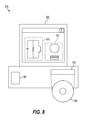
- FIG. 8 is a block diagram illustrating a design workstation used for circuit, layout, and logic design of a semiconductor component according to one configuration.
- Mobile radio frequency (RF) chip designs e.g., mobile RF transceivers
- RF transceivers have migrated to a deep sub-micron process node due to cost and power consumption considerations.
- the design complexity of mobile RF transceivers is further complicated by added circuit functions to support communication enhancements, such as carrier aggregation.
- Further design challenges for mobile RF transceivers include analog/RF performance considerations, including mismatch, noise and other performance considerations.
- the design of these mobile RF transceivers includes the use of passive devices, for example, to suppress resonance, and/or to perform filtering, bypassing and coupling.
- Passive on glass devices involve high performance inductor and capacitor components that have a variety of advantages over other technologies, such as surface mount technology or multi-layer ceramic chips. These advantages include being more compact in size and having smaller manufacturing variations. Passive on glass devices also involve a higher quality (Q)-factor value that meets stringent low insertion loss and low power consumption specifications.
- Devices such as inductors may be implemented as 3D structures with passive on glass technologies. 3D through substrate inductors or other 3D devices may also experience a number of design constraints due to their 3D implementation.
- An inductor is an example of an electrical device used to temporarily store energy in a magnetic field within a wire coil according to an inductance value.
- This inductance value provides a measure of the ratio of voltage to the rate of change of current passing through the inductor.
- inductors are often used in alternating current (AC) electronic equipment, such as radio equipment.
- AC alternating current
- the design of mobile RF transceivers includes the use of inductors with improved inductance density while reducing magnetic loss at high frequency.
- Various aspects of the disclosure provide techniques for fabrication of multiplexers using 2D passive on glass (POG) filters integrated with 3D through glass via (TGV) filters.
- the process flow for semiconductor fabrication of the multiplexer structure may include front-end-of-line (FEOL) processes, middle-of-line (MOL) processes, and back-end-of-line (BEOL) processes.
- FEOL front-end-of-line
- MOL middle-of-line
- BEOL back-end-of-line
- layer includes film and is not to be construed as indicating a vertical or horizontal thickness unless otherwise stated.
- the term “substrate” may refer to a substrate of a diced wafer or may refer to a substrate of a wafer that is not diced.
- the terms chip and die may be used interchangeably unless such interchanging would tax credulity.
- the back-end-of-line interconnect layers may refer to the conductive interconnect layers (e.g., metal one (M 1 ), metal two (M 2 ), metal three (M 3 ), etc.) for electrically coupling to front-end-of-line active devices of an integrated circuit.
- the back-end-of-line interconnect layers may electrically couple to middle-of-line interconnect layers for, for example, connecting M 1 to an oxide diffusion (OD) layer of an integrated circuit.
- a back-end-of-line first via (V 2 ) may connect M 2 to M 3 or others of the back-end-of-line interconnect layers.
- a multiplexer structure includes a high band (HB) filter on a passive substrate.
- the high band filter includes a 2D spiral inductor on the passive substrate.
- the multiplexer structure also includes a low band (LB) filter on the passive substrate.
- the low band filter includes a 3D inductor and a first capacitor on the passive substrate.
- the multiplexer structure further includes at least one through substrate via coupling the high band filter and the low band filter.
- the high band filter and the low band filter are arranged on opposing surfaces of a glass substrate to provide a two-sided multiplexer structure.
- the high band filter includes a second capacitor on a first surface of the passive substrate.
- the high band filter and the low band filter may share the first capacitor on a second surface of the passive substrate opposite the first surface.
- FIG. 1A is a schematic diagram of a radio frequency (RF) front end (RFFE) module 100 employing a diplexer 200 according to an aspect of the present disclosure.
- the RF front end module 100 includes power amplifiers 102 , duplexer/filters 104 , and a radio frequency (RF) switch module 106 .
- the power amplifiers 102 amplify signal(s) to a certain power level for transmission.
- the duplexer/filter 104 filters the input/output signals according to a variety of different parameters, including frequency, insertion loss, rejection or other like parameters.
- the RF switch module 106 may select certain portions of the input signals to pass on to the rest of the RF front end module 100 .
- the RF front end module 100 also includes tuner circuitry 112 (e.g., first tuner circuitry 112 A and second tuner circuitry 112 B), the diplexer 200 , a capacitor 116 , an inductor 118 , a ground terminal 115 and an antenna 114 .
- the tuner circuitry 112 (e.g., the first tuner circuitry 112 A and the second tuner circuitry 112 B) includes components such as a tuner, a portable data entry terminal (PDET), and a house keeping analog to digital converter (HKADC).
- the tuner circuitry 112 may perform impedance tuning (e.g., a voltage standing wave ratio (VSWR) optimization) for the antenna 114 .
- impedance tuning e.g., a voltage standing wave ratio (VSWR) optimization
- the RF front end module 100 also includes a passive combiner 108 coupled to a wireless transceiver (WTR) 120 .
- the passive combiner 108 combines the detected power from the first tuner circuitry 112 A and the second tuner circuitry 112 B.
- the wireless transceiver 120 processes the information from the passive combiner 108 and provides this information to a modem 130 (e.g., a mobile station modem (MSM)).
- MSM mobile station modem
- the modem 130 provides a digital signal to an application processor (AP) 140 .
- AP application processor
- the diplexer 200 is between the tuner component of the tuner circuitry 112 and the capacitor 116 , the inductor 118 , and the antenna 114 .
- the diplexer 200 may be placed between the antenna 114 and the tuner circuitry 112 to provide high system performance from the RF front end module 100 to a chipset including the wireless transceiver 120 , the modem 130 and the application processor 140 .
- the diplexer 200 also performs frequency domain multiplexing on both high band frequencies and low band frequencies.
- the output of the diplexer 200 is fed to an optional LC (inductor/capacitor) network including the capacitor 116 and the inductor 118 .
- the LC network may provide extra impedance matching components for the antenna 114 , when desired. Then a signal with the particular frequency is transmitted or received by the antenna 114 .
- a single capacitor and inductor are shown, multiple components are also contemplated.
- FIG. 1B is a schematic diagram of a WiFi module 170 including a first diplexer 200 - 1 and an RF front end module 150 including a second diplexer 200 - 2 for a chipset 160 to provide carrier aggregation according to an aspect of the present disclosure.
- the WiFi module 170 includes the first diplexer 200 - 1 communicably coupling an antenna 192 to a wireless local area network module (e.g., WLAN module 172 ).
- the RF front end module 150 includes the second diplexer 200 - 2 communicably coupling an antenna 194 to the wireless transceiver (WTR) 120 through a duplexer 180 .
- WTR wireless transceiver
- the wireless transceiver 120 and the WLAN module 172 of the WiFi module 170 are coupled to a modem (MSM, e.g., baseband modem) 130 that is powered by a power supply 152 through a power management integrated circuit (PMIC) 156 .
- the chipset 160 also includes capacitors 162 and 164 , as well as an inductor(s) 166 to provide signal integrity.
- the PMIC 156 , the modem 130 , the wireless transceiver 120 , and the WLAN module 172 each include capacitors (e.g., 158 , 132 , 122 , and 174 ) and operate according to a clock 154 .
- the geometry and arrangement of the various inductor and capacitor components in the chipset 160 may reduce the electromagnetic coupling between the components.
- FIG. 2A is a schematic diagram of a diplexer 200 according to an aspect of the present disclosure.
- the diplexer 200 includes a high band (HB) input port 202 , a low band (LB) input port 204 , and an antenna 206 .
- a high band path of the diplexer 200 includes an input capacitor 218 (C 5 ) and a first parallel coupled capacitor 242 (C 2 ) with a fourth inductor 240 (L 4 ).
- the high band path also includes a second capacitor 216 (C 4 ) and a second parallel coupled capacitor 232 (C 3 ) with a third inductor 230 (L 3 ), and an output capacitor 228 (C 1 ).
- a low band path of the diplexer 200 includes an input capacitor 214 (C 6 ) and a first parallel coupled capacitor 222 (C 7 ) with a second inductor 220 (L 2 ).
- the low band path also includes a second capacitor 212 (C 8 ) and a first inductor 210 (L 1 ). Operation of the diplexer 200 is controlled by the first inductor 210 , the second inductor 220 , the third inductor 230 , and the fourth inductor 240 , as shown in the graph 250 of FIG. 2B .
- FIG. 2B is a graph 250 illustrating performance of a diplexer design according to an aspect of the present disclosure.
- the x-axis of the graph 250 reflects the frequency in gigahertz (GHz) and the y-axis of the graph 250 reflects a decibel (dB) rating.
- a high pass filter curve 252 is a frequency response (transmission in dB) of the third inductor 230 (L 3 ) and the fourth inductor 240 (L 4 ).
- a low pass filter curve 254 is a frequency response (transmission in dB) of the first inductor 210 (L 1 ) and the second inductor 220 (L 2 ).
- GHz gigahertz
- dB decibel
- a high pass filter curve 252 is a frequency response (transmission in dB) of the third inductor 230 (L 3 ) and the fourth inductor 240 (L 4 ).
- a low pass filter curve 254 is a frequency response (transmission in d
- an antenna pad (e.g., the antenna 206 ) is the output for both the high band path and the low band path, whereas the input ports (e.g., the high band input port 202 and the low band input port 204 ) are separate.
- meeting the low pass filter curve 254 may involve higher performance inductors (e.g., the first inductor 210 (L 1 ) and the second inductor 220 (L 2 )) than the inductors (e.g., the third inductor 230 (L 3 ) and the fourth inductor 240 (L 4 )) for meeting the high pass filter curve 252 .
- FIG. 2C is a diagram further illustrating the diplexer 200 of FIG. 2A according to an aspect of the present disclosure.
- the diplexer 200 includes a high band (HB) input port 202 , a low band (LB) input port 204 , and an antenna 206 coupled to an output port.
- a high band path of the diplexer 200 includes a high band antenna switch 260 - 1 .
- a low band path of the diplexer 200 includes a low band antenna switch 260 - 2 .
- a wireless device including an RF front end module may use the antenna switches 260 and the diplexer 200 to enable a wide range band for an RF input and an RF output of the wireless device.
- the antenna 206 may be a multiple input, multiple output (MIMO) antenna. Multiple input, multiple output antennas will be widely used for the RF front end of wireless devices to support features such as carrier aggregation.
- MIMO multiple input, multiple output antennas
- FIG. 3A is a top view of a layout of a diplexer design 300 according to an aspect of the present disclosure.
- the layout of the diplexer design 300 corresponds to the schematic diagram of the diplexer 200 from FIG. 2A according to a 2D configuration.
- the components are implemented in (or on) a passive substrate 308 .
- the term “passive substrate” may refer to a substrate of a diced wafer or panel, or may refer to the substrate of a wafer/panel that is not diced.
- the passive substrate is comprised of glass, air, quartz, sapphire, high-resistivity silicon, or other like passive material.
- the passive substrate may be a coreless substrate.
- the diplexer design 300 includes a high band (HB) input path 302 , a low band (LB) input path 304 , and an antenna 306 .
- the first inductor 310 (L 1 ) and the second inductor 320 (L 2 ) are arranged using 2D spiral inductors.
- the third inductor 330 and the fourth inductor 340 are also arranged using 2D spiral inductors.
- the various capacitor (e.g., C 1 to C 8 ) are also shown and arranged according to the configuration shown in FIG. 2A .
- a thickness of the 2D planar inductors may be within a range of ten (10) to thirty (30) micrometers.
- the footprint occupied by the diplexer design 300 may be in the range of 2 micrometers by 2.5 micrometers due to the 2D planar spiral configuration of the inductors. While this arrangement may be fabricated using less complicated designs, this arrangement consumes additional space.
- FIG. 3B shows a cross section view 350 of the diplexer design 300 of FIG. 3A according to aspects of the present disclosure. For purposes of illustration, only the first inductor 310 (L 1 ) and the second inductor 320 (L 2 ) are shown, as supported by a passive substrate 308 .
- FIG. 4A is a top view of a layout of a diplexer design 400 according to an aspect of the present disclosure.
- the layout of the diplexer design 400 corresponds to the schematic diagram of the diplexer 200 from FIG. 2A according to a 3D implementation.
- the components are implemented in (or on) a passive substrate 408 (see FIG. 4B ), comprised of glass, air, quartz, sapphire, high-resistivity silicon, or other like passive material.
- the diplexer design 400 also includes a high band (HB) input path 402 , a low band (LB) input path 404 , and an antenna 406 .
- the first inductor 410 (L 1 ) and the second inductor 420 (L 2 ) are arranged using 3D spiral inductors.
- the third inductor 430 and the fourth inductor 440 are also arranged using 3D spiral inductors.
- the various capacitor e.g., C 1 to C 8
- a reduced footprint is occupied by the diplexer design 400 , which is in the range of 2 millimeters by 1.7 millimeters, relative to the diplexer design 300 of FIGS. 3A and 3B .
- FIG. 4B shows a cross section view 450 of the diplexer design 400 of FIG. 4A according to aspects of the present disclosure.
- first inductor 410 L 1
- second inductor 420 L 2
- the structures of the various inductors and capacitors shown in FIGS. 3A to 4B are not limited to the structures shown and can take on any structure, such that the layout of the diplexer designs 300 / 400 are possible implementations of the diplexer 200 shown in FIG. 2A .
- the geometry and arrangement of the various inductor and capacitor components in the diplexer 200 may be configured to further reduce the electromagnetic coupling between the components.
- the inductors e.g., the first inductor 410 (L 1 ), the second inductor 420 (L 2 ), the third inductor 430 (L 3 ), and the fourth inductor 440 (L 4 )
- the inductors are high performance inductors implemented in a 3D configuration as a series of traces and through substrate vias that are further illustrated in the cross section view of FIG. 4B .
- the diplexer design 400 of FIGS. 4A and 4B occupies a smaller footprint than the diplexer design 300 of FIGS. 3A and 3B
- fabrication of the diplexer design 400 is more complex and involves additional cost to implement the high performance 3D inductors (e.g., 410 , 420 , 430 , and 440 ).
- the dual-sided printing process enables the printing of conductive interconnect layers (e.g., metal A (MA), metal B (MB), metal C (MC), etc.) on a first surface 509 - 1 of the passive substrate 508 .
- This dual-sided printing process also enables the printing of back-end-of-line (BEOL) interconnect layers (e.g., metal 1 (M 1 ), metal 2 (M 2 ), metal 3 (M 3 ), etc.) on a second surface 509 - 2 of the passive substrate 508 .
- BEOL back-end-of-line
- this dual-sided printing process enables a two-sided multiplexer structure, as described in further detail below.
- the high band filter includes 2D spiral inductor(s) (e.g., the third inductor 530 (L 3 ) and the fourth inductor 540 (L 4 )) on the passive substrate 508 .
- the multiplexer structure 500 also includes a low band (LB) filter 504 on the passive substrate 508 .
- the low band filter 504 includes 3D inductor(s) (e.g., the first inductor 510 (L 1 ) and the second inductor 520 (L 2 )) and a first capacitor (C 1 ) on the passive substrate 508 .
- the multiplexer structure 500 further includes a through substrate via(s) (VIA) coupling the high band filter 502 and the low band filter 504 .
- VIP through substrate via(s)
- the high band filter 502 and the low band filter 504 are arranged on opposing surfaces of a glass substrate panel to provide a two-sided multiplexer structure.
- the high band filter 502 includes a second capacitor (C 2 ) on a first surface 509 - 1 of the passive substrate 508 .
- the high band filter 502 and the low band filter 504 may share the first capacitor C 1 on a second surface 509 - 2 of the passive substrate 508 opposite the first surface 509 - 1 .
- the first surface of the passive substrate is a back-side of the two-sided multiplexer distal from a system board (e.g., a printed circuit board (PCB)).
- PCB printed circuit board
- the first capacitor C 1 is formed from back-end-of-line (BEOL) interconnect layers M 1 and M 2 , separated by a dielectric layer (e.g., aluminum oxide) on the second surface 509 - 2 of the passive substrate 508 .
- BEOL back-end-of-line
- the first capacitor C 1 is coupled to BEOL interconnect layer M 3 through a through substrate via V 2 .
- the second capacitor C 2 is formed from conductive interconnect layers MA and MB separated by a dielectric on the first surface 509 - 1 of the passive substrate 508 .
- the third inductor 530 (L 3 ) and the fourth inductor 540 (L 4 ) may be formed from conductive interconnect layer MC, whereas the first inductor 510 (L 1 ) and the second inductor 520 (L 2 ) may be formed from BEOL interconnect layer M 1 .
- the multiplexer structure 500 is also surrounded by a final passivation layer VP (e.g., polyimide or solder resist).
- VP e.g., polyimide or solder resist
- side A of the multiplexer structure 500 also includes the low band filter 504 including the first inductor 510 (L 1 ) and the second inductor 520 (L 2 )) arranged as 3D inductors within a 1 millimeter by 1.7 millimeter footprint.
- the multiplexer structure 500 further includes a through substrate via(s) (VIA) coupling the high band filter 502 and the low band filter 504 .
- FIG. 6 is a process flow diagram illustrating a method 600 of constructing a multiplexer structure according to an aspect of the present disclosure.
- a high band (HB) filter including a 2D planar spiral inductor
- the multiplexer structure 500 includes the high band filter 502 on the first surface 509 - 1 of the passive substrate 508 .
- the high band filter may include 2D planar spiral inductor(s) (e.g., the third inductor 530 (L 3 ) and the fourth inductor 540 (L 4 )) on the first surface 509 - 1 of the passive substrate 508 .
- the passive substrate 508 may be formed by dicing a glass substrate panel along the dicing lines, which may be referred to herein as “dicing streets.”
- the dicing lines indicate where the glass panel substrate is to be broken apart or separated into pieces.
- the dicing lines may define the outline of the various RF circuits that have been fabricated on the glass panel substrate. This dicing process may be performed using a stealth dicing process that involves a scribing and cracking process along the dicing street without material loss. Stealth dicing may be distinguished from the dicing of silicon, which involves material loss due to grinding of, for example, a saw blade along the dicing street.
- a low band (LB) filter including a 3D through-substrate inductor and a first capacitor, is fabricated on the passive substrate panel.
- the multiplexer structure 500 includes the low band filter 504 on the second surface 509 - 2 of the passive substrate 508 .
- the low band filter may include 3D through-substrate inductor(s) (e.g., the first inductor 510 (L 1 ) and the second inductor 520 (L 2 )) and a first capacitor (C 1 ), on the second surface 509 - 2 of the passive substrate 508 .
- a through substrate via is fabricated through the passive substrate, coupling the high band filter and the low band filter.
- the multiplexer structure 500 further includes a through substrate via(s) (VIA) coupling the high band filter 502 and the low band filter 504 .
- the method 600 may also include fabricating at least one second capacitor on the first surface of the passive substrate.
- a dual-sided printing process for a glass panel substrate enables a two-sided multiplexer structure, for example, as shown in FIG. 5A .
- the method of constructing the multiplexer structure may be performed in any desired order including, but not limited to, performing the method 600 is reverse order beginning with block 606 and terminating with block 602 .
- circuitry for multiplexer structures using through glass via or through substrate via technology includes high band filters and low band filters on opposing surfaces of a passive substrate.
- the multiplexer structure further includes means for coupling the high band filter and the low band filter.
- the coupling means may be the through substrate VIA, shown in FIG. 5A .
- the aforementioned means may be any module or any apparatus configured to perform the functions recited by the aforementioned means.
- a multiplexer structure includes a high band (HB) filter on a passive substrate.
- the high band filter includes a 2D spiral inductor on the passive substrate.
- the multiplexer structure also includes a low band (LB) filter on the passive substrate.
- the low band filter includes a 3D inductor and a first capacitor on the passive substrate.
- the multiplexer structure further includes at least one through substrate via coupling the high band filter and the low band filter.
- the high band filter and the low band filter are arranged on opposing surfaces of a glass substrate to provide a two-sided multiplexer structure.
- the high band filter includes a second capacitor on a first surface of the passive substrate.
- the high band filter and the low band filter may share the first capacitor on a second surface of the passive substrate opposite the first surface.
- the first inductor 410 and the second inductor 420 may be implemented using the higher cost 3D arrangement shown in FIGS. 4A and 4B .
- the higher performance inductors may be high-Q, high-density 3D inductors for critical bands (e.g., the low band).
- the third inductor 330 (L 3 ) and the fourth inductor 340 (L 4 ) may be implemented using the lower cost and simplified 2D planar arrangement shown in FIGS. 3A and 3B .
- placing the 2D filters away from the system board (e.g., PCB) may eliminate customer specific ground plan impact.
- FIG. 7 is a block diagram showing an exemplary wireless communication system 700 in which an aspect of the disclosure may be advantageously employed.
- FIG. 7 shows three remote units 720 , 730 , and 750 and two base stations 740 .
- Remote units 720 , 730 , and 750 include IC devices 725 A, 725 C, and 725 B that include the disclosed multiplexer structures. It will be recognized that other devices may also include the disclosed multiplexer devices, such as the base stations, switching devices, and network equipment.
- FIG. 7 shows forward link signals 780 from the base station 740 to the remote units 720 , 730 , and 750 and reverse link signals 790 from the remote units 720 , 730 , and 750 to base stations 740 .
- remote unit 720 is shown as a mobile telephone
- remote unit 730 is shown as a portable computer
- remote unit 750 is shown as a fixed location remote unit in a wireless local loop system.
- a remote units may be a mobile phone, a hand-held personal communication systems (PCS) unit, a portable data unit such as a personal digital assistant (PDA), a GPS enabled device, a navigation device, a set top box, a music player, a video player, an entertainment unit, a fixed location data unit such as a meter reading equipment, or other communications device that stores or retrieve data or computer instructions, or combinations thereof.
- FIG. 7 illustrates remote units according to the aspects of the disclosure, the disclosure is not limited to these exemplary illustrated units. Aspects of the disclosure may be suitably employed in many devices, which include the disclosed multiplexer devices.
- FIG. 8 is a block diagram illustrating a design workstation used for circuit, layout, and logic design of a semiconductor component, such as the multiplexer devices disclosed above.
- a design workstation 800 includes a hard disk 801 containing operating system software, support files, and design software such as Cadence or OrCAD.
- the design workstation 800 also includes a display 802 to facilitate design of a circuit 810 or a semiconductor component 812 such as a multiplexer device.
- a storage medium 804 is provided for tangibly storing the circuit design 810 or the semiconductor component 812 .
- the circuit design 810 or the semiconductor component 812 may be stored on the storage medium 804 in a file format such as GDSII or GERBER.
- the storage medium 804 may be a CD-ROM, DVD, hard disk, flash memory, or other appropriate device.
- the design workstation 800 includes a drive apparatus 803 for accepting input from or writing output to the storage medium 804 .
- Data recorded on the storage medium 804 may specify logic circuit configurations, pattern data for photolithography masks, or mask pattern data for serial write tools such as electron beam lithography.
- the data may further include logic verification data such as timing diagrams or net circuits associated with logic simulations.
- Providing data on the storage medium 804 facilitates the design of the circuit design 810 or the semiconductor component 812 by decreasing the number of processes for designing semiconductor wafers.
- the functions may be stored as one or more instructions or code on a computer-readable medium. Examples include computer-readable media encoded with a data structure and computer-readable media encoded with a computer program.
- Computer-readable media includes physical computer storage media. A storage medium may be an available medium that can be accessed by a computer.
- such computer-readable media can include RAM, ROM, EEPROM, CD-ROM or other optical disk storage, magnetic disk storage or other magnetic storage devices, or other medium that can be used to store desired program code in the form of instructions or data structures and that can be accessed by a computer; disk and disc, as used herein, includes compact disc (CD), laser disc, optical disc, digital versatile disc (DVD), floppy disk and Blu-ray disc where disks usually reproduce data magnetically, while discs reproduce data optically with lasers. Combinations of the above should also be included within the scope of computer-readable media.
- instructions and/or data may be provided as signals on transmission media included in a communication apparatus.
- a communication apparatus may include a transceiver having signals indicative of instructions and data. The instructions and data are configured to cause one or more processors to implement the functions outlined in the claims.
Landscapes
- Engineering & Computer Science (AREA)
- Power Engineering (AREA)
- Filters And Equalizers (AREA)
- Transceivers (AREA)
- Coils Or Transformers For Communication (AREA)
- Manufacturing & Machinery (AREA)
Priority Applications (9)
| Application Number | Priority Date | Filing Date | Title |
|---|---|---|---|
| US15/067,106 US9954267B2 (en) | 2015-12-28 | 2016-03-10 | Multiplexer design using a 2D passive on glass filter integrated with a 3D through glass via filter |
| JP2018531145A JP2019507972A (ja) | 2015-12-28 | 2016-12-05 | 3dガラス貫通ビアフィルタと統合された2d受動オンガラスフィルタを使用するマルチプレクサ構成 |
| PCT/US2016/064962 WO2017116616A1 (en) | 2015-12-28 | 2016-12-05 | Multiplexer design using a 2d passive on glass filter integrated with a 3d through glass via filter |
| CA3004764A CA3004764C (en) | 2015-12-28 | 2016-12-05 | Multiplexer design using a 2d passive on glass filter integrated with a 3d through glass via filter |
| CN201680076967.5A CN108476014A (zh) | 2015-12-28 | 2016-12-05 | 使用与3d贯穿玻璃通孔滤波器集成的2d无源玻璃滤波器的多路复用器设计 |
| KR1020187016158A KR102093160B1 (ko) | 2015-12-28 | 2016-12-05 | 3d 글래스 관통 비아 필터와 통합되는 2d 패시브 온 글래스 필터를 사용하는 멀티플렉서 설계 |
| EP16816120.6A EP3378160B1 (en) | 2015-12-28 | 2016-12-05 | Multiplexer design using a 2d passive on glass filter integrated with a 3d through glass via filter |
| BR112018012738A BR112018012738A2 (pt) | 2015-12-28 | 2016-12-05 | projeto multiplexador usando um filtro em vidro passivo 2d integrado com um filtro via vidro direto 3d |
| TW105140297A TWI639316B (zh) | 2015-12-28 | 2016-12-06 | 使用整合2d被動玻璃上濾波器及3d貫通玻璃通孔濾波器之多工器設計 |
Applications Claiming Priority (2)
| Application Number | Priority Date | Filing Date | Title |
|---|---|---|---|
| US201562271893P | 2015-12-28 | 2015-12-28 | |
| US15/067,106 US9954267B2 (en) | 2015-12-28 | 2016-03-10 | Multiplexer design using a 2D passive on glass filter integrated with a 3D through glass via filter |
Publications (2)
| Publication Number | Publication Date |
|---|---|
| US20170187345A1 US20170187345A1 (en) | 2017-06-29 |
| US9954267B2 true US9954267B2 (en) | 2018-04-24 |
Family
ID=59088028
Family Applications (1)
| Application Number | Title | Priority Date | Filing Date |
|---|---|---|---|
| US15/067,106 Active 2036-04-28 US9954267B2 (en) | 2015-12-28 | 2016-03-10 | Multiplexer design using a 2D passive on glass filter integrated with a 3D through glass via filter |
Country Status (9)
Cited By (4)
| Publication number | Priority date | Publication date | Assignee | Title |
|---|---|---|---|---|
| US20190035621A1 (en) * | 2017-07-25 | 2019-01-31 | Qualcomm Incorporated | Shaped circuit wafers |
| US10944379B2 (en) * | 2016-12-14 | 2021-03-09 | Qualcomm Incorporated | Hybrid passive-on-glass (POG) acoustic filter |
| US11296670B2 (en) | 2020-01-23 | 2022-04-05 | Qualcomm Incorporated | Impedance matching transceiver |
| US11406025B2 (en) * | 2017-12-11 | 2022-08-02 | Toppan Printing Co., Ltd. | Glass wiring board, method for manufacturing the same, and semiconductor device |
Families Citing this family (20)
| Publication number | Priority date | Publication date | Assignee | Title |
|---|---|---|---|---|
| US10043136B1 (en) * | 2017-10-12 | 2018-08-07 | International Business Machines Corporation | Reducing the number of input lines to superconducting quantum processors installed inside dilution refrigerators |
| US10582609B2 (en) | 2017-10-30 | 2020-03-03 | Qualcomm Incorporated | Integration of through glass via (TGV) filter and acoustic filter |
| TWI678952B (zh) | 2017-12-13 | 2019-12-01 | 欣興電子股份有限公司 | 線路板結構及其製作方法 |
| TWI669997B (zh) * | 2018-01-25 | 2019-08-21 | 欣興電子股份有限公司 | 線路板結構及其製作方法 |
| WO2019225698A1 (ja) * | 2018-05-24 | 2019-11-28 | 凸版印刷株式会社 | 回路基板 |
| US10840884B2 (en) | 2018-05-24 | 2020-11-17 | Qualcomm Incorporated | Bulk acoustic wave (BAW) and passive-on-glass (POG) filter co-integration |
| US11190160B2 (en) * | 2018-11-16 | 2021-11-30 | Anhui Anuki Technologies Co., Ltd. | Frequency multiplexer |
| US10879169B2 (en) * | 2018-12-26 | 2020-12-29 | Qualcomm Incorporated | Integrated inductors for power management circuits |
| US11121699B2 (en) | 2019-02-19 | 2021-09-14 | Qualcomm Incorporated | Wideband filter with resonators and inductors |
| EP3989440A4 (en) * | 2019-06-18 | 2022-08-10 | Toppan Inc. | MULTILAYER WIRING BOARD HAVING LC RESONANT CIRCUIT, AND ELECTRONIC COMPONENT BOX USING MULTILAYER WIRING BOARD HAVING LC RESONANT CIRCUIT |
| JP7512594B2 (ja) * | 2020-01-10 | 2024-07-09 | Toppanホールディングス株式会社 | 回路基板 |
| TWI780668B (zh) * | 2020-05-28 | 2022-10-11 | 日商村田製作所股份有限公司 | 用於半導體複合裝置之模組 |
| US11652468B2 (en) * | 2020-07-07 | 2023-05-16 | Qualcomm Incorporated | High performance tunable filter |
| CN112511126B (zh) * | 2020-10-30 | 2022-03-15 | 诺思(天津)微系统有限责任公司 | 多工器和改善多工器隔离度的方法以及通信设备 |
| CN116420201A (zh) | 2020-11-06 | 2023-07-11 | 株式会社村田制作所 | 滤波器装置以及搭载有该滤波器装置的高频前端电路 |
| WO2022222124A1 (zh) * | 2021-04-23 | 2022-10-27 | 京东方科技集团股份有限公司 | 集成有无源器件的基板及其制备方法 |
| JP7712828B2 (ja) * | 2021-09-14 | 2025-07-24 | Tdk株式会社 | 積層型電子部品 |
| JP2025507799A (ja) * | 2022-03-17 | 2025-03-21 | ノースロップ グラマン システムズ コーポレーション | 音響共振器フィルタバンクシステム |
| US20250096763A1 (en) * | 2022-08-25 | 2025-03-20 | Boe Technology Group Co., Ltd. | Filter, Manufacturing Method Therefor and Electronic Device |
| US20240429587A1 (en) * | 2023-06-22 | 2024-12-26 | Qualcomm Incorporated | Low emission three-dimensional frequency multiplexer |
Citations (9)
| Publication number | Priority date | Publication date | Assignee | Title |
|---|---|---|---|---|
| US6646534B2 (en) * | 1999-07-09 | 2003-11-11 | Micron Technology, Inc. | Integrated circuit inductors |
| US7135943B2 (en) * | 2004-07-11 | 2006-11-14 | Chi Mei Communication Sytems, Inc. | Diplexer formed in multi-layered substrate |
| US20130271239A1 (en) | 2012-04-13 | 2013-10-17 | Yu-Lin Liao | Diplexer |
| US8736399B2 (en) | 2011-04-06 | 2014-05-27 | M/A-Com Technology Solutions Holdings, Inc. | Triplexer topology |
| US20140197902A1 (en) | 2013-01-11 | 2014-07-17 | Qualcomm Incorporated | Diplexer design using through glass via technology |
| US20140268616A1 (en) | 2013-03-15 | 2014-09-18 | Qualcomm Incorporated | Capacitor with a dielectric between a via and a plate of the capacitor |
| US20140354378A1 (en) | 2013-05-31 | 2014-12-04 | Qualcomm Incorporated | Design for high pass filters and low pass filters using through glass via technology |
| US20140354372A1 (en) | 2013-06-04 | 2014-12-04 | Qualcomm Incorporated | Systems for reducing magnetic coupling in integrated circuits (ics), and related components and methods |
| US20150304059A1 (en) | 2014-04-18 | 2015-10-22 | Qualcomm Incorporated | Frequency multiplexer |
Family Cites Families (12)
| Publication number | Priority date | Publication date | Assignee | Title |
|---|---|---|---|---|
| JP3939192B2 (ja) * | 2002-04-24 | 2007-07-04 | 三洋電機株式会社 | 分波器 |
| JP2004072582A (ja) * | 2002-08-08 | 2004-03-04 | Matsushita Electric Ind Co Ltd | 高周波デバイス |
| JP4423210B2 (ja) * | 2005-01-21 | 2010-03-03 | 京セラ株式会社 | 高周波モジュール及びそれを用いた通信機器 |
| EP2352226A4 (en) * | 2008-10-24 | 2013-12-04 | Murata Manufacturing Co | ELECTRONIC COMPONENT AND METHOD FOR PRODUCING AN ELECTRONIC COMPONENT |
| US9048112B2 (en) * | 2010-06-29 | 2015-06-02 | Qualcomm Incorporated | Integrated voltage regulator with embedded passive device(s) for a stacked IC |
| US20120190152A1 (en) * | 2011-01-25 | 2012-07-26 | Taiwan Semiconductor Manufacturing Company, Ltd. | Methods for Fabricating Integrated Passive Devices on Glass Substrates |
| US8803615B2 (en) * | 2012-01-23 | 2014-08-12 | Qualcomm Incorporated | Impedance matching circuit with tunable notch filters for power amplifier |
| US8666338B2 (en) * | 2012-01-23 | 2014-03-04 | Qualcomm Incorporated | Multi-mode bypass driver amplifier with tunable load matching |
| US9331720B2 (en) * | 2012-01-30 | 2016-05-03 | Qualcomm Incorporated | Combined directional coupler and impedance matching circuit |
| CN103490793B (zh) * | 2012-06-12 | 2015-08-19 | 太阳诱电株式会社 | 高频电路模块 |
| JP6409255B2 (ja) * | 2013-07-31 | 2018-10-24 | 株式会社村田製作所 | デュプレクサ |
| US9847804B2 (en) * | 2014-04-30 | 2017-12-19 | Skyworks Solutions, Inc. | Bypass path loss reduction |
-
2016
- 2016-03-10 US US15/067,106 patent/US9954267B2/en active Active
- 2016-12-05 BR BR112018012738A patent/BR112018012738A2/pt not_active Application Discontinuation
- 2016-12-05 JP JP2018531145A patent/JP2019507972A/ja active Pending
- 2016-12-05 CN CN201680076967.5A patent/CN108476014A/zh active Pending
- 2016-12-05 WO PCT/US2016/064962 patent/WO2017116616A1/en active Application Filing
- 2016-12-05 CA CA3004764A patent/CA3004764C/en active Active
- 2016-12-05 EP EP16816120.6A patent/EP3378160B1/en not_active Not-in-force
- 2016-12-05 KR KR1020187016158A patent/KR102093160B1/ko active Active
- 2016-12-06 TW TW105140297A patent/TWI639316B/zh not_active IP Right Cessation
Patent Citations (10)
| Publication number | Priority date | Publication date | Assignee | Title |
|---|---|---|---|---|
| US6646534B2 (en) * | 1999-07-09 | 2003-11-11 | Micron Technology, Inc. | Integrated circuit inductors |
| US7135943B2 (en) * | 2004-07-11 | 2006-11-14 | Chi Mei Communication Sytems, Inc. | Diplexer formed in multi-layered substrate |
| US8736399B2 (en) | 2011-04-06 | 2014-05-27 | M/A-Com Technology Solutions Holdings, Inc. | Triplexer topology |
| US20130271239A1 (en) | 2012-04-13 | 2013-10-17 | Yu-Lin Liao | Diplexer |
| US20140197902A1 (en) | 2013-01-11 | 2014-07-17 | Qualcomm Incorporated | Diplexer design using through glass via technology |
| US9203373B2 (en) | 2013-01-11 | 2015-12-01 | Qualcomm Incorporated | Diplexer design using through glass via technology |
| US20140268616A1 (en) | 2013-03-15 | 2014-09-18 | Qualcomm Incorporated | Capacitor with a dielectric between a via and a plate of the capacitor |
| US20140354378A1 (en) | 2013-05-31 | 2014-12-04 | Qualcomm Incorporated | Design for high pass filters and low pass filters using through glass via technology |
| US20140354372A1 (en) | 2013-06-04 | 2014-12-04 | Qualcomm Incorporated | Systems for reducing magnetic coupling in integrated circuits (ics), and related components and methods |
| US20150304059A1 (en) | 2014-04-18 | 2015-10-22 | Qualcomm Incorporated | Frequency multiplexer |
Non-Patent Citations (5)
| Title |
|---|
| International Search Report and Written Opinion—PCT/US2016/064962—ISA/EPO—dated Mar. 10, 2017. |
| KAI LIU ; ROBERT FRYE ; MAPHOOPWINT HLAING ; YONGTAEK LEE ; HYUNTAI KIM ; GWANG KIM ; BILLY AHN: "Investigation of integrated passive device with through-silicon via", ELECTRONIC COMPONENTS AND TECHNOLOGY CONFERENCE (ECTC), 2012 IEEE 62ND, IEEE, 29 May 2012 (2012-05-29), pages 1833 - 1839, XP032210840, ISBN: 978-1-4673-1966-9, DOI: 10.1109/ECTC.2012.6249087 |
| Kumagai M., et al., "Advanced Dicing Technology for Semiconductor Wafer-Stealth Dicing", IEEE Transactions on Semiconductor Manufacturing, IEEE Service Center, Piscataway, NJ, US, vol. 20, No. 3, Aug. 1, 2007 (Aug. 1, 2007), XP011189520, pp. 259-265. |
| Liu K., et al., "Investigation of Integrated Passive Device With Through-silicon Via", Electronic Components and Technology Conference (ECTC), 2012 IEEE 62nd, IEEE, May 29, 2012 (May 29, 2012), pp. 1833-1839, XP032210840, DOI: 10.1109/ECTC.2012.6249087, ISBN: 978-1-4673-1966-9. |
| M. KUMAGAI ; N. UCHIYAMA ; E. OHMURA ; R. SUGIURA ; K. ATSUMI ; K. FUKUMITSU: "Advanced Dicing Technology for Semiconductor Wafer—Stealth Dicing", IEEE TRANSACTIONS ON SEMICONDUCTOR MANUFACTURING., IEEE SERVICE CENTER, PISCATAWAY, NJ., US, vol. 20, no. 3, 1 August 2007 (2007-08-01), US, pages 259 - 265, XP011189520, ISSN: 0894-6507, DOI: 10.1109/TSM.2007.901849 |
Cited By (4)
| Publication number | Priority date | Publication date | Assignee | Title |
|---|---|---|---|---|
| US10944379B2 (en) * | 2016-12-14 | 2021-03-09 | Qualcomm Incorporated | Hybrid passive-on-glass (POG) acoustic filter |
| US20190035621A1 (en) * | 2017-07-25 | 2019-01-31 | Qualcomm Incorporated | Shaped circuit wafers |
| US11406025B2 (en) * | 2017-12-11 | 2022-08-02 | Toppan Printing Co., Ltd. | Glass wiring board, method for manufacturing the same, and semiconductor device |
| US11296670B2 (en) | 2020-01-23 | 2022-04-05 | Qualcomm Incorporated | Impedance matching transceiver |
Also Published As
| Publication number | Publication date |
|---|---|
| EP3378160B1 (en) | 2019-04-24 |
| TWI639316B (zh) | 2018-10-21 |
| BR112018012738A2 (pt) | 2018-12-04 |
| CA3004764C (en) | 2021-01-26 |
| KR102093160B1 (ko) | 2020-03-25 |
| CN108476014A (zh) | 2018-08-31 |
| JP2019507972A (ja) | 2019-03-22 |
| WO2017116616A1 (en) | 2017-07-06 |
| EP3378160A1 (en) | 2018-09-26 |
| CA3004764A1 (en) | 2017-07-06 |
| TW201733280A (zh) | 2017-09-16 |
| KR20180097539A (ko) | 2018-08-31 |
| US20170187345A1 (en) | 2017-06-29 |
Similar Documents
| Publication | Publication Date | Title |
|---|---|---|
| US9954267B2 (en) | Multiplexer design using a 2D passive on glass filter integrated with a 3D through glass via filter | |
| US10256863B2 (en) | Monolithic integration of antenna switch and diplexer | |
| US9876513B2 (en) | LC filter layer stacking by layer transfer to make 3D multiplexer structures | |
| US9203373B2 (en) | Diplexer design using through glass via technology | |
| US10103135B2 (en) | Backside ground plane for integrated circuit | |
| US10840884B2 (en) | Bulk acoustic wave (BAW) and passive-on-glass (POG) filter co-integration | |
| EP3501244B1 (en) | Multi-density mim capacitor for improved passive on glass (pog) multiplexer performance | |
| US10433425B1 (en) | Three-dimensional high quality passive structure with conductive pillar technology | |
| KR102760882B1 (ko) | 개방―패시베이션 볼 그리드 어레이 패드들 | |
| US9780048B1 (en) | Side-assembled passive devices | |
| US11239158B1 (en) | Wire bond inductor structures for flip chip dies | |
| US20170372975A1 (en) | Inline kerf probing of passive devices |
Legal Events
| Date | Code | Title | Description |
|---|---|---|---|
| AS | Assignment |
Owner name: QUALCOMM INCORPORATED, CALIFORNIA Free format text: ASSIGNMENT OF ASSIGNORS INTEREST;ASSIGNORS:YUN, CHANGHAN HOBIE;KIM, DAEIK DANIEL;VELEZ, MARIO FRANCISCO;AND OTHERS;SIGNING DATES FROM 20160620 TO 20160623;REEL/FRAME:039022/0053 |
|
| STCF | Information on status: patent grant |
Free format text: PATENTED CASE |
|
| MAFP | Maintenance fee payment |
Free format text: PAYMENT OF MAINTENANCE FEE, 4TH YEAR, LARGE ENTITY (ORIGINAL EVENT CODE: M1551); ENTITY STATUS OF PATENT OWNER: LARGE ENTITY Year of fee payment: 4 |