US9864446B2 - Touch screen-integrated display device - Google Patents
Touch screen-integrated display device Download PDFInfo
- Publication number
- US9864446B2 US9864446B2 US14/749,322 US201514749322A US9864446B2 US 9864446 B2 US9864446 B2 US 9864446B2 US 201514749322 A US201514749322 A US 201514749322A US 9864446 B2 US9864446 B2 US 9864446B2
- Authority
- US
- United States
- Prior art keywords
- touch
- pad
- circuit board
- printed circuit
- flexible member
- Prior art date
- Legal status (The legal status is an assumption and is not a legal conclusion. Google has not performed a legal analysis and makes no representation as to the accuracy of the status listed.)
- Active, expires
Links
Images


Classifications
-
- G—PHYSICS
- G06—COMPUTING; CALCULATING OR COUNTING
- G06F—ELECTRIC DIGITAL DATA PROCESSING
- G06F3/00—Input arrangements for transferring data to be processed into a form capable of being handled by the computer; Output arrangements for transferring data from processing unit to output unit, e.g. interface arrangements
- G06F3/01—Input arrangements or combined input and output arrangements for interaction between user and computer
- G06F3/03—Arrangements for converting the position or the displacement of a member into a coded form
- G06F3/041—Digitisers, e.g. for touch screens or touch pads, characterised by the transducing means
- G06F3/0412—Digitisers structurally integrated in a display
-
- G—PHYSICS
- G06—COMPUTING; CALCULATING OR COUNTING
- G06F—ELECTRIC DIGITAL DATA PROCESSING
- G06F3/00—Input arrangements for transferring data to be processed into a form capable of being handled by the computer; Output arrangements for transferring data from processing unit to output unit, e.g. interface arrangements
- G06F3/01—Input arrangements or combined input and output arrangements for interaction between user and computer
- G06F3/03—Arrangements for converting the position or the displacement of a member into a coded form
- G06F3/041—Digitisers, e.g. for touch screens or touch pads, characterised by the transducing means
- G06F3/0416—Control or interface arrangements specially adapted for digitisers
- G06F3/04164—Connections between sensors and controllers, e.g. routing lines between electrodes and connection pads
Definitions
- the present invention relates to a touch screen-integrated display device. More particularly, the present invention relates to a touch screen-integrated display device in which a flexible printed circuit board is connected with an entirety of a first pad connected with a display device and a second pad connected with a touch sensing device.
- a touch screen panel is a device configured to sense a user's touch input such as a screen touch or gesture with respect to a display device.
- the touch screen has been widely used for portable display devices such as a smart phone, and a tablet PC and large-sized display devices such as display devices in public facilities and smart TVs.
- a touch screen panel is attached to an upper substrate.
- the touch screen panel is separately manufactured and attached to an external surface of the display device.
- a total thickness of the display device is undesirably large.
- FIG. 1A is a schematic perspective view provided to describe a touch screen-integrated display device of the related art.
- FIG. 1B is a schematic cross-sectional view provided to describe the touch screen-integrated display device taken along a line Ib-Ib′ of FIG. 1A .
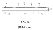
- FIG. 1C is a schematic cross-sectional view provided to describe the touch screen-integrated display device taken along a line Ic-Ic′ of FIG. 1A .
- the touch screen-integrated display device 100 may include a lower substrate 110 , a first pad 111 , a second pad 112 , an upper substrate 120 , a display element 130 , a touch sensing element 140 , a bonding layer 150 , a driver integrated circuit 160 , a first flexible printed circuit board 170 , and a second flexible printed circuit board 190 .
- a first pad area PA 1 and a second pad area PA 2 are disposed in an area of the lower substrate 110 which is not covered by the upper substrate 120 but exposed.
- the first pad area PA 1 the first pad 111 that provides electrical connection with the display element 130 is disposed, whereas in the second pad area PA 2 , the second pad 112 that provides electrical connection with the touch sensing element 140 is disposed.
- An external printed circuit board in which a timing controller, a touch integrated circuit, or the like are disposed, can be connected to the first pad 111 and the second pad 112 via the first flexible printed circuit board 170 and the second flexible printed circuit board 190 .
- the first flexible printed circuit board 170 is used in order to connect the external printed circuit board with the first pad 111 .
- the second flexible printed circuit board 190 is used in order to connect the external printed circuit board with the second pad 112 .
- respective connectors 175 and 195 are used.
- a touch screen panel and a display panel are separate and non-integrated, separate flexible printed circuit boards that are connected with the touch screen panel and the display panel are needed to connect with each of the touch screen panel and the display panel with an external printed circuit board.
- the inventors of the present invention found that if a better structured and designed single flexible printed circuit board is connected to both the first pad and also the second pad of a lower substrate, manufacturing costs for the touch screen-integrated display device can be reduced and the assembly process can be simplified.
- an advantage of the present invention is to provide a touch screen-integrated display device in which a first pad and a second pad can be simply connected with a single external printed circuit board.
- Another advantage of the present invention is to provide a touch screen-integrated display device of which a flexible printed circuit board can be rapidly attached to an external printed circuit board.
- Yet another advantage of the present invention is to provide a touch screen-integrated display device for which manufacturing costs and processing time can be reduced.
- the touch integrated circuit may be disposed on the flexible printed circuit board.
- the present invention has an effect of rapidly and easily connecting an external printed circuit board with pads in an exposure area of a lower substrate.
- the present invention has an effect of reducing costs required for a flexible printed circuit board when a touch screen-integrated display device is manufactured.
- the present invention has an effect of providing a flexible printed circuit board that is suitable for a touch screen-integrated display device.
- FIG. 1A is a schematic perspective view of the related art provided to describe a touch screen-integrated display device
- FIG. 1B is a schematic cross-sectional view of the related art provided to describe the touch screen-integrated display device taken along a line Ib-Ib′ of FIG. 1A ;
- FIG. 1C is a schematic cross-sectional view of the related art provided to describe the touch screen-integrated display device taken along a line Ic-Ic′ of FIG. 1A ;
- FIG. 2A is a schematic perspective view provided to describe a touch screen-integrated display device according to an exemplary embodiment of the present invention
- FIG. 2B is a schematic cross-sectional view provided to describe the touch screen-integrated display device taken along a line IIb-IIb′ of FIG. 2A according to an exemplary embodiment of the present invention
- FIG. 2C is a schematic cross-sectional view provided to describe the touch screen-integrated display device taken along a line IIc-IIc′ of FIG. 2A according to an exemplary embodiment of the present invention
- FIG. 2D is a schematic plane view provided to describe a lower substrate according to an exemplary embodiment of the present invention.
- FIG. 2E is a schematic plane view provided to describe an upper substrate according to an exemplary embodiment of the present invention.
- FIG. 2F provides schematic plane views to describe a flexible printed circuit board according to an exemplary embodiment of the present invention.
- FIG. 3A is a perspective view provided to describe a touch screen-integrated display device according to another exemplary embodiment of the present invention.
- FIG. 3B provides plane views to describe a flexible printed circuit board according to another exemplary embodiment of the present invention.
- FIGS. 4A and 4B provide plane views to describe a touch screen-integrated display device according to another exemplary embodiment of the present invention.
- Components are interpreted to include margins of error or to be within a range of ordinary manufacturing tolerance even if not expressly stated.
- first”, “second”, and the like are used for describing various components, these components are not confined by these terms. These terms are merely used for distinguishing one component from the other components. Therefore, a first component to be mentioned below may be the same or different from a second component depending upon the technical concepts of the present invention.
- FIG. 2A is a schematic perspective view provided to describe a touch screen-integrated display device according to an exemplary embodiment of the present invention.
- FIG. 2B is a schematic cross-sectional view provided to describe the touch screen-integrated display device taken along a line IIb-IIb′ of FIG. 2A according to an exemplary embodiment of the present invention.
- FIG. 2C is a schematic cross-sectional view provided to describe the touch screen-integrated display device taken along a line IIc-IIc′ of FIG. 2A according to an exemplary embodiment of the present invention.
- a touch screen-integrated display device 200 includes a lower substrate 210 , a first pad 211 , a second pad 212 , an upper substrate 220 , a display element 230 , a touch sensing element 240 , a bonding layer 250 , a driver integrated circuit 260 , a flexible printed circuit board (FPCB) 270 , and a touch integrated circuit 280 .
- the lower substrate 210 is configured to accommodate or support various components of the touch screen-integrated display device 200 and can be made of an insulating material such as glass. Also, the lower substrate 210 may be made of a flexible material, for example, plastic such as polyimide. Since the lower substrate 210 is made of a flexible material, a back plate for supporting the lower substrate 210 may be used.
- FIG. 2D is a schematic plane view provided to describe a lower substrate according to an exemplary embodiment of the present invention.
- FIG. 2D illustrates only the first pad 211 , the second pad 212 , a first line 213 , a second line 214 , a lower connecting pad 215 , the display element 230 , and the driver integrated circuit 260 among the components disposed on the lower substrate 210 .
- the lower substrate 210 may include a device area DA and an exposure area EA.
- the device area DA accommodates various components configured to display images, and the display element 230 and the touch sensing element 240 are disposed in the device area DA.
- the exposure area EA extends from one side of the device area DA, and is not covered by the upper substrate 220 . However, the exposure EA is exposed, whereas the lower substrate 210 and the upper substrate 220 are bonded to each other.
- the exposure area EA may include a first pad area PA 1 where the first pad 211 is disposed and a second pad area PA 2 where the second pad 212 is disposed.
- a pad refers to terminals or connectors that allow electrical connections between different components.
- a single first pad area PA 1 and two second pad areas PA 2 may be provided in the single touch screen-integrated display device 200 .
- the two second pad areas PA 2 are disposed on the corners of the lower substrate 210
- the first pad area PA 1 may be disposed between the two second pad areas PA 2 .
- alternative locations and configurations other than those depicted fall within the technical scope of the exemplary embodiments described herein.
- the first pad 211 is disposed in the first pad area PA 1 of the lower substrate 210 .
- the first pad 211 which has a special structure and particular configuration, is electrically connected with the display element 230 through the first line 213 and is also electrically connected with a first pad connecting unit 273 of the flexible printed circuit board 270 .
- the first pad 211 is configured to carry, transfer, or otherwise used to transmit signals for displaying an image to the display element 230 .
- the first pad 211 may be made of a highly conductive material such as metals including aluminum (Al), aluminum (Al) alloys, copper (Cu), copper (Cu) alloys, molybdenum (Mo), and chromium (Cr).
- the second pad 212 which has a special structure and particular configuration, is disposed in the second pad area PA 2 of the lower substrate 210 .
- the second pad 212 is electrically connected with the touch sensing element 240 through the second line 214 , the lower connecting pad 215 , and the upper connecting pad 225 , and is also electrically connected with the second pad connecting unit 274 of the flexible printed circuit board 270 .
- the second pad 212 is configured to carry, transfer, or otherwise used to transmit signals for sensing a touch to the touch sensing element 240 . As illustrated in FIG. 2A , FIG. 2C , and FIG.
- driving signals (Tx signals) for driving the touch sensing element 240 may be transferred (transmitted) to the second pad 212 that is disposed in one of the two second pad areas PA 2 .
- Sensing signals (Rx signals) from the touch sensing element 240 may be transferred (transmitted) to the second pad 212 disposed in the other second pad area PA 2 .
- the second pad 212 is also made of a highly conductive material and may be made of the same material as the first pad 211 .
- the upper substrate 220 is disposed so as to face the lower substrate 210 and is configured to accommodate or support various components of the touch screen-integrated display device 200 .
- the upper substrate 220 is disposed so as to correspond to the device area DA of the lower substrate 210 . That is, as illustrated in FIG. 2A and FIG. 2B , the upper substrate 220 is disposed so as to face all portions of the lower substrate 210 , except for the exposure area EA of the lower substrate 210 .
- a size of the upper substrate 220 may be the same as a size of the lower substrate 210 less the size of the exposure area EA.
- the upper substrate 220 may be made of a flexible material and may be made of the same material as that of the lower substrate 210 .
- FIG. 2E is a schematic plane view provided to describe an upper substrate according to an exemplary embodiment of the present invention.
- FIG. 2E illustrates only the upper connecting pad 225 , a third line 226 , and the touch sensing element 240 among the components disposed on the upper substrate 220 .
- the upper connecting pad 225 is disposed so as to be vertically overlapped (or otherwise stacked) with the lower connecting pad 215 ( FIG. 2D ) and is electrically connected with the lower connecting pad 215 through a conductive bonding material such as an ACF (Anisotropic Conductive Film), an ACA (Anisotropic Conductive Adhesive), an ACP (Anisotropic Conductive Paste), and the like.
- a conductive bonding material such as an ACF (Anisotropic Conductive Film), an ACA (Anisotropic Conductive Adhesive), an ACP (Anisotropic Conductive Paste), and the like.
- the display element 230 is disposed in the device area DA of the lower substrate 210 .
- the display element 230 is electrically connected with the driver integrated circuit 260 , the first pad 211 , and the flexible printed circuit board 270 through the first line 213 .
- the display element 230 is used in displaying images via the touch screen-integrated display device 200 .
- the display element may be composed of one or more elements, for example, such as a liquid crystal element or an organic light emitting element, that is configured to transmit or emit light such that images can be output.
- the touch sensing element 240 is disposed on the upper substrate 220 .
- the touch sensing element 240 is disposed so as to correspond to the device area DA of the lower substrate 210 .
- the touch sensing element 240 is electrically connected with the upper connecting pad 225 and the lower connecting pad 215 through the third line 226 and is also electrically connected with the second pad 212 , the flexible printed circuit board 270 , and the touch integrated circuit 280 through the second line 214 .
- the touch sensing element 240 recognizes touch operations of a user and may include multiple touch driving electrodes Tx and multiple touch sensing electrodes Rx.
- the bonding layer 250 is disposed between the lower substrate 210 and the upper substrate 220 .
- the bonding layer 250 is interposed between the lower substrate 210 and the upper substrate 220 so as to bond together the lower substrate 210 and the upper substrate 220 .
- the bonding layer 250 may be made of various materials, for example, such as bonding materials including an OCA (Optical Clear Adhesive), an OCR (Optical Clear Resin), and the like.
- the driver integrated circuit 260 is disposed in the exposure area EA of the lower substrate 210 .
- the driver integrated circuit 260 provides or transmits signals used for displaying images to the display element 230 .
- the driver integrated circuit 260 generates driving signals such as gate signals and data signals using multiple control signals and RGB signals received from an external printed circuit board (PCB) and transmits the generated driving signals to the display element 230 .
- PCB printed circuit board
- the driver integrated circuit 260 may have a finer pitch and thus the total thickness of the touch screen-integrated display device may be minimal.
- the driver integrated circuit 260 may be mounted on the lower substrate 210 using a conductive bonding material such as an ACF (Anisotropic Conductive Film).
- the flexible printed circuit board 270 has a special structure and particular configuration to allow connection with both the first pad 211 and the second pad 212 of the lower substrate 210 .
- the flexible printed circuit board 270 electrically connects the first pad 211 and the second pad 212 with an external printed circuit board in which a timing controller is disposed.
- the flexible printed circuit board 270 is made of a flexible material, for example, plastic such as polyimide. During assembly, the flexible printed circuit board 270 may be subjected to a pressure and heat while being disposed in the exposure area EA of the lower substrate 210 , and then it can be attached to the first pad 211 and the second pad 212 of the lower substrate 210 .
- FIG. 2F provides schematic plane views to describe a flexible printed circuit board 270 according to an exemplary embodiment of the present invention.
- FIG. 2F (a) illustrates a top (front) surface of the flexible printed circuit board 270
- FIG. 2F (b) illustrates a bottom (rear) surface of the flexible printed circuit board 270 .
- the flexible printed circuit board 270 can include the first pad connecting unit 273 , the second pad connecting unit 274 , a connector 275 , and an alignment mark 276 .
- the first pad connecting unit 273 is electrically connected with the first pad 211
- the second pad connecting unit 274 is electrically connected with the second pad 212
- the first pad connecting unit 273 is disposed so as to face the first pad 211
- the second pad connecting unit 274 is disposed so as to face the second pad 212 .
- two second pad connecting units 274 are disposed on the corners of the flexible printed circuit board 270
- a single first pad connecting unit 273 is disposed between the two second pad connecting units 274 .
- the connector 275 is disposed at one end of the flexible printed circuit board 270 opposite the first and second pad connecting units so as to connect the flexible printed circuit board 270 with the external printed circuit board on which a timing controller is disposed. As illustrated in FIG. 2F (a), on the single flexible printed circuit board 270 , there may be disposed a single connector 275 .
- the alignment mark 276 serves as a reference when attaching the flexible printed circuit board 270 onto the lower substrate 210 .
- a process operator or automated robot can be used to determine whether the flexible printed circuit board 270 is accurately aligned on the lower substrate 210 based upon whether the alignment mark 276 is at a predetermined position. As illustrated in FIG. 2A and FIG. 2F , if one side of the flexible printed circuit board 270 adjacent a boundary line between the exposure area EA and the device area DA is found to be straight, two alignment marks 276 may be seen on both corners of the flexible printed circuit board 270 . Proper alignment can be determined and achieved in various other ways.
- the touch integrated circuit 280 is arranged on the flexible printed circuit board 270 .
- the touch integrated circuit 280 generates and transmits driving signals to the touch sensing element 240 and determines whether a touch operation is input or determines a touch position by using sensing signals from the touch sensing element 240 .
- the touch integrated circuit 280 may be mounted on the flexible printed circuit board 270 using a conductive bonding material such as an ACF (Anisotropic Conductive Film).
- the single flexible printed circuit board 270 is attached to an entirety of the first pad 211 which is connected with the display element 230 , and the second pad 212 which is connected with the touch sensing element 240 on the upper substrate.
- the touch screen-integrated display device 200 in order to connect the external printed circuit board with the lower substrate 210 , only the single connector 275 that has a special structure and particular configuration disposed on the flexible printed circuit board 270 needs to be connected with the external printed circuit board. Thus, a process for bonding the connector 275 can be simplified.
- FIG. 3A is a perspective view provided to describe a touch screen-integrated display device according to another exemplary embodiment of the present invention.
- FIG. 3B provides plane views to describe a flexible printed circuit board according to another exemplary embodiment of the present invention.
- a touch screen-integrated display device 300 illustrated in FIG. 3A can be substantially the same as the touch screen-integrated display device 200 illustrated in FIG. 2A except that a flexible printed circuit board 370 includes a plurality of protruding portions 371 .
- protruding portions can have various configurations and dimensions, and can be labelled or named in a variety of ways.
- the first pad connecting unit 273 or the second pad connecting unit 274 is disposed on each of the plurality of protruding portions 371
- an alignment mark 376 is disposed on each of the plurality of protruding portions 371 .
- the flexible printed circuit board 370 includes the plurality of protruding portions 371 and the multiple concave portions 372 created from the plurality of protruding portions in the flexible printed circuit board 370 .
- the plurality of protruding portions 371 refers to a relatively protruding portion of the flexible printed circuit board 370
- the concave portion 372 refers to a relatively non-protruding portion.
- the plurality of protruding portions 371 and the concave portions 372 are formed at one side of the flexible printed circuit board 370 that is adjacent to a boundary line between the exposure area EA and the device area DA on the lower substrate.
- the first pad connecting unit 273 or the second pad connecting unit 274 is disposed on each of the plurality of protruding portions 371 .
- the first pad connecting unit 273 and the second pad connecting unit 274 separate from each other on the lower substrate 210 .
- the alignment mark 376 (or other type of indicators that facilitate the manufacturing or processing procedures) may be disposed on each of the plurality of protruding portions 371 .
- the alignment marks 376 may be respectively disposed on both corners of each protruding portion 371 .
- a process operator or automated robot can check an alignment status of each of the first pad connecting unit 273 and the second pad connecting unit 274 by referring to the alignment marks 376 disposed on the plurality of protruding portions 371 .
- first and second pad connecting units of a flexible printed circuit board and each of the first and second pads are aligned, pressure and heat are applied to the first pad connecting unit, the second pad connecting unit, and the first pad.
- the second pad and the flexible printed circuit board are attached to a lower substrate. While heat is applied, the flexible printed circuit board may thermally expand, which may cause misalignment of each of the first and second pad connecting units and each of the first and second pads.
- the first pad connecting unit 273 or the second pad connecting unit 274 is disposed on each of the plurality of protruding portions 371 formed at one side of the flexible printed circuit board 370 .
- the protruding portions 371 may individually expand given the space provided from the concave (notch) portions 372 . Therefore, misalignment of each of the first pad connecting unit 273 and the second pad connecting unit 274 and each of the first pad 211 and the second pad 212 can be minimized due to such protruding portions 371 .
- the process operator or robotic machinery can readily control an alignment process or check the alignment status of the first pad connecting unit 273 and the second pad connecting unit 274 .
- FIGS. 4A and 4B provide plane views to describe a touch screen-integrated display device according to another embodiment of the present invention.
- the wiring connections of the flexible printed circuit board 370 are described.
- the flexible printed circuit board 370 has an upper surface configured to accommodate a first type of interface.
- a corner portion of the flexible printed circuit board 370 has a dual-purpose connection terminal 275 that supports transferring of display related signals and touch related signals.
- An edge of the flexible printed circuit board 370 opposite the corner portion has a plurality of protruding portions 371 .
- the edge may include at least one notch portion between the central connection terminal and each of the pair of the connection terminals.
- the first type of interface on the upper surface may be a display wiring having one end attached to the dual-purpose connection terminal 275 , and an opposing end attached to a central connection terminal 273 located at one of the plurality of protruding portions 371 .
- a touch integrated circuit 280 may be on the upper surface and connected to the touch wiring. Similar to the descriptions in FIGS. 3A and 3B , a pair of connection terminals 274 and a central connection terminal 273 are disposed on the plurality of protruding portions 371 .
- the flexible printed circuit board 370 has a lower surface having touch wiring serving as a second type of interface.
- the touch wiring has one end attached to the dual-purpose connection terminal 275 and an opposing end attached to the pair of connection terminals 274 .
- connection terminals 274 and the central connection terminal 273 are configured to be connected to a touch screen-integrated display device, and the dual-purpose connection terminal 275 is configured to be connected to circuits that support the touch screen-integrated display device.
Landscapes
- Engineering & Computer Science (AREA)
- General Engineering & Computer Science (AREA)
- Theoretical Computer Science (AREA)
- Human Computer Interaction (AREA)
- Physics & Mathematics (AREA)
- General Physics & Mathematics (AREA)
- Computer Networks & Wireless Communication (AREA)
- Devices For Indicating Variable Information By Combining Individual Elements (AREA)
Applications Claiming Priority (2)
| Application Number | Priority Date | Filing Date | Title |
|---|---|---|---|
| KR10-2014-0195319 | 2014-12-31 | ||
| KR1020140195319A KR102274576B1 (ko) | 2014-12-31 | 2014-12-31 | 터치 스크린 일체형 표시 장치 |
Publications (2)
| Publication Number | Publication Date |
|---|---|
| US20160188059A1 US20160188059A1 (en) | 2016-06-30 |
| US9864446B2 true US9864446B2 (en) | 2018-01-09 |
Family
ID=56164125
Family Applications (1)
| Application Number | Title | Priority Date | Filing Date |
|---|---|---|---|
| US14/749,322 Active 2035-06-29 US9864446B2 (en) | 2014-12-31 | 2015-06-24 | Touch screen-integrated display device |
Country Status (2)
| Country | Link |
|---|---|
| US (1) | US9864446B2 (ko) |
| KR (1) | KR102274576B1 (ko) |
Cited By (1)
| Publication number | Priority date | Publication date | Assignee | Title |
|---|---|---|---|---|
| US20180046322A1 (en) * | 2016-08-12 | 2018-02-15 | Wuhan China Star Optoelectronics Technology Co., Ltd. | Driving method for touch display device and driving system of the same |
Families Citing this family (13)
| Publication number | Priority date | Publication date | Assignee | Title |
|---|---|---|---|---|
| KR102298367B1 (ko) * | 2015-01-05 | 2021-09-06 | 삼성디스플레이 주식회사 | 표시 장치 |
| KR102391249B1 (ko) * | 2015-05-28 | 2022-04-28 | 삼성디스플레이 주식회사 | 표시 장치 |
| CN204884440U (zh) * | 2015-08-27 | 2015-12-16 | 京东方科技集团股份有限公司 | 柔性显示面板和柔性显示装置 |
| US10234339B2 (en) * | 2016-06-02 | 2019-03-19 | Uneo Inc. | Force sensor with noise shielding layer |
| US20190332198A1 (en) * | 2016-12-26 | 2019-10-31 | Shenzhen Royole Technologies Co., Ltd. | Display device, electronic device and method of manufacturing display device |
| US10209796B2 (en) * | 2017-02-03 | 2019-02-19 | Google Llc | Display assembly connector device |
| TWI634467B (zh) | 2017-02-22 | 2018-09-01 | 敦泰電子有限公司 | 觸控顯示整合驅動電路以及使用其之觸控顯示裝置 |
| KR102438256B1 (ko) * | 2017-06-07 | 2022-08-30 | 엘지디스플레이 주식회사 | 터치 스크린을 갖는 유기 발광 표시 장치 및 이의 제조 방법 |
| KR102576868B1 (ko) * | 2018-07-31 | 2023-09-11 | 삼성디스플레이 주식회사 | 표시장치 |
| CN109375820B (zh) * | 2018-12-06 | 2020-06-16 | 武汉华星光电半导体显示技术有限公司 | 触控装置 |
| CN110262701B (zh) * | 2019-07-30 | 2021-12-10 | 昆山国显光电有限公司 | 一种显示面板及显示装置 |
| US11302614B2 (en) * | 2019-08-23 | 2022-04-12 | Wuhan China Star Optoelectronics Semiconductor Display Technology Co., Ltd. | Chip on film and display device |
| KR20220108242A (ko) * | 2021-01-25 | 2022-08-03 | 삼성디스플레이 주식회사 | 회로 기판 및 이를 포함하는 표시 장치 |
Citations (1)
| Publication number | Priority date | Publication date | Assignee | Title |
|---|---|---|---|---|
| US20150130726A1 (en) * | 2013-11-08 | 2015-05-14 | Samsung Display Co., Ltd. | Organic light-emitting diode (oled) display |
Family Cites Families (2)
| Publication number | Priority date | Publication date | Assignee | Title |
|---|---|---|---|---|
| KR101391243B1 (ko) * | 2012-07-17 | 2014-05-02 | 삼성디스플레이 주식회사 | 터치 인식 기능을 가지는 표시장치 |
| KR20140131645A (ko) * | 2013-05-06 | 2014-11-14 | 주식회사 에이에스티젯텍 | 두 개 이상의 태그의 접점이 중첩된 듀얼 패널용 본딩 장치 |
-
2014
- 2014-12-31 KR KR1020140195319A patent/KR102274576B1/ko active IP Right Grant
-
2015
- 2015-06-24 US US14/749,322 patent/US9864446B2/en active Active
Patent Citations (1)
| Publication number | Priority date | Publication date | Assignee | Title |
|---|---|---|---|---|
| US20150130726A1 (en) * | 2013-11-08 | 2015-05-14 | Samsung Display Co., Ltd. | Organic light-emitting diode (oled) display |
Cited By (1)
| Publication number | Priority date | Publication date | Assignee | Title |
|---|---|---|---|---|
| US20180046322A1 (en) * | 2016-08-12 | 2018-02-15 | Wuhan China Star Optoelectronics Technology Co., Ltd. | Driving method for touch display device and driving system of the same |
Also Published As
| Publication number | Publication date |
|---|---|
| KR20160082163A (ko) | 2016-07-08 |
| US20160188059A1 (en) | 2016-06-30 |
| KR102274576B1 (ko) | 2021-07-06 |
Similar Documents
| Publication | Publication Date | Title |
|---|---|---|
| US9864446B2 (en) | Touch screen-integrated display device | |
| CN107799003B (zh) | 显示装置及用于制造显示装置的方法 | |
| CN105825773B (zh) | 显示装置和用于制造该显示装置的方法 | |
| US9775248B2 (en) | Display device | |
| US10886643B2 (en) | Display device | |
| US7090506B2 (en) | Signal transmission device having flexible printed circuit boards | |
| US9349683B2 (en) | Chip-on-film package having bending part | |
| US20170215288A1 (en) | Flexible display panel and method of manufacturing the same, and flexible display apparatus | |
| US9572248B2 (en) | Display device | |
| KR102233188B1 (ko) | 표시 장치 | |
| KR102024860B1 (ko) | 터치스크린패널을 갖는 디스플레이 장치 | |
| CN105575275A (zh) | 显示面板及显示面板的制备方法、显示装置 | |
| KR102383737B1 (ko) | 표시 장치 | |
| US10490504B2 (en) | Chip on printed circuit unit and display apparatus comprising the same | |
| KR20190090102A (ko) | 표시 장치 | |
| US20070008477A1 (en) | Display module | |
| KR101734436B1 (ko) | 연성인쇄회로 부착장치 및 이를 이용한 터치스크린 모듈의 제조방법 | |
| JP2007273578A (ja) | 電子部品接続構造 | |
| US11636786B2 (en) | Display device | |
| KR102034058B1 (ko) | 표시장치 | |
| US10236469B2 (en) | Display device and detection method thereof | |
| KR102287465B1 (ko) | 터치 스크린 일체형 표시 장치 및 이의 제조 방법 | |
| KR102417789B1 (ko) | 플렉서블 표시장치 | |
| KR101781005B1 (ko) | 연성인쇄회로기판 | |
| KR20160017338A (ko) | 터치 스크린 일체형 유기 발광 표시 장치 및 터치 스크린 일체형 유기 발광 표시 장치 제조 방법 |
Legal Events
| Date | Code | Title | Description |
|---|---|---|---|
| AS | Assignment |
Owner name: LG DISPLAY CO., LTD., KOREA, REPUBLIC OF Free format text: ASSIGNMENT OF ASSIGNORS INTEREST;ASSIGNORS:LEE, EUIJUN;PARK, JEONGKWEON;KWON, SANGHYUN;REEL/FRAME:035899/0444 Effective date: 20150603 |
|
| STCF | Information on status: patent grant |
Free format text: PATENTED CASE |
|
| MAFP | Maintenance fee payment |
Free format text: PAYMENT OF MAINTENANCE FEE, 4TH YEAR, LARGE ENTITY (ORIGINAL EVENT CODE: M1551); ENTITY STATUS OF PATENT OWNER: LARGE ENTITY Year of fee payment: 4 |