US7090506B2 - Signal transmission device having flexible printed circuit boards - Google Patents
Signal transmission device having flexible printed circuit boards Download PDFInfo
- Publication number
- US7090506B2 US7090506B2 US10/921,462 US92146204A US7090506B2 US 7090506 B2 US7090506 B2 US 7090506B2 US 92146204 A US92146204 A US 92146204A US 7090506 B2 US7090506 B2 US 7090506B2
- Authority
- US
- United States
- Prior art keywords
- printed circuit
- flexible printed
- circuit board
- transmission device
- signal transmission
- Prior art date
- Legal status (The legal status is an assumption and is not a legal conclusion. Google has not performed a legal analysis and makes no representation as to the accuracy of the status listed.)
- Expired - Fee Related, expires
Links
Images


Classifications
-
- G—PHYSICS
- G02—OPTICS
- G02F—OPTICAL DEVICES OR ARRANGEMENTS FOR THE CONTROL OF LIGHT BY MODIFICATION OF THE OPTICAL PROPERTIES OF THE MEDIA OF THE ELEMENTS INVOLVED THEREIN; NON-LINEAR OPTICS; FREQUENCY-CHANGING OF LIGHT; OPTICAL LOGIC ELEMENTS; OPTICAL ANALOGUE/DIGITAL CONVERTERS
- G02F1/00—Devices or arrangements for the control of the intensity, colour, phase, polarisation or direction of light arriving from an independent light source, e.g. switching, gating or modulating; Non-linear optics
- G02F1/01—Devices or arrangements for the control of the intensity, colour, phase, polarisation or direction of light arriving from an independent light source, e.g. switching, gating or modulating; Non-linear optics for the control of the intensity, phase, polarisation or colour
- G02F1/13—Devices or arrangements for the control of the intensity, colour, phase, polarisation or direction of light arriving from an independent light source, e.g. switching, gating or modulating; Non-linear optics for the control of the intensity, phase, polarisation or colour based on liquid crystals, e.g. single liquid crystal display cells
- G02F1/133—Constructional arrangements; Operation of liquid crystal cells; Circuit arrangements
- G02F1/1333—Constructional arrangements; Manufacturing methods
- G02F1/1345—Conductors connecting electrodes to cell terminals
- G02F1/13452—Conductors connecting driver circuitry and terminals of panels
-
- H—ELECTRICITY
- H05—ELECTRIC TECHNIQUES NOT OTHERWISE PROVIDED FOR
- H05K—PRINTED CIRCUITS; CASINGS OR CONSTRUCTIONAL DETAILS OF ELECTRIC APPARATUS; MANUFACTURE OF ASSEMBLAGES OF ELECTRICAL COMPONENTS
- H05K1/00—Printed circuits
- H05K1/02—Details
- H05K1/14—Structural association of two or more printed circuits
- H05K1/147—Structural association of two or more printed circuits at least one of the printed circuits being bent or folded, e.g. by using a flexible printed circuit
-
- H—ELECTRICITY
- H01—ELECTRIC ELEMENTS
- H01R—ELECTRICALLY-CONDUCTIVE CONNECTIONS; STRUCTURAL ASSOCIATIONS OF A PLURALITY OF MUTUALLY-INSULATED ELECTRICAL CONNECTING ELEMENTS; COUPLING DEVICES; CURRENT COLLECTORS
- H01R12/00—Structural associations of a plurality of mutually-insulated electrical connecting elements, specially adapted for printed circuits, e.g. printed circuit boards [PCB], flat or ribbon cables, or like generally planar structures, e.g. terminal strips, terminal blocks; Coupling devices specially adapted for printed circuits, flat or ribbon cables, or like generally planar structures; Terminals specially adapted for contact with, or insertion into, printed circuits, flat or ribbon cables, or like generally planar structures
- H01R12/50—Fixed connections
- H01R12/59—Fixed connections for flexible printed circuits, flat or ribbon cables or like structures
- H01R12/61—Fixed connections for flexible printed circuits, flat or ribbon cables or like structures connecting to flexible printed circuits, flat or ribbon cables or like structures
-
- H—ELECTRICITY
- H05—ELECTRIC TECHNIQUES NOT OTHERWISE PROVIDED FOR
- H05K—PRINTED CIRCUITS; CASINGS OR CONSTRUCTIONAL DETAILS OF ELECTRIC APPARATUS; MANUFACTURE OF ASSEMBLAGES OF ELECTRICAL COMPONENTS
- H05K2201/00—Indexing scheme relating to printed circuits covered by H05K1/00
- H05K2201/09—Shape and layout
- H05K2201/09818—Shape or layout details not covered by a single group of H05K2201/09009 - H05K2201/09809
- H05K2201/09918—Optically detected marks used for aligning tool relative to the PCB, e.g. for mounting of components
-
- H—ELECTRICITY
- H05—ELECTRIC TECHNIQUES NOT OTHERWISE PROVIDED FOR
- H05K—PRINTED CIRCUITS; CASINGS OR CONSTRUCTIONAL DETAILS OF ELECTRIC APPARATUS; MANUFACTURE OF ASSEMBLAGES OF ELECTRICAL COMPONENTS
- H05K2203/00—Indexing scheme relating to apparatus or processes for manufacturing printed circuits covered by H05K3/00
- H05K2203/16—Inspection; Monitoring; Aligning
- H05K2203/166—Alignment or registration; Control of registration
-
- H—ELECTRICITY
- H05—ELECTRIC TECHNIQUES NOT OTHERWISE PROVIDED FOR
- H05K—PRINTED CIRCUITS; CASINGS OR CONSTRUCTIONAL DETAILS OF ELECTRIC APPARATUS; MANUFACTURE OF ASSEMBLAGES OF ELECTRICAL COMPONENTS
- H05K3/00—Apparatus or processes for manufacturing printed circuits
- H05K3/36—Assembling printed circuits with other printed circuits
- H05K3/361—Assembling flexible printed circuits with other printed circuits
- H05K3/363—Assembling flexible printed circuits with other printed circuits by soldering
Definitions
- the present invention relates in general to a signal transmission device and in particular to a signal transmission device communicating multiple signals between a liquid crystal display (LCD) module and a system.
- LCD liquid crystal display
- a conventional touchscreen LCD module comprises an LCD panel, a touch panel and a light source.
- the conventional touchscreen LCD module 10 communicates LCD panel, touch panel and light source signals to a system (not shown) through flexible printed circuit boards 102 , 104 and 106 .
- a system not shown
- flexible printed circuit boards 102 , 104 and 106 To receive the three types of signals, however, three connecting ports corresponding to the flexible printed circuit boards 102 , 104 and 106 are required in the system, thus, it incurring additional fabrication cost and space.
- an object of the present invention is to provide a signal transmission device.
- the signal transmission device comprises a first and a second flexible printed circuit boards, connecting an LCD module and a system.
- the first flexible printed circuit board electrically connects the LCD module and the system.
- the second flexible printed circuit board electrically connects the LCD module and the first flexible printed circuit board, wherein the first and second flexible printed circuit boards are joined by hot bar soldering or anisotropic conductive film (ACF) bonding.
- ACF anisotropic conductive film
- FIG. 1 is a perspective diagram of a conventional signal transmission device connecting an LCD module
- FIG. 2 is a perspective diagram of the signal transmission device in accordance with the present invention.
- FIG. 3 a is a perspective diagram of the first embodiment in accordance with the present invention.
- FIG. 3 b is a side view of the X direction corresponding to FIG. 3 a;
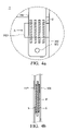
- FIG. 4 a is a perspective diagram of the second embodiment in accordance with the present invention.
- FIG. 4 b is a side view of the X direction corresponding to FIG. 3 a.
- the signal transmission device of the present invention comprises first, second and third flexible printed circuit boards 102 , 104 and 106 electrically connecting the touchscreen display module 10 and a system (not shown).
- the first flexible printed circuit board 102 communicates display panel signal between the touchscreen display module 10 and the system via the connector 1020 .
- the second and third flexible printed circuit boards 104 and 106 individually communicate a touch panel signal and a light source signal between the touchscreen display module 10 and the system through the first flexible printed circuit board 102 .
- the second and third flexible printed circuit boards 104 and 106 are joined to the first flexible printed circuit board 102 , thereby touch panel and light source signals from the touchscreen display module 10 can be collected in the first flexible printed circuit board 102 and communicated to the system via the connector 1020 . That is, the display panel, touch panel and light source signals are integrated in the first flexible printed circuit board 102 and communicated to the system through a single connector 1020 .
- the first and second flexible printed circuit boards 102 and 104 are joined by hot bar soldering via corresponding soldering pads S.
- the touch panel signal of the second flexible printed circuit board 104 is collected in the first flexible printed circuit board 102 .
- the second flexible printed circuit board 104 further comprises several longitudinal openings Hi adjacent to the soldering pads S preventing short circuits due to solder overflow.
- the opening H 1 can be also disposed in the first flexible printed circuit board 102 .
- the first flexible printed circuit board 102 defines a connection area 1021 with soldering pads S disposed thereon.
- several alignment marks M are correspondingly disposed around the periphery of the connection area 1021 and the second flexible printed circuit board 104 . Accurate positioning and connection is accomplished by aligning the alignment marks M on the first and second flexible printed circuit boards 102 and 104 during assembly.
- the alignment marks M can also be applied to the third flexible printed circuit board 106 for accurate connection of the first flexible printed circuit board 102 as shown by the area B in FIG. 2 .
- the first and second flexible printed circuit boards 102 and 104 are joined by anisotropic conductive film (ACF) bonding via corresponding soldering pads S.
- ACF anisotropic conductive film
- an anisotropic conductive film F is electrically bonded between the soldering pads S of the first and second flexible printed circuit boards 102 and 104 .
- the touch panel signal of the second flexible printed circuit board 104 can be collected in the first flexible printed circuit board 102 .
- the first and second flexible printed circuit boards 102 and 104 are aligned via alignment holes H 2 . Accurate positioning and connection is accomplished by aligning the alignment holes H 2 of the first and second flexible printed circuit board 102 and 104 . Similarly, the alignment hole H 2 can also be applied to the third flexible printed circuit board 106 for accurate connection of the first flexible printed circuit board 102 as shown by the area B in FIG. 2 .
- the present invention provides a signal transmission device capable of collecting touch panel and light source signals together in the first flexible printed circuit board 102 .
- touch panel, light source and display panel signals between the touchscreen display module 10 and the system can be communicated through a single connector 1020 of the flexible printed circuit board 102 .
- each flexible printed circuit board can be joined by hot bar soldering or anisotropic conductive film (ACF) bonding.
- ACF anisotropic conductive film
- the alignment marks M or openings H 2 can be applied to each flexible printed circuit board for accurate positioning and connection. As only a single connector is required to communicate the multiple signals between the touchscreen display module 10 and the system, fabrication cost and space required for assembly can be reduced.
Abstract
Description
Claims (23)
Applications Claiming Priority (2)
| Application Number | Priority Date | Filing Date | Title |
|---|---|---|---|
| TW93110823 | 2004-04-19 | ||
| TW093110823A TWI249717B (en) | 2004-04-19 | 2004-04-19 | Signal transmission device |
Publications (2)
| Publication Number | Publication Date |
|---|---|
| US20050233611A1 US20050233611A1 (en) | 2005-10-20 |
| US7090506B2 true US7090506B2 (en) | 2006-08-15 |
Family
ID=35096839
Family Applications (1)
| Application Number | Title | Priority Date | Filing Date |
|---|---|---|---|
| US10/921,462 Expired - Fee Related US7090506B2 (en) | 2004-04-19 | 2004-08-19 | Signal transmission device having flexible printed circuit boards |
Country Status (3)
| Country | Link |
|---|---|
| US (1) | US7090506B2 (en) |
| JP (1) | JP4574421B2 (en) |
| TW (1) | TWI249717B (en) |
Cited By (7)
| Publication number | Priority date | Publication date | Assignee | Title |
|---|---|---|---|---|
| US20060205245A1 (en) * | 2005-03-14 | 2006-09-14 | Au Optronics Corp. | Electronic device and flat panel display utilizing the same |
| US20090139750A1 (en) * | 2006-07-05 | 2009-06-04 | Fujitsu Limited | Printed wiring board and printed circuit board unit and electronic apparatus |
| US20110148777A1 (en) * | 2009-12-18 | 2011-06-23 | Innocom Technology (Shenzhen) Co., Ltd. | Method for bonding fpc onto baseboard, bonding assembly, and touch screen |
| US20120314113A1 (en) * | 2011-06-13 | 2012-12-13 | Samsung Electronics Co., Ltd. | Photographing apparatus and electronic device |
| US20190220122A1 (en) * | 2018-01-12 | 2019-07-18 | Samsung Display Co., Ltd. | Display device and flexible circuit board |
| US20220011617A1 (en) * | 2020-07-10 | 2022-01-13 | Samsung Display Co., Ltd. | Display device |
| US11670900B2 (en) | 2019-02-05 | 2023-06-06 | Emergency Technology, Inc. | Universal smart adaptor |
Families Citing this family (19)
| Publication number | Priority date | Publication date | Assignee | Title |
|---|---|---|---|---|
| KR20060085289A (en) * | 2005-01-21 | 2006-07-26 | 삼성전자주식회사 | Dual display device |
| KR101348247B1 (en) * | 2007-06-07 | 2014-01-09 | 삼성디스플레이 주식회사 | Liquid crystal display device |
| TWI365013B (en) | 2008-05-23 | 2012-05-21 | Au Optronics Corp | Flat panel display |
| TWI385618B (en) * | 2008-09-16 | 2013-02-11 | Novatek Microelectronics Corp | Transmission device with enhanced signals |
| KR20120019543A (en) * | 2010-08-26 | 2012-03-07 | 삼성전자주식회사 | On-cell tsp display device |
| KR101373047B1 (en) * | 2010-09-07 | 2014-03-11 | 삼성디스플레이 주식회사 | Flexible Printed Circuit Board and Touch Screen Panel Device Having the Same |
| CN102000933B (en) * | 2010-09-30 | 2013-09-18 | 无锡博一光电科技有限公司 | Liquid crystal display (LCD) welding fixture and welding method thereof |
| EP2638456B1 (en) * | 2010-11-11 | 2019-06-12 | TPK Touch Solutions (Xiamen) Inc. | Single-axis capacitive multi-touch panel, system and method |
| DE102010063387A1 (en) * | 2010-12-17 | 2012-06-21 | Semikron Elektronik Gmbh & Co. Kg | Circuit arrangement with at least two submodules |
| JP5740477B2 (en) | 2011-09-15 | 2015-06-24 | シャープ株式会社 | Display device |
| CN105138172B (en) * | 2011-11-27 | 2018-08-07 | 宸鸿科技(厦门)有限公司 | Touch sensing device and its manufacturing method |
| TWI513380B (en) | 2012-10-12 | 2015-12-11 | Au Optronics Corp | Electronic device |
| JP6143466B2 (en) * | 2013-01-10 | 2017-06-07 | 株式会社ジャパンディスプレイ | LCD with built-in touch panel |
| CN104360768B (en) * | 2014-11-10 | 2018-02-13 | 京东方科技集团股份有限公司 | Touch-control display module and electronical display product |
| KR102281849B1 (en) * | 2015-02-13 | 2021-07-26 | 삼성디스플레이 주식회사 | Touch screen panel |
| JP6771432B2 (en) * | 2017-06-27 | 2020-10-21 | 株式会社Joled | Flexible wiring board pair and display device |
| CN107817633A (en) * | 2017-10-26 | 2018-03-20 | 惠科股份有限公司 | Signal transmitting apparatus and display device |
| WO2019184361A1 (en) * | 2018-03-27 | 2019-10-03 | Guangdong Oppo Mobile Telecommunications Corp., Ltd. | Display screen assembly and electronic device |
| CN110839103A (en) * | 2018-08-17 | 2020-02-25 | 深圳富泰宏精密工业有限公司 | Electronic device and control method thereof |
Citations (5)
| Publication number | Priority date | Publication date | Assignee | Title |
|---|---|---|---|---|
| US5418691A (en) * | 1990-02-07 | 1995-05-23 | Canon Kabushiki Kaisha | Two printed circuit boards superiposed on one another both having position registry marks |
| US5592365A (en) * | 1993-12-21 | 1997-01-07 | Sharp Kabushiki Kaisha | Panel assembly structure and panel assembling method capable of achieving a highly reliable connection of electrode terminals even when the electrode terminals have a fine pitch |
| US5684550A (en) * | 1992-07-22 | 1997-11-04 | Hitachi, Ltd. | Liquid crystal display device having a diffuser integrally formed with a prism plate |
| US6045368A (en) * | 1998-06-01 | 2000-04-04 | Cadenhead; Jonathan | Means for accurately aligning and attaching an electrical part to a surface mount circuit |
| US20050185127A1 (en) * | 2004-02-25 | 2005-08-25 | Natsuko Fujiyama | Method of manufacturing liquid crystal display |
-
2004
- 2004-04-19 TW TW093110823A patent/TWI249717B/en active
- 2004-08-19 US US10/921,462 patent/US7090506B2/en not_active Expired - Fee Related
-
2005
- 2005-04-11 JP JP2005113112A patent/JP4574421B2/en active Active
Patent Citations (5)
| Publication number | Priority date | Publication date | Assignee | Title |
|---|---|---|---|---|
| US5418691A (en) * | 1990-02-07 | 1995-05-23 | Canon Kabushiki Kaisha | Two printed circuit boards superiposed on one another both having position registry marks |
| US5684550A (en) * | 1992-07-22 | 1997-11-04 | Hitachi, Ltd. | Liquid crystal display device having a diffuser integrally formed with a prism plate |
| US5592365A (en) * | 1993-12-21 | 1997-01-07 | Sharp Kabushiki Kaisha | Panel assembly structure and panel assembling method capable of achieving a highly reliable connection of electrode terminals even when the electrode terminals have a fine pitch |
| US6045368A (en) * | 1998-06-01 | 2000-04-04 | Cadenhead; Jonathan | Means for accurately aligning and attaching an electrical part to a surface mount circuit |
| US20050185127A1 (en) * | 2004-02-25 | 2005-08-25 | Natsuko Fujiyama | Method of manufacturing liquid crystal display |
Cited By (10)
| Publication number | Priority date | Publication date | Assignee | Title |
|---|---|---|---|---|
| US20060205245A1 (en) * | 2005-03-14 | 2006-09-14 | Au Optronics Corp. | Electronic device and flat panel display utilizing the same |
| US7204698B2 (en) * | 2005-03-14 | 2007-04-17 | Au Optronics Corp. | Circuit board solder connection with feature to prevent solder bridging |
| US20090139750A1 (en) * | 2006-07-05 | 2009-06-04 | Fujitsu Limited | Printed wiring board and printed circuit board unit and electronic apparatus |
| US20110148777A1 (en) * | 2009-12-18 | 2011-06-23 | Innocom Technology (Shenzhen) Co., Ltd. | Method for bonding fpc onto baseboard, bonding assembly, and touch screen |
| US20120314113A1 (en) * | 2011-06-13 | 2012-12-13 | Samsung Electronics Co., Ltd. | Photographing apparatus and electronic device |
| US20190220122A1 (en) * | 2018-01-12 | 2019-07-18 | Samsung Display Co., Ltd. | Display device and flexible circuit board |
| US10884532B2 (en) * | 2018-01-12 | 2021-01-05 | Samsung Display Co., Ltd. | Display device and flexible circuit board |
| US11670900B2 (en) | 2019-02-05 | 2023-06-06 | Emergency Technology, Inc. | Universal smart adaptor |
| US20220011617A1 (en) * | 2020-07-10 | 2022-01-13 | Samsung Display Co., Ltd. | Display device |
| US11703726B2 (en) * | 2020-07-10 | 2023-07-18 | Samsung Display Co., Ltd. | Display device |
Also Published As
| Publication number | Publication date |
|---|---|
| JP4574421B2 (en) | 2010-11-04 |
| TW200535761A (en) | 2005-11-01 |
| TWI249717B (en) | 2006-02-21 |
| US20050233611A1 (en) | 2005-10-20 |
| JP2005317957A (en) | 2005-11-10 |
Similar Documents
| Publication | Publication Date | Title |
|---|---|---|
| US7090506B2 (en) | Signal transmission device having flexible printed circuit boards | |
| US9864446B2 (en) | Touch screen-integrated display device | |
| KR100548683B1 (en) | Method for manufacturing circuit structure unit and liquid crystal device | |
| US7728945B2 (en) | Structure for circuit assembly | |
| US7070422B1 (en) | Flexible circuit board | |
| US10886643B2 (en) | Display device | |
| US6870590B2 (en) | Electrooptical unit with a flexible board and electronic apparatus | |
| WO2011045994A1 (en) | Flexible circuit board connection structure and display device | |
| US20060125995A1 (en) | Liquid crystal display with compact IC chip configuration | |
| CN102736316B (en) | Liquid crystal indicator | |
| JP2002314212A (en) | Connection structure between fiexible printed circuit and wiring board, its connection method, and liquid crystal display device and its manufacturing method | |
| WO2010013530A1 (en) | Display panel and display device provided with the same | |
| US20070126971A1 (en) | Dual-display device with rigid-flex printed board having bonded connection means | |
| US6628351B1 (en) | Liquid crystal display apparatus | |
| KR20060063176A (en) | Reel type tape carrier package and plasma display device adopting the same | |
| CN113301713A (en) | Printed circuit board, flexible circuit board, display panel and manufacturing method | |
| JP2008294114A (en) | Flexible printed circuit board and liquid crystal display device | |
| JPH10209202A (en) | Liquid crystal display | |
| CN102914890B (en) | Flexible PCB | |
| JP2008145753A (en) | Display device | |
| JP2008233358A (en) | Liquid crystal display device | |
| US7241148B2 (en) | Modules for fixing flexible printed circuit boards and flat display devices utilizing the same | |
| WO1998041067A1 (en) | Electronic parts module and electronic equipment | |
| KR100867502B1 (en) | Liquid crystal module | |
| KR100964557B1 (en) | Flexible-printed circuit board, method of fabricating the same and method for mounting of bare chip using the same |
Legal Events
| Date | Code | Title | Description |
|---|---|---|---|
| AS | Assignment |
Owner name: AU OPTRONICS CORP., TAIWAN Free format text: ASSIGNMENT OF ASSIGNORS INTEREST;ASSIGNORS:SUNG, KUANG-TAO;LAO, JUN-HSIAN;REEL/FRAME:015716/0471 Effective date: 20040504 |
|
| FPAY | Fee payment |
Year of fee payment: 4 |
|
| RR | Request for reexamination filed |
Effective date: 20091201 |
|
| RR | Request for reexamination filed |
Effective date: 20100624 |
|
| AS | Assignment |
Owner name: AU OPTRONICS CORP., TAIWAN Free format text: ASSIGNMENT OF ASSIGNORS INTEREST;ASSIGNOR:AU OPTRONICS CORP.;REEL/FRAME:025884/0016 Effective date: 20110302 Owner name: AU OPTRONICS CORPORATION AMERICA, TEXAS Free format text: ASSIGNMENT OF ASSIGNORS INTEREST;ASSIGNOR:AU OPTRONICS CORP.;REEL/FRAME:025884/0016 Effective date: 20110302 |
|
| RR | Request for reexamination filed |
Effective date: 20110131 |
|
| B1 | Reexamination certificate first reexamination |
Free format text: THE PATENTABILITY OF CLAIMS 1 AND 4 ARE CONFIRMED. CLAIMS 10 AND 12 ARE CANCELLED. CLAIMS 5, 9 AND 17 ARE DETERMINED TO BE PATENTABLE AS AMENDED. CLAIMS 11, 13-16 AND 18-23, DEPENDENT ON AN AMENDED CLAIM ARE, DETERMINED TO BE PATENTABLE. NEW CLAIM 24 IS ADDED AND DETERMINED TO BE PATENTABLE. CLAIMS 2, 3 AND 6-8 WERE NOT REEXAMINED. |
|
| RR | Request for reexamination filed |
Effective date: 20110610 |
|
| AS | Assignment |
Owner name: AU OPTRONICS CORP., TAIWAN Free format text: ASSIGNMENT OF ASSIGNORS INTEREST;ASSIGNORS:AU OPTRONICS CORPORATION AMERICA;AU OPTRONICS CORP.;SIGNING DATES FROM 20120828 TO 20120904;REEL/FRAME:028906/0370 |
|
| B2 | Reexamination certificate second reexamination |
Free format text: CLAIMS 10 AND 12 WERE PREVIOUSLY CANCELLED. CLAIMS 1-9, 11 AND 13-24 ARE CANCELLED. |
|
| FPAY | Fee payment |
Year of fee payment: 8 |
|
| REFU | Refund |
Free format text: REFUND - PAYMENT OF MAINTENANCE FEE, 8TH YEAR, LARGE ENTITY (ORIGINAL EVENT CODE: R1552); ENTITY STATUS OF PATENT OWNER: LARGE ENTITY |
|
| FEPP | Fee payment procedure |
Free format text: MAINTENANCE FEE REMINDER MAILED (ORIGINAL EVENT CODE: REM.) |
|
| LAPS | Lapse for failure to pay maintenance fees |
Free format text: PATENT EXPIRED FOR FAILURE TO PAY MAINTENANCE FEES (ORIGINAL EVENT CODE: EXP.); ENTITY STATUS OF PATENT OWNER: LARGE ENTITY |
|
| STCH | Information on status: patent discontinuation |
Free format text: PATENT EXPIRED DUE TO NONPAYMENT OF MAINTENANCE FEES UNDER 37 CFR 1.362 |
|
| FP | Lapsed due to failure to pay maintenance fee |
Effective date: 20180815 |