US9836312B2 - Storage control device, storage device, and storage control method thereof - Google Patents
Storage control device, storage device, and storage control method thereof Download PDFInfo
- Publication number
- US9836312B2 US9836312B2 US14/310,205 US201414310205A US9836312B2 US 9836312 B2 US9836312 B2 US 9836312B2 US 201414310205 A US201414310205 A US 201414310205A US 9836312 B2 US9836312 B2 US 9836312B2
- Authority
- US
- United States
- Prior art keywords
- memory
- area
- data
- saving
- preliminary
- Prior art date
- Legal status (The legal status is an assumption and is not a legal conclusion. Google has not performed a legal analysis and makes no representation as to the accuracy of the status listed.)
- Expired - Fee Related, expires
Links
Images


Classifications
-
- G—PHYSICS
- G06—COMPUTING; CALCULATING OR COUNTING
- G06F—ELECTRIC DIGITAL DATA PROCESSING
- G06F9/00—Arrangements for program control, e.g. control units
- G06F9/06—Arrangements for program control, e.g. control units using stored programs, i.e. using an internal store of processing equipment to receive or retain programs
- G06F9/44—Arrangements for executing specific programs
- G06F9/4401—Bootstrapping
- G06F9/4418—Suspend and resume; Hibernate and awake
-
- G—PHYSICS
- G06—COMPUTING; CALCULATING OR COUNTING
- G06F—ELECTRIC DIGITAL DATA PROCESSING
- G06F11/00—Error detection; Error correction; Monitoring
- G06F11/07—Responding to the occurrence of a fault, e.g. fault tolerance
- G06F11/14—Error detection or correction of the data by redundancy in operation
- G06F11/1402—Saving, restoring, recovering or retrying
- G06F11/1446—Point-in-time backing up or restoration of persistent data
-
- G—PHYSICS
- G06—COMPUTING; CALCULATING OR COUNTING
- G06F—ELECTRIC DIGITAL DATA PROCESSING
- G06F3/00—Input arrangements for transferring data to be processed into a form capable of being handled by the computer; Output arrangements for transferring data from processing unit to output unit, e.g. interface arrangements
- G06F3/06—Digital input from, or digital output to, record carriers, e.g. RAID, emulated record carriers or networked record carriers
- G06F3/0601—Interfaces specially adapted for storage systems
- G06F3/0668—Interfaces specially adapted for storage systems adopting a particular infrastructure
- G06F3/0671—In-line storage system
- G06F3/0683—Plurality of storage devices
- G06F3/0689—Disk arrays, e.g. RAID, JBOD
Definitions
- the present disclosure relates to a storage control device, and more particularly, to a storage control device that controls a saving process between memories, a storage device, a storage control method thereof, and a program that allows a computer to execute the method.
- the following suspension process and restoration process are used to cut off power of the information processing system while retaining data in operation. That is, as the suspension process, a host computer cuts off the power of the information processing system after saving all data in use on a main memory in an area that is secured in a storage memory. In addition, as the restoration process, the host computer restores the data that is saved in the storage memory to the main memory. In the related art, the data saving is carried out during shutdown.
- a device which includes flag data indicating whether or not data on a DRAM is synchronized with data on a flash memory, and which only transmits data necessary for synchronization to a flash memory on the basis of flag data during shutdown, is suggested (for example, refer to Japanese Unexamined Patent Application Publication No. 2011-186558).
- a storage control device and a storage control method thereof.
- the storage control device comprises: a detection unit configured to determine whether a preliminary process of saving data from a first memory to a second memory is necessary, wherein the second memory includes a suspend area and a typical area; a preliminary processing unit configured to write a first value to the suspend area when the detection unit has determined that the preliminary process is necessary; and a saving processing unit configured to write a second value corresponding to the data, wherein the first value is different from the second value when the detection unit has determined that the preliminary process is necessary.
- the preliminary process is carried out with respect to the data for which the necessity for saving is detected, and thus processes during the saving can be reduced.
- a storage device including: a first memory configured to store data; a second memory configured to save the data stored in the first memory and including a suspend area and a typical area; a detection unit configured to determine whether a preliminary process of saving data from the first memory to the second memory is necessary; a preliminary processing unit configured to write a first value to the suspend area when the detection unit has determined that the preliminary process is necessary; and a saving processing unit configured to write a second value corresponding to the data, wherein the first value is different from the second value when the detection unit has determined that the preliminary process is necessary.
- a storage control method comprising: determining, by a detection unit, whether a preliminary process of saving data from a first memory to a second memory is necessary, wherein the second memory includes a suspend area and a typical area; writing, by a preliminary processing unit, a first value to the suspend area for data for which the detection unit has determined that the preliminary process is necessary; and writing, by a saving processing unit, a second value corresponding to the data, wherein the first value is different from the second value when the detection unit has determined that the preliminary process is necessary.
- FIG. 1 is a diagram illustrating a configuration example of an information processing system according to a first embodiment of the present disclosure
- FIG. 2 is a diagram illustrating a functional configuration example of the information processing system according to the embodiment of the present disclosure
- FIG. 3 is a diagram illustrating a resistance state of a resistance-variable memory
- FIGS. 4A to 4C are diagrams illustrating an example of a voltage pulse that is applied to a memory cell of a storage memory according to the embodiment of the present disclosure
- FIG. 5 is a diagram illustrating an example of a dirty flag according to the embodiment of the present disclosure.
- FIG. 6 is a diagram illustrating an example of a preliminary process flag according to the embodiment of the present disclosure.
- FIG. 7 is a flowchart illustrating a procedure example of a restoration process according to the first embodiment of the present disclosure
- FIG. 8 is a flowchart illustrating a procedure example of a writing process in a main memory according to the first embodiment of the present disclosure
- FIG. 9 is a flowchart illustrating a procedure example of a writing process in a storage memory according to the first embodiment of the present disclosure.
- FIG. 10 is a flowchart illustrating a procedure example of a preliminary process on the storage memory according to the first embodiment of the present disclosure
- FIG. 11 is a flowchart illustrating a procedure example of a saving process in the storage memory according to the first embodiment of the present disclosure
- FIG. 12 is a diagram illustrating a configuration example of an information processing system according to a second embodiment of the present disclosure.
- FIG. 13 is a flowchart illustrating a procedure example of a writing process in a main memory according to the second embodiment of the present disclosure
- FIG. 14 is a flowchart illustrating a procedure example of a saving process in a storage memory according to the second embodiment of the present disclosure
- FIG. 15 is a diagram illustrating a configuration example of an information processing system according to a first modification example of the present disclosure
- FIG. 16 is a diagram illustrating a configuration example of an information processing system according to a second modification example of the present disclosure
- FIG. 17 is a diagram illustrating a configuration example of an information processing system according to a third modification example of the present disclosure.
- FIG. 18 is a diagram illustrating an example of a dirty flag and a preliminary process flag according to a fourth modification example of the present disclosure
- FIG. 19 is a diagram illustrating a relational example between a dirty flag and a saving area according to a fifth modification example of the present disclosure.
- FIGS. 20A to 20C are diagrams illustrating an example of a voltage pulse that is applied to a memory cell of a storage memory according to a sixth modification example of the present disclosure
- FIGS. 21A to 21C are diagrams illustrating an example of a voltage pulse that is applied to a memory cell of a storage memory according to an eleventh modification example of the present disclosure
- FIGS. 22A to 22C are diagrams illustrating an example of a voltage pulse that is applied to a memory cell of a saving area of a storage memory according to a twelfth modification example of the present disclosure
- FIG. 23 is a flowchart illustrating a procedure example of a writing process in a storage memory according to the twelfth modification example of the present disclosure
- FIG. 24 is a flowchart illustrating a procedure example of a saving process in the storage memory according to the twelfth modification example of the present disclosure
- FIGS. 25A to 25C are diagrams illustrating an example of a voltage pulse that is applied to a memory cell of a saving area of a storage memory according to a thirteenth modification example of the present disclosure
- FIG. 26 is a diagram illustrating a configuration example of an information processing system according to a fifteenth modification example of the present disclosure.
- FIG. 27 is a diagram illustrating a configuration example of a main memory management table according to the fifteenth modification example of the present disclosure.
- FIG. 28 is a diagram illustrating a configuration example of an application state flag according to the fifteenth modification example of the present disclosure.
- FIG. 29 is a flowchart illustrating a procedure example of a writing process in a main memory according to the fifteenth modification example of the present disclosure
- FIG. 30 is a flowchart illustrating a procedure example of an allocation changing process in the main memory according to the fifteenth modification example of the present disclosure
- FIG. 31 is a flowchart illustrating a procedure example of a monitoring process of the application state flag according to the fifteenth modification example of the present disclosure
- FIG. 32 is a flowchart illustrating a procedure example of a restoration process according to a sixteenth modification example of the present disclosure
- FIG. 33 is a flowchart illustrating a procedure example of a saving process in a storage memory according to the sixteenth modification example of the present disclosure.
- FIG. 34 is a diagram illustrating a resistance state of a resistance-variable memory according to the sixteenth modification example of the present disclosure.
- FIG. 1 shows a diagram illustrating a configuration example of an information processing system according to a first embodiment of the present disclosure.
- the information processing system includes a host computer 100 , a main memory 200 , and a storage module 300 .
- a process of saving data, which is stored in the main memory 200 , in the storage module 300 is referred to as a “saving process.”
- a process of restoring data, which is saved in the storage module 300 , to the main memory 200 is referred to as a “restoration process.”
- the main memory 200 and the storage module 300 constitute a memory system.
- the host computer 100 instructs or carries out each process in the information processing system.
- the host computer 100 includes a main memory interface 120 for connection with the main memory 200 and a storage interface 130 for connection with the storage module 300 .
- the main memory 200 is a memory that is used by the host computer 100 to carry out each process.
- the main memory 200 is constituted by a volatile memory such as a DRAM.
- the main memory 200 is connected to the host computer 100 through a signal line 209 .
- the main memory 200 is an example of a first memory described in claims.
- the storage module 300 is a storage module that is used by the host computer 100 as an auxiliary storage.
- the storage module 300 is connected to the host computer 100 through a signal line 309 .
- the storage module 300 includes a storage memory 320 that stores data, and a storage controller 310 that controls the storage memory 320 .
- the storage memory 320 is constituted by a nonvolatile memory such as a resistance-variable memory (ReRAM).
- the storage memory 320 is divided into a saving area (suspend area) 321 where data of the main memory 200 is stored during system pause, and a typical area for typical data storage.
- the storage memory 320 is an example of a second memory described in claims.
- the storage controller 310 includes an error check and correction (ECC) processing unit 311 that corrects an error of the storage memory 320 .
- ECC error check and correction
- the ECC processing unit 311 is provided to the storage controller 310 , but may be provided to the host computer 100 or the storage memory 320 .
- the main memory 200 includes a dirty flag 211 and a preliminary process flag 212 for each predetermined area.
- the dirty flag 211 is a flag that retains whether or not writing of data with respect to an area after being subjected to an immediately previous restoration process has been carried out.
- the preliminary process flag 212 is a flag that retains whether or not a necessary preliminary process has been carried out with respect to the area. A specific example of the dirty flag 211 and the preliminary process flag 212 will be described later.
- FIG. 2 shows a diagram illustrating a functional configuration example of the information processing system according to this embodiment of the present disclosure.
- a main memory 20 corresponds to the above-described main memory 200 .
- the storage memory 30 corresponds to the above-described storage memory 320 .
- Each cell of the main memory 20 and the storage memory 30 stores any one value of binary values “0” and “1” as bit data.
- the restoration processing unit 11 carries out a restoration process of restoring data, which is saved in a saving area of the storage memory 30 , to the main memory 20 .
- the detection unit 14 detects necessity for a preliminary process during saving of data, which is stored in the main memory 20 , in a corresponding saving area of the storage memory 30 .
- the detection unit 14 detects the necessity for the preliminary process on the basis of the preliminary process flag 212 .
- the preliminary processing unit 12 carries out a preliminary process in which one value of the binary values is written with respect to a saving area of data, for which necessity for the preliminary process is detected by the detection unit 14 , in the storage memory 30 .
- the preliminary process is carried out before the saving process to speed up the saving process.
- the saving processing unit 13 writes a value corresponding to data to be saved with respect to a saving area in the storage memory 30 in which one of the binary values is written. With respect to a saving area for which a preliminary process is carried out, the other value of the binary values is written according to data to be saved. On the other hand, with respect to a saving area for which a preliminary process is not carried out, either one value or the other value of the binary values is written according to data to be saved.
- FIG. 3 shows a diagram illustrating a resistance state of a resistance-variable memory.
- a memory cell of the resistance-variable memory transitions to a low resistance state (LRS) by a set operation, and transitions to a high resistance state (HRS) by a reset operation.
- LRS low resistance state
- HRS high resistance state
- a resistance state is determined on the basis of a reference resistance value that is shown as a read threshold value.
- a reference resistance value that is shown as a read threshold value.
- FIGS. 4A to 4C show diagrams illustrating an example of a voltage pulse that is applied to a memory cell of the storage memory 30 according to the embodiment of the present disclosure.
- FIG. 4A illustrates a type of voltage pulse in a case of typical writing.
- a typical writing operation is classified into three processes of a pre-read process, a reset process, and a set process.
- description will be made here with respect to an example in which the reset process is carried out first and then the set process is carried out.
- the set process may be carried out first and then the reset process may be carried out.
- the pre-read process is a process of reading out a current value of a writing destination address, and comparing the value and data to be written from this with each other.
- the reset process is a process of selecting a bit cell to be inverted from “1” to “0” among respective bit cells of the address on the basis of the comparison result obtained in the pre-read process, and writing “0”.
- the set process is a process of selecting a bit cell to be inverted from “0” to “1” among the respective bit cells of the address on the basis of a comparison result obtained in the pre-read process, and writing “1”.
- the reset process is carried out by selecting only the lowermost bit, and then the set process is carried out by selecting only the uppermost bit.
- the second bit and the third bit existing values are retained without carrying out any process.
- an access unit to the storage memory 30 is set as 2 KB, and total time necessary for the pre-read process, the reset process, and the set process is set as 2 ⁇ s (microsecond), a transmission rate becomes 1 GB/second.
- a method in which operations other than the set process in the typical writing are carried out in advance is carried out to speed up the saving process. That is, as shown in FIG. 4B , when writing in the main memory 20 occurs, as a preliminary process, the pre-read process and the reset process are carried out in advance with respect to the saving area of the storage memory 30 . According to this, when carrying out the saving process, as shown in FIG. 4C , only the set process may be carried out and thus the high speed of the saving process may be realized. The writing according to only the set process is referred to as high-speed writing.
- the transmission rate during the high-speed writing according to this embodiment of the present disclosure becomes 2 GB/second.
- the saving process may be carried out in a state in which the preliminary process is not carried out in time due to an arbitrary reason. In this case, it is necessary to carry out the pre-read process, the reset process, and the set process according to the typical writing.
- FIG. 5 shows a diagram illustrating an example of the dirty flag 211 according to the embodiment of the present disclosure.
- the dirty flag 211 is a flag that retains whether or not writing of data with respect to an area after being subjected to an immediately previous restoration process has been carried out.
- the dirty flag 211 is stored on the main memory 200 , and the host computer 100 updates the dirty flag 211 by using the main memory interface 120 with reference to the same.
- the dirty flag 211 is provided for each word of the main memory 200 in a corresponding manner, and retains a flag of one bit.
- the dirty flag 211 is set to “1”, and when the saving process is carried out, the dirty flag 211 is set to “0”.
- FIG. 6 shows a diagram illustrating an example of the preliminary process flag 212 according to the embodiment of the present disclosure.
- the preliminary process flag 212 is a flag that retains whether or not a necessary preliminary process has been carried out with respect to the area.
- the preliminary process flag 212 is stored on the main memory 200 , and the host computer 100 updates the preliminary process flag 212 using the main memory interface 120 with reference to the same.
- the preliminary process flag 212 is provided for each word of the main memory 200 in a corresponding manner, and retains a flag of one bit.
- the preliminary process flag 212 is set to “1”, and when the preliminary process is completed, the preliminary process flag 212 is set to “0”.
- this case means that a preliminary process to be carried out with respect to the word is present. That is, in a case where the dirty flag 211 shows “1” and the preliminary process flag 212 shows “1”, this case means that a necessary preliminary process is not carried out. In a case where the dirty flag 211 shows “1” and the preliminary process flag 212 shows “0”, this case means that a necessary preliminary process is carried out.
- the preliminary process flag 212 also becomes “0”. This case means that a preliminary process to be carried out with respect to the word is not present.
- FIG. 7 shows a flowchart illustrating a procedure example of the restoration process according to the first embodiment of the present disclosure.
- FIG. 8 shows a flowchart illustrating a procedure example of a writing process in the main memory 200 according to the first embodiment of the present disclosure.
- the host computer 100 writes data in the main memory 200 during a course of carrying out various processes (step S 921 ).
- an address at which data is written is set as an address P.
- the host computer 100 sets the dirty flag 211 and the preliminary process flag 212 , which correspond to the address P, to “1” (step S 922 ).
- FIG. 9 shows a flowchart illustrating a procedure example of a writing process in a storage memory 320 according to the first embodiment of the present disclosure.
- the host computer 100 may write data in the storage memory 320 during the course of carrying out various processes (step S 931 ).
- a typical area for typical writing is present in the storage memory 320 .
- typical writing is used instead of high-speed writing.
- FIG. 10 shows a flowchart illustrating a procedure example of a preliminary process on the storage memory 320 according to the first embodiment of the present disclosure.
- the host computer 100 checks necessity for the preliminary process for regular constant time intervals with respect to each address of the main memory 200 .
- an address that is an object of the preliminary process is set as an address R.
- As an initial value, “0” is set in R (step S 941 ).
- the host computer 100 refers to the preliminary process flag 212 that corresponds to the address R (step S 942 ).
- the host computer 100 carries out the pre-read process and the reset process with respect to the saving area of the storage memory 320 which corresponds to the address R (step S 944 ).
- “0” is written in all bits of the saving area that correspond to the address R of the storage memory 320 .
- the preliminary process flag 212 is set to “0” (step S 945 ).
- these processes are not carried out.
- step S 946 The above-described processes are repeated until they reach an end address (step S 946 ) while adding a value of R one by one (step S 947 ).
- the host computer 100 may sequentially transmit a command for carrying out the pre-read process, data in which all bits are set to “0”, and a command for carrying out the reset process with respect to the storage module 300 .
- a dedicated command for carrying out a preliminary process may be prepared, and only the command may be transmitted without transmitting data “0”.
- FIG. 11 shows a flowchart illustrating a procedure example of a saving process in the storage memory 320 according to the first embodiment of the present disclosure.
- the host computer 100 refers to the dirty flag 211 that corresponds to the address Q (step S 952 ).
- the dirty flag 211 shows “1” (Yes in step S 953 )
- the following processes up to step S 961 relating to the address Q are carried out.
- the processes relating to the address Q are not carried out.
- the host computer 100 refers to the preliminary process flag 212 that corresponds to the address Q (step S 954 ).
- the preliminary process flag 212 shows “0” (Yes in step S 955 )
- data is read out from the address Q of the main memory 200 (step S 956 ), and high-speed writing is carried out in the saving area 321 of the address Q (step S 957 ). That is, in this case, writing according to only the set process is carried out with respect to the storage memory 320 .
- step S 955 data is read out from the address Q of the main memory 200 (step S 958 ), and the typical writing is carried out in the saving area 321 of the address Q (step S 959 ). That is, in this case, writing according to the pre-read process, the reset process, and the set process are carried out with respect to the storage memory 320 .
- step S 957 or step S 959 the dirty flag 211 that corresponds to the address Q is cleared to “0” (step S 961 ).
- step S 962 The above-described processes are repeated until they reach an end address (step S 962 ) while adding a value of Q one by one (step S 963 ).
- necessity for saving is detected using the preliminary process flag 212 , and the preliminary process is carried out on the basis of a detection result, and thus high-speed saving process can be realized.
- FIG. 12 shows a diagram illustrating a configuration example of an information processing system according to a second embodiment of the present disclosure.
- the information processing system according to the second embodiment is the same as the case of the first embodiment, and thus description thereof will not be repeated here.
- the second embodiment is different from the first embodiment in that the preliminary process flag 212 is not provided.
- the host computer 100 quickly carries out the preliminary process whenever writing in the main memory 200 is carried out. That is, in the second embodiment, the detection unit 14 detects necessity for the saving according to writing in the main memory 200 . According to this, the preliminary process may be completed before the saving process is carried out without using the preliminary process flag 212 .
- FIG. 13 shows a flowchart illustrating a procedure example of a writing process in the main memory 200 according to the second embodiment of the present disclosure.
- the host computer 100 writes data in the main memory 200 during the course of carrying out various processes (step S 921 ).
- an address at which data is written is set as an address P.
- the host computer 100 sets the dirty flag 211 , which corresponds to the address P, to “1” (step S 923 ).
- the pre-read process and the reset process are carried out with respect to a saving area of the storage memory 320 which corresponds to the address P (step S 924 ).
- FIG. 14 shows a flowchart illustrating a procedure example of the saving process in the storage memory 320 according to the second embodiment of the present disclosure.
- the host computer 100 refers to the dirty flag 211 that corresponds to the address Q (step S 952 ).
- the dirty flag 211 shows “1” (Yes in step S 953 )
- the following processes up to step S 961 regarding the address Q are carried out.
- the process regarding the address Q is not carried out.
- the host computer 100 reads out data from the address Q of the main memory 200 (step S 956 ), and high-speed writing in the saving area 321 of the address Q is carried out (step S 957 ). That is, writing is carried out only in the set process with respect to the storage memory 320 .
- a preliminary process is carried out during the writing in the main memory 200 , and thus the saving process according to the typical writing is not carried out.
- step S 957 the dirty flag 211 that corresponds to the address Q is cleared to “0” (step S 961 ).
- step S 962 The above-described processes are repeated until they reach an end address (step S 962 ) while adding a value of Q one by one (step S 963 ). After the processes are carried out until they reach the end address (Yes in step S 962 ), the host computer 100 is notified of an instruction indicating that data saving is completed (step S 964 ).
- the necessity for saving is detected according to the writing in the main memory 200 , and the preliminary process is carried out on the basis of the detection result, and thus high-speed saving process can be realized.
- FIG. 15 shows a diagram illustrating a configuration example of an information processing system according to a first modification example of the present disclosure.
- data transmission between the main memory 200 and the storage module 300 is carried out according to an instruction from the host computer 100 , but in the first modification example, the data transmission is carried out without mediation of the host computer 100 .
- the main memory 200 and the storage module 300 are connected through a signal line 208 , and a mechanism that directly carries out data transmission through the signal line 208 is provided.
- the host computer 100 only transmits a saving command to the storage controller 310 by using the mechanism without reading out data from the main memory 200 .
- the storage controller 310 that receives the saving command autonomously carries out the saving process shown in FIG. 11 . That is, the storage controller 310 refers to the dirty flag 211 and the preliminary process flag 212 on the main memory 200 , and carries out data saving from the main memory 200 to the storage memory 320 in response to the reference value.
- “saving completion” is notified from the storage controller 310 to the host computer 100 .
- the saving process is carried out during system suspension, after the host computer 100 issues the saving command, writing is not carried out with respect to an area of the main memory 200 in which data is saved before receiving “saving completion”.
- a user may carry out a keyboard operation and the like, and thus it may be necessary for the writing in the area of the main memory 200 , in which data is saved, to be carried out.
- the host computer 100 continues writing in the main memory 200 after transmitting a command indicating “saving stoppage” to the storage controller 310 .
- the storage controller 310 sets the dirty flag 211 of an address during the saving process to “1”, and completes the saving process. In this case, the completion notification from the storage controller 310 to the host computer 100 is not carried out.
- the storage controller 310 autonomously carries out the restoration process shown in FIG. 7 , and then notifies the host computer 100 of “restoration completion”. After issuing the restoration command, the host computer 100 does not carry out an access to the main memory 200 of an area to be restored before receiving “restoration completion”.
- the storage controller 310 autonomously carries out the preliminary process shown in FIG. 10 without an instruction from the host computer 100 .
- the preliminary process may be carried out by the host computer 100 .
- FIG. 16 shows a diagram illustrating a configuration example of an information processing system according to a second modification example of the present disclosure.
- the host computer 100 individually gives an instruction to the main memory 200 and the storage memory 320 .
- the main memory 200 and the storage memory 320 are handled in a unified manner. That is, the main memory 200 and the storage memory 320 are unified in a unified memory module 400 and are controlled by a unified memory controller 410 of the unified memory module 400 .
- the host computer 100 includes a memory interface 140 for connection to the unified memory module 400 .
- the unified memory controller 410 is connected to the memory interface 140 through a signal line 409 .
- the unified memory controller 410 includes an ECC processing unit 411 that corrects an error of the storage memory 320 .
- the ECC processing unit 411 is provided to the unified memory controller 410 , but may be provided to the host computer 100 or the storage memory 320 .
- the host computer 100 in the saving process or the restoration process, the host computer 100 only transmits a command of initiation of saving or initiation of restoration to the unified memory controller 410 , and the saving process or the restoration process is carried out by the unified memory controller 410 . Similar to this, the preliminary process is also autonomously carried out by the unified memory controller 410 . Further, in the second modification example, when writing in the main memory 200 from the host computer 100 is carried out, an operation of setting the dirty flag 211 and the preliminary process flag 212 of a corresponding address to “1” is also carried out by the unified memory controller 410 .
- data transmission control between the main memory 200 and the storage memory 320 can be independently carried out by the unified memory module 400 without mediation of the host computer 100 .
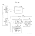
- FIG. 17 shows a diagram illustrating a configuration example of an information processing system according to a third modification example of the present disclosure.
- the dirty flag 211 and the preliminary process flag 212 are retained by the main memory 200 .
- a dedicated flag memory 330 is provided to the storage module 300 .
- the flag memory 330 retains the flag as the dirty flag 331 and the preliminary process flag 332 .
- the host computer 100 carries out updating with reference to the dirty flag 331 and the preliminary process flag 332 by using the storage interface 130 .
- a partial region of the main memory 200 is used for writing of a flag, but in the third modification example, the main memory 200 is not used.
- access to the flag is carried out for reading-out and writing in a bit unit, and thus when a dedicated memory in which an access unit is smaller than that of the main memory 200 is provided, access delay or power consumption can be reduced.
- FIG. 18 shows a diagram illustrating an example of a dirty flag 211 and a preliminary process flag 212 according to a fourth modification example of the present disclosure.
- the main memory 200 includes the dirty flag 211 of one bit and the preliminary process flag 212 of one bit.
- the host computer 100 sets a corresponding dirty flag 211 to “1”.
- the dirty flag 211 and the preliminary process flag 212 are provided for each specific address range, and thus a storage area necessary for both of the flags can be reduced.
- FIG. 19 shows a diagram illustrating a relational example between the dirty flag 211 and the saving area according to a fifth modification example of the present disclosure.
- An address space of the main memory 200 is divided into plural parts (for example, spaces 221 and 222 ) having an arbitrary size, and dirty flags 231 and 232 are provided with the respective spaces set as virtual address spaces.
- a saving area that corresponds to each dirty flag is prepared in one or more number of saving areas with respect to one dirty flag.
- saving areas 322 and 323 are prepared for the dirty flag 231
- saving areas 324 and 325 are prepared for the dirty flag 232 .
- a pointer that indicates a position of the saving area is provided for each dirty flag so as to discriminate to which saving area the dirty flag corresponds.
- the pointer means a leading address of the saving area that corresponds to the dirty flag in a total address space of the storage memory 320 .
- power saving of a system may be realized by carrying out the data saving with respect to only an arbitrary memory chip, and by shutting off or limiting power supply to the memory chip.
- a dirty flag of a memory space that is allocated for the application may be created.
- a part of the main memory may be opened or power thereof may be shut off.
- FIGS. 20A to 20C show diagrams illustrating a voltage pulse that is applied to a memory cell of a storage memory according to the sixth modification example of the present disclosure.
- the reset process and the set process regardless whether a current state of a bit cell before writing is “1” or “0”, when the bit of data that is written is “1”, a set pulse is applied to total bits, and when the bit is “0”, a reset pulse is applied to the total bits. Accordingly, the reset process is carried out without carrying out the pre-read process in the preliminary process according to writing data, and the set process is carried out in the high-speed writing according to writing data.
- the sixth modification example it is possible to save a time necessary for the pre-read process in comparison to the first embodiment, and thus a total writing time becomes fast.
- the pre-read process is not carried out, there is a possibility that the same value may be successively written in a bit cell, and thus consumption of a rewriting lifespan of the cell may speed up. Accordingly, it is necessary to select the content of the writing operation according to characteristics of the storage memory 320 .
- the set process is carried out after carrying out the reset process.
- the reset process may be carried out after carrying out the set process. That is, when referring to the preliminary process flag of the address R, in a case where the value thereof is “1”, “1” is written to all bits of the address in the pre-read process and the set process.
- the set process when referring to the preliminary process flag of the address Q, in a case where the value thereof is “0”, the set process is carried out in advance, and thus data of the main memory 200 in the address Q can be written in the saving area according to only the reset process.
- the host computer 100 when writing in the main memory 200 occurs, the host computer 100 updates the dirty flag 211 and the preliminary process flag 212 , but the operation may be carried out by a component other than the host computer 100 .
- the host computer 100 transmits a write destination address of the main memory 200 to the storage controller 310 .
- the storage controller 310 can update the dirty flag 211 and the preliminary process flag 212 .
- the unified memory controller 410 typically receives a writing address in the main memory 200 from the host computer 100 . Accordingly, instead of the host computer 100 , the unified memory controller 410 can update the dirty flag 211 and the preliminary process flag 212 .
- the host computer 100 carries out the preliminary process with reference to the preliminary process flag 212 for regular constant time intervals, but the operation may be carried out by a component other than the host computer 100 .
- storage controller 310 can access to the dirty flag 211 or the preliminary process flag 212 without mediation of the host computer 100 .
- the unified memory controller 410 of the second modification example can access to the dirty flag 211 or the preliminary process flag 212 without mediation of the host computer 100 .
- the preliminary process can be carried out for regular constant time intervals without an instruction from the host computer 100 .
- the host computer 100 carries out the saving process and the restoration process, but these processes may be carried out by a component other than the host computer 100 .
- the storage controller 310 may carry out the saving process or the restoration process after receiving an initiation instruction from the host computer 100 .
- the unified memory controller 410 of the second modification example may carry out the saving process or the restoration process after receiving an initiation instruction from the host computer 100 .
- a command that indicates “initiation of saving” or “initiation of restoration” may be transmitted to the storage controller 310 or the unified memory controller 410 from the host computer 100 .
- Reference of the dirty flag 211 or the preliminary process flag 212 , and data transmission between the main memory 200 and the storage memory 320 are carried out by the storage controller 310 or the unified memory controller 410 .
- the storage controller 310 or the unified memory controller 410 notifies the host computer 100 of completion of saving or restoration.
- the host computer 100 turns off power of the main memory 200 , the storage memory 320 , the storage controller 310 or the unified memory controller 410 , and the like. In this case, the entirety of a system may be allowed to transition to a power saving state without turning off the power.
- the pulse application for each of the reset process and the set process is carried out once.
- the pulse application may be appropriately carried out in plural times during each of the reset process and the set process. For example, since a variation is present in writing characteristics of cells, with regard to the majority of cells, normal writing is possible with two times of pulse. On the other hand, four times of pulse may be necessary for normal writing in a minute number of remaining cells.
- FIGS. 21A to 21C show diagrams illustrating an example of a voltage pulse that is applied to a memory cell of the storage memory 30 according to the eleventh modification example of the present disclosure.
- the reset process is carried out by one or more times of reset pulse and 0 or more times of verification read.
- a voltage for writing of “0” in a bit cell is applied by the reset pulse for a constant time, and then a bit cell state is read out by the verification read. Then, it is examined whether or not “0” is correctly written.
- the reset pulse is applied again with respect to a bit cell for which correct writing is not carried out with the pulse of the first time, and then the verification read is carried out. These are repeated N times, and then the reset process is completed.
- a voltage for writing of “1” in a bit cell is applied by a set pulse for a constant time, and then a process of verification read is repeated M times.
- the pre-read process and the reset process are carried out during the preliminary process, and the set process is carried out during the subsequent saving process.
- the pre-read process and the set process may be carried out during the preliminary process, and the reset process may be carried out during the subsequent saving process.
- the pre-read process may be omitted depending on characteristics of the storage memory 320 .
- N times of reset pulse application and M times of set pulse application are applied, but the number of pulse applications may be reduced with respect to the saving process.
- the number of pulse applications in the typical writing is set in such a manner that even when a power shut-off state is maintained for a long period of time (for example, 10 years), sufficient reliability can be maintained. According to this, when reducing the number of pulse applications, occurrence of errors increases in comparison to a case of the typical writing. However, retention of data can be guaranteed for a short period of time (for example, one week) on the assumption of use of the ECC.
- FIGS. 22A to 22C show diagrams illustrating an example of a voltage pulse that is applied to a memory cell of the saving area of the storage memory 30 according to the twelfth modification example of the present disclosure.
- the number of pulse applications in the reset process and the set process is reduced by half in comparison to the writing in the typical area. That is, in the reset process, N/2 times of reset pulse application and N/2 times of verification are carried out, and in the set process, N/2 times of set pulse application and N/2 times of verification are carried out.
- the pre-read process and the reset process are carried out during the preliminary process, and the set process is carried out during the subsequent saving process.
- the pre-read process and the set process may be carried out during the preliminary process, and the reset process may be carried out during the subsequent saving process.
- the pre-read process may be omitted depending on characteristics of the storage memory 320 .
- FIG. 23 shows a flowchart illustrating a procedure example of the writing process in the storage memory 320 according to the twelfth modification example of the present disclosure.
- the number of pulse applications is reduced by half.
- writing with a typical number of pulse applications, which is not reduced by half is carried out (step S 932 ).
- FIG. 24 shows a flowchart illustrating a procedure example of the saving process in the storage memory 320 according to the twelfth modification example of the present disclosure.
- the procedure example in the twelfth modification example is basically the same as the saving process in the first embodiment shown in FIG. 11 .
- the procedure example of the twelfth modification example is different from that of the first embodiment in that the number of pulse application is reduced by half when carrying out writing in the saving area (step S 967 ).
- the number of pulse applications when carrying out writing in the saving area is reduced in comparison to a case of the typical area, and thus high-speed saving process can be realized.
- FIGS. 25A to 25C show diagrams illustrating an example of a voltage pulse that is applied to a memory cell of the saving area of the storage memory 30 according to a thirteenth modification example of the present disclosure.
- a pulse width during the reset process and the set process is reduced by half in comparison to the writing in the typical area.
- a pulse width when carrying out the writing in the saving area is made narrower in comparison to a case of the typical area, and thus high-speed saving process can be realized.
- the pulse width of the writing pulse is made narrow, but a voltage or a current may be made weak with respect to the writing pulse. That is, in the writing with respect to the saving area, a pulse application voltage during the reset process and the set process may be made lower in comparison to the writing with respect to the typical area.
- a current of a pulse during the reset process and the set process may be made smaller in comparison to the writing with respect to the typical area.
- the host computer 100 may carry out reading-out and rewriting of data with respect to the entirety of the saving area for every constant period (for example, for every week).
- the host computer 100 may transmit a refresh command to the storage controller 310 for every constant period, and the storage controller 310 may carry out the reading-out and rewriting of data with respect to the entirety of the saving area in response to the refresh command.
- the dirty flag 211 is set to “1” whenever the writing in the main memory 200 is carried out from the host computer 100 (step S 922 ), but the setting to “1” may be carried out at a different timing.
- an address at which writing is to be carried out in the future is predicted, and then the dirty flag 211 that corresponds to the address is set to “1”. That is, a virtual address that can be allocated for each application is managed, and then when a change occurs at the allocation, the dirty flag 211 and the preliminary process flag 212 , which correspond to the address, is set to “1”.
- FIG. 26 shows a diagram illustrating a configuration example of an information processing system according to the fifteenth modification example of the present disclosure.
- the fifteenth modification example is different from the first embodiment in that a main memory management table 213 and an application state flag 214 are provided in the main memory 200 , but the other configurations are the same as the first embodiment.
- the main memory management table 213 is a table indicating in which manner a virtual address recognized by each of the applications corresponds to each physical address of the main memory.
- the application state flag 214 is a flag indicating a list of applications during operation, and whether or not data updating has been carried out after an immediately previous restoration process with respect to each of the applications. For example, in a case where the flag is “0”, this case indicates that updating has not been carried out after the immediately previous restoration process, and in a case where the flag is “1”, this case indicates that updating has been carried out after the immediately previous restoration process.
- FIG. 27 shows a diagram illustrating a configuration example of the main memory management table 213 according to the fifteenth modification example of the present disclosure.
- the main memory management table 213 manages an application of an allocation destination and a virtual address thereof in correspondence with each address of the main memory 200 . With respect to an address that is not allocated to any application, indication of “empty” is shown.
- the host computer 100 allocates an empty area of the main memory 200 with the number necessary for the application. At this time, a pair of new allocation destination (application) and virtual address is written in a corresponding address item of the main memory management table 213 . In addition, when the application is completed, or when a part of the memory area occupied by the application during activation is opened, a corresponding address item of the main memory management table 213 is rewritten to “empty”.
- FIG. 28 shows a diagram illustrating a configuration example of an application state flag 214 according to the fifteenth modification example of the present disclosure.
- the application state flag 214 retains whether or not data updating has been carried out after an immediately previous restoration process in correspondence with each application loaded in the main memory 200 .
- the application state flag 214 is checked for regular constant time intervals or before carrying out the saving process. As a result thereof, in a case where data updating is carried out after an immediately previous restoration process, with respect to all addresses that are used by the application, corresponding dirty flag 211 and preliminary process flag 212 are set to “1”.
- FIG. 29 shows a flowchart illustrating a procedure example of the writing process in the main memory 200 according to the fifteenth modification example of the present disclosure.
- the fifteenth modification example unlike the first embodiment, when carrying out the writing in the main memory (step S 921 ), it is not necessary to carry out the operation of the dirty flag 211 . Instead of the operation, as described below, operation of the dirty flag 211 is carried out when allocation of the main memory 200 is changed.
- FIG. 30 shows a flowchart illustrating a procedure example of an allocation changing process in the main memory 200 according to the fifteenth modification example of the present disclosure.
- FIG. 31 shows a flowchart illustrating a procedure example of a monitoring process of the application state flag 214 according to the fifteenth modification example of the present disclosure.
- the application state flag 214 is checked for regular constant time intervals.
- the application state flag 214 is also checked even before carrying out the saving process. That is, whether or not the application state flag 214 indicates that data updating is carried out after an immediately previous restoration process (here, “1”) is checked (step S 981 ).
- an immediately previous restoration process here, “1”
- all of dirty flags 211 and preliminary process flags 212 which correspond to all addresses of the main memory 200 which are used by the application are set to “1” (step S 973 )
- the dirty flag 211 is used, but the restoration process and the saving process can be carried out without using the dirty flag 211 .
- FIG. 32 shows a flowchart illustrating a procedure example of a restoration process according to a sixteenth modification example of the present disclosure.
- the host computer 100 initiates the restoration process.
- all data in the saving area 321 is copied to the main memory 200 (step S 912 ).
- all preliminary process flags 212 are set to “1” (step S 914 ).
- FIG. 33 shows a flowchart illustrating a procedure example of a saving process in the storage memory 320 according to the sixteenth modification example of the present disclosure.
- FIG. 33 shows a configuration in which the process relating to the dirty flag 211 is excluded from FIG. 11 in the above-described first embodiment. Accordingly, detailed description thereof will not be repeated.
- the preliminary process can be initiated at an arbitrary timing after carrying out the restoration process.
- the preliminary process is the same as FIG. 10 in the above-described first embodiment, and thus detailed description thereof will not be repeated.
- a storage element showing binary values is assumed as the storage memory 320 , but the storage memory 320 may be applied to a multi-value storage element.
- FIG. 34 shows a diagram illustrating a resistance state of a resistance-variable memory according to the sixteenth modification example of the present disclosure.
- a memory cell of the resistance-variable memory according to the sixteenth modification example is assumed to show any one of a total of three states including a low resistance state (LRS), a high resistance state (HRS), and a middle resistance state (MRS).
- LRS low resistance state
- HRS high resistance state
- MRS middle resistance state
- the LRS transitions to the MRS by a weak reset operation, and transitions to the HRS by a strong reset operation.
- the HRS transitions to the MRS by a weak set operation, and transitions to the LRS by a strong set operation. That is, even in the same reset process, when writing is carried out by changing intensity (any one of a pulse width, the number of pulses, a pulse voltage, and a pulse current), an intermediate resistance value can be created.
- writing during the preliminary process is carried out in such a manner that all bits of addresses to be processed become the LRS (or HRS).
- the dirty flag 211 is updated whenever an access to the main memory 200 from the host computer 100 is carried out (step S 922 ), but the updating may be carried out by an external device regardless of presence or absence of the access. In addition, updating of the preliminary process flag 212 may also be carried out by an external device.
- the procedure described in the above-described embodiments may be understood as a method including a series of processes, or may be understood as a program that allows the series of processes to be executed by a computer, or a recording medium that stores the program.
- a recording medium for example, a compact disc (CD), a minidisc (MD), a digital versatile disc (DVD), a memory card, a Blu-ray (registered trademark) disc, and the like may be used.
- present disclosure may employ the following configurations.
- a storage control device comprising: a detection unit configured to determine whether a preliminary process of saving data from a first memory to a second memory is necessary, wherein the second memory includes a suspend area and a typical area; a preliminary processing unit configured to write a first value to the suspend area when the detection unit has determined that the preliminary process is necessary; and a saving processing unit configured to write a second value corresponding to the data, wherein the first value is different from the second value when the detection unit has determined that the preliminary process is necessary.
- the storage control device further comprising: a preliminary process flag having a value indicating whether or not the preliminary process has been carried out after data has been written to a predetermined area of the first memory, wherein the detection unit is configured to determine that the preliminary process is necessary whenever the preliminary process flag indicates that the preliminary process has not been carried out.
- the storage control device further comprising: a restoration processing unit configured to restore data from the second memory to the first memory in response to a request for a restoration process.
- the preliminary processing unit is configured to write the first value to the suspend area using a first control signal, wherein a portion of the first control signal corresponding to the suspend area has a smaller number of pulses than a portion of the first control signal corresponding to the typical area
- the saving processing unit is configured to write the second value to the suspend area using a second control signal, wherein a portion of the second control signal corresponding to the suspend area has a smaller number of pulses than a portion of the second control signal corresponding to the typical area.
- the preliminary processing unit is configured to write the first value to the suspend area using a first control signal, wherein a portion of the first control signal corresponding to the suspend area has a narrower pulse width than a portion of the first control signal corresponding to the typical area
- the saving processing unit is configured to write the second value to the suspend area using a second control signal, wherein a portion of the second control signal corresponding to the suspend area has a narrower pulse width than a portion of the second control signal corresponding to the typical area.
- a storage device comprising: a first memory configured to store data; a second memory configured to save the data stored in the first memory and including a suspend area and a typical area; a detection unit configured to determine whether a preliminary process of saving data from the first memory to the second memory is necessary; a preliminary processing unit configured to write a first value to the suspend area when the detection unit has determined that the preliminary process is necessary; and a saving processing unit configured to write a second value corresponding to the data, wherein the first value is different from the second value when the detection unit has determined that the preliminary process is necessary.
- a storage control method comprising: determining, by a detection unit, whether a preliminary process of saving data from a first memory to a second memory is necessary, wherein the second memory includes a suspend area and a typical area; writing, by a preliminary processing unit, a first value to the suspend area for data for which the detection unit has determined that the preliminary process is necessary; and writing, by a saving processing unit, a second value corresponding to the data, wherein the first value is different from the second value when the detection unit has determined that the preliminary process is necessary.
Landscapes
- Engineering & Computer Science (AREA)
- Theoretical Computer Science (AREA)
- Physics & Mathematics (AREA)
- General Engineering & Computer Science (AREA)
- General Physics & Mathematics (AREA)
- Software Systems (AREA)
- Human Computer Interaction (AREA)
- Computer Security & Cryptography (AREA)
- Quality & Reliability (AREA)
- Techniques For Improving Reliability Of Storages (AREA)
Applications Claiming Priority (2)
| Application Number | Priority Date | Filing Date | Title |
|---|---|---|---|
| JP2013134509A JP2015011421A (ja) | 2013-06-27 | 2013-06-27 | 記憶制御装置、記憶装置、および、その記憶制御方法 |
| JP2013-134509 | 2013-06-27 |
Publications (2)
| Publication Number | Publication Date |
|---|---|
| US20150006836A1 US20150006836A1 (en) | 2015-01-01 |
| US9836312B2 true US9836312B2 (en) | 2017-12-05 |
Family
ID=52116839
Family Applications (1)
| Application Number | Title | Priority Date | Filing Date |
|---|---|---|---|
| US14/310,205 Expired - Fee Related US9836312B2 (en) | 2013-06-27 | 2014-06-20 | Storage control device, storage device, and storage control method thereof |
Country Status (3)
| Country | Link |
|---|---|
| US (1) | US9836312B2 (ja) |
| JP (1) | JP2015011421A (ja) |
| CN (1) | CN104252418B (ja) |
Families Citing this family (6)
| Publication number | Priority date | Publication date | Assignee | Title |
|---|---|---|---|---|
| KR102179275B1 (ko) * | 2014-02-21 | 2020-11-16 | 삼성전자주식회사 | 불휘발성 메모리 장치 및 그것의 리셋 방법 |
| US10331573B2 (en) * | 2016-11-04 | 2019-06-25 | Oracle International Corporation | Detection of avoidable cache thrashing for OLTP and DW workloads |
| TWI635038B (zh) * | 2016-11-07 | 2018-09-11 | 鴻安國際興業有限公司 | Mast head with anti-slip effect |
| KR20200109973A (ko) * | 2019-03-15 | 2020-09-23 | 에스케이하이닉스 주식회사 | 메모리 공유를 위한 메모리 시스템 및 그것을 포함하는 데이터 처리 시스템 |
| KR20210114639A (ko) * | 2020-03-11 | 2021-09-24 | 에스케이하이닉스 주식회사 | 메모리, 메모리 시스템 및 메모리의 동작 방법 |
| KR102477051B1 (ko) * | 2022-07-01 | 2022-12-13 | 삼성전자주식회사 | 네트워크를 이용한 스토리지 장치의 데이터 복구 방법 및 이를 수행하는 스토리지 장치 |
Citations (8)
| Publication number | Priority date | Publication date | Assignee | Title |
|---|---|---|---|---|
| US20040186945A1 (en) * | 2003-03-21 | 2004-09-23 | Jeter Robert E. | System and method for dynamic mirror-bank addressing |
| US20060015683A1 (en) * | 2004-06-21 | 2006-01-19 | Dot Hill Systems Corporation | Raid controller using capacitor energy source to flush volatile cache data to non-volatile memory during main power outage |
| US20070033433A1 (en) * | 2005-08-04 | 2007-02-08 | Dot Hill Systems Corporation | Dynamic write cache size adjustment in raid controller with capacitor backup energy source |
| US20070033432A1 (en) * | 2005-08-04 | 2007-02-08 | Dot Hill Systems Corporation | Storage controller super capacitor dynamic voltage throttling |
| US20080294820A1 (en) * | 2006-02-28 | 2008-11-27 | Arm Limited | Latency dependent data bus transmission |
| US20090147882A1 (en) * | 2007-12-07 | 2009-06-11 | Samsung Electronics Co., Ltd | Method, apparatus and system for transmitting data in semiconductor device |
| US20100205367A1 (en) * | 2009-02-09 | 2010-08-12 | Ehrlich Richard M | Method And System For Maintaining Cache Data Integrity With Flush-Cache Commands |
| JP2011186558A (ja) | 2010-03-04 | 2011-09-22 | Toshiba Corp | メモリ管理装置及び方法 |
Family Cites Families (2)
| Publication number | Priority date | Publication date | Assignee | Title |
|---|---|---|---|---|
| KR100591371B1 (ko) * | 2005-03-23 | 2006-06-20 | 엠텍비젼 주식회사 | 공유 메모리의 분할 영역 크기 가변 방법 및 공유 메모리를가지는 휴대형 단말기 |
| JP2009176180A (ja) * | 2008-01-28 | 2009-08-06 | Ricoh Co Ltd | 制御装置、画像処理装置、メモリ情報保存制御方法、メモリ情報保存制御プログラム及び記憶媒体 |
-
2013
- 2013-06-27 JP JP2013134509A patent/JP2015011421A/ja active Pending
-
2014
- 2014-06-20 US US14/310,205 patent/US9836312B2/en not_active Expired - Fee Related
- 2014-06-20 CN CN201410281541.6A patent/CN104252418B/zh not_active Expired - Fee Related
Patent Citations (8)
| Publication number | Priority date | Publication date | Assignee | Title |
|---|---|---|---|---|
| US20040186945A1 (en) * | 2003-03-21 | 2004-09-23 | Jeter Robert E. | System and method for dynamic mirror-bank addressing |
| US20060015683A1 (en) * | 2004-06-21 | 2006-01-19 | Dot Hill Systems Corporation | Raid controller using capacitor energy source to flush volatile cache data to non-volatile memory during main power outage |
| US20070033433A1 (en) * | 2005-08-04 | 2007-02-08 | Dot Hill Systems Corporation | Dynamic write cache size adjustment in raid controller with capacitor backup energy source |
| US20070033432A1 (en) * | 2005-08-04 | 2007-02-08 | Dot Hill Systems Corporation | Storage controller super capacitor dynamic voltage throttling |
| US20080294820A1 (en) * | 2006-02-28 | 2008-11-27 | Arm Limited | Latency dependent data bus transmission |
| US20090147882A1 (en) * | 2007-12-07 | 2009-06-11 | Samsung Electronics Co., Ltd | Method, apparatus and system for transmitting data in semiconductor device |
| US20100205367A1 (en) * | 2009-02-09 | 2010-08-12 | Ehrlich Richard M | Method And System For Maintaining Cache Data Integrity With Flush-Cache Commands |
| JP2011186558A (ja) | 2010-03-04 | 2011-09-22 | Toshiba Corp | メモリ管理装置及び方法 |
Also Published As
| Publication number | Publication date |
|---|---|
| JP2015011421A (ja) | 2015-01-19 |
| US20150006836A1 (en) | 2015-01-01 |
| CN104252418B (zh) | 2019-03-08 |
| CN104252418A (zh) | 2014-12-31 |
Similar Documents
| Publication | Publication Date | Title |
|---|---|---|
| US9836312B2 (en) | Storage control device, storage device, and storage control method thereof | |
| KR101986872B1 (ko) | 메모리 칩 전력 관리 | |
| US8837248B2 (en) | Non-volatile memory storage apparatus, memory controller and data storing method | |
| US10846008B2 (en) | Apparatuses and methods for single level cell caching | |
| US9280460B2 (en) | Data writing method, memory control circuit unit and memory storage apparatus | |
| US20090172267A1 (en) | Refresh method of a flash memory | |
| US9396132B2 (en) | Storage control device and system to improve data retention in variable resistance memory cells | |
| US9268487B2 (en) | Method and apparatus for restricting writes to solid state memory when an end-of life condition is reached | |
| US8593884B2 (en) | Data storage system and a data retention method thereof | |
| US20170052739A1 (en) | Storage control device, storage device, and storage control method | |
| US11036493B2 (en) | Memory system and operating method thereof | |
| JP2010086009A (ja) | 記憶装置およびメモリ制御方法 | |
| JP6711281B2 (ja) | メモリコントローラ、記憶装置、情報処理システムおよびメモリの制御方法 | |
| US10191533B2 (en) | Method of enabling sleep mode, memory control circuit unit and storage apparatus | |
| US10199102B2 (en) | Memory controller, memory system, and information processing system | |
| US20140095962A1 (en) | Semiconductor device and operating method thereof | |
| KR20190013086A (ko) | 데이터 저장 시스템, 데이터 저장 시스템의 데이터 저장 방법, 및 솔리드 스테이트 드라이브의 제조 방법 | |
| KR102299682B1 (ko) | 메모리 컨트롤러의 동작 방법 및 그것을 포함하는 저장 장치 및 저장 장치의 동작 방법 | |
| US20210257024A1 (en) | Storage control device, storage device, and storage control method | |
| KR20210054396A (ko) | 저장 장치 및 그 동작 방법 | |
| JP6267497B2 (ja) | 半導体メモリの制御装置及び不安定メモリ領域の検出方法 | |
| US11929138B2 (en) | Recovery management of retired super management units | |
| US11775388B2 (en) | Defect detection in memory based on active monitoring of read operations | |
| US20230073518A1 (en) | Power loss protection of data in memory devices | |
| KR20120069953A (ko) | 비휘발성 메모리 장치 및 그의 제어 방법 |
Legal Events
| Date | Code | Title | Description |
|---|---|---|---|
| AS | Assignment |
Owner name: SONY CORPORATION, JAPAN Free format text: ASSIGNMENT OF ASSIGNORS INTEREST;ASSIGNORS:TERADA, HARUHIKO;TSUTSUI, KEIICHI;SIGNING DATES FROM 20140610 TO 20140611;REEL/FRAME:033147/0460 |
|
| STCF | Information on status: patent grant |
Free format text: PATENTED CASE |
|
| FEPP | Fee payment procedure |
Free format text: MAINTENANCE FEE REMINDER MAILED (ORIGINAL EVENT CODE: REM.); ENTITY STATUS OF PATENT OWNER: LARGE ENTITY |
|
| LAPS | Lapse for failure to pay maintenance fees |
Free format text: PATENT EXPIRED FOR FAILURE TO PAY MAINTENANCE FEES (ORIGINAL EVENT CODE: EXP.); ENTITY STATUS OF PATENT OWNER: LARGE ENTITY |
|
| STCH | Information on status: patent discontinuation |
Free format text: PATENT EXPIRED DUE TO NONPAYMENT OF MAINTENANCE FEES UNDER 37 CFR 1.362 |
|
| FP | Lapsed due to failure to pay maintenance fee |
Effective date: 20211205 |