US9830007B2 - Touch naked-eye 3D grating and display device - Google Patents
Touch naked-eye 3D grating and display device Download PDFInfo
- Publication number
- US9830007B2 US9830007B2 US14/348,169 US201314348169A US9830007B2 US 9830007 B2 US9830007 B2 US 9830007B2 US 201314348169 A US201314348169 A US 201314348169A US 9830007 B2 US9830007 B2 US 9830007B2
- Authority
- US
- United States
- Prior art keywords
- touch
- sense lines
- touch sense
- electrode
- eye
- Prior art date
- Legal status (The legal status is an assumption and is not a legal conclusion. Google has not performed a legal analysis and makes no representation as to the accuracy of the status listed.)
- Active, expires
Links
Images


Classifications
-
- G—PHYSICS
- G06—COMPUTING; CALCULATING OR COUNTING
- G06F—ELECTRIC DIGITAL DATA PROCESSING
- G06F3/00—Input arrangements for transferring data to be processed into a form capable of being handled by the computer; Output arrangements for transferring data from processing unit to output unit, e.g. interface arrangements
- G06F3/01—Input arrangements or combined input and output arrangements for interaction between user and computer
- G06F3/03—Arrangements for converting the position or the displacement of a member into a coded form
- G06F3/041—Digitisers, e.g. for touch screens or touch pads, characterised by the transducing means
- G06F3/0412—Digitisers structurally integrated in a display
-
- G02B27/2214—
-
- G02B27/26—
-
- G—PHYSICS
- G02—OPTICS
- G02B—OPTICAL ELEMENTS, SYSTEMS OR APPARATUS
- G02B30/00—Optical systems or apparatus for producing three-dimensional [3D] effects, e.g. stereoscopic images
- G02B30/20—Optical systems or apparatus for producing three-dimensional [3D] effects, e.g. stereoscopic images by providing first and second parallax images to an observer's left and right eyes
- G02B30/22—Optical systems or apparatus for producing three-dimensional [3D] effects, e.g. stereoscopic images by providing first and second parallax images to an observer's left and right eyes of the stereoscopic type
- G02B30/25—Optical systems or apparatus for producing three-dimensional [3D] effects, e.g. stereoscopic images by providing first and second parallax images to an observer's left and right eyes of the stereoscopic type using polarisation techniques
-
- G—PHYSICS
- G02—OPTICS
- G02B—OPTICAL ELEMENTS, SYSTEMS OR APPARATUS
- G02B30/00—Optical systems or apparatus for producing three-dimensional [3D] effects, e.g. stereoscopic images
- G02B30/20—Optical systems or apparatus for producing three-dimensional [3D] effects, e.g. stereoscopic images by providing first and second parallax images to an observer's left and right eyes
- G02B30/26—Optical systems or apparatus for producing three-dimensional [3D] effects, e.g. stereoscopic images by providing first and second parallax images to an observer's left and right eyes of the autostereoscopic type
- G02B30/27—Optical systems or apparatus for producing three-dimensional [3D] effects, e.g. stereoscopic images by providing first and second parallax images to an observer's left and right eyes of the autostereoscopic type involving lenticular arrays
- G02B30/28—Optical systems or apparatus for producing three-dimensional [3D] effects, e.g. stereoscopic images by providing first and second parallax images to an observer's left and right eyes of the autostereoscopic type involving lenticular arrays involving active lenticular arrays
-
- G—PHYSICS
- G02—OPTICS
- G02B—OPTICAL ELEMENTS, SYSTEMS OR APPARATUS
- G02B30/00—Optical systems or apparatus for producing three-dimensional [3D] effects, e.g. stereoscopic images
- G02B30/20—Optical systems or apparatus for producing three-dimensional [3D] effects, e.g. stereoscopic images by providing first and second parallax images to an observer's left and right eyes
- G02B30/26—Optical systems or apparatus for producing three-dimensional [3D] effects, e.g. stereoscopic images by providing first and second parallax images to an observer's left and right eyes of the autostereoscopic type
- G02B30/30—Optical systems or apparatus for producing three-dimensional [3D] effects, e.g. stereoscopic images by providing first and second parallax images to an observer's left and right eyes of the autostereoscopic type involving parallax barriers
- G02B30/31—Optical systems or apparatus for producing three-dimensional [3D] effects, e.g. stereoscopic images by providing first and second parallax images to an observer's left and right eyes of the autostereoscopic type involving parallax barriers involving active parallax barriers
-
- G—PHYSICS
- G06—COMPUTING; CALCULATING OR COUNTING
- G06F—ELECTRIC DIGITAL DATA PROCESSING
- G06F3/00—Input arrangements for transferring data to be processed into a form capable of being handled by the computer; Output arrangements for transferring data from processing unit to output unit, e.g. interface arrangements
- G06F3/01—Input arrangements or combined input and output arrangements for interaction between user and computer
- G06F3/03—Arrangements for converting the position or the displacement of a member into a coded form
- G06F3/041—Digitisers, e.g. for touch screens or touch pads, characterised by the transducing means
- G06F3/044—Digitisers, e.g. for touch screens or touch pads, characterised by the transducing means by capacitive means
- G06F3/0443—Digitisers, e.g. for touch screens or touch pads, characterised by the transducing means by capacitive means using a single layer of sensing electrodes
-
- G—PHYSICS
- G06—COMPUTING; CALCULATING OR COUNTING
- G06F—ELECTRIC DIGITAL DATA PROCESSING
- G06F3/00—Input arrangements for transferring data to be processed into a form capable of being handled by the computer; Output arrangements for transferring data from processing unit to output unit, e.g. interface arrangements
- G06F3/01—Input arrangements or combined input and output arrangements for interaction between user and computer
- G06F3/03—Arrangements for converting the position or the displacement of a member into a coded form
- G06F3/041—Digitisers, e.g. for touch screens or touch pads, characterised by the transducing means
- G06F3/044—Digitisers, e.g. for touch screens or touch pads, characterised by the transducing means by capacitive means
- G06F3/0446—Digitisers, e.g. for touch screens or touch pads, characterised by the transducing means by capacitive means using a grid-like structure of electrodes in at least two directions, e.g. using row and column electrodes
-
- G—PHYSICS
- G06—COMPUTING; CALCULATING OR COUNTING
- G06F—ELECTRIC DIGITAL DATA PROCESSING
- G06F2203/00—Indexing scheme relating to G06F3/00 - G06F3/048
- G06F2203/041—Indexing scheme relating to G06F3/041 - G06F3/045
- G06F2203/04103—Manufacturing, i.e. details related to manufacturing processes specially suited for touch sensitive devices
Definitions
- Embodiments of the present invention relates to a touch naked-eye 3D grating and a display device.
- the three-dimensional (3D) display technology has obtained significant attention.
- One basic principle of three-dimensional display technologies is that left and right human eyes receive different pictures, then the human brain overlays the image information from these different pictures, and reconstruct to obtain a vision of three-dimensional effect.
- a layer of naked-eye 3D grating may be added onto a display in order to achieve three-dimensional display.
- generally naked-eye 3D gratings are classified into column lens grating and slit grating, both of which can be realized using liquid crystal gratings.
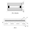
- the liquid crystal grating as illustrated in FIG. 1 is generally composed of an upper polarizer sheet 1 , a lower polarizer sheet 2 , an upper substrate 3 , a lower substrate 4 , and a liquid crystal layer 5 arranged between the two substrates.
- the upper substrate 3 and the lower substrate 4 comprise a plate electrode 6 and strip electrodes 7 respectively, and the plurality of electrode strips of the strip electrodes 7 are arranged parallel to each other.
- the working principle for this liquid crystal grating is described as follows.
- the vibration direction of the polarized light varies gradually when passing though the rotated liquid crystal molecules, and upon reaching the upper polarizing plate 1 , the vibration direction of the polarized light becomes inconsistent with the transmission axle of the upper polarizing plate 1 , such that the light with changed vibration direction can not pass through the upper polarizing plate 1 , and therefore dark strips are thereby formed in the zones corresponding to the strip electrodes.
- the vibration direction of the polarized light does not vary when passing though non-rotated liquid crystal molecules, and upon reaching the upper polarizing plate 1 , the vibration direction of the polarized light is consistent with the transmission axle of the upper polarizing plate 1 , such that the light with unchanged vibration direction can pass through the upper polarizing plate 1 , bright strips are thereby formed in the zones corresponding to parts other than the strip electrodes. In this way, a parallax grating in an extending direction along the length of the strip electrodes is formed, thus achieving a grating three-dimensional display mode.
- the parallax grating is controlled to allow that the light emitted from the pixels corresponding to left eye pictures can only enter a left eye while the light emitted from the pixels corresponding to right eye pictures can only enter a right eye, which makes it possible for the left and right eyes to catch pictures different from each other and thus achieves a three-dimensional display effect.
- Embodiments of the present invention provide a touch naked-eye 3D grating and a display device, and the configuration of such a touch naked-eye 3D grating is relatively simple and is capable of achieving touch function and three-dimensional display function simultaneously.
- An embodiment of the present invention provides a touch naked-eye 3D grating, comprising an upper substrate, a lower substrate located oppositely to the upper substrate, strip electrodes arranged at a side of the lower substrate facing the upper substrate, and a plate electrode arranged at a side of the upper substrate facing the lower substrate, a touch electrode structure located between the upper substrate and the plate electrode, and the touch electrode structure and the plate electrode are insulated from each other.
- the touch electrode structure particularly comprises a plurality of first touch sense lines and a plurality of second touch sense lines arranged to intersect with and insulated from each other, and a touch electrode arranged within an area defined between adjacent two first touch sense lines and adjacent two second touch sense lines; and each of the touch electrodes is electrically connected to adjacent one first touch sense line as well as adjacent one second touch sense line, respectively.
- An embodiment of the present invention also provides a display device comprising a display panel and a touch naked-eye 3D grating located at an emitting side of the display panel, and the touch naked-eye 3D grating is above touch naked-eye 3D grating provided by the embodiment of the present invention.
- FIG. 1 is a structural representation of the liquid crystal grating in conventional art
- FIG. 2 is a structural representation of the touch naked-eye 3D grating provided by an embodiment of the present invention
- FIG. 3 is a structural representation of the touch electrode structure in the touch naked-eye 3D grating provided by an embodiment of the present invention
- FIG. 4 is a schematic cross section along the line A-A in FIG. 3 ;
- FIG. 5 is a schematic cross section along the line B-B in FIG. 3 ;
- FIG. 6 is a schematic view of the display device according to an embodiment of the present invention.
- An embodiment of the present invention provides a touch naked-eye 3D grating, as illustrated in FIG. 2 , comprising an upper substrate 01 , a lower substrate 02 arranged oppositely to the upper substrate 01 , strip electrodes 04 arranged at a side of the lower substrate 02 facing the upper substrate 01 , and a plate electrode 05 arranged at a side of the upper substrate 01 facing the lower substrate 02 .
- the strip electrodes 04 comprise a plurality of electrode strips spaced in a certain interval (slit) and parallel with each other, and FIG. 2 shows a schematic section view of these electrode strips.
- the touch naked-eye 3D grating further comprises a touch electrode structure 06 provided between the upper substrate 01 and the plate electrode 05 , and the touch electrode structure 06 and the plate electrode 05 are insulated from each other.
- One example of the touch electrode structure 06 comprises a plurality of first touch sense lines 061 , a plurality of second touch sense lines 062 , and a touch electrode 063 arranged within an area defined between adjacent two first touch sense lines 061 and adjacent two second touch sense lines 062 , and the first and second touch sense lines are arranged to intersect with and insulated from each other.
- Each of the touch electrodes 063 is electrically connected to adjacent one first touch sense line 061 as well as adjacent one second touch sense line 062 , respectively.
- the above-described naked-eye 3D grating provided in the present embodiment may be a slit grating or may be a column lens grating, and the both kinds of gratings may be achieved with liquid crystal gratings.
- the following description is made taking a liquid crystal grating as an example, i.e., as illustrated in FIG. 2 , the description is made based on such an example in which a liquid crystal layer 03 is provided between the upper substrate 01 and the lower substrate 02 .
- the embodiments of the present invention are also available for the gratings made from an electrochromic material or the like material, and detailed explanation thereof is omitted here.
- the above naked-eye 3D grating provided in the present embodiment may be obtained by adding the touch electrode structure 06 insulated from the plate electrode 05 in a conventional naked-eye 3D grating.
- Each touch electrode 063 in the touch electrode structure 06 creates a capacitor with the plate electrode 05 .
- the finger and a touch electrode 063 also forms a capacitor and such a capacitor can cause a quantity variation of electric charges of the touch electrode 063 . It's thus possible to determine the position of the touching point(s) so as to achieve touch function by detecting signal changes on the first touch sense lines 061 and the second touch sense lines 062 electrically connected with the touch electrode.
- the naked-eye 3D grating provided by this embodiment only need to incorporate a touch electrode structure in the upper substrate, thus simplifying the assembly configuration as well as its production process, and further reducing the overall costs for manufacturing the assembly while decreasing the thickness of the display.
- the naked-eye 3D grating provided in this embodiment, there always provides uniform slits between the strip electrodes 04 .
- a voltage is applied to the strip electrodes 04 and the plate electrode 05 respectively, and potential difference and thus electric field are caused therebetween, the liquid crystal molecule in the liquid crystal layer 03 corresponding the strip electrodes 04 (for example, immediately above the strip electrode 04 in FIG. 2 ) are subjected to rotation, while other liquid crystal molecules corresponding to the slits keep their original shapes without any rotation.
- the parallax grating can be controlled so that the light emitted from the pixels corresponding to left eye pictures can only enter a left eye while the light emitted from the pixels corresponding to right eye pictures can only enter a right eye, which makes it possible for the left and right eyes to catch pictures different from each other and thus achieves a three-dimensional display effect.
- the extending directions of the first touch sense lines 061 and the second touch sense lines 062 in the touch electrode structure 06 are vertical to each other, and both wires 061 and 062 are insulated from each other.
- the first touch sense lines 061 extend in the vertical direction
- the second touch sense lines 062 extend in the horizontal direction.
- the connection relationship between the first touch sense lines 061 and the second touch sense lines 062 with each of the touch electrodes 063 may be a relationship of one-to-one correspondence, as illustrated in FIG. 3 , that is to say, one touch electrode 063 is electrically connected with one adjacent first touch sense line 061 and one adjacent second touch sense line 062 . In this way, during touch occurs at a touch electrode 063 , signal changes only occurs on the one first touch sense line 061 and the one second touch sense line 062 connected with the touch electrode, which makes it possible to determine the position of the touching point accurately.
- each of the first touch sense lines 061 and each of the second touch sense lines 062 may be directly electrically connected with the corresponding touch electrode 063 , and as illustrated in FIG. 4 , may also connected with the corresponding touch electrode 063 through a wire 064 , while no limitation is made herein.
- first touch sense lines 061 and the second touch sense lines 062 in the touch electrode structure 06 may be arranged in a same layer, and bridging structures are used at the crossover locations between the wires 061 and 062 so as to guarantee mutual insulation therebetween. More specifically, a bridging structure may be arranged at the crossover location of one first touch sense line 061 with one second touch sense line 062 , or a bridging structure 065 may be arranged at the crossover location of one second touch sense line 062 with one first touch sense line 061 , as illustrated in FIG. 5 , no limitation is made herein.
- the first touch sense lines 061 and the second touch sense lines 062 in the touch electrode structure 06 may also be provided in different layers and insulated from each other.
- each first touch sense line 061 and each second touch sense line 062 may be arranged between the touch electrodes 063 and the plate electrode 05 , and it's also possible for each first touch sense line 061 and each second touch sense line 062 to be arranged between the touch electrodes 063 and the upper substrate 01 , no limitation is made herein.
- first touch sense lines 061 and the second touch sense lines 062 in the touch electrode structure 06 may be arranged at either side of the touch electrodes 063 , for example.
- each first touch sense line 061 may be provided between the touch electrodes 063 and the plate electrode 05
- each second touch sense line 062 may be provided between the touch electrodes 063 and the upper substrate 01
- each first touch sense line 061 may be provided between the touch electrodes 063 and the upper substrate 01
- each second touch sense line 062 may be provided between the touch electrodes 063 and the plate electrode 05 , no limitation is made herein.
- an embodiment of the present invention also provides a display device, as illustrated in FIG. 6 , comprising a display panel 100 and a touch naked-eye 3D grating 200 located at the emitting side of the display panel, the touch naked-eye 3D grating is any of the above-described touch naked-eye 3D gratings provided by embodiments of the present invention.
- Implementation of this display device may refer to above embodiments of the touch naked-eye 3D gratings, and repeated description is omitted here.
- the display panel of this display device may be a liquid crystal display (LCD) panel, an organic light emitting display (OLED) panel, a plasma display panel (PDP), a cathode-ray tube (CRT) display or the like, and no restrictions are made herein.
- LCD liquid crystal display
- OLED organic light emitting display
- PDP plasma display panel
- CRT cathode-ray tube
- the embodiment of the present invention provides a touch naked-eye 3D grating and a display device, in which a touch electrode structure is added within the naked-eye 3D grating between the upper substrate and the plate electrode; the touch electrode structure comprises a plurality of first touch sense lines and a plurality of second touch sense lines arranged to intersect with and insulated from each other, and a touch electrode arranged within an zone defined between adjacent two first touch sense lines and adjacent two second touch sense lines, and each touch electrode and the plate electrode creates a capacitor.
- touch occurs, the electric field of human body causes quantity variation of electricity on the touch electrode; and by detecting signal changes on the first touch sense line and the second touch sense line electrically connected with the touch electrode, the touch function is achieved.
- the embodiment of the present invention only need to add a touch electrode structure in the upper substrate, thus simplifying the assembly configuration as well as its production process, and further reducing the overall costs for manufacturing the assembly while decreasing the thickness of the display.
Landscapes
- Engineering & Computer Science (AREA)
- Physics & Mathematics (AREA)
- General Engineering & Computer Science (AREA)
- Theoretical Computer Science (AREA)
- General Physics & Mathematics (AREA)
- Human Computer Interaction (AREA)
- Optics & Photonics (AREA)
- Devices For Indicating Variable Information By Combining Individual Elements (AREA)
- Position Input By Displaying (AREA)
- Liquid Crystal (AREA)
Applications Claiming Priority (4)
| Application Number | Priority Date | Filing Date | Title |
|---|---|---|---|
| CN201310199291 | 2013-05-24 | ||
| CN201310199291.7A CN103324001B (zh) | 2013-05-24 | 2013-05-24 | 一种触摸式裸眼3d光栅及显示装置 |
| CN201310199291.7 | 2013-05-24 | ||
| PCT/CN2013/082296 WO2014187041A1 (zh) | 2013-05-24 | 2013-08-26 | 触摸式裸眼3d光栅及显示装置 |
Publications (2)
| Publication Number | Publication Date |
|---|---|
| US20150138136A1 US20150138136A1 (en) | 2015-05-21 |
| US9830007B2 true US9830007B2 (en) | 2017-11-28 |
Family
ID=49192840
Family Applications (1)
| Application Number | Title | Priority Date | Filing Date |
|---|---|---|---|
| US14/348,169 Active 2033-10-26 US9830007B2 (en) | 2013-05-24 | 2013-08-26 | Touch naked-eye 3D grating and display device |
Country Status (3)
| Country | Link |
|---|---|
| US (1) | US9830007B2 (zh) |
| CN (1) | CN103324001B (zh) |
| WO (1) | WO2014187041A1 (zh) |
Families Citing this family (2)
| Publication number | Priority date | Publication date | Assignee | Title |
|---|---|---|---|---|
| CN104503166B (zh) * | 2014-12-30 | 2017-08-18 | 深圳市华星光电技术有限公司 | 裸眼三维触控显示装置的透镜层及其电极结构 |
| CN104834103B (zh) | 2015-05-25 | 2017-04-12 | 京东方科技集团股份有限公司 | 3d光栅、彩膜基板、显示装置及其控制方法 |
Citations (19)
| Publication number | Priority date | Publication date | Assignee | Title |
|---|---|---|---|---|
| CN2927175Y (zh) | 2006-02-13 | 2007-07-25 | 陈其良 | 网格式触控屏 |
| US20070216637A1 (en) * | 2006-03-16 | 2007-09-20 | Tomoyuki Ito | Electro-optical device and electronic apparatus |
| US20090050376A1 (en) * | 2007-08-21 | 2009-02-26 | Jin Jeon | Method of detecting a touch position and touch panel for performing the same |
| CN101976139A (zh) | 2010-08-30 | 2011-02-16 | 华映视讯(吴江)有限公司 | 具有侦测多点触控功能的触控面板及侦测多点触控的方法 |
| US20110109622A1 (en) * | 2009-11-12 | 2011-05-12 | Jung-Eun Son | Stereoscopic liquid crystal display device having touch panel and method for manufacturing the same |
| CN202142042U (zh) | 2011-03-21 | 2012-02-08 | 宸鸿光电科技股份有限公司 | 触控感测装置 |
| CN102629011A (zh) | 2012-04-27 | 2012-08-08 | 华映光电股份有限公司 | 触控立体显示装置 |
| US20120242615A1 (en) * | 2011-03-22 | 2012-09-27 | Sony Corporation | Display device and electronic apparatus |
| CN202735996U (zh) | 2012-08-10 | 2013-02-13 | 北京京东方光电科技有限公司 | 一种3d触摸显示器 |
| CN202854758U (zh) * | 2012-08-27 | 2013-04-03 | 凌巨科技股份有限公司 | 主动式触控显示装置 |
| CN103049148A (zh) | 2011-10-17 | 2013-04-17 | 瑞鼎科技股份有限公司 | 电容式触控显示装置 |
| US20130148043A1 (en) * | 2011-12-13 | 2013-06-13 | Japan Display West, Inc. | Liquid crystal display device, electronic apparatus, and optical device |
| US20130154977A1 (en) * | 2011-12-15 | 2013-06-20 | Lg Display Co., Ltd. | Liquid crystal display device having touch and three-dimensional display functions and method for manufacturing the same |
| US20130215076A1 (en) * | 2012-02-21 | 2013-08-22 | Il Ho Lee | Display apparatus |
| US20130285973A1 (en) * | 2012-04-30 | 2013-10-31 | John Greer Elias | Mitigation of parasitic capacitance |
| US20130335463A1 (en) * | 2012-06-13 | 2013-12-19 | Innolux Corporation | 2d/3d switchable display device and method for manufacturing the same |
| US20140028932A1 (en) * | 2012-07-26 | 2014-01-30 | Hannstar Display Corp. | Display Device Capable of Switching Between a Two-Dimensional Displaying Mode and Three-Dimensional Displaying Mode |
| US20140198268A1 (en) * | 2011-07-29 | 2014-07-17 | Sharp Kabushiki Kaisha | Touch panel substrate and electro-optical device |
| US20140292712A1 (en) * | 2013-03-29 | 2014-10-02 | Japan Display Inc. | Display device with touch detection function, electronic apparatus, and touch detection device |
Family Cites Families (2)
| Publication number | Priority date | Publication date | Assignee | Title |
|---|---|---|---|---|
| KR20120051117A (ko) * | 2010-11-12 | 2012-05-22 | 삼성전자주식회사 | 터치스크린패널 표시장치 |
| TWI456467B (zh) * | 2011-05-20 | 2014-10-11 | Au Optronics Corp | 電容式觸控面板的操作方法及觸控式裸眼立體顯示器 |
-
2013
- 2013-05-24 CN CN201310199291.7A patent/CN103324001B/zh not_active Expired - Fee Related
- 2013-08-26 WO PCT/CN2013/082296 patent/WO2014187041A1/zh active Application Filing
- 2013-08-26 US US14/348,169 patent/US9830007B2/en active Active
Patent Citations (20)
| Publication number | Priority date | Publication date | Assignee | Title |
|---|---|---|---|---|
| CN2927175Y (zh) | 2006-02-13 | 2007-07-25 | 陈其良 | 网格式触控屏 |
| US20070216637A1 (en) * | 2006-03-16 | 2007-09-20 | Tomoyuki Ito | Electro-optical device and electronic apparatus |
| US20090050376A1 (en) * | 2007-08-21 | 2009-02-26 | Jin Jeon | Method of detecting a touch position and touch panel for performing the same |
| US20110109622A1 (en) * | 2009-11-12 | 2011-05-12 | Jung-Eun Son | Stereoscopic liquid crystal display device having touch panel and method for manufacturing the same |
| CN101976139A (zh) | 2010-08-30 | 2011-02-16 | 华映视讯(吴江)有限公司 | 具有侦测多点触控功能的触控面板及侦测多点触控的方法 |
| US20120242612A1 (en) | 2011-03-21 | 2012-09-27 | Ching-Yang Chang | Touch sensing device and scanning method thereof |
| CN202142042U (zh) | 2011-03-21 | 2012-02-08 | 宸鸿光电科技股份有限公司 | 触控感测装置 |
| US20120242615A1 (en) * | 2011-03-22 | 2012-09-27 | Sony Corporation | Display device and electronic apparatus |
| US20140198268A1 (en) * | 2011-07-29 | 2014-07-17 | Sharp Kabushiki Kaisha | Touch panel substrate and electro-optical device |
| CN103049148A (zh) | 2011-10-17 | 2013-04-17 | 瑞鼎科技股份有限公司 | 电容式触控显示装置 |
| US20130148043A1 (en) * | 2011-12-13 | 2013-06-13 | Japan Display West, Inc. | Liquid crystal display device, electronic apparatus, and optical device |
| US20130154977A1 (en) * | 2011-12-15 | 2013-06-20 | Lg Display Co., Ltd. | Liquid crystal display device having touch and three-dimensional display functions and method for manufacturing the same |
| US20130215076A1 (en) * | 2012-02-21 | 2013-08-22 | Il Ho Lee | Display apparatus |
| CN102629011A (zh) | 2012-04-27 | 2012-08-08 | 华映光电股份有限公司 | 触控立体显示装置 |
| US20130285973A1 (en) * | 2012-04-30 | 2013-10-31 | John Greer Elias | Mitigation of parasitic capacitance |
| US20130335463A1 (en) * | 2012-06-13 | 2013-12-19 | Innolux Corporation | 2d/3d switchable display device and method for manufacturing the same |
| US20140028932A1 (en) * | 2012-07-26 | 2014-01-30 | Hannstar Display Corp. | Display Device Capable of Switching Between a Two-Dimensional Displaying Mode and Three-Dimensional Displaying Mode |
| CN202735996U (zh) | 2012-08-10 | 2013-02-13 | 北京京东方光电科技有限公司 | 一种3d触摸显示器 |
| CN202854758U (zh) * | 2012-08-27 | 2013-04-03 | 凌巨科技股份有限公司 | 主动式触控显示装置 |
| US20140292712A1 (en) * | 2013-03-29 | 2014-10-02 | Japan Display Inc. | Display device with touch detection function, electronic apparatus, and touch detection device |
Non-Patent Citations (5)
| Title |
|---|
| First Chinese Office Action Appln. No. 201310199291.7; dated Apr. 3, 2015. |
| International Preliminary Report on Patentability dated Nov. 24, 2015; PCT/CN2013/082296. |
| International Search Report dated Jun. 3, 2014; PCT/CN2013/082296. |
| Machine translation of CN 202854758 U, Hsu J et al. * |
| Second Chinese Office Action Appln. No. 201310199291.7; dated Sep. 18, 2015. |
Also Published As
| Publication number | Publication date |
|---|---|
| US20150138136A1 (en) | 2015-05-21 |
| WO2014187041A1 (zh) | 2014-11-27 |
| CN103324001A (zh) | 2013-09-25 |
| CN103324001B (zh) | 2016-03-16 |
Similar Documents
| Publication | Publication Date | Title |
|---|---|---|
| US9195081B2 (en) | Touch liquid crystal grating, 3D touch display device and driving method of touch liquid crystal grating | |
| US9261993B2 (en) | Touch liquid crystal grating, manufacturing method thereof and touch 3D display device | |
| US9495935B2 (en) | Capacitive in-cell touch screen panel having a common electrode layer provided with sensing and driving electrodes | |
| CN113376911B (zh) | 显示面板和显示装置 | |
| CN103116233B (zh) | 一种触摸液晶光栅结构及3d触摸显示装置 | |
| JP5194339B2 (ja) | 液晶表示素子 | |
| US10133082B2 (en) | Three dimensional grating, color filter substrate, display device and control method thereof | |
| WO2016004725A1 (zh) | 触摸式三维光栅及显示装置 | |
| CN102662283B (zh) | 液晶狭缝光栅、立体显示装置及其校正方法 | |
| US10162227B2 (en) | Liquid crystal grating and control method thereof, 3D touch display panel | |
| CN103293726A (zh) | 液晶盒、3d触控显示装置及其控制方法 | |
| US20180232075A1 (en) | Display Device and Driving Method Thereof | |
| US20170192564A1 (en) | In-Cell Touch Panel and Display Device | |
| US10001853B2 (en) | Touch grating cell and touch stereoscopic display device | |
| CN104951123A (zh) | 带传感器的显示装置及传感器装置 | |
| JP2014132300A (ja) | 液晶レンズ素子及び表示装置並びに端末機 | |
| CN104898337A (zh) | 一种阵列基板、显示面板、显示装置及制作方法 | |
| CN102436100B (zh) | 立体显示装置 | |
| CN203241674U (zh) | 一种触摸式裸眼3d光栅及显示装置 | |
| US10795217B2 (en) | Liquid crystal grating and fabrication method thereof, and naked eye 3D display device | |
| CN106154657B (zh) | 一种3d显示装置及其制备方法 | |
| US9535290B2 (en) | Parallax barrier and display device | |
| US9830007B2 (en) | Touch naked-eye 3D grating and display device | |
| US20170277304A1 (en) | Pressure Detection Device, Grating, Display Device and Display Method Thereof | |
| KR101773691B1 (ko) | 3d 패널 및 그 제조방법과 상기 3d 패널을 구비한 3d 디스플레이 장치 |
Legal Events
| Date | Code | Title | Description |
|---|---|---|---|
| AS | Assignment |
Owner name: BEIJING BOE OPTOELECTRONICS TECHNOLOGY CO., LTD., Free format text: ASSIGNMENT OF ASSIGNORS INTEREST;ASSIGNORS:LONG, JUN;LIU, JUNGUO;ZHANG, HONGKUN;AND OTHERS;REEL/FRAME:032571/0551 Effective date: 20140307 Owner name: BOE TECHNOLOGY GROUP CO., LTD., CHINA Free format text: ASSIGNMENT OF ASSIGNORS INTEREST;ASSIGNORS:LONG, JUN;LIU, JUNGUO;ZHANG, HONGKUN;AND OTHERS;REEL/FRAME:032571/0551 Effective date: 20140307 |
|
| STCF | Information on status: patent grant |
Free format text: PATENTED CASE |
|
| MAFP | Maintenance fee payment |
Free format text: PAYMENT OF MAINTENANCE FEE, 4TH YEAR, LARGE ENTITY (ORIGINAL EVENT CODE: M1551); ENTITY STATUS OF PATENT OWNER: LARGE ENTITY Year of fee payment: 4 |