US9748090B2 - Semiconductor manufacturing apparatus and manufacturing method of semiconductor device - Google Patents
Semiconductor manufacturing apparatus and manufacturing method of semiconductor device Download PDFInfo
- Publication number
- US9748090B2 US9748090B2 US14/740,414 US201514740414A US9748090B2 US 9748090 B2 US9748090 B2 US 9748090B2 US 201514740414 A US201514740414 A US 201514740414A US 9748090 B2 US9748090 B2 US 9748090B2
- Authority
- US
- United States
- Prior art keywords
- semiconductor substrate
- cleaner
- target material
- end portion
- polishing target
- Prior art date
- Legal status (The legal status is an assumption and is not a legal conclusion. Google has not performed a legal analysis and makes no representation as to the accuracy of the status listed.)
- Active, expires
Links
Images


Classifications
-
- H01L21/02057—
-
- H—ELECTRICITY
- H10—SEMICONDUCTOR DEVICES; ELECTRIC SOLID-STATE DEVICES NOT OTHERWISE PROVIDED FOR
- H10P—GENERIC PROCESSES OR APPARATUS FOR THE MANUFACTURE OR TREATMENT OF DEVICES COVERED BY CLASS H10
- H10P70/00—Cleaning of wafers, substrates or parts of devices
- H10P70/20—Cleaning during device manufacture
-
- B—PERFORMING OPERATIONS; TRANSPORTING
- B24—GRINDING; POLISHING
- B24B—MACHINES, DEVICES, OR PROCESSES FOR GRINDING OR POLISHING; DRESSING OR CONDITIONING OF ABRADING SURFACES; FEEDING OF GRINDING, POLISHING, OR LAPPING AGENTS
- B24B37/00—Lapping machines or devices; Accessories
- B24B37/11—Lapping tools
- B24B37/20—Lapping pads for working plane surfaces
- B24B37/24—Lapping pads for working plane surfaces characterised by the composition or properties of the pad materials
-
- H01L21/30625—
-
- H01L21/67046—
-
- H—ELECTRICITY
- H10—SEMICONDUCTOR DEVICES; ELECTRIC SOLID-STATE DEVICES NOT OTHERWISE PROVIDED FOR
- H10P—GENERIC PROCESSES OR APPARATUS FOR THE MANUFACTURE OR TREATMENT OF DEVICES COVERED BY CLASS H10
- H10P52/00—Grinding, lapping or polishing of wafers, substrates or parts of devices
- H10P52/40—Chemomechanical polishing [CMP]
- H10P52/402—Chemomechanical polishing [CMP] of semiconductor materials
-
- H—ELECTRICITY
- H10—SEMICONDUCTOR DEVICES; ELECTRIC SOLID-STATE DEVICES NOT OTHERWISE PROVIDED FOR
- H10P—GENERIC PROCESSES OR APPARATUS FOR THE MANUFACTURE OR TREATMENT OF DEVICES COVERED BY CLASS H10
- H10P72/00—Handling or holding of wafers, substrates or devices during manufacture or treatment thereof
- H10P72/04—Apparatus for manufacture or treatment
- H10P72/0402—Apparatus for fluid treatment
- H10P72/0406—Apparatus for fluid treatment for cleaning followed by drying, rinsing, stripping, blasting or the like
- H10P72/0411—Apparatus for fluid treatment for cleaning followed by drying, rinsing, stripping, blasting or the like for wet cleaning or washing
- H10P72/0412—Apparatus for fluid treatment for cleaning followed by drying, rinsing, stripping, blasting or the like for wet cleaning or washing using mainly scrubbing means, e.g. brushes
Definitions
- the embodiments of the present invention relate to a semiconductor manufacturing apparatus and manufacturing method of semiconductor device.
- a CMP (Chemical Mechanical Polishing) method is used to flatten a material layer on a semiconductor substrate.
- the material layer on the semiconductor substrate is polished with an abrasive while slurry is supplied onto the abrasive.
- deposits such as a silicon dioxide film, a silicon nitride film, and amorphous silicon
- the peeled deposits cause particles, which lead to a decrease in the yield.
- the abrasive particles of the slurry are positively charged.
- many of material layers such as silicon and a silicon dioxide film are negatively charged.
- the abrasive particles are thus likely to adhere to the material layer.
- the abrasive particles having adhered to the semiconductor substrate are conventionally removed by scrub cleaning with PVA (Polyvinyl Acetate) after the CMP.
- PVA Polyvinyl Acetate
- the abrasive particles are likely to remain at end portions of the semiconductor substrate (exposed portions of the semiconductor substrate).
- the semiconductor substrate is dried after the scrub cleaning, the abrasive particles remaining on the semiconductor substrate are firmly fixed to the semiconductor substrate and become harder to be removed. Therefore, even when the scrub cleaning is performed, the problem of the particles caused by the deposits still occurs.
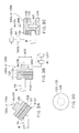
- FIGS. 1A and 1B show a configuration example of a polisher 1 of a CMP apparatus according to a first embodiment
- FIGS. 2A and 2B show a configuration example of a washer 2 in the CMP apparatus according to the first embodiment
- FIGS. 3A to 3C are cross-sectional views showing examples of a configuration of the end portion cleaners 120 a and 120 b according to the first embodiment, respectively;
- FIG. 3D is a top view of the end portion cleaner 120 a or 120 b ;
- FIG. 4 is a flowchart showing an example of a manufacturing method of a semiconductor device using the CMP apparatus according to the first embodiment.
- a semiconductor manufacturing apparatus includes a first cleaner and a second cleaner.
- the first cleaner polishes a semiconductor substrate or a polishing target material on the semiconductor substrate with an abrasive and then cleans a top face of the semiconductor substrate or of the polishing target material while the semiconductor substrate is rotated.
- the second cleaner rubs an end portion of the semiconductor substrate with a physical contact according to rotation of the semiconductor substrate.
- FIGS. 1A and 1B show a configuration example of a polisher 1 of a CMP apparatus according to a first embodiment.
- FIG. 1A is a top view of the polisher 1 and
- FIG. 1B is a side view of the polisher 1 .
- the polisher 1 includes a platen 10 , a polishing pad 20 , a wafer carrier 30 , a slurry supplier 40 , and a pad conditioner 50 .
- the polishing pad 20 is provided on the platen 10 .
- the polishing pad 20 can rotate (rotate around its own axis) together with the platen 10 on the center of the platen 10 as an axis as shown by an arrow A 1 .
- the polishing pad 20 polishes a semiconductor substrate W or a polishing target material on the semiconductor substrate W at a surface of the polishing pad 20 . While the following explanations are given assuming that the polishing pad 20 polishes a polishing target material, the polishing target material can be the semiconductor substrate W itself.
- the wafer carrier 30 holds the semiconductor substrate W and presses the polishing target material against the polishing pad 20 .
- the wafer carrier 30 can rotate on the center of the wafer carrier 30 as an axis as shown by an arrow A 2 .
- the wafer carrier 30 also can move to reciprocate between the center of the polishing pad 20 and an end portion thereof as shown by an arrow A 3 . Accordingly, the wafer carrier 30 can polish the polishing target material at an arbitrary position on the surface of the polishing pad 20 .
- the slurry supplier 40 supplies slurry onto the polishing pad 20 .
- the slurry contains an abrasive and enters between the polishing pad 20 and the polishing target material to polish the polishing target material.
- the wafer carrier 30 rotates the semiconductor substrate W in a direction of the arrow A 2 and also moves the semiconductor substrate W in a direction of the arrow A 3 .
- the polishing target material of the semiconductor substrate W is thus polished.
- the pad conditioner 50 recovers a surface condition of the polishing pad 20 to enable the polishing target material to be polished at as uniform a rate as possible.
- FIGS. 2A and 2B show a configuration example of a washer 2 in the CMP apparatus according to the first embodiment.
- FIG. 2A is a top view of the washer 2 and
- FIG. 2B is a side view of the washer 2 .
- the washer 2 according to the first embodiment can be incorporated in the CMP apparatus together with the polisher 1 shown in FIGS. 1A and 1B or the washer 2 can be provided outside the CMP apparatus separately from the washer 1 .
- the washer 2 includes substrate rotating parts 100 a to 100 d , a scrub cleaner 110 , and end portion cleaners 120 a and 120 b.
- the substrate rotating parts 100 a to 100 d operate to nip end portions of the semiconductor substrate W to rotate the semiconductor substrate W in a direction of an arrow A 12 . More specifically, the substrate rotating parts 100 a to 100 d have trenches TR, respectively, as shown in FIG. 2B and the trenches TR of the substrate rotating parts 100 a to 100 d receive the end portions of the semiconductor substrate W, respectively. The substrate rotating parts 100 a to 100 d thus hold the semiconductor substrate W. The substrate rotating parts 100 a to 100 d rotate on the centers thereof as axes, respectively, as shown by an arrow A 10 in a state of holding the semiconductor substrate W.
- the substrate rotating parts 100 a to 100 d rotate around their own axes, respectively, and forward the semiconductor substrate W in the direction of the arrow A 12 to rotate the semiconductor substrate W on the center of the semiconductor substrate W as an axis.
- the substrate rotating parts 100 a to 100 d are formed of an elastic material not to damage the semiconductor substrate W and, for example, are formed of a urethane resin (polyurethane or urethane rubber).
- the scrub cleaner 110 serving as a first cleaner is formed of an elastic material such as PVA and can rotate on an axis Ax as shown by an arrow A 14 in FIG. 2A in a state of being in contact with the surface of the polishing target material on the semiconductor substrate W.
- the scrub cleaner 110 cleans the top face of the polishing target material while rotating in a direction of the arrow A 14 .
- the semiconductor substrate W rotates in the direction of the arrow A 12 . This removes the abrasive contained in the slurry from the surface of the polishing target material.
- the abrasive particles are likely to remain on exposed portions of the semiconductor substrate W at end portions of the semiconductor substrate W (an outer peripheral area having a width of about 2 millimeters from the outer edge of the semiconductor substrate W, for example) as described above.
- the end portion cleaners 120 a and 120 b serving as a second cleaner are provided in the first embodiment.
- the end portion cleaners 120 a and 120 b physically are in contact with the end portions of the semiconductor substrate W according to the rotation of the semiconductor substrate W and rub the end portions. This enables the abrasive particles remaining on the end portions of the semiconductor substrate W to be removed more reliably.
- the end portion cleaners 120 a and 120 b can be fixed to the cleaner 2 and rub the end portions of the semiconductor substrate W with the rotation of the semiconductor substrate W.
- the end portion cleaners 120 a and 120 b can rub the end portions of the semiconductor substrate W while rotating on the centers of the end portion cleaners 120 a and 120 b as axes, respectively.
- a more specific configuration of the end portion cleaners 120 a and 120 b is explained later with reference to FIGS. 3A to 3D .
- the cleaner 2 further includes a motor M, a current sensor SNS, and a controller CNT.
- the motor M drives the substrate rotating parts 100 a to 100 d , thereby rotating the semiconductor substrate W.
- the current sensor SNS serving as a current measuring part measures a value of the current supplied to the motor M.
- the controller CNT serving as an operating part receives the current value measured by the current sensor SNS and adjusts the current to be supplied to the motor M.
- the controller CNT also detects termination of lives of the end portion cleaners 120 a and 120 b upon reception of the current value measured by the current sensor SNS. Detection of termination of the lives of the end portion cleaners 120 a and 120 b is also explained later.
- FIGS. 3A to 3C are cross-sectional views showing examples of a configuration of the end portion cleaners 120 a and 120 b according to the first embodiment, respectively.
- the end portion cleaners 120 a and 120 b respectively have a stacked structure including a first portion 121 and a second portion 122 .
- the first portion 121 is in contact with an end portion of the semiconductor substrate W and removes the abrasive having adhered to the end portion of the semiconductor substrate W.
- the first portion 121 includes a foamed resin.
- the foamed resin is a resin foamed like a mesh in micron unit and can be a melamine resin.
- a melamine-formaldehyde resin is preferable, for example.
- the melamine resin is excellent in the heat resistance, the water resistance, and the like and also is easily available and low in the cost because it is industrially manufactured in large volume. Chemical binding of such a resin is weaker than that of the semiconductor substrate W or the polishing target material.
- the first portion 121 can remove the abrasive particles having adhered to the end portion of the semiconductor substrate W without using a cleaning agent. Furthermore, because the first portion 121 is scraped while taking the abrasive particles therein, the first portion 121 can rub the end portion of the semiconductor substrate W at an unused portion thereof without being clogged with the abrasive particles.
- the second portion 122 supports the first portion 121 and contains an elastic material softer than the semiconductor substrate W and the polishing target material.
- the second portion 122 is formed of a material different from that of the first portion 121 and is formed of an elastic material such as a polyurethane resin or a nonwoven fabric. Because the second portion 122 is an elastic material, damages on the semiconductor substrate W and the polishing target material can be suppressed even when the first portion 121 is scraped and the second portion 122 is exposed.
- a base 125 supports the second portion 122 .
- a resin or the like harder than the first and second portions 121 and 122 is used for the base 125 . Accordingly, the base 125 can reliably support the first and second portions 121 and 122 .
- the base 125 is fixed to the cleaner 2 in such a manner that a central axis Ax 125 of the base 125 is inclined with respect to the surface of the semiconductor substrate W. Therefore, a contact face F 121 with the semiconductor substrate W in the first portion 121 is in contact with a surface Fw of the semiconductor substrate W to be inclined with respect to the surface Fw.
- the first portion 121 rubs the end portion of the semiconductor substrate W and removes the abrasive particles having adhered to the end portion of the semiconductor substrate W.
- the base 125 is arranged in such a manner that the central axis Ax 125 is substantially parallel to the surface Fw of the semiconductor substrate W. Therefore, the contact face F 121 with the semiconductor substrate W in the first portion 121 is in contact with the surface Fw of the semiconductor substrate W to be substantially perpendicular to the surface Fw.
- the first portion 121 is formed of an elastic material, when the end portion of the semiconductor substrate W is pressed against the first portion 121 , the end portion of the semiconductor substrate W is slightly buried in the first portion 121 and side surfaces and the end portion of the semiconductor substrate W are covered by the first portion 121 .
- the first portion 121 rubs the end portion of the semiconductor substrate W and removes the abrasive particles having adhered to the end portion of the semiconductor substrate W.
- the end portion cleaner 120 a or 120 b shown in FIG. 3B further includes a motor M 1 and a controller CMT 1 .
- the controller CNT 1 controls the motor M 1 and the motor M 1 moves the end portion cleaner 120 a or 120 b in a direction (an arrow A 20 ) substantially perpendicular to the surface Fw of the semiconductor substrate W. Accordingly, the end portion cleaner 120 a or 120 b can move a contact position in the first portion 121 between the contact face F 121 and the semiconductor substrate W.
- the first portion 121 is scraped only at a specific position where the semiconductor substrate W is in contact therewith.
- the second portion 122 is exposed in a short time and the life of the end portion cleaner 120 a or 120 b is shortened.
- the end portion cleaner 120 a or 120 b shown in FIG. 3C further includes a third portion 123 facing the first portion 121 .
- the first portion 121 and the third portion 123 sandwich the end portion of the semiconductor substrate W therebetween.
- the first portion 121 moves in a direction of an arrow A 31 and elastically presses the end portion of the semiconductor substrate W against the third portion 123 .
- the first portion 121 elastically presses the end portion of the semiconductor substrate W using a motor (not shown) or an elastic body (a spring or a rubber, for example).
- the end portion cleaner 120 a or 120 b shown in FIG. 3C further includes a motor M 2 and a controller CNT 2 .
- the controller CNT 2 controls the motor M 2 and the motor M 2 rotates the end portion cleaner 120 a or 120 b on the central axis Ax 125 thereof as an axis as shown by an arrow A 30 .
- the end portion cleaner 120 a or 120 b rotates in a state of sandwiching the end portion of the semiconductor substrate W between the first portion 121 and the third portion 123 .
- the semiconductor substrate W rotates in the direction of the arrow A 12 shown in FIG. 2A .
- the first portion 121 can rub the end portion of the semiconductor substrate W and remove the abrasive particles having adhered to the end portion of the semiconductor substrate W.
- FIG. 3D is a top view of the end portion cleaner 120 a or 120 b .
- the end portion cleaner 120 a or 120 b can be circular in the top view as shown in FIG. 3D .
- the end portion cleaner 120 a or 120 b can have any of the configurations shown in FIGS. 3A to 3C .
- the end portion cleaner 120 a or 120 b has a certain lifetime. For example, when the first portion 121 is scraped and the second portion 122 is exposed, the end portion cleaner 120 a or 120 b needs to be replaced. Detection of such life termination of the end portion cleaner 120 a or 120 b can be achieved by the current sensor SNS and the controller CNT shown in FIG. 2B .
- the controller CNT in FIG. 2B needs to supply a relatively large current to the motor M to keep the rotation rate of the semiconductor substrate W.
- the current sensor SNS is supposed to detect a larger current value after a point of time when the second portion 122 is in contact with the semiconductor substrate W than before the second portion 122 is in contact with the semiconductor substrate W. Therefore, the controller CNT can determine that the second portion 122 is exposed based on a change ratio (an inclination) of the current supplied to the motor M 1 . That is, the controller CNT can detect termination of the life of the end portion cleaner 120 a or 120 b.
- the termination of the life of the end portion cleaner 120 a or 120 b can be detected using the motor M 1 , the controller CNT 1 , and the current sensor SNS 1 shown in FIG. 3B .
- the controller CNT 1 shown in FIG. 3B supplies a relatively large current to the motor M 1 to move the end portion cleaner 120 a or 120 b in the direction of the arrow A 20 .
- the current sensor SNS 1 is thus supposed to detect a larger current after a point of time when the second portion 122 is exposed than before the second portion 122 is exposed. Therefore, the controller CNT 1 can determine that the second portion 122 is exposed based on the current measurement value of the current sensor SNS 1 . That is, the controller CNT 1 can detect the termination of the life of the end portion cleaner 120 a or 120 b.
- the termination of the life of the end portion cleaner 120 a or 120 b can be detected using the motor M 2 , the controller CNT 2 , and the current sensor SNS 2 shown in FIG. 3C .
- the controller CNT 2 shown in FIG. 3C supplies a relatively large current to the motor M 2 to rotate the end portion cleaner 120 a or 120 b in a direction of the arrow A 30 .
- the current sensor SNS 2 is thus supposed to detect a larger current after a point of time when the second portion 122 is exposed than before the second portion 122 is exposed. Therefore, the controller CNT 2 can determine that the second portion 122 is exposed based on the current measurement value of the current sensor SNS 2 . That is, the controller CNT 2 can detect the termination of the life of the end portion cleaner 120 a or 120 b.
- controller CNT, CNT 1 , or CNT 2 outputs an alarm upon detection of the life termination of the end portion cleaner 120 a or 120 b . It suffices that the alarm is output by display on a monitor (not shown) or by issuance of a warning sound from a speaker (not shown).
- the current sensors SNS, SNS 1 , and SNS 2 can be torque sensors.
- the controllers CNT, CNT 1 , and CNT 2 determine whether the second portion 122 is exposed based on torque measurement values from the torque sensors, respectively.
- the end portion cleaners 120 a and 120 b rub the end portions of the semiconductor substrate W with physical contacts according to the rotation of the semiconductor substrate W. This enables the abrasive particles remaining on the end portions of the semiconductor substrate W to be removed more reliably. Because few abrasive particles of the slurry remain on the semiconductor substrate W, it is possible to suppress deposits from adhering onto or around the abrasive particles at the subsequent steps. As a result, occurrence of particles due to the deposits can be suppressed.
- the first portions 121 of the end portion cleaners 120 a and 120 b are foamed like a mesh in micron unit and are scraped while taking the abrasive particles in the mesh. Accordingly, the first portions 121 of the end portion cleaners 120 a and 120 b can remove the abrasive particles having adhered to the end portions of the semiconductor substrate W without using a cleaning agent. Furthermore, the first portions 121 can rub the end portions of the semiconductor substrate W at unused portions without being clogged with the abrasive particles.
- the end portion cleaners 120 a and 120 b respectively have the stacked structure including the first portion 121 and the second portion 122 . Because the second portion 122 is formed of an elastic material, damages of the semiconductor substrate W and the polishing target material can be suppressed even when the second portion 122 is exposed. Furthermore, because the frictional force between the second portion 122 and the semiconductor substrate W is different from that between the first portion 121 and the semiconductor substrate W, the controller CNT, CNT 1 , or CNT 2 can detect the termination of the lives of the end portion cleaners 120 a and 120 b by monitoring a current consumption of the motor M, M 1 , or M 2 .
- FIG. 4 is a flowchart showing an example of a manufacturing method of a semiconductor device using the CMP apparatus according to the first embodiment.
- the polishing target material of the semiconductor substrate W is polished by the CMP method using the polisher 1 shown in FIGS. 1A and 1B (Step S 10 ).
- Step S 20 the surface of the polishing target material of the semiconductor substrate W and the end portions of the semiconductor substrate W are cleaned using the cleaner 2 shown in FIGS. 2A and 2B (Step S 20 ).
- the scrub cleaner 110 cleans the top face of the polishing target material while the semiconductor substrate W is rotated.
- the end portion cleaners 120 a and 120 b rub the end portions of the semiconductor substrate W with physical contacts according to the rotation of the semiconductor substrate W.
- the end portion cleaners 120 a and 120 b can be any one of those shown in FIGS. 3A to 3C .
- the current sensor SNS, SNS 1 , or SNS 2 measures the torque or the current consumption of the motor M, M 1 , or M 2 that rotates the semiconductor substrate W (Step S 22 ).
- the controller CNT, CNT 1 , or CNT 2 determines that the first portion 121 remains and that the second portion 122 is not exposed and then the cleaning at Step S 20 is continued. It suffices that the predetermined threshold is previously stored in a memory in the controller CNT, CNT 1 , or CNT 2 or a memory outside the controller CNT, CNT 1 , or CNT 2 (these memories are not shown).
- the controller CNT, CNT 1 , or CNT 2 determines that the second portion 122 is exposed (Step S 26 ). In this case, the controller CNT, CNT 1 , or CNT 2 displays or issues an alarm to notify an operator of that effect (Step S 27 ).
- the cleaner 2 can stop the cleaning process in this case. The operator can know the termination of the lives of the end portion cleaners 120 a and 120 b and can replace the end portion cleaners 120 a and 120 b at an appropriate moment.
Landscapes
- Engineering & Computer Science (AREA)
- Mechanical Engineering (AREA)
- Mechanical Treatment Of Semiconductor (AREA)
- Cleaning Or Drying Semiconductors (AREA)
- Manufacturing & Machinery (AREA)
Abstract
Description
Claims (17)
Priority Applications (1)
| Application Number | Priority Date | Filing Date | Title |
|---|---|---|---|
| US14/740,414 US9748090B2 (en) | 2015-01-22 | 2015-06-16 | Semiconductor manufacturing apparatus and manufacturing method of semiconductor device |
Applications Claiming Priority (2)
| Application Number | Priority Date | Filing Date | Title |
|---|---|---|---|
| US201562106268P | 2015-01-22 | 2015-01-22 | |
| US14/740,414 US9748090B2 (en) | 2015-01-22 | 2015-06-16 | Semiconductor manufacturing apparatus and manufacturing method of semiconductor device |
Publications (2)
| Publication Number | Publication Date |
|---|---|
| US20160218001A1 US20160218001A1 (en) | 2016-07-28 |
| US9748090B2 true US9748090B2 (en) | 2017-08-29 |
Family
ID=56432797
Family Applications (1)
| Application Number | Title | Priority Date | Filing Date |
|---|---|---|---|
| US14/740,414 Active 2035-11-17 US9748090B2 (en) | 2015-01-22 | 2015-06-16 | Semiconductor manufacturing apparatus and manufacturing method of semiconductor device |
Country Status (1)
| Country | Link |
|---|---|
| US (1) | US9748090B2 (en) |
Cited By (1)
| Publication number | Priority date | Publication date | Assignee | Title |
|---|---|---|---|---|
| US20220293425A1 (en) * | 2021-03-11 | 2022-09-15 | Okamoto Machine Tool Works, Ltd. | Method for manufacturing semiconductor device and apparatus for manufacturing semiconductor device |
Families Citing this family (1)
| Publication number | Priority date | Publication date | Assignee | Title |
|---|---|---|---|---|
| CN116153803B (en) * | 2023-04-23 | 2023-07-14 | 苏州晶睿半导体科技有限公司 | A semiconductor wafer test bench and method with cleaning structure |
Citations (28)
| Publication number | Priority date | Publication date | Assignee | Title |
|---|---|---|---|---|
| JPH0617283Y2 (en) | 1989-04-29 | 1994-05-02 | 日本コロムビア株式会社 | Scrubber washer |
| US5901399A (en) * | 1996-12-30 | 1999-05-11 | Intel Corporation | Flexible-leaf substrate edge cleaning apparatus |
| JP2000021828A (en) | 1998-04-27 | 2000-01-21 | Tokyo Seimitsu Co Ltd | Flattening work device for wafer |
| US6079073A (en) * | 1997-04-01 | 2000-06-27 | Ebara Corporation | Washing installation including plural washers |
| US6167583B1 (en) * | 1997-05-15 | 2001-01-02 | Kabushiki Kaisha Toshiba | Double side cleaning apparatus for semiconductor substrate |
| US6186873B1 (en) * | 2000-04-14 | 2001-02-13 | International Business Machines Corporation | Wafer edge cleaning |
| US6257966B1 (en) | 1998-04-27 | 2001-07-10 | Tokyo Seimitsu Co., Ltd. | Wafer surface machining apparatus |
| JP2001212528A (en) | 2000-02-04 | 2001-08-07 | Dainippon Screen Mfg Co Ltd | Cleaning device |
| US20010051500A1 (en) * | 2000-05-30 | 2001-12-13 | Yoshio Homma | Polishing apparatus |
| US20020023715A1 (en) * | 2000-05-26 | 2002-02-28 | Norio Kimura | Substrate polishing apparatus and substrate polishing mehod |
| US20020031914A1 (en) * | 1999-06-18 | 2002-03-14 | Julia S. Svirchevski | Post-plasma processing wafer cleaning method and system |
| US20020062842A1 (en) * | 1999-06-10 | 2002-05-30 | Katrina A. Mikhaylich | System for cleaning a semiconductor wafer |
| US6733596B1 (en) * | 2002-12-23 | 2004-05-11 | Lam Research Corporation | Substrate cleaning brush preparation sequence, method, and system |
| US6837777B2 (en) * | 2000-03-29 | 2005-01-04 | International Business Machines Corporation | Wafer edge cleaning utilizing polish pad material |
| US20050155629A1 (en) * | 2002-09-30 | 2005-07-21 | Lam Research Corp. | Substrate brush scrubbing and proximity cleaning-drying sequence using compatible chemistries, and method, apparatus, and system for implementing the same |
| US20050229950A1 (en) * | 2004-04-14 | 2005-10-20 | Ming-Chun Chou | Brush positioning device for a wafer cleaning station |
| US20050245171A1 (en) * | 2004-04-28 | 2005-11-03 | Jsr Corporation | Chemical mechanical polishing pad, manufacturing process thereof and chemical mechanical polishing method for semiconductor wafers |
| US20050260942A1 (en) * | 2004-05-24 | 2005-11-24 | Jsr Corporation | Chemical mechanical polishing pad |
| US20060270231A1 (en) * | 2005-05-31 | 2006-11-30 | Texas Instruments Incorporated | Systems and methods for removing wafer edge residue and debris using a residue remover mechanism |
| US20070059935A1 (en) * | 2005-09-06 | 2007-03-15 | Komatsu Electronic Metals Co., Ltd. | Polishing method for semiconductor wafer |
| US20070149096A1 (en) * | 2005-12-28 | 2007-06-28 | Jsr Corporation | Chemical mechanical polishing pad and chemical mechanical polishing method |
| US20080171493A1 (en) * | 2007-01-12 | 2008-07-17 | San Fang Chemical Industry Co., Ltd. | Polishing pad and method of producing the same |
| US20090036033A1 (en) * | 2005-12-09 | 2009-02-05 | Applied Materials, Inc. | Methods and apparatus for processing a substrate |
| US20110177305A1 (en) * | 2010-01-20 | 2011-07-21 | San Fang Chemical Industry Co., Ltd. | Polishing pad and method for making the same |
| US20110248788A1 (en) * | 2009-02-25 | 2011-10-13 | Youichi Fujihira | Glass substrate polishing method, package manufacturing method, piezoelectric vibrator, oscillator, electronic device and radio timepiece |
| US8127395B2 (en) * | 2006-05-05 | 2012-03-06 | Lam Research Corporation | Apparatus for isolated bevel edge clean and method for using the same |
| US20130012107A1 (en) * | 2010-03-25 | 2013-01-10 | Toyo Tire & Rubber Co., Ltd. | Laminate polishing pad |
| US20130048018A1 (en) | 2010-02-22 | 2013-02-28 | Entegris, Inc. | Post-cmp cleaning brush |
-
2015
- 2015-06-16 US US14/740,414 patent/US9748090B2/en active Active
Patent Citations (29)
| Publication number | Priority date | Publication date | Assignee | Title |
|---|---|---|---|---|
| JPH0617283Y2 (en) | 1989-04-29 | 1994-05-02 | 日本コロムビア株式会社 | Scrubber washer |
| US5901399A (en) * | 1996-12-30 | 1999-05-11 | Intel Corporation | Flexible-leaf substrate edge cleaning apparatus |
| US6079073A (en) * | 1997-04-01 | 2000-06-27 | Ebara Corporation | Washing installation including plural washers |
| US6167583B1 (en) * | 1997-05-15 | 2001-01-02 | Kabushiki Kaisha Toshiba | Double side cleaning apparatus for semiconductor substrate |
| US6257966B1 (en) | 1998-04-27 | 2001-07-10 | Tokyo Seimitsu Co., Ltd. | Wafer surface machining apparatus |
| JP2000021828A (en) | 1998-04-27 | 2000-01-21 | Tokyo Seimitsu Co Ltd | Flattening work device for wafer |
| US20020062842A1 (en) * | 1999-06-10 | 2002-05-30 | Katrina A. Mikhaylich | System for cleaning a semiconductor wafer |
| US20020031914A1 (en) * | 1999-06-18 | 2002-03-14 | Julia S. Svirchevski | Post-plasma processing wafer cleaning method and system |
| JP2001212528A (en) | 2000-02-04 | 2001-08-07 | Dainippon Screen Mfg Co Ltd | Cleaning device |
| US6837777B2 (en) * | 2000-03-29 | 2005-01-04 | International Business Machines Corporation | Wafer edge cleaning utilizing polish pad material |
| US6186873B1 (en) * | 2000-04-14 | 2001-02-13 | International Business Machines Corporation | Wafer edge cleaning |
| US20020023715A1 (en) * | 2000-05-26 | 2002-02-28 | Norio Kimura | Substrate polishing apparatus and substrate polishing mehod |
| US20010051500A1 (en) * | 2000-05-30 | 2001-12-13 | Yoshio Homma | Polishing apparatus |
| US20050155629A1 (en) * | 2002-09-30 | 2005-07-21 | Lam Research Corp. | Substrate brush scrubbing and proximity cleaning-drying sequence using compatible chemistries, and method, apparatus, and system for implementing the same |
| US6733596B1 (en) * | 2002-12-23 | 2004-05-11 | Lam Research Corporation | Substrate cleaning brush preparation sequence, method, and system |
| US20050229950A1 (en) * | 2004-04-14 | 2005-10-20 | Ming-Chun Chou | Brush positioning device for a wafer cleaning station |
| US20050245171A1 (en) * | 2004-04-28 | 2005-11-03 | Jsr Corporation | Chemical mechanical polishing pad, manufacturing process thereof and chemical mechanical polishing method for semiconductor wafers |
| US20050260942A1 (en) * | 2004-05-24 | 2005-11-24 | Jsr Corporation | Chemical mechanical polishing pad |
| US20060270231A1 (en) * | 2005-05-31 | 2006-11-30 | Texas Instruments Incorporated | Systems and methods for removing wafer edge residue and debris using a residue remover mechanism |
| US20070059935A1 (en) * | 2005-09-06 | 2007-03-15 | Komatsu Electronic Metals Co., Ltd. | Polishing method for semiconductor wafer |
| US20090036033A1 (en) * | 2005-12-09 | 2009-02-05 | Applied Materials, Inc. | Methods and apparatus for processing a substrate |
| US20070149096A1 (en) * | 2005-12-28 | 2007-06-28 | Jsr Corporation | Chemical mechanical polishing pad and chemical mechanical polishing method |
| US8127395B2 (en) * | 2006-05-05 | 2012-03-06 | Lam Research Corporation | Apparatus for isolated bevel edge clean and method for using the same |
| US20080171493A1 (en) * | 2007-01-12 | 2008-07-17 | San Fang Chemical Industry Co., Ltd. | Polishing pad and method of producing the same |
| US20110248788A1 (en) * | 2009-02-25 | 2011-10-13 | Youichi Fujihira | Glass substrate polishing method, package manufacturing method, piezoelectric vibrator, oscillator, electronic device and radio timepiece |
| US20110177305A1 (en) * | 2010-01-20 | 2011-07-21 | San Fang Chemical Industry Co., Ltd. | Polishing pad and method for making the same |
| US20130048018A1 (en) | 2010-02-22 | 2013-02-28 | Entegris, Inc. | Post-cmp cleaning brush |
| JP2013520803A (en) | 2010-02-22 | 2013-06-06 | インテグリス・インコーポレーテッド | Cleaning brush after CMP |
| US20130012107A1 (en) * | 2010-03-25 | 2013-01-10 | Toyo Tire & Rubber Co., Ltd. | Laminate polishing pad |
Cited By (2)
| Publication number | Priority date | Publication date | Assignee | Title |
|---|---|---|---|---|
| US20220293425A1 (en) * | 2021-03-11 | 2022-09-15 | Okamoto Machine Tool Works, Ltd. | Method for manufacturing semiconductor device and apparatus for manufacturing semiconductor device |
| US12068165B2 (en) * | 2021-03-11 | 2024-08-20 | Okamoto Machine Tool Works, Ltd. | Method for manufacturing semiconductor device and apparatus for manufacturing semiconductor device |
Also Published As
| Publication number | Publication date |
|---|---|
| US20160218001A1 (en) | 2016-07-28 |
Similar Documents
| Publication | Publication Date | Title |
|---|---|---|
| JP6145334B2 (en) | Substrate processing equipment | |
| US9144878B2 (en) | Polishing apparatus and wear detection method | |
| US9403254B2 (en) | Methods for real-time error detection in CMP processing | |
| KR20030043697A (en) | Method of manufacturing semiconductor device and polishing device | |
| US10800000B2 (en) | Multi-layered nano-fibrous CMP pads | |
| US10256120B2 (en) | Systems, methods and apparatus for post-chemical mechanical planarization substrate buff pre-cleaning | |
| US20080223402A1 (en) | Disk-shaped substrate manufacturing method and washing apparatus | |
| US11694909B2 (en) | Brush cleaning apparatus, chemical-mechanical polishing (CMP) system and wafer processing method | |
| KR20140099191A (en) | Method of polishing back surface of substrate and substrate processing apparatus | |
| US20130196572A1 (en) | Conditioning a pad in a cleaning module | |
| US9748090B2 (en) | Semiconductor manufacturing apparatus and manufacturing method of semiconductor device | |
| CN106233432B (en) | System, method and apparatus for substrate cleaning after chemical mechanical planarization | |
| CN105659361B (en) | The grinding method of chip and the grinding device of chip | |
| US8313359B2 (en) | Chemical mechanical polishing apparatus | |
| JP6418790B2 (en) | Cleaning device | |
| US20070212976A1 (en) | Smart polishing media assembly for planarizing substrates | |
| US8821746B2 (en) | Fabrication method of semiconductor device and chemical mechanical polishing apparatus | |
| JP2002361564A (en) | Polishing sheet and method of manufacturing the polishing sheet | |
| CN117444852A (en) | Grinding pad detection method and device, double-sided polishing equipment | |
| US9266213B2 (en) | Method of polishing one side of wafer and single side polishing apparatus for wafer | |
| KR20080086014A (en) | Chemical mechanical polishing equipment | |
| KR20070069846A (en) | Pad Conditioning Equipment for Chemical Mechanical Polishing System | |
| CN120715799A (en) | Grinding equipment and grinding method | |
| TW202604680A (en) | Polishing apparatus monitoring system |
Legal Events
| Date | Code | Title | Description |
|---|---|---|---|
| AS | Assignment |
Owner name: KABUSHIKI KAISHA TOSHIBA, JAPAN Free format text: ASSIGNMENT OF ASSIGNORS INTEREST;ASSIGNORS:HIRASAWA, SHINICHI;FUKUSHIMA, DAI;REEL/FRAME:035843/0649 Effective date: 20150608 |
|
| AS | Assignment |
Owner name: TOSHIBA MEMORY CORPORATION, JAPAN Free format text: ASSIGNMENT OF ASSIGNORS INTEREST;ASSIGNOR:KABUSHIKI KAISHA TOSHIBA;REEL/FRAME:043052/0218 Effective date: 20170614 |
|
| STCF | Information on status: patent grant |
Free format text: PATENTED CASE |
|
| MAFP | Maintenance fee payment |
Free format text: PAYMENT OF MAINTENANCE FEE, 4TH YEAR, LARGE ENTITY (ORIGINAL EVENT CODE: M1551); ENTITY STATUS OF PATENT OWNER: LARGE ENTITY Year of fee payment: 4 |
|
| AS | Assignment |
Owner name: K.K. PANGEA, JAPAN Free format text: MERGER;ASSIGNOR:TOSHIBA MEMORY CORPORATION;REEL/FRAME:055659/0471 Effective date: 20180801 Owner name: TOSHIBA MEMORY CORPORATION, JAPAN Free format text: CHANGE OF NAME AND ADDRESS;ASSIGNOR:K.K. PANGEA;REEL/FRAME:055669/0401 Effective date: 20180801 Owner name: KIOXIA CORPORATION, JAPAN Free format text: CHANGE OF NAME AND ADDRESS;ASSIGNOR:TOSHIBA MEMORY CORPORATION;REEL/FRAME:055669/0001 Effective date: 20191001 |
|
| MAFP | Maintenance fee payment |
Free format text: PAYMENT OF MAINTENANCE FEE, 8TH YEAR, LARGE ENTITY (ORIGINAL EVENT CODE: M1552); ENTITY STATUS OF PATENT OWNER: LARGE ENTITY Year of fee payment: 8 |