US9696489B2 - Semiconductor device and manufacturing method thereof - Google Patents
Semiconductor device and manufacturing method thereof Download PDFInfo
- Publication number
- US9696489B2 US9696489B2 US15/062,153 US201615062153A US9696489B2 US 9696489 B2 US9696489 B2 US 9696489B2 US 201615062153 A US201615062153 A US 201615062153A US 9696489 B2 US9696489 B2 US 9696489B2
- Authority
- US
- United States
- Prior art keywords
- insulating film
- semiconductor
- layer
- optical
- semiconductor device
- Prior art date
- Legal status (The legal status is an assumption and is not a legal conclusion. Google has not performed a legal analysis and makes no representation as to the accuracy of the status listed.)
- Active
Links
Images




Classifications
-
- H—ELECTRICITY
- H10—SEMICONDUCTOR DEVICES; ELECTRIC SOLID-STATE DEVICES NOT OTHERWISE PROVIDED FOR
- H10F—INORGANIC SEMICONDUCTOR DEVICES SENSITIVE TO INFRARED RADIATION, LIGHT, ELECTROMAGNETIC RADIATION OF SHORTER WAVELENGTH OR CORPUSCULAR RADIATION
- H10F71/00—Manufacture or treatment of devices covered by this subclass
-
- G—PHYSICS
- G02—OPTICS
- G02B—OPTICAL ELEMENTS, SYSTEMS OR APPARATUS
- G02B6/00—Light guides; Structural details of arrangements comprising light guides and other optical elements, e.g. couplings
- G02B6/10—Light guides; Structural details of arrangements comprising light guides and other optical elements, e.g. couplings of the optical waveguide type
- G02B6/12—Light guides; Structural details of arrangements comprising light guides and other optical elements, e.g. couplings of the optical waveguide type of the integrated circuit kind
- G02B6/122—Basic optical elements, e.g. light-guiding paths
-
- G—PHYSICS
- G02—OPTICS
- G02B—OPTICAL ELEMENTS, SYSTEMS OR APPARATUS
- G02B6/00—Light guides; Structural details of arrangements comprising light guides and other optical elements, e.g. couplings
- G02B6/10—Light guides; Structural details of arrangements comprising light guides and other optical elements, e.g. couplings of the optical waveguide type
- G02B6/12—Light guides; Structural details of arrangements comprising light guides and other optical elements, e.g. couplings of the optical waveguide type of the integrated circuit kind
- G02B6/13—Integrated optical circuits characterised by the manufacturing method
-
- G—PHYSICS
- G02—OPTICS
- G02B—OPTICAL ELEMENTS, SYSTEMS OR APPARATUS
- G02B6/00—Light guides; Structural details of arrangements comprising light guides and other optical elements, e.g. couplings
- G02B6/10—Light guides; Structural details of arrangements comprising light guides and other optical elements, e.g. couplings of the optical waveguide type
- G02B6/12—Light guides; Structural details of arrangements comprising light guides and other optical elements, e.g. couplings of the optical waveguide type of the integrated circuit kind
- G02B6/13—Integrated optical circuits characterised by the manufacturing method
- G02B6/136—Integrated optical circuits characterised by the manufacturing method by etching
-
- G—PHYSICS
- G02—OPTICS
- G02F—OPTICAL DEVICES OR ARRANGEMENTS FOR THE CONTROL OF LIGHT BY MODIFICATION OF THE OPTICAL PROPERTIES OF THE MEDIA OF THE ELEMENTS INVOLVED THEREIN; NON-LINEAR OPTICS; FREQUENCY-CHANGING OF LIGHT; OPTICAL LOGIC ELEMENTS; OPTICAL ANALOGUE/DIGITAL CONVERTERS
- G02F1/00—Devices or arrangements for the control of the intensity, colour, phase, polarisation or direction of light arriving from an independent light source, e.g. switching, gating or modulating; Non-linear optics
- G02F1/01—Devices or arrangements for the control of the intensity, colour, phase, polarisation or direction of light arriving from an independent light source, e.g. switching, gating or modulating; Non-linear optics for the control of the intensity, phase, polarisation or colour
- G02F1/015—Devices or arrangements for the control of the intensity, colour, phase, polarisation or direction of light arriving from an independent light source, e.g. switching, gating or modulating; Non-linear optics for the control of the intensity, phase, polarisation or colour based on semiconductor elements having potential barriers, e.g. having a PN or PIN junction
- G02F1/025—Devices or arrangements for the control of the intensity, colour, phase, polarisation or direction of light arriving from an independent light source, e.g. switching, gating or modulating; Non-linear optics for the control of the intensity, phase, polarisation or colour based on semiconductor elements having potential barriers, e.g. having a PN or PIN junction in an optical waveguide structure
-
- H—ELECTRICITY
- H10—SEMICONDUCTOR DEVICES; ELECTRIC SOLID-STATE DEVICES NOT OTHERWISE PROVIDED FOR
- H10F—INORGANIC SEMICONDUCTOR DEVICES SENSITIVE TO INFRARED RADIATION, LIGHT, ELECTROMAGNETIC RADIATION OF SHORTER WAVELENGTH OR CORPUSCULAR RADIATION
- H10F77/00—Constructional details of devices covered by this subclass
- H10F77/40—Optical elements or arrangements
- H10F77/407—Optical elements or arrangements indirectly associated with the devices
-
- G—PHYSICS
- G02—OPTICS
- G02B—OPTICAL ELEMENTS, SYSTEMS OR APPARATUS
- G02B6/00—Light guides; Structural details of arrangements comprising light guides and other optical elements, e.g. couplings
- G02B6/10—Light guides; Structural details of arrangements comprising light guides and other optical elements, e.g. couplings of the optical waveguide type
- G02B6/12—Light guides; Structural details of arrangements comprising light guides and other optical elements, e.g. couplings of the optical waveguide type of the integrated circuit kind
- G02B6/122—Basic optical elements, e.g. light-guiding paths
- G02B6/1223—Basic optical elements, e.g. light-guiding paths high refractive index type, i.e. high-contrast waveguides
Definitions
- the present invention relates to a semiconductor device and a manufacturing technology thereof, for example, a technology effectively applied to a semiconductor device having various optical devices in a semiconductor chip.
- Patent Document 1 describes an optical semiconductor device including an optical waveguide formed of a part of a semiconductor layer, a first impurity region which is formed in the semiconductor layer on one side of the optical waveguide and to which an impurity of a first conductivity type is introduced and a second impurity region which is formed in the semiconductor layer on the other side of the optical waveguide and to which an impurity of a second conductivity type opposite to the first conductivity type is introduced.
- an optical waveguide made of silicon In an optical waveguide made of silicon, light partially leaks to the outside in the range nearly equal to the wavelength during the propagation through the optical waveguide. In order to reduce the propagation loss due to the leakage of light, the optical waveguide is covered with an insulating film made of silicon oxide around the entire perimeter (in all directions).
- the optical waveguide is covered with an insulating film made of silicon oxide around the entire perimeter (in all directions), the lights propagating through the respective optical waveguides interfere with each other and the propagation loss cannot be reduced if the intervals between adjacent waveguides are narrow.
- the wavelength of the light propagating through the optical waveguide is 1.5 ⁇ m, the intervals between adjacent waveguides cannot be narrowed to less than 2 ⁇ m. This is one of the factors which prevents the high-density integration of the semiconductor device and restricts the size reduction of the semiconductor chip.
- a semiconductor device of an embodiment includes: a semiconductor substrate; an insulating layer formed on the semiconductor substrate and made of silicon oxide; and a semiconductor layer formed on the insulating layer and made of silicon, and the semiconductor layer constitutes an optical waveguide.
- the insulating layer is removed except for a part thereof to have a hollow structure with a cavity, and both sides surfaces of the semiconductor layer constituting the optical waveguide are covered with air.
- a manufacturing method of a semiconductor device of an embodiment includes the steps of: preparing an SOI substrate having a semiconductor substrate, an insulating layer made of silicon oxide and a semiconductor layer made of silicon; processing the semiconductor layer to form a plurality of optical waveguides; filling spaces between the adjacent optical waveguides with a first insulating film made of silicon nitride; and forming a second insulating film made of silicon oxide on the optical waveguides and the first insulating film.
- the method further includes the steps of: forming a hole penetrating through the first insulating film and the second insulating film; forming a third insulating film made of silicon nitride on the second insulating film with an inclusion of side surfaces and a bottom surface of the hole; removing the third insulating film at a bottom surface of the hole; supplying etchant from the hole to etch the insulating layer, thereby forming a cavity in the insulating layer and exposing both side surfaces and lower surfaces of the optical waveguides; and removing the first insulating film and the third insulating film.
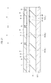
- FIG. 1 is a cross-sectional view showing the principal part of a semiconductor device of the first embodiment
- FIG. 2 is a cross-sectional view showing the principal part of a manufacturing process of a semiconductor device of the first embodiment
- FIG. 3 is a cross-sectional view showing the principal part of the manufacturing process of a semiconductor device continued from FIG. 2 ;
- FIG. 4 is a cross-sectional view showing the principal part of the manufacturing process of a semiconductor device continued from FIG. 3 ;
- FIG. 5A is a cross-sectional view showing the principal part of the manufacturing process of a semiconductor device continued from FIG. 4 ;
- FIG. 5B is a plan view showing the principal part of the manufacturing process of a semiconductor device continued from FIG. 4 ;
- FIG. 6 is a cross-sectional view showing the principal part of the manufacturing process of a semiconductor device continued from FIG. 5 ;
- FIG. 7 is a cross-sectional view showing the principal part of the manufacturing process of a semiconductor device continued from FIG. 6 ;
- FIG. 8 is a cross-sectional view showing the principal part of the manufacturing process of a semiconductor device continued from FIG. 7 ;
- FIG. 9 is a cross-sectional view showing the principal part of the manufacturing process of a semiconductor device continued from FIG. 8 ;
- FIG. 10 is a cross-sectional view showing the principal part of the manufacturing process of a semiconductor device continued from FIG. 9 ;
- FIG. 11 is a cross-sectional view showing the principal part of the manufacturing process of a semiconductor device continued from FIG. 10 ;
- FIG. 12 is a cross-sectional view showing the principal part of a semiconductor device of the second embodiment
- FIG. 13 is a cross-sectional view showing the principal part of a manufacturing process of a semiconductor device of the second embodiment
- FIG. 14 is a cross-sectional view showing the principal part of the manufacturing process of a semiconductor device continued from FIG. 13 ;
- FIG. 15 is a cross-sectional view showing the principal part of the manufacturing process of a semiconductor device continued from FIG. 14 ;
- FIG. 16 is a cross-sectional view showing the principal part of the manufacturing process of a semiconductor device continued from FIG. 15 ;
- FIG. 17 is a cross-sectional view showing the principal part of a semiconductor device of the third embodiment.
- FIG. 18 is a cross-sectional view showing the principal part of a manufacturing process of a semiconductor device of the third embodiment
- FIG. 19 is a cross-sectional view showing the principal part of the manufacturing process of a semiconductor device continued from FIG. 18 ;
- FIG. 20 is a cross-sectional view showing the principal part of the manufacturing process of a semiconductor device continued from FIG. 19 ;
- FIG. 21 is a cross-sectional view showing the principal part of the manufacturing process of a semiconductor device continued from FIG. 20 ;
- FIG. 22 is a cross-sectional view showing the principal part of the manufacturing process of a semiconductor device continued from FIG. 21 ;
- FIG. 23 is a cross-sectional view showing the principal part of the manufacturing process of a semiconductor device continued from FIG. 22 .
- the number of the elements is not limited to a specific number unless otherwise stated or except the case where the number is apparently limited to a specific number in principle, and the number larger or smaller than the specified number is also applicable.
- silicon oxide is represented as SiO 2
- silicon nitride is represented as Si 3 N 4
- silicon oxynitride is represented as SiON, but these include the composition deviated from stoichiometric composition.
- components having the same function are denoted by the same reference characters throughout the drawings for describing the embodiments, and the repetitive description thereof will be omitted.
- the technology disclosed in the first embodiment is applied in particular to an optical device among various devices constituting a semiconductor device using the silicon photonics technology. For this reason, in the following description, a structure and a manufacturing method of a semiconductor device having an optical signal transmission line section and an optical modulation section integrated on an SOI substrate will be described. In addition, in the following description, an optical signal transmission line section and an optical modulation section of the optical device are illustrated as an example and a multilayer wiring with a two-layer structure is illustrated as an example, but the present invention is not limited to these.
- FIG. 1 is a cross-sectional view showing the principal part of a semiconductor device (optical signal transmission line section A and optical modulation section B) of the first embodiment.
- optical devices with a different structure such as a light receiving section and the like are included as described above.
- optical signal line various optical signal transmission lines (referred to also as optical signal line) are formed in the optical signal transmission line section A.
- a rectangular optical waveguide (referred to also as core layer) PO will be described as an example of the optical signal transmission line.
- the optical waveguide PO is constituted of a semiconductor layer (referred to also as SOI layer) SL made of silicon (Si) formed on a semiconductor substrate SUB made of single crystal silicon (Si) with an insulating layer (referred to also as BOX layer or lower cladding layer) CL interposed therebetween.
- a thickness of the insulating layer CL is, for example, 1 ⁇ m or more and less than 2 ⁇ m.
- a preferable range of a thickness of the semiconductor layer SL appears to be, for example, 100 nm to 300 nm (of course not limited to this range depending on other conditions), and a range around a center value of 200 nm appears to be the most preferable range.
- the optical waveguide PO is processed into a plate-like shape and extends in a direction perpendicular to the plane of the paper (z direction shown in FIG. 1 ). Therefore, the optical signal introduced into the optical waveguide PO travels in the direction perpendicular to the plane of the paper.
- a height of the optical waveguide PO (dimension in a longitudinal direction (y direction shown in FIG. 1 )) is, for example, about 200 nm.
- the optical waveguide PO is covered with a first interlayer insulating film (referred to also as upper cladding layer) ID 1 , a second interlayer insulating film ID 2 and a protection film TC.
- the first interlayer insulating film ID 1 and the second interlayer insulating film ID 2 are made of silicon oxide (SiO 2 ) whose refractive index at the wavelength of 1.5 ⁇ m is, for example, about 1.45, and the thickness thereof is, for example, about 1 ⁇ m.
- the protection film TC is made of silicon oxynitride (SiON) whose refractive index at the wavelength of 1.5 ⁇ m is, for example, about 1.82.
- SiON silicon oxynitride
- the optical modulator PC extends in the direction perpendicular to the plane of the paper (z direction shown in FIG. 1 ) and has an optical waveguide (referred to also as core layer) WO formed in a center part thereof when viewed in a lateral direction (x direction shown in FIG. 1 ) orthogonal to the direction perpendicular to the plane of the paper. Therefore, the optical signal introduced into the optical waveguide WO travels in the direction perpendicular to the plane of the paper.
- an optical waveguide referred to also as core layer
- a p type impurity is introduced to form a p type semiconductor PR.
- the p type semiconductor PR is formed to be in parallel to the optical waveguide WO.
- an n type impurity is introduced to form an n type semiconductor NR.
- the n type semiconductor NR is formed to be in parallel to the optical waveguide WO. Namely, the semiconductor layer SL between the p type semiconductor PR and the n type semiconductor NR serves as the optical waveguide WO made of intrinsic semiconductor, so that the pin structure is formed.
- An electrode (first plug PL 1 ) is connected to each of the p type semiconductor PR and the n type semiconductor NR.
- the carrier density in the optical waveguide WO made of intrinsic semiconductor is changed by the voltage applied to the electrode, and a refractive index in the region is changed. Consequently, an effective refractive index to the light propagating through the optical modulator PC is changed, so that an optical phase output from the optical modulator PC can be changed.
- the optical modulator PC is covered with the first interlayer insulating film ID 1 , and connection holes (referred to also as contact hole) CT 1 each reaching the p type semiconductor PR and the n type semiconductor NR are formed in the first interlayer insulating film ID 1 .
- a first plug (referred to also as buried electrode or buried contact) PL 1 made of a material containing tungsten (W) as a main conductive material is formed in the connection hole CT 1 , and the first plug PL 1 electrically connects the p type semiconductor PR and the first-layer wiring M 1 and connects the n type semiconductor NR and the first-layer wiring Ml.
- the first-layer wiring M 1 is made of, for example, a material containing aluminum (Al), copper (Cu) or aluminum-copper alloy (Al-Cu alloy) as a main conductive material.
- the second-layer wiring M 2 is covered with the protection film PC and the protection film. PC is partially opened to expose an upper surface of the second-layer wiring M 2 .
- the insulating layer CL is removed except for a part thereof to have a hollow structure with a cavity. Therefore, the both side surfaces and the lower surface (surface facing toward the semiconductor substrate SUB) of each of the semiconductor layers SL constituting the optical waveguide PO and the optical modulator PC are exposed.
- the difference in refractive index between air and silicon (Si) is larger than that between silicon oxide (SiO 2 ) and silicon (Si).
- the core layer is made of silicon (Si) and the cladding layer is made of silicon oxide (SiO 2 ) is considered.
- the optical confinement effect can be intensified when three surfaces such as both side surfaces and a lower surface of each of the semiconductor layers SL constituting the optical waveguide PO and the optical modulator PC are covered with air in comparison with the case where they are covered with silicon oxide (SiO 2 ).
- the semiconductor layers SL constituting the optical waveguide PO and the optical modulator PC are covered with silicon oxide (SiO 2 ) around the entire perimeter (in all directions). Therefore, the intervals between adjacent semiconductor layers SL, the interval between the semiconductor layer SL and the semiconductor substrate SUB and the interval between the semiconductor layer SL and the first-layer wiring M 1 need to be about 2 to 3 ⁇ m in order to prevent the interference therebetween.
- the intervals between the adjacent semiconductor layers SL are narrowed, the lights propagating through the respective semiconductor layers SL interfere with each other and the propagation loss cannot be reduced.
- the wavelength of the light propagating through the semiconductor layer SL is 1.5 ⁇ m, the intervals between adjacent semiconductor layers SL cannot be reduced to less than 2 ⁇ m. This is one of the factors which prevents the high-density integration of the semiconductor device and restricts the size reduction of the semiconductor chip.
- the first embodiment three surfaces such as both side surfaces and a lower surface of each of the semiconductor layers SL constituting the optical waveguide PO and the optical modulator PC are covered with air, and thus the optical confinement effect can be intensified in comparison with the case where they are covered with silicon oxide (SiO 2 ). Accordingly, the intervals between the adjacent semiconductor layers SL and the interval between the semiconductor layer SL and the semiconductor substrate SUB can be reduced.
- the intervals between the adjacent semiconductor layers SL can be reduced as described above, it is possible to achieve the high-density integration of the semiconductor device and the size reduction of the semiconductor chip. Further, since the interval between the semiconductor layer SL and the semiconductor substrate SUB, that is, the thickness of the insulating layer CL can be reduced to less than 2 ⁇ m, the cost of the SOI substrate can be reduced and the cost reduction of the semiconductor device can be achieved.
- the interval between the adjacent semiconductor layers SL and the interval between the semiconductor layer SL and the semiconductor substrate SUB are desirably set to 1 ⁇ m or more and less than 2 ⁇ m.
- the pattern density of the optical signal transmission line section A and the optical modulation section B is generally low and is, for example, about 5%. Therefore, for example, when the optical waveguide PO and the optical modulator PC are formed by processing the semiconductor layer SL, the phenomenon in which the etching speed differs due to the pattern density (micro-loading effect) occurs.
- the dummy pattern PD made of the semiconductor layer SL is disposed in the region where the optical waveguide PO and the optical modulator PC are not formed. Namely, the insulating film CL is present between the dummy pattern PD and the semiconductor substrate SUB.
- FIG. 2 to FIG. 4 , FIG. 5A and FIG. 6 to FIG. 11 are cross-sectional views showing the principal part of a semiconductor device (for example, optical signal transmission line section A and optical modulation section B) in a manufacturing process of the first embodiment.
- FIG. 5B is a plan view showing the principal part of a semiconductor device (for example, optical signal transmission line section A) in the manufacturing process of the first embodiment.
- the semiconductor layer SL is processed by dry etching using a resist mask, so that the semiconductor layer SL for the optical waveguide is formed in the optical signal transmission line section A and the semiconductor layer SL for the optical modulator is formed in the optical modulation section B.
- the semiconductor layer SL for dummy is also formed in order to suppress the micro-loading effect.
- the optical waveguide PO is formed in the optical signal transmission line section A.
- the optical modulator PC having the pin structure including the optical waveguide WO, the p type semiconductor PR located on one side of the optical waveguide WO and the n type semiconductor NR located on the other side of the optical waveguide WO is formed in the optical modulation section B.
- the dummy pattern PD having a rectangular shape with a side of about 30 to 50 ⁇ m when seen in a plan view is formed. Though not illustrated in FIG. 2 , the dummy pattern PD is arranged around the optical waveguide PO formed in the optical signal transmission line section A and is arranged also around the optical modulator PC formed in the optical modulation section B.
- a first insulating film I 1 and a second insulating film 12 are sequentially formed on an upper surface of the insulating layer CL so as to cover the optical waveguide PO, the optical modulator PC and the dummy pattern PD.
- the first insulating film I 1 is made of, for example, silicon nitride (Si 3 N 4 ) or silicon oxynitride (SiON) and the second insulating film I 2 is made of, for example, silicon oxide (SiO 2 ).
- the first insulating film I 1 is formed to have a thickness larger than that of the semiconductor layer SL and the total thickness of the first insulating film I 1 and the second insulating film I 2 is, for example, about 500 nm.
- a fourth insulating film I 4 is formed on an upper surface of the third insulating film I 3 with the inclusion of side surfaces and bottom surfaces of the holes HL.
- the fourth insulating film I 4 is made of, for example, silicon nitride (Si 3 N 4 ).
- the fourth insulating film I 4 at the bottom surface of each hole HL is removed by, for example, dry etching, and then a part of the insulating layer CL is removed by, for example, wet etching.
- the insulating layer CL located below the optical waveguide PO and the optical modulator PC is removed and the insulating layer CL located below the dummy pattern PD is partially left.
- the lower surface of the optical waveguide PO is completely exposed when the etching of the insulating layer CL stating from the bottom surface of the hole HL proceeds by, for example, 10 ⁇ m.
- the optical modulator PC formed at the position distant from the hole HL by about 5 ⁇ m the lower surface of the optical modulator PC is completely exposed when the etching of the insulating layer CL stating from the bottom surface of the hole HL proceeds by, for example, 10 ⁇ m.
- the lower surface of the dummy pattern PD is not completely exposed because one side of the dummy pattern PD is about 30 to 50 ⁇ m.
- the insulating layer CL is partially left to have the hollow structure with a cavity, so that the lower surfaces of the semiconductor layers SL constituting the optical waveguide PO and the optical modulator PC are exposed.
- a fifth insulating film I 5 is formed on the upper surface of the third insulating film I 3 .
- the fifth insulating film I 5 is made of silicon oxide (SiO 2 ) formed by, for example, plasma CVD and a thickness thereof is, for example, about 500 nm.
- an upper surface of the fifth insulating film 15 is planarized by, for example, CMP, so that the first interlayer insulating film ID 1 made up of the third insulating film I 3 and the fifth insulating film I 5 is formed.
- connection holes CT 1 each reaching the p type semiconductor PR and the n type semiconductor NR of the optical modulator PC are formed in the first interlayer insulating film ID 1 .
- the first plugs PL 1 made of the buried conductive film are formed.
- the first plug PL 1 is made of, for example, aluminum (Al) or tungsten (W).
- a metal film for example, an aluminum (Al) film is deposited on an upper surface of the first interlayer insulating film. ID 1 by, for example, sputtering and the metal film is processed by dry etching using a resist mask, thereby forming the first-layer wiring M 1 .
- Al aluminum
- the second interlayer insulating film ID 2 is formed on the upper surface of the first interlayer insulating film ID 1 so as to cover the first-layer wiring M 1 .
- the second interlayer insulating film ID 2 is made of silicon oxide (SiO 2 ) formed by, for example, plasma CVD and a thickness thereof is, for example, 1 ⁇ m or more.
- an upper surface of the second interlayer insulating film ID 2 is planarized by, for example, CMP and then the connection hole CT 2 reaching the first-layer wiring M 1 is formed in the second interlayer insulating film ID 2 .
- the second plug PL 2 made of the buried conductive film is formed.
- the second plug PL 2 is made of, for example, aluminum (Al) or tungsten (W).
- the cavity is formed in the insulating layer CL and the cavity contains air in the first embodiment.
- an insulating material with a refractive index lower than that of silicon oxide (SiO 2 ) may be injected into the cavity.
- the insulating layer CL may be provided at a part between the optical waveguide PO and the semiconductor substrate SUB and a part between the optical modulator PC and the semiconductor substrate SUB at the position which gives no influence to the optical characteristics.
- the intervals between the adjacent semiconductor layers SL can be reduced to less than 2 ⁇ m in the first embodiment, it is possible to achieve the high-density integration of the semiconductor device and the size reduction of the semiconductor chip. Further, since the interval between the semiconductor layer SL and the semiconductor substrate SUB, that is, the thickness of the insulating layer CL can be reduced to less than 2 ⁇ m, the cost of the SOI substrate can be reduced and the cost reduction of the semiconductor device can be achieved.
- the second embodiment is different from the first embodiment in the shape of the cavity which covers the semiconductor layer SL. Namely, three surfaces such as both side surfaces and a lower surface of each of the semiconductor layers SL constituting the optical waveguide PO and the optical modulator PC are covered with air in the first embodiment, while only both side surfaces of each of the semiconductor layers SL constituting the optical waveguide PO and the optical modulator PC are covered with air and lower surfaces thereof are covered with the insulating layer CL in the second embodiment.
- the semiconductor device of the second embodiment is almost the same as the semiconductor device of the first embodiment described above except for the structure of the cavity and the forming method of the cavity, the difference therebetween will be mainly described below.
- the SOI substrate made up of the semiconductor substrate SUB, the insulating layer CL formed on a main surface of the semiconductor substrate SUB and the semiconductor layer SL formed on an upper surface of the insulating layer CL is used in the semiconductor device, and the semiconductor layer SL constitutes each of the optical waveguide PO in the optical signal transmission line section A and the optical modulator PC in the optical modulation section B.
- the cavity is not formed in the insulating layer CL and only both side surfaces of the semiconductor layers SL constituting the optical waveguide PO and the optical modulator PC are covered with air, and lower surfaces thereof are covered with the insulating layer CL made of, for example, silicon oxide (SiO 2 ).
- the interval between the semiconductor layers SL constituting the optical waveguide PO and the optical modulator PC and the semiconductor substrate SUB is set to, for example, about 2 to 3 ⁇ m.
- FIG. 13 to FIG. 16 are cross-sectional views showing the principal part of a semiconductor device in a manufacturing process of the second embodiment.
- the 501 substrate is prepared and the semiconductor layer SL constituting the SOI substrate is processed to form the optical waveguide PO in the optical signal transmission line section A and the optical modulator PC with the pin structure in the optical modulation section B. Further, the dummy patterns PD are formed around them.
- the insulating layer CL constituting the SOI substrate has the thickness of, for example, about 2 to 3 ⁇ m and is formed to be thicker than the insulating layer CL of the first embodiment described above.
- the upper surface of the second insulating film I 2 is planarized by, for example, CMP and then the upper surface of the first insulating film I 1 is planarized by, for example, CMP until the upper surface of the semiconductor layer SL is exposed. Consequently, the spaces between the adjacent semiconductor layers SL are filled with the first insulating film I 1 .
- each hole HL reaching the first insulating film I 1 is formed in the third insulating film I 3 .
- the diameter of each hole HL is, for example, about 0.5 ⁇ m.
- the holes HL are formed at positions distant from each of the optical waveguide PO and the optical modulator PC by, for example, about 5 ⁇ m when seen in a plan view.
- the fifth insulating film I 5 is formed on the upper surface of the third insulating film I 3 .
- the fifth insulating film I 5 is made of silicon oxide (SiO 2 ) formed by, for example, plasma CVD and the thickness thereof is, for example, about 500 nm.
- the upper surface of the fifth insulating film I 5 is planarized by, for example, CMP, so that the first interlayer insulating film ID 1 made up of the third insulating film I 3 and the fifth insulating film I 5 is formed.
- the protection film TC is formed so as to cover the second-layer wiring M 2 and is then processed to expose the upper surface of the second-layer wiring M 2 . Consequently, the semiconductor device of the second embodiment is almost completed.
- the intervals between the adjacent semiconductor layers SL can be reduced to less than 2 ⁇ m, it is possible to achieve the high-density integration of the semiconductor device and the size reduction of the semiconductor chip.
- the third embodiment is different from the first embodiment in the shape of the cavity which covers the semiconductor layer SL. Namely, three surfaces such as both side surfaces and a lower surface of each of the semiconductor layers SL constituting the optical waveguide PO and the optical modulator PC are covered with air in the first embodiment, while three surfaces such as both side surfaces and an upper surface (surface facing toward a side opposite to the semiconductor substrate SUB) of each of the semiconductor layers SL constituting the optical waveguide PO and the optical modulator PC are covered with air in the third embodiment.
- the semiconductor device of the third embodiment is almost the same as the semiconductor device of the first embodiment described above except for the structure of the cavity and the forming method of the cavity, the difference therebetween will be mainly described below.
- FIG. 17 is a cross-sectional view showing the principal part of the semiconductor device of the third embodiment.
- the cavity is not formed in the insulating layer CL and the cavity is formed in the first-layer insulating film ID 1 .
- the first interlayer insulating film ID 1 is removed except for a part thereof to have a hollow structure with a cavity. Therefore, the both side surfaces and the upper surface of each of the semiconductor layers SL constituting the optical waveguide PO and the optical modulator PC are exposed.
- the lower surfaces of the semiconductor layers SL constituting the optical waveguide PO and the optical modulator PC are covered with the insulating layer CL made of, for example, silicon oxide (SiO 2 ).
- the interval between the semiconductor layers SL and the semiconductor substrate SUB, that is, the thickness of the insulating layer CL is set to, for example, about 2 to 3 ⁇ m.
- the insulating layer CL is not configured to have the hollow structure with a cavity and thus the interval between the semiconductor layer SL and the semiconductor substrate SUB, that is, the thickness of the insulating layer CL cannot be reduced to less than 2 ⁇ m.
- the optical confinement effect can be intensified in comparison with the case where the both side surfaces and the upper surfaces are covered with silicon oxide (SiO 2 ), so that the intervals between the adjacent semiconductor layers SL can be reduced to less than 2 ⁇ m.
- the intervals between the adjacent semiconductor layers SL can be reduced to less than 2 ⁇ m, it is possible to achieve the high-density integration of the semiconductor device and the size reduction of the semiconductor chip.
- a region in which no cavity is formed is present in the first interlayer insulating film ID 1 .
- this region is provided in the region where the dummy pattern PD made of the semiconductor layer SL is formed like in the first embodiment described above.
- the cavity is not formed in the first interlayer insulating film ID 1 also in the region where the first plugs PL 1 which electrically connect the p type semiconductor PR of the optical modulator PC and the first-layer wiring M 1 and connect the n type semiconductor NR and the first-layer wiring M 1 are formed. This region also maintains the cavity formed in the first interlayer insulating film ID 1 .
- FIG. 18 to FIG. 23 are cross-sectional views showing the principal part of a semiconductor device in a manufacturing process of the third embodiment.
- the SOI substrate is prepared and the semiconductor layer SL constituting the SOI substrate is processed to form the optical waveguide PO in the optical signal transmission line section A and the optical modulator PC with the pin structure in the optical modulation section B. Further, the dummy patterns PD are formed around them.
- the insulating layer CL constituting the SOI substrate has the thickness of, for example, about 2 to 3 ⁇ m and is formed to be thicker than the insulating layer CL of the first embodiment described above.
- the first insulating film I 1 and the second insulating film I 2 are sequentially formed on the main surface of the insulating layer CL so as to cover the optical waveguide PO, the optical modulator PC and the dummy pattern PD.
- the first insulating film I 1 is made of, for example, silicon nitride (Si 3 N 4 ) or silicon oxynitride (SiON) and the thickness thereof is, for example, about 50 to 100 nm.
- the second insulating film I 2 is made of, for example, silicon oxide (SiO 2 ) and the thickness thereof is, for example, about 1 ⁇ m.
- a sixth insulating film I 6 and the third insulating film I 3 are sequentially deposited on the upper surface of the second insulating film I 2 .
- the sixth insulating film I 6 is made of, for example, silicon nitride (Si 3 N 4 ) and the thickness thereof is, for example, about 50 to 100 nm.
- the third insulating film I 3 is made of, for example, silicon oxide (SiO 2 ) and the thickness thereof is, for example, about 1 ⁇ m.
- the sixth insulating film I 6 and the fourth insulating film I 4 at the bottom surfaces of the holes HL are removed by, for example, dry etching, and then a part of the second insulating film I 2 is removed by, for example, wet etching.
- the second insulating film I 2 located above the optical waveguide PO and the optical modulator PC with the first insulating film I 1 interposed therebetween is removed.
- the second insulating film I 2 located in the region in which the dummy pattern PD is formed and in apart of the region of the optical modulation section B in which the connection holes CT 1 are to be formed in the subsequent process is partially left.
- the second insulating film I 2 located above the optical waveguide PO is removed when the etching of the second insulating film I 2 stating from the bottom surface of the hole HL proceeds by, for example, 10 ⁇ m.
- the optical modulator PC formed at the position distant from the hole HL by about 5 ⁇ m the second insulating film I 2 located above the optical modulator PC is removed when the etching of the second insulating film I 2 starting from the bottom surface of the hole HL proceeds by, for example, 10 ⁇ m.
- the second insulating film I 2 above the dummy pattern PD is not completely removed and is partially left because one side of the dummy pattern PD is about 30 to 50 ⁇ m.
- the second insulating film I 2 is partially left to have the hollow structure with a cavity.
- the fifth insulating film I 5 is formed on the upper surface of the third insulating film I 3 .
- the fifth insulating film I 5 is made of silicon oxide (SiO 2 ) formed by, for example, plasma CVD and a thickness thereof is, for example, about 500 nm.
- the upper surface of the fifth insulating film I 5 is planarized by, for example, CMP, so that the first interlayer insulating film ID 1 made up of the first insulating film I 1 , the second insulating film I 2 , the third insulating film I 3 , the fifth insulating film I 5 and the sixth insulating film I 6 is formed.
- the first plug PL 1 (not illustrated) is formed in the first interlayer insulating film ID 1 , and the first-layer wiring M 1 electrically connected to the first plug PL 1 is formed. Further, after the second interlayer insulating film ID 2 is formed so as to cover the first-layer wiring M 1 , the second plug PL 2 is formed in the second interlayer insulating film ID 2 and the second-layer wiring M 2 electrically connected to the second plug PL 2 is formed.
- the protection film TC is formed so as to cover the second-layer wiring M 2 and then the protection film TC is processed to expose the upper surface of the second-layer wiring M 2 . Consequently, the semiconductor device of the third embodiment is almost completed.
Landscapes
- Physics & Mathematics (AREA)
- General Physics & Mathematics (AREA)
- Optics & Photonics (AREA)
- Nonlinear Science (AREA)
- Engineering & Computer Science (AREA)
- Microelectronics & Electronic Packaging (AREA)
- Optical Integrated Circuits (AREA)
- Optical Modulation, Optical Deflection, Nonlinear Optics, Optical Demodulation, Optical Logic Elements (AREA)
- Manufacturing & Machinery (AREA)
Priority Applications (1)
| Application Number | Priority Date | Filing Date | Title |
|---|---|---|---|
| US15/606,281 US10038114B2 (en) | 2015-03-24 | 2017-05-26 | Semiconductor device and manufacturing method thereof |
Applications Claiming Priority (2)
| Application Number | Priority Date | Filing Date | Title |
|---|---|---|---|
| JP2015060872A JP2016180860A (ja) | 2015-03-24 | 2015-03-24 | 半導体装置およびその製造方法 |
| JP2015-060872 | 2015-03-24 |
Related Child Applications (1)
| Application Number | Title | Priority Date | Filing Date |
|---|---|---|---|
| US15/606,281 Division US10038114B2 (en) | 2015-03-24 | 2017-05-26 | Semiconductor device and manufacturing method thereof |
Publications (2)
| Publication Number | Publication Date |
|---|---|
| US20160282554A1 US20160282554A1 (en) | 2016-09-29 |
| US9696489B2 true US9696489B2 (en) | 2017-07-04 |
Family
ID=55628865
Family Applications (2)
| Application Number | Title | Priority Date | Filing Date |
|---|---|---|---|
| US15/062,153 Active US9696489B2 (en) | 2015-03-24 | 2016-03-06 | Semiconductor device and manufacturing method thereof |
| US15/606,281 Active US10038114B2 (en) | 2015-03-24 | 2017-05-26 | Semiconductor device and manufacturing method thereof |
Family Applications After (1)
| Application Number | Title | Priority Date | Filing Date |
|---|---|---|---|
| US15/606,281 Active US10038114B2 (en) | 2015-03-24 | 2017-05-26 | Semiconductor device and manufacturing method thereof |
Country Status (6)
| Country | Link |
|---|---|
| US (2) | US9696489B2 (de) |
| EP (1) | EP3073301B1 (de) |
| JP (1) | JP2016180860A (de) |
| KR (1) | KR20160114516A (de) |
| CN (1) | CN106019640A (de) |
| TW (1) | TW201703270A (de) |
Cited By (3)
| Publication number | Priority date | Publication date | Assignee | Title |
|---|---|---|---|---|
| US9885829B2 (en) * | 2015-06-17 | 2018-02-06 | Renesas Electronics Corporation | Semiconductor device and method of manufacturing the same |
| US20180321570A1 (en) * | 2015-12-21 | 2018-11-08 | Wuhan Research Institute Of Posts And Telecommunications | Integrated Electro-Optic Modulator and Method of Improving 3dB Bandwidth Thereof by Means of Substrate Hollowing Out |
| US10921515B2 (en) | 2018-12-12 | 2021-02-16 | Renesas Electronics Corporation | Semiconductor device and method of manufacturing the same |
Families Citing this family (7)
| Publication number | Priority date | Publication date | Assignee | Title |
|---|---|---|---|---|
| JP6412007B2 (ja) * | 2013-10-02 | 2018-10-24 | 技術研究組合光電子融合基盤技術研究所 | 半導体集積回路及びその製造方法 |
| JP6600476B2 (ja) * | 2015-03-30 | 2019-10-30 | ルネサスエレクトロニクス株式会社 | 半導体装置およびその製造方法 |
| JP2018146669A (ja) * | 2017-03-02 | 2018-09-20 | 富士通株式会社 | 光半導体及びその製造方法 |
| US11262500B2 (en) * | 2019-12-02 | 2022-03-01 | Renesas Electronics Corporation | Semiconductor device and including an optical waveguide and method of manufacturing the same |
| DE102020102534A1 (de) * | 2020-01-31 | 2021-08-05 | Gesellschaft für angewandte Mikro- und Optoelektronik mit beschränkter Haftung - AMO GmbH | Halbleitervorrichtung und Halbleitereinrichtung sowie Verfahren zur Herstellung solcher |
| US11764318B2 (en) * | 2020-11-17 | 2023-09-19 | Renesas Electronics Corporation | Semiconductor device and method of manufacturing the same |
| CN117651881B (zh) * | 2021-11-24 | 2025-01-28 | 欧若拉运营公司 | 用于lidar传感器的硅光子设备及制造方法 |
Citations (6)
| Publication number | Priority date | Publication date | Assignee | Title |
|---|---|---|---|---|
| US20020136481A1 (en) | 2001-02-11 | 2002-09-26 | Tony Mule' | Guided-wave optical interconnections embedded within a microelectronic wafer-level batch package |
| US20040017215A1 (en) | 2002-03-19 | 2004-01-29 | Tony Mule | High input/output density optoelectronic probe card for wafer-level test of electrical and optical interconnect components, methods of fabrication, and methods of use |
| US20100247031A1 (en) | 2009-03-25 | 2010-09-30 | Fujitsu Limited | Optical waveguide device, its manufacture method, laser module and optical transmission system |
| JP2012027198A (ja) | 2010-07-22 | 2012-02-09 | Fujitsu Ltd | 光半導体装置及びその製造方法 |
| JP2013041143A (ja) | 2011-08-17 | 2013-02-28 | Fujitsu Ltd | 光半導体装置とその製造方法 |
| US20140291717A1 (en) | 2013-04-02 | 2014-10-02 | Sumitomo Electric Industries, Ltd. | Method for manufacturing mach-zehnder modulator, method for manufacturing optical waveguide, and optical waveguide |
Family Cites Families (5)
| Publication number | Priority date | Publication date | Assignee | Title |
|---|---|---|---|---|
| JPH0738043B2 (ja) * | 1986-09-16 | 1995-04-26 | 日本電信電話株式会社 | シリコン基板上の石英系光導波路 |
| JP4078898B2 (ja) * | 2002-06-28 | 2008-04-23 | 日本電気株式会社 | 熱光学位相シフタ及びその製造方法 |
| JP2013178411A (ja) * | 2012-02-28 | 2013-09-09 | Tohoku Univ | 光カプラースイッチ |
| JP2014149507A (ja) * | 2013-02-04 | 2014-08-21 | Tohoku Univ | 光リング共振器 |
| US9435952B2 (en) * | 2013-06-10 | 2016-09-06 | Freescale Semiconductor, Inc. | Integration of a MEMS beam with optical waveguide and deflection in two dimensions |
-
2015
- 2015-03-24 JP JP2015060872A patent/JP2016180860A/ja not_active Ceased
-
2016
- 2016-03-06 US US15/062,153 patent/US9696489B2/en active Active
- 2016-03-21 TW TW105108612A patent/TW201703270A/zh unknown
- 2016-03-21 KR KR1020160033454A patent/KR20160114516A/ko not_active Withdrawn
- 2016-03-24 CN CN201610172326.1A patent/CN106019640A/zh active Pending
- 2016-03-24 EP EP16162130.5A patent/EP3073301B1/de not_active Not-in-force
-
2017
- 2017-05-26 US US15/606,281 patent/US10038114B2/en active Active
Patent Citations (6)
| Publication number | Priority date | Publication date | Assignee | Title |
|---|---|---|---|---|
| US20020136481A1 (en) | 2001-02-11 | 2002-09-26 | Tony Mule' | Guided-wave optical interconnections embedded within a microelectronic wafer-level batch package |
| US20040017215A1 (en) | 2002-03-19 | 2004-01-29 | Tony Mule | High input/output density optoelectronic probe card for wafer-level test of electrical and optical interconnect components, methods of fabrication, and methods of use |
| US20100247031A1 (en) | 2009-03-25 | 2010-09-30 | Fujitsu Limited | Optical waveguide device, its manufacture method, laser module and optical transmission system |
| JP2012027198A (ja) | 2010-07-22 | 2012-02-09 | Fujitsu Ltd | 光半導体装置及びその製造方法 |
| JP2013041143A (ja) | 2011-08-17 | 2013-02-28 | Fujitsu Ltd | 光半導体装置とその製造方法 |
| US20140291717A1 (en) | 2013-04-02 | 2014-10-02 | Sumitomo Electric Industries, Ltd. | Method for manufacturing mach-zehnder modulator, method for manufacturing optical waveguide, and optical waveguide |
Non-Patent Citations (1)
| Title |
|---|
| Extended European Search Report issued Jul. 27, 2016, in European Patent Application No. EP16162130.5. |
Cited By (4)
| Publication number | Priority date | Publication date | Assignee | Title |
|---|---|---|---|---|
| US9885829B2 (en) * | 2015-06-17 | 2018-02-06 | Renesas Electronics Corporation | Semiconductor device and method of manufacturing the same |
| US10901152B2 (en) | 2015-06-17 | 2021-01-26 | Renesas Electronics Corporation | Semiconductor device and method of manufacturing the same |
| US20180321570A1 (en) * | 2015-12-21 | 2018-11-08 | Wuhan Research Institute Of Posts And Telecommunications | Integrated Electro-Optic Modulator and Method of Improving 3dB Bandwidth Thereof by Means of Substrate Hollowing Out |
| US10921515B2 (en) | 2018-12-12 | 2021-02-16 | Renesas Electronics Corporation | Semiconductor device and method of manufacturing the same |
Also Published As
| Publication number | Publication date |
|---|---|
| US20170263802A1 (en) | 2017-09-14 |
| EP3073301A1 (de) | 2016-09-28 |
| JP2016180860A (ja) | 2016-10-13 |
| EP3073301B1 (de) | 2018-01-03 |
| KR20160114516A (ko) | 2016-10-05 |
| US10038114B2 (en) | 2018-07-31 |
| US20160282554A1 (en) | 2016-09-29 |
| TW201703270A (zh) | 2017-01-16 |
| CN106019640A (zh) | 2016-10-12 |
Similar Documents
| Publication | Publication Date | Title |
|---|---|---|
| US10038114B2 (en) | Semiconductor device and manufacturing method thereof | |
| US9835882B2 (en) | Semiconductor device | |
| US10859765B2 (en) | Optical coupling device and method for manufacturing the same | |
| US10151881B2 (en) | Semiconductor device and manufacturing method of the same | |
| US10746921B2 (en) | Stacked waveguide arrangements providing field confinement | |
| US10267991B2 (en) | Semiconductor device and manufacturing method thereof | |
| KR100723077B1 (ko) | 도파관 구조물 및 그 제조 방법 | |
| US10120129B2 (en) | Semiconductor device and method for manufacturing same | |
| US9508662B2 (en) | Optical semiconductor device | |
| US10401565B2 (en) | Semiconductor device and method of manufacturing the same | |
| US10197822B2 (en) | Semiconductor device and method of manufacturing same | |
| US10002883B2 (en) | Semiconductor device and manufacturing method thereof | |
| US10162110B2 (en) | Semiconductor device and method for manufacturing the same | |
| US10578805B2 (en) | Semiconductor device and manufacturing method thereof | |
| TWI914762B (zh) | 光學裝置及其製造方法 | |
| US20250258338A1 (en) | Optical device and method of manufacture | |
| EP4290285B1 (de) | Verkleidungsstruktur im hinteren ende einer reihe von photonischen chips | |
| CN119493218A (zh) | 半导体结构及其形成方法、硅光器件 | |
| CN120255077A (zh) | 光子集成电路芯片及光子集成电路芯片的制造方法 |
Legal Events
| Date | Code | Title | Description |
|---|---|---|---|
| AS | Assignment |
Owner name: RENESAS ELECTRONICS CORPORATION, JAPAN Free format text: ASSIGNMENT OF ASSIGNORS INTEREST;ASSIGNORS:WATANUKI, SHINICHI;INADA, ATSURO;SIGNING DATES FROM 20160211 TO 20160212;REEL/FRAME:037909/0432 |
|
| STCF | Information on status: patent grant |
Free format text: PATENTED CASE |
|
| MAFP | Maintenance fee payment |
Free format text: PAYMENT OF MAINTENANCE FEE, 4TH YEAR, LARGE ENTITY (ORIGINAL EVENT CODE: M1551); ENTITY STATUS OF PATENT OWNER: LARGE ENTITY Year of fee payment: 4 |
|
| MAFP | Maintenance fee payment |
Free format text: PAYMENT OF MAINTENANCE FEE, 8TH YEAR, LARGE ENTITY (ORIGINAL EVENT CODE: M1552); ENTITY STATUS OF PATENT OWNER: LARGE ENTITY Year of fee payment: 8 |