US9691732B2 - Semiconductor package with elastic coupler and related methods - Google Patents
Semiconductor package with elastic coupler and related methods Download PDFInfo
- Publication number
- US9691732B2 US9691732B2 US15/230,076 US201615230076A US9691732B2 US 9691732 B2 US9691732 B2 US 9691732B2 US 201615230076 A US201615230076 A US 201615230076A US 9691732 B2 US9691732 B2 US 9691732B2
- Authority
- US
- United States
- Prior art keywords
- pin
- substrate
- housing
- spring
- coupled
- Prior art date
- Legal status (The legal status is an assumption and is not a legal conclusion. Google has not performed a legal analysis and makes no representation as to the accuracy of the status listed.)
- Active
Links
Images


Classifications
-
- H—ELECTRICITY
- H01—ELECTRIC ELEMENTS
- H01L—SEMICONDUCTOR DEVICES NOT COVERED BY CLASS H10
- H01L23/00—Details of semiconductor or other solid state devices
- H01L23/02—Containers; Seals
- H01L23/04—Containers; Seals characterised by the shape of the container or parts, e.g. caps, walls
- H01L23/053—Containers; Seals characterised by the shape of the container or parts, e.g. caps, walls the container being a hollow construction and having an insulating or insulated base as a mounting for the semiconductor body
- H01L23/055—Containers; Seals characterised by the shape of the container or parts, e.g. caps, walls the container being a hollow construction and having an insulating or insulated base as a mounting for the semiconductor body the leads having a passage through the base
-
- H—ELECTRICITY
- H01—ELECTRIC ELEMENTS
- H01L—SEMICONDUCTOR DEVICES NOT COVERED BY CLASS H10
- H01L21/00—Processes or apparatus adapted for the manufacture or treatment of semiconductor or solid state devices or of parts thereof
- H01L21/02—Manufacture or treatment of semiconductor devices or of parts thereof
- H01L21/04—Manufacture or treatment of semiconductor devices or of parts thereof the devices having at least one potential-jump barrier or surface barrier, e.g. PN junction, depletion layer or carrier concentration layer
- H01L21/50—Assembly of semiconductor devices using processes or apparatus not provided for in a single one of the subgroups H01L21/06 - H01L21/326, e.g. sealing of a cap to a base of a container
-
- H—ELECTRICITY
- H01—ELECTRIC ELEMENTS
- H01L—SEMICONDUCTOR DEVICES NOT COVERED BY CLASS H10
- H01L23/00—Details of semiconductor or other solid state devices
- H01L23/02—Containers; Seals
- H01L23/04—Containers; Seals characterised by the shape of the container or parts, e.g. caps, walls
- H01L23/041—Containers; Seals characterised by the shape of the container or parts, e.g. caps, walls the container being a hollow construction having no base used as a mounting for the semiconductor body
-
- H—ELECTRICITY
- H01—ELECTRIC ELEMENTS
- H01L—SEMICONDUCTOR DEVICES NOT COVERED BY CLASS H10
- H01L23/00—Details of semiconductor or other solid state devices
- H01L23/02—Containers; Seals
- H01L23/04—Containers; Seals characterised by the shape of the container or parts, e.g. caps, walls
- H01L23/053—Containers; Seals characterised by the shape of the container or parts, e.g. caps, walls the container being a hollow construction and having an insulating or insulated base as a mounting for the semiconductor body
- H01L23/057—Containers; Seals characterised by the shape of the container or parts, e.g. caps, walls the container being a hollow construction and having an insulating or insulated base as a mounting for the semiconductor body the leads being parallel to the base
-
- H—ELECTRICITY
- H01—ELECTRIC ELEMENTS
- H01L—SEMICONDUCTOR DEVICES NOT COVERED BY CLASS H10
- H01L23/00—Details of semiconductor or other solid state devices
- H01L23/02—Containers; Seals
- H01L23/10—Containers; Seals characterised by the material or arrangement of seals between parts, e.g. between cap and base of the container or between leads and walls of the container
-
- H—ELECTRICITY
- H01—ELECTRIC ELEMENTS
- H01L—SEMICONDUCTOR DEVICES NOT COVERED BY CLASS H10
- H01L23/00—Details of semiconductor or other solid state devices
- H01L23/48—Arrangements for conducting electric current to or from the solid state body in operation, e.g. leads, terminal arrangements ; Selection of materials therefor
- H01L23/488—Arrangements for conducting electric current to or from the solid state body in operation, e.g. leads, terminal arrangements ; Selection of materials therefor consisting of soldered or bonded constructions
- H01L23/492—Bases or plates or solder therefor
-
- H—ELECTRICITY
- H01—ELECTRIC ELEMENTS
- H01L—SEMICONDUCTOR DEVICES NOT COVERED BY CLASS H10
- H01L23/00—Details of semiconductor or other solid state devices
- H01L23/48—Arrangements for conducting electric current to or from the solid state body in operation, e.g. leads, terminal arrangements ; Selection of materials therefor
- H01L23/488—Arrangements for conducting electric current to or from the solid state body in operation, e.g. leads, terminal arrangements ; Selection of materials therefor consisting of soldered or bonded constructions
- H01L23/498—Leads, i.e. metallisations or lead-frames on insulating substrates, e.g. chip carriers
- H01L23/49811—Additional leads joined to the metallisation on the insulating substrate, e.g. pins, bumps, wires, flat leads
-
- H—ELECTRICITY
- H01—ELECTRIC ELEMENTS
- H01L—SEMICONDUCTOR DEVICES NOT COVERED BY CLASS H10
- H01L23/00—Details of semiconductor or other solid state devices
- H01L23/48—Arrangements for conducting electric current to or from the solid state body in operation, e.g. leads, terminal arrangements ; Selection of materials therefor
- H01L23/488—Arrangements for conducting electric current to or from the solid state body in operation, e.g. leads, terminal arrangements ; Selection of materials therefor consisting of soldered or bonded constructions
- H01L23/498—Leads, i.e. metallisations or lead-frames on insulating substrates, e.g. chip carriers
- H01L23/49838—Geometry or layout
- H01L23/49844—Geometry or layout for devices being provided for in H01L29/00
-
- H—ELECTRICITY
- H01—ELECTRIC ELEMENTS
- H01L—SEMICONDUCTOR DEVICES NOT COVERED BY CLASS H10
- H01L23/00—Details of semiconductor or other solid state devices
- H01L23/48—Arrangements for conducting electric current to or from the solid state body in operation, e.g. leads, terminal arrangements ; Selection of materials therefor
- H01L23/488—Arrangements for conducting electric current to or from the solid state body in operation, e.g. leads, terminal arrangements ; Selection of materials therefor consisting of soldered or bonded constructions
- H01L23/498—Leads, i.e. metallisations or lead-frames on insulating substrates, e.g. chip carriers
- H01L23/49861—Lead-frames fixed on or encapsulated in insulating substrates
-
- H—ELECTRICITY
- H01—ELECTRIC ELEMENTS
- H01L—SEMICONDUCTOR DEVICES NOT COVERED BY CLASS H10
- H01L23/00—Details of semiconductor or other solid state devices
- H01L23/48—Arrangements for conducting electric current to or from the solid state body in operation, e.g. leads, terminal arrangements ; Selection of materials therefor
- H01L23/50—Arrangements for conducting electric current to or from the solid state body in operation, e.g. leads, terminal arrangements ; Selection of materials therefor for integrated circuit devices, e.g. power bus, number of leads
-
- H—ELECTRICITY
- H01—ELECTRIC ELEMENTS
- H01L—SEMICONDUCTOR DEVICES NOT COVERED BY CLASS H10
- H01L24/00—Arrangements for connecting or disconnecting semiconductor or solid-state bodies; Methods or apparatus related thereto
- H01L24/71—Means for bonding not being attached to, or not being formed on, the surface to be connected
- H01L24/72—Detachable connecting means consisting of mechanical auxiliary parts connecting the device, e.g. pressure contacts using springs or clips
-
- H—ELECTRICITY
- H01—ELECTRIC ELEMENTS
- H01L—SEMICONDUCTOR DEVICES NOT COVERED BY CLASS H10
- H01L25/00—Assemblies consisting of a plurality of individual semiconductor or other solid state devices ; Multistep manufacturing processes thereof
- H01L25/03—Assemblies consisting of a plurality of individual semiconductor or other solid state devices ; Multistep manufacturing processes thereof all the devices being of a type provided for in the same subgroup of groups H01L27/00 - H01L33/00, or in a single subclass of H10K, H10N, e.g. assemblies of rectifier diodes
- H01L25/04—Assemblies consisting of a plurality of individual semiconductor or other solid state devices ; Multistep manufacturing processes thereof all the devices being of a type provided for in the same subgroup of groups H01L27/00 - H01L33/00, or in a single subclass of H10K, H10N, e.g. assemblies of rectifier diodes the devices not having separate containers
- H01L25/07—Assemblies consisting of a plurality of individual semiconductor or other solid state devices ; Multistep manufacturing processes thereof all the devices being of a type provided for in the same subgroup of groups H01L27/00 - H01L33/00, or in a single subclass of H10K, H10N, e.g. assemblies of rectifier diodes the devices not having separate containers the devices being of a type provided for in group H01L29/00
- H01L25/072—Assemblies consisting of a plurality of individual semiconductor or other solid state devices ; Multistep manufacturing processes thereof all the devices being of a type provided for in the same subgroup of groups H01L27/00 - H01L33/00, or in a single subclass of H10K, H10N, e.g. assemblies of rectifier diodes the devices not having separate containers the devices being of a type provided for in group H01L29/00 the devices being arranged next to each other
-
- H—ELECTRICITY
- H01—ELECTRIC ELEMENTS
- H01R—ELECTRICALLY-CONDUCTIVE CONNECTIONS; STRUCTURAL ASSOCIATIONS OF A PLURALITY OF MUTUALLY-INSULATED ELECTRICAL CONNECTING ELEMENTS; COUPLING DEVICES; CURRENT COLLECTORS
- H01R4/00—Electrically-conductive connections between two or more conductive members in direct contact, i.e. touching one another; Means for effecting or maintaining such contact; Electrically-conductive connections having two or more spaced connecting locations for conductors and using contact members penetrating insulation
- H01R4/28—Clamped connections, spring connections
- H01R4/48—Clamped connections, spring connections utilising a spring, clip, or other resilient member
- H01R4/4854—Clamped connections, spring connections utilising a spring, clip, or other resilient member using a wire spring
- H01R4/4863—Coil spring
-
- H—ELECTRICITY
- H01—ELECTRIC ELEMENTS
- H01R—ELECTRICALLY-CONDUCTIVE CONNECTIONS; STRUCTURAL ASSOCIATIONS OF A PLURALITY OF MUTUALLY-INSULATED ELECTRICAL CONNECTING ELEMENTS; COUPLING DEVICES; CURRENT COLLECTORS
- H01R4/00—Electrically-conductive connections between two or more conductive members in direct contact, i.e. touching one another; Means for effecting or maintaining such contact; Electrically-conductive connections having two or more spaced connecting locations for conductors and using contact members penetrating insulation
- H01R4/28—Clamped connections, spring connections
- H01R4/48—Clamped connections, spring connections utilising a spring, clip, or other resilient member
- H01R4/489—Clamped connections, spring connections utilising a spring, clip, or other resilient member spring force increased by screw, cam, wedge, or other fastening means
-
- H—ELECTRICITY
- H01—ELECTRIC ELEMENTS
- H01L—SEMICONDUCTOR DEVICES NOT COVERED BY CLASS H10
- H01L2224/00—Indexing scheme for arrangements for connecting or disconnecting semiconductor or solid-state bodies and methods related thereto as covered by H01L24/00
- H01L2224/01—Means for bonding being attached to, or being formed on, the surface to be connected, e.g. chip-to-package, die-attach, "first-level" interconnects; Manufacturing methods related thereto
- H01L2224/02—Bonding areas; Manufacturing methods related thereto
- H01L2224/04—Structure, shape, material or disposition of the bonding areas prior to the connecting process
- H01L2224/0401—Bonding areas specifically adapted for bump connectors, e.g. under bump metallisation [UBM]
-
- H—ELECTRICITY
- H01—ELECTRIC ELEMENTS
- H01L—SEMICONDUCTOR DEVICES NOT COVERED BY CLASS H10
- H01L2224/00—Indexing scheme for arrangements for connecting or disconnecting semiconductor or solid-state bodies and methods related thereto as covered by H01L24/00
- H01L2224/01—Means for bonding being attached to, or being formed on, the surface to be connected, e.g. chip-to-package, die-attach, "first-level" interconnects; Manufacturing methods related thereto
- H01L2224/02—Bonding areas; Manufacturing methods related thereto
- H01L2224/04—Structure, shape, material or disposition of the bonding areas prior to the connecting process
- H01L2224/04034—Bonding areas specifically adapted for strap connectors
-
- H—ELECTRICITY
- H01—ELECTRIC ELEMENTS
- H01L—SEMICONDUCTOR DEVICES NOT COVERED BY CLASS H10
- H01L2224/00—Indexing scheme for arrangements for connecting or disconnecting semiconductor or solid-state bodies and methods related thereto as covered by H01L24/00
- H01L2224/01—Means for bonding being attached to, or being formed on, the surface to be connected, e.g. chip-to-package, die-attach, "first-level" interconnects; Manufacturing methods related thereto
- H01L2224/02—Bonding areas; Manufacturing methods related thereto
- H01L2224/04—Structure, shape, material or disposition of the bonding areas prior to the connecting process
- H01L2224/04042—Bonding areas specifically adapted for wire connectors, e.g. wirebond pads
-
- H—ELECTRICITY
- H01—ELECTRIC ELEMENTS
- H01L—SEMICONDUCTOR DEVICES NOT COVERED BY CLASS H10
- H01L2224/00—Indexing scheme for arrangements for connecting or disconnecting semiconductor or solid-state bodies and methods related thereto as covered by H01L24/00
- H01L2224/01—Means for bonding being attached to, or being formed on, the surface to be connected, e.g. chip-to-package, die-attach, "first-level" interconnects; Manufacturing methods related thereto
- H01L2224/02—Bonding areas; Manufacturing methods related thereto
- H01L2224/04—Structure, shape, material or disposition of the bonding areas prior to the connecting process
- H01L2224/05—Structure, shape, material or disposition of the bonding areas prior to the connecting process of an individual bonding area
- H01L2224/0554—External layer
- H01L2224/0555—Shape
- H01L2224/05552—Shape in top view
- H01L2224/05553—Shape in top view being rectangular
-
- H—ELECTRICITY
- H01—ELECTRIC ELEMENTS
- H01L—SEMICONDUCTOR DEVICES NOT COVERED BY CLASS H10
- H01L2224/00—Indexing scheme for arrangements for connecting or disconnecting semiconductor or solid-state bodies and methods related thereto as covered by H01L24/00
- H01L2224/01—Means for bonding being attached to, or being formed on, the surface to be connected, e.g. chip-to-package, die-attach, "first-level" interconnects; Manufacturing methods related thereto
- H01L2224/02—Bonding areas; Manufacturing methods related thereto
- H01L2224/04—Structure, shape, material or disposition of the bonding areas prior to the connecting process
- H01L2224/06—Structure, shape, material or disposition of the bonding areas prior to the connecting process of a plurality of bonding areas
- H01L2224/0601—Structure
- H01L2224/0603—Bonding areas having different sizes, e.g. different heights or widths
-
- H—ELECTRICITY
- H01—ELECTRIC ELEMENTS
- H01L—SEMICONDUCTOR DEVICES NOT COVERED BY CLASS H10
- H01L2224/00—Indexing scheme for arrangements for connecting or disconnecting semiconductor or solid-state bodies and methods related thereto as covered by H01L24/00
- H01L2224/01—Means for bonding being attached to, or being formed on, the surface to be connected, e.g. chip-to-package, die-attach, "first-level" interconnects; Manufacturing methods related thereto
- H01L2224/02—Bonding areas; Manufacturing methods related thereto
- H01L2224/04—Structure, shape, material or disposition of the bonding areas prior to the connecting process
- H01L2224/06—Structure, shape, material or disposition of the bonding areas prior to the connecting process of a plurality of bonding areas
- H01L2224/061—Disposition
- H01L2224/0618—Disposition being disposed on at least two different sides of the body, e.g. dual array
- H01L2224/06181—On opposite sides of the body
-
- H—ELECTRICITY
- H01—ELECTRIC ELEMENTS
- H01L—SEMICONDUCTOR DEVICES NOT COVERED BY CLASS H10
- H01L2224/00—Indexing scheme for arrangements for connecting or disconnecting semiconductor or solid-state bodies and methods related thereto as covered by H01L24/00
- H01L2224/01—Means for bonding being attached to, or being formed on, the surface to be connected, e.g. chip-to-package, die-attach, "first-level" interconnects; Manufacturing methods related thereto
- H01L2224/10—Bump connectors; Manufacturing methods related thereto
- H01L2224/15—Structure, shape, material or disposition of the bump connectors after the connecting process
- H01L2224/16—Structure, shape, material or disposition of the bump connectors after the connecting process of an individual bump connector
- H01L2224/161—Disposition
- H01L2224/16151—Disposition the bump connector connecting between a semiconductor or solid-state body and an item not being a semiconductor or solid-state body, e.g. chip-to-substrate, chip-to-passive
- H01L2224/16221—Disposition the bump connector connecting between a semiconductor or solid-state body and an item not being a semiconductor or solid-state body, e.g. chip-to-substrate, chip-to-passive the body and the item being stacked
- H01L2224/16225—Disposition the bump connector connecting between a semiconductor or solid-state body and an item not being a semiconductor or solid-state body, e.g. chip-to-substrate, chip-to-passive the body and the item being stacked the item being non-metallic, e.g. insulating substrate with or without metallisation
- H01L2224/16227—Disposition the bump connector connecting between a semiconductor or solid-state body and an item not being a semiconductor or solid-state body, e.g. chip-to-substrate, chip-to-passive the body and the item being stacked the item being non-metallic, e.g. insulating substrate with or without metallisation the bump connector connecting to a bond pad of the item
-
- H—ELECTRICITY
- H01—ELECTRIC ELEMENTS
- H01L—SEMICONDUCTOR DEVICES NOT COVERED BY CLASS H10
- H01L2224/00—Indexing scheme for arrangements for connecting or disconnecting semiconductor or solid-state bodies and methods related thereto as covered by H01L24/00
- H01L2224/01—Means for bonding being attached to, or being formed on, the surface to be connected, e.g. chip-to-package, die-attach, "first-level" interconnects; Manufacturing methods related thereto
- H01L2224/26—Layer connectors, e.g. plate connectors, solder or adhesive layers; Manufacturing methods related thereto
- H01L2224/31—Structure, shape, material or disposition of the layer connectors after the connecting process
- H01L2224/32—Structure, shape, material or disposition of the layer connectors after the connecting process of an individual layer connector
- H01L2224/321—Disposition
- H01L2224/32151—Disposition the layer connector connecting between a semiconductor or solid-state body and an item not being a semiconductor or solid-state body, e.g. chip-to-substrate, chip-to-passive
- H01L2224/32221—Disposition the layer connector connecting between a semiconductor or solid-state body and an item not being a semiconductor or solid-state body, e.g. chip-to-substrate, chip-to-passive the body and the item being stacked
- H01L2224/32225—Disposition the layer connector connecting between a semiconductor or solid-state body and an item not being a semiconductor or solid-state body, e.g. chip-to-substrate, chip-to-passive the body and the item being stacked the item being non-metallic, e.g. insulating substrate with or without metallisation
-
- H—ELECTRICITY
- H01—ELECTRIC ELEMENTS
- H01L—SEMICONDUCTOR DEVICES NOT COVERED BY CLASS H10
- H01L2224/00—Indexing scheme for arrangements for connecting or disconnecting semiconductor or solid-state bodies and methods related thereto as covered by H01L24/00
- H01L2224/01—Means for bonding being attached to, or being formed on, the surface to be connected, e.g. chip-to-package, die-attach, "first-level" interconnects; Manufacturing methods related thereto
- H01L2224/26—Layer connectors, e.g. plate connectors, solder or adhesive layers; Manufacturing methods related thereto
- H01L2224/31—Structure, shape, material or disposition of the layer connectors after the connecting process
- H01L2224/33—Structure, shape, material or disposition of the layer connectors after the connecting process of a plurality of layer connectors
- H01L2224/331—Disposition
- H01L2224/3318—Disposition being disposed on at least two different sides of the body, e.g. dual array
- H01L2224/33181—On opposite sides of the body
-
- H—ELECTRICITY
- H01—ELECTRIC ELEMENTS
- H01L—SEMICONDUCTOR DEVICES NOT COVERED BY CLASS H10
- H01L2224/00—Indexing scheme for arrangements for connecting or disconnecting semiconductor or solid-state bodies and methods related thereto as covered by H01L24/00
- H01L2224/01—Means for bonding being attached to, or being formed on, the surface to be connected, e.g. chip-to-package, die-attach, "first-level" interconnects; Manufacturing methods related thereto
- H01L2224/34—Strap connectors, e.g. copper straps for grounding power devices; Manufacturing methods related thereto
- H01L2224/39—Structure, shape, material or disposition of the strap connectors after the connecting process
- H01L2224/40—Structure, shape, material or disposition of the strap connectors after the connecting process of an individual strap connector
- H01L2224/401—Disposition
- H01L2224/40135—Connecting between different semiconductor or solid-state bodies, i.e. chip-to-chip
- H01L2224/40137—Connecting between different semiconductor or solid-state bodies, i.e. chip-to-chip the bodies being arranged next to each other, e.g. on a common substrate
- H01L2224/40139—Connecting between different semiconductor or solid-state bodies, i.e. chip-to-chip the bodies being arranged next to each other, e.g. on a common substrate with an intermediate bond, e.g. continuous strap daisy chain
-
- H—ELECTRICITY
- H01—ELECTRIC ELEMENTS
- H01L—SEMICONDUCTOR DEVICES NOT COVERED BY CLASS H10
- H01L2224/00—Indexing scheme for arrangements for connecting or disconnecting semiconductor or solid-state bodies and methods related thereto as covered by H01L24/00
- H01L2224/01—Means for bonding being attached to, or being formed on, the surface to be connected, e.g. chip-to-package, die-attach, "first-level" interconnects; Manufacturing methods related thereto
- H01L2224/34—Strap connectors, e.g. copper straps for grounding power devices; Manufacturing methods related thereto
- H01L2224/39—Structure, shape, material or disposition of the strap connectors after the connecting process
- H01L2224/40—Structure, shape, material or disposition of the strap connectors after the connecting process of an individual strap connector
- H01L2224/401—Disposition
- H01L2224/40151—Connecting between a semiconductor or solid-state body and an item not being a semiconductor or solid-state body, e.g. chip-to-substrate, chip-to-passive
- H01L2224/40221—Connecting between a semiconductor or solid-state body and an item not being a semiconductor or solid-state body, e.g. chip-to-substrate, chip-to-passive the body and the item being stacked
- H01L2224/40225—Connecting between a semiconductor or solid-state body and an item not being a semiconductor or solid-state body, e.g. chip-to-substrate, chip-to-passive the body and the item being stacked the item being non-metallic, e.g. insulating substrate with or without metallisation
-
- H—ELECTRICITY
- H01—ELECTRIC ELEMENTS
- H01L—SEMICONDUCTOR DEVICES NOT COVERED BY CLASS H10
- H01L2224/00—Indexing scheme for arrangements for connecting or disconnecting semiconductor or solid-state bodies and methods related thereto as covered by H01L24/00
- H01L2224/01—Means for bonding being attached to, or being formed on, the surface to be connected, e.g. chip-to-package, die-attach, "first-level" interconnects; Manufacturing methods related thereto
- H01L2224/42—Wire connectors; Manufacturing methods related thereto
- H01L2224/44—Structure, shape, material or disposition of the wire connectors prior to the connecting process
- H01L2224/45—Structure, shape, material or disposition of the wire connectors prior to the connecting process of an individual wire connector
- H01L2224/45001—Core members of the connector
- H01L2224/45099—Material
- H01L2224/451—Material with a principal constituent of the material being a metal or a metalloid, e.g. boron (B), silicon (Si), germanium (Ge), arsenic (As), antimony (Sb), tellurium (Te) and polonium (Po), and alloys thereof
- H01L2224/45117—Material with a principal constituent of the material being a metal or a metalloid, e.g. boron (B), silicon (Si), germanium (Ge), arsenic (As), antimony (Sb), tellurium (Te) and polonium (Po), and alloys thereof the principal constituent melting at a temperature of greater than or equal to 400°C and less than 950°C
- H01L2224/45124—Aluminium (Al) as principal constituent
-
- H—ELECTRICITY
- H01—ELECTRIC ELEMENTS
- H01L—SEMICONDUCTOR DEVICES NOT COVERED BY CLASS H10
- H01L2224/00—Indexing scheme for arrangements for connecting or disconnecting semiconductor or solid-state bodies and methods related thereto as covered by H01L24/00
- H01L2224/01—Means for bonding being attached to, or being formed on, the surface to be connected, e.g. chip-to-package, die-attach, "first-level" interconnects; Manufacturing methods related thereto
- H01L2224/42—Wire connectors; Manufacturing methods related thereto
- H01L2224/47—Structure, shape, material or disposition of the wire connectors after the connecting process
- H01L2224/48—Structure, shape, material or disposition of the wire connectors after the connecting process of an individual wire connector
- H01L2224/481—Disposition
- H01L2224/48135—Connecting between different semiconductor or solid-state bodies, i.e. chip-to-chip
- H01L2224/48137—Connecting between different semiconductor or solid-state bodies, i.e. chip-to-chip the bodies being arranged next to each other, e.g. on a common substrate
- H01L2224/48139—Connecting between different semiconductor or solid-state bodies, i.e. chip-to-chip the bodies being arranged next to each other, e.g. on a common substrate with an intermediate bond, e.g. continuous wire daisy chain
-
- H—ELECTRICITY
- H01—ELECTRIC ELEMENTS
- H01L—SEMICONDUCTOR DEVICES NOT COVERED BY CLASS H10
- H01L2224/00—Indexing scheme for arrangements for connecting or disconnecting semiconductor or solid-state bodies and methods related thereto as covered by H01L24/00
- H01L2224/01—Means for bonding being attached to, or being formed on, the surface to be connected, e.g. chip-to-package, die-attach, "first-level" interconnects; Manufacturing methods related thereto
- H01L2224/42—Wire connectors; Manufacturing methods related thereto
- H01L2224/47—Structure, shape, material or disposition of the wire connectors after the connecting process
- H01L2224/48—Structure, shape, material or disposition of the wire connectors after the connecting process of an individual wire connector
- H01L2224/481—Disposition
- H01L2224/48151—Connecting between a semiconductor or solid-state body and an item not being a semiconductor or solid-state body, e.g. chip-to-substrate, chip-to-passive
- H01L2224/48221—Connecting between a semiconductor or solid-state body and an item not being a semiconductor or solid-state body, e.g. chip-to-substrate, chip-to-passive the body and the item being stacked
- H01L2224/48225—Connecting between a semiconductor or solid-state body and an item not being a semiconductor or solid-state body, e.g. chip-to-substrate, chip-to-passive the body and the item being stacked the item being non-metallic, e.g. insulating substrate with or without metallisation
- H01L2224/48227—Connecting between a semiconductor or solid-state body and an item not being a semiconductor or solid-state body, e.g. chip-to-substrate, chip-to-passive the body and the item being stacked the item being non-metallic, e.g. insulating substrate with or without metallisation connecting the wire to a bond pad of the item
-
- H—ELECTRICITY
- H01—ELECTRIC ELEMENTS
- H01L—SEMICONDUCTOR DEVICES NOT COVERED BY CLASS H10
- H01L2224/00—Indexing scheme for arrangements for connecting or disconnecting semiconductor or solid-state bodies and methods related thereto as covered by H01L24/00
- H01L2224/01—Means for bonding being attached to, or being formed on, the surface to be connected, e.g. chip-to-package, die-attach, "first-level" interconnects; Manufacturing methods related thereto
- H01L2224/42—Wire connectors; Manufacturing methods related thereto
- H01L2224/47—Structure, shape, material or disposition of the wire connectors after the connecting process
- H01L2224/49—Structure, shape, material or disposition of the wire connectors after the connecting process of a plurality of wire connectors
- H01L2224/491—Disposition
- H01L2224/4912—Layout
- H01L2224/49175—Parallel arrangements
-
- H—ELECTRICITY
- H01—ELECTRIC ELEMENTS
- H01L—SEMICONDUCTOR DEVICES NOT COVERED BY CLASS H10
- H01L2224/00—Indexing scheme for arrangements for connecting or disconnecting semiconductor or solid-state bodies and methods related thereto as covered by H01L24/00
- H01L2224/71—Means for bonding not being attached to, or not being formed on, the surface to be connected
- H01L2224/72—Detachable connecting means consisting of mechanical auxiliary parts connecting the device, e.g. pressure contacts using springs or clips
-
- H—ELECTRICITY
- H01—ELECTRIC ELEMENTS
- H01L—SEMICONDUCTOR DEVICES NOT COVERED BY CLASS H10
- H01L2224/00—Indexing scheme for arrangements for connecting or disconnecting semiconductor or solid-state bodies and methods related thereto as covered by H01L24/00
- H01L2224/73—Means for bonding being of different types provided for in two or more of groups H01L2224/10, H01L2224/18, H01L2224/26, H01L2224/34, H01L2224/42, H01L2224/50, H01L2224/63, H01L2224/71
- H01L2224/732—Location after the connecting process
- H01L2224/73201—Location after the connecting process on the same surface
- H01L2224/73221—Strap and wire connectors
-
- H—ELECTRICITY
- H01—ELECTRIC ELEMENTS
- H01L—SEMICONDUCTOR DEVICES NOT COVERED BY CLASS H10
- H01L2224/00—Indexing scheme for arrangements for connecting or disconnecting semiconductor or solid-state bodies and methods related thereto as covered by H01L24/00
- H01L2224/73—Means for bonding being of different types provided for in two or more of groups H01L2224/10, H01L2224/18, H01L2224/26, H01L2224/34, H01L2224/42, H01L2224/50, H01L2224/63, H01L2224/71
- H01L2224/732—Location after the connecting process
- H01L2224/73251—Location after the connecting process on different surfaces
- H01L2224/73265—Layer and wire connectors
-
- H—ELECTRICITY
- H01—ELECTRIC ELEMENTS
- H01L—SEMICONDUCTOR DEVICES NOT COVERED BY CLASS H10
- H01L2224/00—Indexing scheme for arrangements for connecting or disconnecting semiconductor or solid-state bodies and methods related thereto as covered by H01L24/00
- H01L2224/80—Methods for connecting semiconductor or other solid state bodies using means for bonding being attached to, or being formed on, the surface to be connected
- H01L2224/81—Methods for connecting semiconductor or other solid state bodies using means for bonding being attached to, or being formed on, the surface to be connected using a bump connector
- H01L2224/818—Bonding techniques
- H01L2224/81801—Soldering or alloying
- H01L2224/81815—Reflow soldering
-
- H—ELECTRICITY
- H01—ELECTRIC ELEMENTS
- H01L—SEMICONDUCTOR DEVICES NOT COVERED BY CLASS H10
- H01L23/00—Details of semiconductor or other solid state devices
- H01L23/34—Arrangements for cooling, heating, ventilating or temperature compensation ; Temperature sensing arrangements
- H01L23/40—Mountings or securing means for detachable cooling or heating arrangements ; fixed by friction, plugs or springs
- H01L23/4006—Mountings or securing means for detachable cooling or heating arrangements ; fixed by friction, plugs or springs with bolts or screws
-
- H—ELECTRICITY
- H01—ELECTRIC ELEMENTS
- H01L—SEMICONDUCTOR DEVICES NOT COVERED BY CLASS H10
- H01L24/00—Arrangements for connecting or disconnecting semiconductor or solid-state bodies; Methods or apparatus related thereto
- H01L24/01—Means for bonding being attached to, or being formed on, the surface to be connected, e.g. chip-to-package, die-attach, "first-level" interconnects; Manufacturing methods related thereto
- H01L24/34—Strap connectors, e.g. copper straps for grounding power devices; Manufacturing methods related thereto
- H01L24/39—Structure, shape, material or disposition of the strap connectors after the connecting process
- H01L24/40—Structure, shape, material or disposition of the strap connectors after the connecting process of an individual strap connector
-
- H—ELECTRICITY
- H01—ELECTRIC ELEMENTS
- H01L—SEMICONDUCTOR DEVICES NOT COVERED BY CLASS H10
- H01L24/00—Arrangements for connecting or disconnecting semiconductor or solid-state bodies; Methods or apparatus related thereto
- H01L24/01—Means for bonding being attached to, or being formed on, the surface to be connected, e.g. chip-to-package, die-attach, "first-level" interconnects; Manufacturing methods related thereto
- H01L24/42—Wire connectors; Manufacturing methods related thereto
- H01L24/44—Structure, shape, material or disposition of the wire connectors prior to the connecting process
- H01L24/45—Structure, shape, material or disposition of the wire connectors prior to the connecting process of an individual wire connector
-
- H—ELECTRICITY
- H01—ELECTRIC ELEMENTS
- H01L—SEMICONDUCTOR DEVICES NOT COVERED BY CLASS H10
- H01L24/00—Arrangements for connecting or disconnecting semiconductor or solid-state bodies; Methods or apparatus related thereto
- H01L24/01—Means for bonding being attached to, or being formed on, the surface to be connected, e.g. chip-to-package, die-attach, "first-level" interconnects; Manufacturing methods related thereto
- H01L24/42—Wire connectors; Manufacturing methods related thereto
- H01L24/47—Structure, shape, material or disposition of the wire connectors after the connecting process
- H01L24/48—Structure, shape, material or disposition of the wire connectors after the connecting process of an individual wire connector
-
- H—ELECTRICITY
- H01—ELECTRIC ELEMENTS
- H01L—SEMICONDUCTOR DEVICES NOT COVERED BY CLASS H10
- H01L25/00—Assemblies consisting of a plurality of individual semiconductor or other solid state devices ; Multistep manufacturing processes thereof
- H01L25/18—Assemblies consisting of a plurality of individual semiconductor or other solid state devices ; Multistep manufacturing processes thereof the devices being of types provided for in two or more different subgroups of the same main group of groups H01L27/00 - H01L33/00, or in a single subclass of H10K, H10N
-
- H—ELECTRICITY
- H01—ELECTRIC ELEMENTS
- H01L—SEMICONDUCTOR DEVICES NOT COVERED BY CLASS H10
- H01L2924/00—Indexing scheme for arrangements or methods for connecting or disconnecting semiconductor or solid-state bodies as covered by H01L24/00
- H01L2924/0001—Technical content checked by a classifier
- H01L2924/00012—Relevant to the scope of the group, the symbol of which is combined with the symbol of this group
-
- H—ELECTRICITY
- H01—ELECTRIC ELEMENTS
- H01L—SEMICONDUCTOR DEVICES NOT COVERED BY CLASS H10
- H01L2924/00—Indexing scheme for arrangements or methods for connecting or disconnecting semiconductor or solid-state bodies as covered by H01L24/00
- H01L2924/0001—Technical content checked by a classifier
- H01L2924/00014—Technical content checked by a classifier the subject-matter covered by the group, the symbol of which is combined with the symbol of this group, being disclosed without further technical details
-
- H—ELECTRICITY
- H01—ELECTRIC ELEMENTS
- H01L—SEMICONDUCTOR DEVICES NOT COVERED BY CLASS H10
- H01L2924/00—Indexing scheme for arrangements or methods for connecting or disconnecting semiconductor or solid-state bodies as covered by H01L24/00
- H01L2924/10—Details of semiconductor or other solid state devices to be connected
- H01L2924/11—Device type
- H01L2924/13—Discrete devices, e.g. 3 terminal devices
- H01L2924/1304—Transistor
- H01L2924/1305—Bipolar Junction Transistor [BJT]
- H01L2924/13055—Insulated gate bipolar transistor [IGBT]
-
- H—ELECTRICITY
- H01—ELECTRIC ELEMENTS
- H01L—SEMICONDUCTOR DEVICES NOT COVERED BY CLASS H10
- H01L2924/00—Indexing scheme for arrangements or methods for connecting or disconnecting semiconductor or solid-state bodies as covered by H01L24/00
- H01L2924/10—Details of semiconductor or other solid state devices to be connected
- H01L2924/11—Device type
- H01L2924/13—Discrete devices, e.g. 3 terminal devices
- H01L2924/1304—Transistor
- H01L2924/1306—Field-effect transistor [FET]
- H01L2924/13091—Metal-Oxide-Semiconductor Field-Effect Transistor [MOSFET]
-
- H—ELECTRICITY
- H01—ELECTRIC ELEMENTS
- H01L—SEMICONDUCTOR DEVICES NOT COVERED BY CLASS H10
- H01L2924/00—Indexing scheme for arrangements or methods for connecting or disconnecting semiconductor or solid-state bodies as covered by H01L24/00
- H01L2924/19—Details of hybrid assemblies other than the semiconductor or other solid state devices to be connected
- H01L2924/191—Disposition
- H01L2924/19101—Disposition of discrete passive components
- H01L2924/19107—Disposition of discrete passive components off-chip wires
Definitions
- aspects of this document relate generally to semiconductor device packages. Particular aspects of this document relate to power semiconductor device packages, such as power integrated modules (PIMs).
- PIMs power integrated modules
- Semiconductor devices are often encased within (or partly within) a package prior to use. Some packages contain a single die while others contain multiple die. The package offers protection to the die, such as from corrosion, impact and other damage, and often also includes electrical leads or other components which connect the electrical contacts of the die with a motherboard. The package may also include components configured to dissipate heat from the die into a motherboard, a heat sink, or otherwise away from the package. Some conventional semiconductor power packages have included springs exterior to the package for contact with external elements, and some of these may have included double-spring designs.
- Implementations of semiconductor packages may include: a die coupled to a substrate; a housing coupled to the substrate and at least partially enclosing the die within a cavity of the housing, and; a pin fixedly coupled to the housing and electrically coupled with the die, wherein the pin includes a reversibly elastically deformable lower portion configured to compress to prevent a lower end of the pin from lowering beyond a predetermined point relative to the substrate when the housing is lowered to be coupled to the substrate.
- Implementations of semiconductor packages may include one, all, or any of the following:
- a base of the pin may be coupled to the substrate with a spring.
- the pin may be fixedly coupled in a top of the housing and may be configured to be coupled with the substrate by lowering the housing towards the substrate.
- the pin may include two rigid portions coupled together only with a spring.
- One of the rigid portions may include a flat plate.
- the reversibly elastically deformable lower portion may include a spring.
- the spring may include a coil spring.
- Implementations of semiconductor packages may include: at least one die coupled to a substrate; a housing coupled to the substrate and at least partially enclosing the at least one die within a cavity of the housing, and; a plurality of pins fixedly coupled in a top of the housing, each of the plurality of pins electrically coupled with one of the at least one die through a connection trace of the substrate, each of the plurality of pins including a spring, wherein the spring of each pin biases an upper portion of the pin towards the housing.
- Implementations of semiconductor packages may include one, all, or any of the following:
- the spring of each pin may be positioned between two rigid portions of the pin.
- the spring of each pin may bias the two rigid portions of the pin away from one another.
- the spring of each pin may be compressed along a direction substantially parallel with a longest length of the pin.
- the spring of each pin may be configured to prevent a contact surface of the pin from lowering beyond a predetermined point relative to the substrate when the housing is lowered towards the substrate.
- the spring may include a helical spring.
- Implementations of methods of forming a semiconductor package may include: securing a pin to a housing, the pin including a spring; lowering the housing relative to a substrate having a semiconductor die (die) coupled thereon to at least partially enclose the die within a cavity of the housing, and; while lowering the housing, compressing the spring so that a lower end of the pin does not lower beyond a predetermined point relative to the substrate and so that an upper portion of the pin is biased towards the housing, wherein lowering the housing includes electrically coupling the pin with the die.
- Implementations of methods of forming a semiconductor package may include one, all, or any of the following:
- the housing may be secured to the substrate.
- Securing the housing to the substrate may include maintaining compression of the spring.
- the lower end of the pin may be included in a flat plate of the pin and, prior to lowering the housing, the flat plate may be coupled to the upper portion of the pin through only the spring.
- Compressing the spring may include compressing the spring between two rigid portions of the pin.
- Compressing the spring may include biasing the two rigid portions of the pin away from one another.
- Compressing the spring may include compressing the spring along a direction substantially parallel with a longest length of the pin.
- FIG. 1 is a perspective view of an implementation of a semiconductor package
- FIG. 2 is a perspective view of another implementation of a semiconductor package
- FIG. 3 is a cross-section view of the semiconductor package of FIG. 4 in an open configuration
- FIG. 4 is a cross-section view of the semiconductor package of FIG. 1 taken along line A-A;
- FIG. 5 is a cross-section view of the semiconductor package of FIG. 6 in an open configuration
- FIG. 6 is a cross-section view of the semiconductor package of FIG. 2 taken along line B-B;
- FIG. 7 is a top view of a plurality of substrates, a baseplate, and other elements of a conventional semiconductor package
- FIG. 8 is a top view of a plurality of substrates, a baseplate, and other elements of a semiconductor package.
- FIG. 9 is a perspective view of another implementation of a semiconductor package.
- Top side and bottom side are terms used in the industry to refer to sides of semiconductor die and sometimes relate to the nature of the electrical contacts on the side being referenced.
- a side having one or more electrical contacts not intending to be only used as a ground is sometimes called a “top side.”
- a side having only electrical contacts which are intended to be used as an electrical ground is sometimes called a “bottom side.”
- bottom side refers to the side of a die that is facing towards a bottom of a drawing page
- top side when used herein refers to the side of a die that is facing towards a top of a drawing page.
- a semiconductor package (package) 2 includes one or more die 4 coupled to a substrate 6 .
- a housing 24 has one or more pins 38 fixedly coupled thereto and at least one of the pins is electrically coupled to one of the die 4 .
- the package 2 in implementations is a power semiconductor device such as, by non-limiting example, a power integrated module (PIM), an integrated power module (IPM) or intelligent power module, and the like, and may include one or more power metal-oxide-semiconductor field-effect transistors (power MOSFETs), insulated gate bipolar transistors (IGBTs), and the like.
- PIM power integrated module
- IPM integrated power module
- IGBTs insulated gate bipolar transistors
- the package 2 may be used, for example, for power applications in the auto industry, in industrial machines, in power generation, in household appliances, and so forth.
- the package examples shown in the drawings are power semiconductor devices, in other applications similar pins and other packaging elements and methods disclosed herein may be used for packages which are not power semiconductor packages.
- the package 2 may include, by non-limiting example, one or more insulated gate bipolar transistor (IGBT) die electrically coupled, such as through a wirebond, clip or the like, with one or more diode rectifier die.
- IGBT insulated gate bipolar transistor
- Substrate 6 in implementations is a power electronic substrate and may include, by non-limiting example, a direct bonded copper (DBC) substrate, an active metal brazed (AMB) substrate, an insulated metal substrate (IMS), a ceramic substrate, and the like. Other types of substrates could be used.
- DBC substrate may have a copper layer only on one side of the DBC substrate (a side that includes connection traces) or, in other implementations, it may include a first copper layer on a first side of a ceramic layer and a second copper layer on a second side of the ceramic layer so that the ceramic layer is sandwiched between two copper layers.
- Substrate 6 is a direct bonded copper (DBC) substrate 8 having a ceramic layer 10 sandwiched between a first copper layer 12 and second copper layer 18 , and the first copper layer 12 includes connection traces 14 .
- DBC direct bonded copper
- Other metallic and/or non-metallic layers may be included on the first and/or second copper layers 12 , 18 in various implementations.
- one or more DBC substrates each having two copper layers, and each having connection traces in each copper layer, could be used.
- the wirebonds 22 could be excluded and instead a second DBC substrate having connection traces on both sides (each in a copper layer) could be coupled to the die 4 , the connection traces in a bottom side of the second DBC electrically coupling to the electrical contacts on a top side of the die 4 (“top side” meaning facing a top of the page in the drawings).
- a second layer of die 4 may then be placed atop the connection traces on the upper side of the second DBC substrate, and then further connections may be made with electrical contacts on a top side of the second layer of die 4 , such as using electrical couplers 20 , which may be wirebonds 22 , conductive clips, or the like, and then further packaging may be done to achieve a structure similar to structures shown in the drawings but having a stacked configuration with multiple layers of die 4 .
- Other stacking mechanisms and methods may be used, and those given here are just representative examples.
- one or more or all of the die 4 could be coupled with the connection traces 14 using a flip-chip process using die bumps so that no wirebonds or conductive clips are needed.
- connection traces 14 route and electrically couple electrical contacts on the die 4 with other elements, such as the pins, other die 4 , power sources, electrical grounds, other devices within or without the package 2 , and the like.
- the connection traces to which the bottom side of each die 4 is coupled (“bottom side” referring to the sides of the die 4 facing a bottom of the page in the drawings) may connect conductive pads on the bottom sides of those die with electrical ground, while the electrical couplers 20 (such as wirebonds 22 or conductive clips) which are electrically coupled to pins 38 through other connection traces 14 may couple electrical contacts on the top sides of the die 4 with power sources.
- the electrical couplers 20 such as wirebonds 22 or conductive clips
- connection traces 14 may be used to couple one or more electrical contacts on the bottom side of the die 4 with electrical ground and one or more other connection traces 14 may be used to couple one or more other electrical contacts on the bottom side of the die 4 with one or more power sources through the pins, one or more other die 4 , one or more other electrical devices within or without the package 2 , and so forth.
- the housing 24 in implementations is formed of a polymer, such as a thermoset, thermosoftening (thermopolymer), or other type of polymer or plastic—though in implementations it could also be formed of a composite material.
- Elastic couplers 36 are formed of an electrically conductive material, such as a metal, and are used to electrically and/or mechanically couple one or more electrical contacts of the die 4 with items outside the package 2 , such as with a motherboard or printed circuit board (PCB), a power source, an electrical ground, other devices external to the package 2 , and so forth.
- the motherboard/PCB may include pin receivers, such as an array of cylindrical cavities, each pin receiver designed to receive one pin 38 and thereby electrically and mechanically couple thereto.
- the motherboard/PCB may further route the pins to other electric devices, power sources, electrical ground, other die 4 , and so forth.
- one or more packages 2 may be coupled to a single motherboard/PCB and the multiple packages 2 may or may not be electrically interconnected through the motherboard/PCB.
- the elastic couplers 36 are fixedly attached to the housing 24 . This may be accomplished in a variety of ways. In the implementations illustrated in the drawings, the elastic couplers 36 have been integrated into a top 26 of the housing 24 by placing the elastic couplers 36 and housing 24 in the configuration shown while the housing 24 is in a liquid state and then allowing or causing the housing 24 to solidify. For example this may be done through a melting process, or a resin may be used which may be cured to form a solid phase, and so forth. In other implementations the same structure shown in FIGS. 3-4 may be accomplished by forming the housing 24 with portions configured to receive the pins 38 and then gluing, welding, or otherwise adhering the pins 38 to the portions of the housing 24 configured to receive them.
- the housing 24 may have female threads and the pins 38 may have male threads and the two may be joined by coupling the threads together.
- Other coupling mechanisms may be used.
- the pins 38 at a point in the fabrication of the package 2 prior to coupling the pins with the connection traces 14 , are fixedly coupled to the housing 24 and, therefore, generally not free to move relative to the housing 24 while the housing 24 is being lowered towards the substrate 6 to couple thereto.
- the housing 24 includes a cavity 28 configured to receive the die 4 and other elements therein.
- the cavity at least partially encloses the die within the cavity.
- the housing includes a ledge 30 which rests atop the substrate 6 , and which may be adhered thereto such as using an adhesive, though the ledge 30 may also just rest atop the substrate 6 without any adhesive and the substrate 6 may have one or more other coupling mechanisms such as screw holes so that the housing 24 may be coupled thereto by inserting screws into the openings 32 of housing 24 and screwing screws into screw holes of the substrate 6 .
- Other coupling mechanisms such as clips, a friction fit, and the like are possible.
- an area proximate the ledge 30 and or including the ledge 30 may be roughened prior to coupling the housing and substrate together, such as with the use of an abrasive, in order to ensure a better bond when an adhesive is applied therebetween.
- a similar roughening operation may be done in order to form a better or stronger fit therebetween, or in other words a fit having greater friction.
- this roughening may be done with physical abrasion such as through sanding or blasting with a fluid having a grit element therein.
- the roughening may be done through chemical means such as through an etching process or the like, though other mechanisms may also be used for roughening these surfaces.
- coupling structures may be included in the location of the housing 24 proximate the ledge 30 or including the ledge 30 to aid in establishing a friction fit, including, by non-limiting example projections, flanges, pin-like structures, bumps, and other structures that can couple against the edge of the substrate 6 .
- the elastic couplers 36 are pins 38 configured to electrically couple with the die 4 through the connection traces 14 and to electrically couple with a motherboard, PCB or other element external to package 2 .
- Pin 38 has an upper portion 40 , which includes a rigid portion 42 , and a reversibly elastically deformable lower portion (lower portion) (elastic portion) 44 .
- elastic portion 44 includes a spring 46 and a rigid portion 50 .
- the rigid portion 50 forms a base 54 of the pin 38 and includes a flat plate 56 having a contact surface 58 on its underside configured to electrically couple with a connection trace 14 .
- a lower end 52 of the pin 38 is a rigid portion 50 , so that the elastic portion 44 includes both a spring 46 and a rigid portion 50 .
- the elastic portion 44 in the implementations of FIGS. 3-4 has a portion which is reversibly elastically deformable and another portion which is not. Those portions that are not reversibly elastically deformable may be plastically deformable and/or non-reversibly elastically deformable.
- all of the elastic portion 44 could be reversibly elastically deformable.
- the rigid portion 50 could be omitted entirely, so that the elastic portion 44 only includes spring 46 .
- the lower end 52 of the pin 38 would be the bottom of the spring 46 , not the bottom of the flat plate 56 , since the flat plate 56 would be excluded.
- the spring is a coil spring, such as a helical coil spring 48 .
- the elastic section 44 in implementations is formed entirely in: the bottom half; the bottom third; the bottom fourth; the bottom fifth; the bottom sixth; the bottom seventh; the bottom eighth; the bottom ninth; the bottom tenth; the bottom eleventh; the bottom twelfth; the bottom thirteenth; the bottom fourteenth; the bottom fifteenth; the bottom sixteenth; and so forth, of the pin 38 .
- the pin 38 may have a longest length 60 of, or of about, 14 mm
- the spring 46 may have a length, measured along the same direction of the longest length 60 , of, or of about, 1 mm.
- the spring 46 may be configured to compress from a length of, or of about, 1 mm to a length of, or of about: 0.9 mm; 0.8 mm; 0.7 mm, 0.6 mm, 0.5 mm, 0.4 mm, 0.3 mm; and so forth. Accordingly, spring material and spring constants for the spring 46 may be selected according to the desired compression characteristics. In implementations of springs herein the spring may have a length, parallel with a longest length of the pin, of greater than 1 mm.
- the spring 46 is formed of, by non-limiting example: a high carbon spring steel; a stainless steel, a steel alloy having one or more of chromium, vanadium, nickel, molybdenum, and/or aluminum; a bronze alloy; an alloy of beryllium and copper; an alloy of nickel and copper; an alloy of iron, chromium and nickel; and the like.
- the springs 46 shown in the drawings have a straight cylindrical profile (i.e., the coils are of the same diameter), in other implementations the springs may have a conical profile with decreasing coil diameters (going in either direction) such that the individual coils are not forced against one another, or not as much, in compression, thus allowing greater overall compression of the spring 46 .
- the spring 46 may be coupled to the rigid portions using, by non-limiting example: a solder; a conductive adhesive; a weld; and the like.
- the entirety of each pin, including the rigid portion(s) and the spring could be integrally formed from a single piece of material so that the spring is integrally attached to the rigid portion(s).
- the relaxed, non-compressed length of the spring in a direction parallel with longest length 60 is one of: less than half, less than a third, less than a fourth, less than a fifth, less than a sixth, less than a seventh, less than an eighth, less than a ninth, less than a tenth, less than an eleventh, less than a twelfth, less than a thirteenth, less than a fourteenth, less than a fifteenth, and so forth, the length of longest length 60 .
- the rigid portion 50 when included, is formed of an electrically conductive metal.
- the metal for the rigid portions 42 and 50 may be, by non-limiting example: copper; a copper alloy; a copper-gold alloy; and the like or any of the spring material times disclosed herein.
- the spring could be a type of compression spring other than a coil spring such as, by non-limiting example: a flat spring; a machined spring (which may or may not include the rigid portions of the pin); a volute spring; a Belleville spring; and the like.
- the elastic coupler 36 is configured so that, when the housing 24 is lowered towards the substrate 6 , the lower end 52 of the pin stops at a predetermined point 16 and travels no farther downwards.
- the spring of each pin is configured to prevent a contact surface of the pin from lowering beyond the predetermined point relative to the substrate when the housing is lowered towards the substrate.
- the lower end 52 may be the rigid portion 42 or, in implementations in which rigid portion 42 is excluded, it may be a lower end of the spring 46 . This allows electrical and/or mechanical communication to be formed between each pin and the connection traces by the act of lowering the housing onto the substrate.
- the pins may be coupled with the connection traces without the use of solder, conductive adhesive, a press-fit, and so forth. Additionally, as the coupling of the pins with the connection traces is formed by virtue of the elastic portion 44 , the housing 24 could be raised and the pins would lift off the communication traces without needing to sever the pins or melt solder, or the like, for the removal.
- the pin When the spring is compressed, which occurs as the housing is lowered towards the substrate and the base 54 contacts the substrate, the pin then biases the lower end or base 54 of the pin towards the substrate and, at the same time, biases an upper portion of the pin (in other words, the portion of the pin between the spring and the top of the housing) towards the top of the housing.
- the spring when compressed, also biases the two rigid portions away from one another, and it could also be said that the spring, when compressed, biases the lower rigid portion 50 downwards while biasing the upper rigid portion 42 upwards.
- Each pin, when compressed, is compressed along a direction that is parallel, or substantially parallel, with a longest length 60 of the pin.
- the act of lowering the housing electrically couples the pin with the die by contacting the lower end of the pin with a connection trace of the substrate, the connection trace of the substrate being electrically coupled with an electrical contact of the die.
- the housing may be secured to the substrate, or relative to the substrate, such as with a friction fit, a glue, screws, a clamping mechanism, and the like, and securing the housing to or with the substrate maintains compression of the spring.
- the two rigid portions are directly coupled together only with the spring.
- the pin consists of two rigid portions coupled together with a spring. Compressing the spring in various implementations includes compressing the spring between the two rigid portions of the pin.
- Pins 38 may have various shapes, for instance they may have cylindrical or rounded shapes when viewed perpendicular to the longest length 60 , or they may have rectangular or square shapes when viewed from that direction. In various implementations each pin 38 may have a smallest diameter, taken perpendicular to a longest length 60 of the pin, of, or of about, 0.64 mm. In implementations in which the pin 38 has a rectangular shape where it exits the top 26 , the pin 38 may have a cross section taken perpendicular to the longest length 60 having a rectangular shape with a first side ranging between 1.12 mm and 1.18 mm and a second side ranging between 0.77 mm and 0.83 mm.
- the rectangular shape may have a first side of 1.15 mm and a second side of 1.8 mm.
- the packages shown in FIGS. 1, 2 and 9 may each have a rectangular footprint having a first side of, or of about, 66 mm and another side of, or of about, 32.5 mm.
- the packages may each have a rectangular footprint having a first side ranging between 107 mm to 108 mm and a second side ranging between 44.5 mm and 45.5 mm.
- the packages may each have a rectangular footprint having a first side of 107.5 mm and a second side of 45 mm.
- the packages 2 shown in the figures do not include a baseplate below the substrate 6 .
- a baseplate may be used, and in such implementations the baseplate may couple directly to the substrate 6 such as with an adhesive or using screws, or the like, and/or may be coupled directly to the housing 24 and pressed against substrate 6 thereby, and so forth.
- the baseplate may be metallic and may assist in the extraction of heat away from the die 4 .
- Package 2 may further include one or more couplers 34 to couple the package 2 to a heat spreader, heat pipes, heat sink, and/or to an electrical ground, and the like.
- a semiconductor package (package) 62 includes a housing 64 having a top 66 , the housing forming a cavity 68 configured to receive and/or enclose one or more die 4 therein.
- Package 62 includes a baseplate 78 and a plurality of substrates 6 are coupled to the baseplate.
- Baseplate 78 may be formed of a metallic material and may be used to extract heat or assist in extracting heat away from the die 4 .
- the baseplate could be formed of steel, aluminum or an aluminum alloy, copper or a copper alloy, an alloy containing molybdenum and/or tungsten, and the like.
- the substrates 6 may be coupled to the baseplate 78 such as with a solder, an adhesive, screws, a friction fit, or the like.
- Housing 64 includes openings 70 and baseplate 78 includes corresponding openings 80 for a coupler 72 , such as screw 74 , to couple the housing 64 to the baseplate 78 .
- coupler 72 such as screw 74
- Other coupling mechanisms could be used such as glue, a friction fit, and so forth.
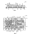
- FIGS. 7-8 show examples of assemblies 76 and 116 .
- Assembly 76 includes the baseplate 78 and substrates 6 , along with die 4 and electrical couplers 20 , of FIGS. 5-6 . Some of the electrical couplers 20 are coupled to pads 82 of the die 4 , the pads 82 being electrical contacts on a face of the die 4 .
- Assembly 116 differs from assembly 76 in that assembly 116 includes pin receiving members 118 .
- Assembly 116 is a conventional assembly that is used with conventional pins. Conventional pins do not include an elastic portion and, furthermore, with packages that use a baseplate, the pins in some cases are not coupled directly to the substrate(s) atop the baseplate for a variety of reasons.
- pin receiving members 118 may be placed atop the baseplate and contacts of the pin receiving members may be electrically coupled to contacts of elements atop the substrate 6 using electrical couplers 20 , which in implementations may be aluminum wires.
- electrical couplers 20 which in implementations may be aluminum wires.
- the housing is placed atop the assembly 116 , and when the package is installed, such as using a press-fit method with a motherboard or printed circuit board (PCB), or the like
- the forces of press-fit installation will push down on the conventional pins but will not push down directly on the substrate 6 because the pins are positioned over the pin receiving members 118 instead of over the substrate.
- the conventional pins will thus press down instead on the baseplate 78 . This may reduce the likelihood of damage to the substrate 6 during press-fit installation of the package with a motherboard, PCB or the like.
- the pin receiving members 118 may not be needed since during press-fit installation of the package 62 the pins 86 , if they are pressed down, the members 118 do not impart undue pressure onto the substrate 6 because of the reversibly elastically deformable lower portion (elastic portion) (lower portion) 92 which includes spring 94 .
- package 62 may be formed with the pins 86 landing directly on the substrate 6 instead of on pin receiving members 118 of the baseplate 78 . Accordingly, pin receiving members 118 may be excluded, and thus assembly 76 may be used instead of assembly 116 .
- the package may be reduced in size because of this, with the baseplate 78 and the housing 64 having a smaller area and/or footprint, due to the lack of need to use pin receiving members 118 .
- Package implementations in which pin receiving members 118 are excluded may also have improved operation and/or life by eliminating aluminum wirebonds.
- the same size housing 64 and baseplate 78 could be used and one or more of the pins 86 are formed with a horizontal section 112 so that the pins 86 , instead of landing on the baseplate 78 , extend inwards to land on the substrate 6 .
- a perimeter defined by a plurality of elastic couplers 84 outside the package such as shown with semiconductor package (package) 120 of FIG. 9 , may be smaller than a perimeter formed by the same plurality of elastic couplers 84 within the package.
- the housing 122 may be used with assembly 76 , but an outer perimeter defined by the elastic couplers 84 , as seen in FIG.
- packages 9 may be larger than an outer perimeter formed by a plurality of substrates 6 . Additionally some packages, such as package 120 , may have pins only along a single rectangular perimeter, while others, as packages 2 and 62 , may have pins not only along a rectangular perimeter but also within the rectangle defined by that perimeter.
- the cavity of package 120 may be partially or fully filled with an encapsulant through an opening in the housing 122 (which in FIG. 9 is rectangular) which is later covered with cover 124 .
- the pins 86 include, along with the horizontal section 112 , a first vertical section 110 and a second vertical section 114 . Furthermore, an upper portion 88 of the pin 86 includes a rigid portion 90 , and the spring 94 in implementations includes a helical coil spring 96 . The spring 94 couples the rigid portion 90 with rigid portion 98 . A lower end 100 of the pin 86 is defined as a lower end of the rigid portion 98 , if rigid portion 98 is included, or the lower end of spring 94 if rigid portion 98 is excluded, similar to pin 38 .
- the rigid portion 98 in implementations includes a flat plate 104 having a contact surface 106 on a base 102 of the flat plate 104 .
- the pin 86 has a longest length 108 that is substantially parallel, or parallel, with a direction of compression of spring 94 .
- wires of aluminum or another metal may be used to electrically couple one or more connection traces of the substrate with one or more pins of the package.
- Implementations of semiconductor packages 2 , 62 , 120 disclosed herein allow electrical interconnection between the die and pins of the package without the use of wirebonds or wire connections between the substrate and pins.
- Conventional packages use soldering to electrically and mechanically couple pins of the package with connection traces of the substrate, and thereafter a housing (such as a polymer case) is coupled to the substrate and/or a baseplate coupled to the substrate.
- the conventional housing has openings for the pins to pass through as the housing is being lowered towards the substrate and, therefore, the pins are not fixedly coupled to the housing.
- an encapsulant such as silicone potting
- the pins are nevertheless not generally fixedly coupled to the housing itself.
- the housing cannot be lifted without twisting the pin to reverse the locking procedure, and the pin is fixedly coupled to the substrate with solder, such that the housing could not be lifted relative to the substrate, without twisting the pin to the open position, without fracturing the solder connection of the pin with the substrate.
- the pin is only temporarily fixedly coupled to the housing.
- the pins are permanently fixedly coupled to the housing by being at least partially encapsulated within the housing during formation of the housing.
- the housing after the pins have been at least partially encapsulated therein, is not free to move without moving the pins as well.
- the pins could be only temporarily fixedly coupled to the housing, such as with threads, a friction fit, or the like.
- the plastic injection mold chase may be designed to arrange the pins before plastic injection.
- Each spring as disclosed herein is integrated with one of the pins in the longitudinal direction.
- pressure between the individual pins and the substrate is maintained by virtue of the plastic case being coupled with the substrate.
- the pins as described herein may be configured to be press-fit pins, such as to be press fit into hollow pin receivers of a motherboard or PCB, or they may be solder pins, configured to be soldered to connection traces or other elements of a motherboard, PCB or the like.
- the pins are press fit pins they may have a press fit portion proximate a distal end (opposite the end closest to the elastic portion or spring).
- the press fit portion may include elements such as, by non-limiting example, a compressible section that is configured to compress along a direction perpendicular with the direction of insertion of the pin into a pin receiver, which compression may comprise only elastic or may comprise elastic and plastic deformation.
- the compressible section may include an opening passing through the pin along a direction perpendicular with a longest length of the pin, though in implementations the compressible section may include other elements and/or the press fit portion may exclude an opening.
- a wide variety of other type of press-fit sections and designs may be utilized and selected by those of ordinary skill in the art using the principles disclosed herein.
- the flat plate 56 , 104 shown in the drawings has a width, substantially parallel with a longest length 60 , 108 of the pin 38 , 86 , that is greater than a height of the flat plate 56 , 104 —the height being substantially parallel with a longest length 60 , 108 of the pin 38 , 86 —in other implementations the flat plate 56 , 104 could have a height greater than its width.
- pins 38 , 86 remove the potential for such damage due to the lack of a solder connection between the pin and substrate and due to the elastic portions 44 , 92 .
- soldering process there is no soldering process to couple the pins to the substrate, and there is no wirebond connection between the substrate and the pins.
- the lack of a solder connection between the pins and the substrate may eliminate a second solder reflow process for the assembly of the package, as a first solder reflow may have occurred when coupling the die to the substrate. This can reduce other problems, such as movement or float of the die during the second solder reflow.
- the pins 38 , 86 may increase a contact area, and otherwise improve electrical contact, between the pin and the substrate as compared with conventional pins.
- the housings disclosed herein may be laser marked, or the like, at any point in the assembly process.
Abstract
Description
Claims (13)
Priority Applications (4)
| Application Number | Priority Date | Filing Date | Title |
|---|---|---|---|
| US15/230,076 US9691732B2 (en) | 2015-02-19 | 2016-08-05 | Semiconductor package with elastic coupler and related methods |
| US15/630,112 US10319652B2 (en) | 2015-02-19 | 2017-06-22 | Semiconductor package with elastic coupler and related methods |
| US16/396,904 US10607903B2 (en) | 2015-02-19 | 2019-04-29 | Semiconductor package with elastic coupler and related methods |
| US16/799,026 US11569140B2 (en) | 2015-02-19 | 2020-02-24 | Semiconductor package with elastic coupler and related methods |
Applications Claiming Priority (2)
| Application Number | Priority Date | Filing Date | Title |
|---|---|---|---|
| US14/626,758 US9431311B1 (en) | 2015-02-19 | 2015-02-19 | Semiconductor package with elastic coupler and related methods |
| US15/230,076 US9691732B2 (en) | 2015-02-19 | 2016-08-05 | Semiconductor package with elastic coupler and related methods |
Related Parent Applications (1)
| Application Number | Title | Priority Date | Filing Date |
|---|---|---|---|
| US14/626,758 Division US9431311B1 (en) | 2015-02-19 | 2015-02-19 | Semiconductor package with elastic coupler and related methods |
Related Child Applications (1)
| Application Number | Title | Priority Date | Filing Date |
|---|---|---|---|
| US15/630,112 Continuation US10319652B2 (en) | 2015-02-19 | 2017-06-22 | Semiconductor package with elastic coupler and related methods |
Publications (2)
| Publication Number | Publication Date |
|---|---|
| US20160343683A1 US20160343683A1 (en) | 2016-11-24 |
| US9691732B2 true US9691732B2 (en) | 2017-06-27 |
Family
ID=56690008
Family Applications (5)
| Application Number | Title | Priority Date | Filing Date |
|---|---|---|---|
| US14/626,758 Active US9431311B1 (en) | 2015-02-19 | 2015-02-19 | Semiconductor package with elastic coupler and related methods |
| US15/230,076 Active US9691732B2 (en) | 2015-02-19 | 2016-08-05 | Semiconductor package with elastic coupler and related methods |
| US15/630,112 Active 2035-07-29 US10319652B2 (en) | 2015-02-19 | 2017-06-22 | Semiconductor package with elastic coupler and related methods |
| US16/396,904 Active US10607903B2 (en) | 2015-02-19 | 2019-04-29 | Semiconductor package with elastic coupler and related methods |
| US16/799,026 Active 2035-02-21 US11569140B2 (en) | 2015-02-19 | 2020-02-24 | Semiconductor package with elastic coupler and related methods |
Family Applications Before (1)
| Application Number | Title | Priority Date | Filing Date |
|---|---|---|---|
| US14/626,758 Active US9431311B1 (en) | 2015-02-19 | 2015-02-19 | Semiconductor package with elastic coupler and related methods |
Family Applications After (3)
| Application Number | Title | Priority Date | Filing Date |
|---|---|---|---|
| US15/630,112 Active 2035-07-29 US10319652B2 (en) | 2015-02-19 | 2017-06-22 | Semiconductor package with elastic coupler and related methods |
| US16/396,904 Active US10607903B2 (en) | 2015-02-19 | 2019-04-29 | Semiconductor package with elastic coupler and related methods |
| US16/799,026 Active 2035-02-21 US11569140B2 (en) | 2015-02-19 | 2020-02-24 | Semiconductor package with elastic coupler and related methods |
Country Status (1)
| Country | Link |
|---|---|
| US (5) | US9431311B1 (en) |
Cited By (2)
| Publication number | Priority date | Publication date | Assignee | Title |
|---|---|---|---|---|
| WO2019053256A1 (en) | 2017-09-15 | 2019-03-21 | Finar Module Sagl | Packaging method and joint technology for an electronic device |
| US10319652B2 (en) * | 2015-02-19 | 2019-06-11 | Semiconductor Components Industries, Llc | Semiconductor package with elastic coupler and related methods |
Families Citing this family (19)
| Publication number | Priority date | Publication date | Assignee | Title |
|---|---|---|---|---|
| SG10201504274SA (en) * | 2015-05-29 | 2016-12-29 | Delta Electronics Int’L Singapore Pte Ltd | Package assembly |
| US10825748B2 (en) * | 2015-12-15 | 2020-11-03 | Semiconductor Components Industries, Llc | Semiconductor package system and related methods |
| CN107808850B (en) * | 2016-09-08 | 2020-05-08 | 株洲中车时代电气股份有限公司 | Packaging shell for power module and method for packaging power module |
| JP2018074088A (en) * | 2016-11-02 | 2018-05-10 | 富士電機株式会社 | Semiconductor device |
| US10276472B2 (en) * | 2017-04-01 | 2019-04-30 | Ixys, Llc | Heat transfer plate having small cavities for taking up a thermal transfer material |
| JP7006024B2 (en) * | 2017-08-30 | 2022-01-24 | 富士電機株式会社 | Semiconductor devices and their manufacturing methods |
| FR3076175B1 (en) * | 2017-12-22 | 2020-01-10 | Valeo Siemens Eautomotive France Sas | REMOTE WALL ELECTRICAL EQUIPMENT |
| US10566713B2 (en) | 2018-01-09 | 2020-02-18 | Semiconductor Components Industries, Llc | Press-fit power module and related methods |
| CN108809056B (en) * | 2018-06-15 | 2019-11-19 | 西安微电子技术研究所 | A kind of three-dimensionally integrated intelligent power module and its manufacturing method |
| DE102018116429B4 (en) * | 2018-07-06 | 2020-03-05 | Semikron Elektronik Gmbh & Co. Kg | Power semiconductor device with a power semiconductor component and a housing |
| CN109326566B (en) * | 2018-09-18 | 2020-08-07 | 徐州市沂芯微电子有限公司 | Semiconductor chip packaging structure and packaging method thereof |
| DE102019111145A1 (en) * | 2019-04-30 | 2020-11-05 | Semikron Elektronik Gmbh & Co. Kg | Power semiconductor module and method for arranging this power semiconductor module on a motor |
| US11710687B2 (en) * | 2019-05-22 | 2023-07-25 | Semiconductor Components Industries, Llc | Semiconductor package with guide pin |
| CN110197824A (en) * | 2019-06-20 | 2019-09-03 | 深圳市汇川技术股份有限公司 | Intelligent power module encapsulating structure |
| CN113078127A (en) | 2020-01-05 | 2021-07-06 | 财团法人工业技术研究院 | Power module |
| CN113380730A (en) * | 2020-02-25 | 2021-09-10 | 力特半导体(无锡)有限公司 | Semiconductor package with improved clamp |
| DE102021102924A1 (en) * | 2021-02-09 | 2022-08-11 | Avl Software And Functions Gmbh | Power module with reduced intrinsic inductance |
| EP4187595A1 (en) * | 2021-11-29 | 2023-05-31 | Infineon Technologies AG | Terminal element or bus bar, and power semiconductor module arrangement comprising a terminal element or bus bar |
| EP4258832A1 (en) * | 2022-04-04 | 2023-10-11 | STMicroelectronics S.r.l. | Power module having leadframe-less signal connectors, in particular for automotive applications, and assembling method thereof |
Citations (55)
| Publication number | Priority date | Publication date | Assignee | Title |
|---|---|---|---|---|
| US4639759A (en) | 1982-11-10 | 1987-01-27 | Brown, Boveri & Cie., Ag | Power transistor module |
| US4670771A (en) | 1981-07-11 | 1987-06-02 | Brown, Boveri & Cie Ag | Rectifier module |
| US4788626A (en) | 1986-02-15 | 1988-11-29 | Brown, Boveri & Cie Ag | Power semiconductor module |
| US5306169A (en) | 1992-11-19 | 1994-04-26 | Molex Incorporated | Electrical connector for connecting printed circuit boards |
| DE4237632A1 (en) | 1992-11-07 | 1994-05-11 | Export Contor Ausenhandelsgese | Circuit arrangement |
| US5371043A (en) | 1992-11-06 | 1994-12-06 | Motorola, Inc. | Method for forming a power circuit package |
| US5465481A (en) | 1993-10-04 | 1995-11-14 | Motorola, Inc. | Method for fabricating a semiconductor package |
| US5480727A (en) | 1994-02-03 | 1996-01-02 | Motorola, Inc. | Electronic device assembly and method for making |
| US5533257A (en) | 1994-05-24 | 1996-07-09 | Motorola, Inc. | Method for forming a heat dissipation apparatus |
| US5544412A (en) | 1994-05-24 | 1996-08-13 | Motorola, Inc. | Method for coupling a power lead to a bond pad in an electronic module |
| US5565705A (en) | 1994-05-02 | 1996-10-15 | Motorola, Inc. | Electronic module for removing heat from a semiconductor die |
| US5616886A (en) | 1995-06-05 | 1997-04-01 | Motorola | Wirebondless module package |
| US5666269A (en) | 1994-01-03 | 1997-09-09 | Motorola, Inc. | Metal matrix composite power dissipation apparatus |
| DE19630173A1 (en) | 1996-07-26 | 1998-01-29 | Semikron Elektronik Gmbh | Semiconductor power module for current rectifier |
| US5786230A (en) | 1995-05-01 | 1998-07-28 | Motorola, Inc. | Method of fabricating multi-chip packages |
| US5825089A (en) | 1991-05-01 | 1998-10-20 | Spectrian, Inc. | Low thermal resistance spring biased RF semiconductor package mounting structure |
| US5898128A (en) | 1996-09-11 | 1999-04-27 | Motorola, Inc. | Electronic component |
| US5915463A (en) | 1996-03-23 | 1999-06-29 | Motorola, Inc. | Heat dissipation apparatus and method |
| US6154369A (en) | 1998-03-23 | 2000-11-28 | Motorola, Inc. | Electronic assembly for removing heat from a semiconductor device |
| US6155856A (en) | 1998-11-24 | 2000-12-05 | Sumitomo Electric Industries, Ltd. | Electronic control unit with electrical connector |
| US6511336B1 (en) | 2000-05-25 | 2003-01-28 | Illinois Tool Works Inc. | Solderless flex termination for motor tab |
| US20040067698A1 (en) | 2002-10-02 | 2004-04-08 | Ipson Lee | Electrically connecting terminal structure |
| US6787900B2 (en) | 1999-10-27 | 2004-09-07 | Mitsubishi Denki Kabushiki Kaisha | Semiconductor module and insulating substrate thereof |
| US6930879B2 (en) | 2002-05-15 | 2005-08-16 | Tyco Electronics Amp Gmbh | Electronic module |
| US6930385B2 (en) | 2002-12-20 | 2005-08-16 | Ut-Battelle, Llc | Cascaded die mountings with spring-loaded contact-bond options |
| US6958534B2 (en) | 2003-04-10 | 2005-10-25 | Semikron Elektronik Gmbh | Power semiconductor module |
| US6967849B1 (en) | 1999-12-30 | 2005-11-22 | Lg Electronics Inc. | One system module for electric/electronic appliance |
| US6997727B1 (en) | 2003-03-14 | 2006-02-14 | Zierick Manufacturing Corp | Compliant surface mount electrical contacts for circuit boards and method of making and using same |
| US7034395B2 (en) | 2001-10-10 | 2006-04-25 | Eupec Europaische Gesellschaft Fur Leistungshalbleiter Gmbh | Power semiconductor module with cooling element and pressing apparatus |
| US7042074B2 (en) | 2003-11-29 | 2006-05-09 | Semikron Elektronik Gmbh & Co., Kg | Power semiconductor module and method for producing it |
| US7187074B2 (en) | 2004-06-08 | 2007-03-06 | Fuji Electric Device Technology Co., Ltd. | Semiconductor and electronic device with spring terminal |
| US7232710B2 (en) | 2003-12-17 | 2007-06-19 | Ut-Battelle, Llc | Method of making cascaded die mountings with springs-loaded contact-bond options |
| US7264481B2 (en) | 2003-08-22 | 2007-09-04 | Abb Schweiz Ag | Pressure contract spring for contact arrangement in power semiconductor module |
| EP1933379A2 (en) | 2006-12-13 | 2008-06-18 | SEMIKRON Elektronik GmbH & Co. KG | Power semiconductor module with contact springs |
| US20090197439A1 (en) | 2008-02-02 | 2009-08-06 | Vincotech Holdings S.A.R.L. | Electrical press-in contact |
| US7589418B2 (en) | 2006-02-13 | 2009-09-15 | Semikron Elektronik Gmbh & Co. Kg | Pressure contact power semiconductor module |
| US7592698B2 (en) | 2006-02-13 | 2009-09-22 | Semikron Elektronik Gmbh & Co. Kg | Power semiconductor modules having a cooling component and method for producing them |
| US7626256B2 (en) | 2006-03-22 | 2009-12-01 | Semikron Elektronik Gmbh & Co. Kg | Compact power semiconductor module having a connecting device |
| US7683472B2 (en) | 2006-02-13 | 2010-03-23 | Semikron Electronik Gmbh & Co. Kg | Power semiconductor modules and method for producing them |
| US7701054B2 (en) | 2007-02-12 | 2010-04-20 | Infineon Technologies Ag | Power semiconductor module and method for its manufacture |
| US7741711B2 (en) | 2007-07-26 | 2010-06-22 | Semikron Elektronik Gmbh & Co. Kg | Power semiconductor module with a connected substrate carrier and production method therefor |
| US7919854B2 (en) | 2008-08-15 | 2011-04-05 | Infineon Technologies Ag | Semiconductor module with two cooling surfaces and method |
| US7982290B2 (en) | 2006-01-12 | 2011-07-19 | Palo Alto Research Center, Inc. | Contact spring application to semiconductor devices |
| US20110260315A1 (en) | 2010-04-21 | 2011-10-27 | Mitsubishi Electric Corporation | Power block and power semiconductor module using same |
| US20110278706A1 (en) | 2010-05-11 | 2011-11-17 | iQXPRZ Power Inc. | Power Electronic Device Package |
| US8087943B2 (en) | 2008-01-23 | 2012-01-03 | Infineon Technologies Ag | Power semiconductor module including a contact element |
| US8130499B2 (en) | 2007-11-30 | 2012-03-06 | Panasonic Corporation | Heat dissipating structure base board, module using heat dissipating structure base board, and method for manufacturing heat dissipating structure base board |
| US8182273B2 (en) | 2008-11-19 | 2012-05-22 | Semikron Elektronik Gmbh & Co. Kg | Power semiconductor module with prestressed auxiliary contact spring |
| US20130020694A1 (en) | 2011-07-19 | 2013-01-24 | Zhenxian Liang | Power module packaging with double sided planar interconnection and heat exchangers |
| US8534641B2 (en) | 2007-12-04 | 2013-09-17 | Robert Bosch Gmbh | Connecting element and associated fluid assembly |
| US20140003013A1 (en) | 2012-06-29 | 2014-01-02 | Samsung Electro-Mechanics Co., Ltd. | Power module package and method for manufacturing the same |
| US20140001619A1 (en) | 2012-06-29 | 2014-01-02 | Samsung Electro-Mechanics Co., Ltd. | Power module package and method for manufacturing the same |
| US8690586B2 (en) | 2011-05-17 | 2014-04-08 | Interplex Industries, Inc. | Inter-board connection system with compliant flexible pin deformation prevention |
| US20140199861A1 (en) | 2013-01-14 | 2014-07-17 | Vishay General Semiconductor Llc | Electrical press-fit pin for a semiconductor module |
| US20140206122A1 (en) | 2013-01-23 | 2014-07-24 | Microchip Technology Incorporated | Open Cavity Plastic Package |
Family Cites Families (1)
| Publication number | Priority date | Publication date | Assignee | Title |
|---|---|---|---|---|
| US9431311B1 (en) * | 2015-02-19 | 2016-08-30 | Semiconductor Components Industries, Llc | Semiconductor package with elastic coupler and related methods |
-
2015
- 2015-02-19 US US14/626,758 patent/US9431311B1/en active Active
-
2016
- 2016-08-05 US US15/230,076 patent/US9691732B2/en active Active
-
2017
- 2017-06-22 US US15/630,112 patent/US10319652B2/en active Active
-
2019
- 2019-04-29 US US16/396,904 patent/US10607903B2/en active Active
-
2020
- 2020-02-24 US US16/799,026 patent/US11569140B2/en active Active
Patent Citations (57)
| Publication number | Priority date | Publication date | Assignee | Title |
|---|---|---|---|---|
| US4670771A (en) | 1981-07-11 | 1987-06-02 | Brown, Boveri & Cie Ag | Rectifier module |
| US4639759A (en) | 1982-11-10 | 1987-01-27 | Brown, Boveri & Cie., Ag | Power transistor module |
| US4788626A (en) | 1986-02-15 | 1988-11-29 | Brown, Boveri & Cie Ag | Power semiconductor module |
| US5825089A (en) | 1991-05-01 | 1998-10-20 | Spectrian, Inc. | Low thermal resistance spring biased RF semiconductor package mounting structure |
| US5508559A (en) | 1992-11-06 | 1996-04-16 | Motorola, Inc. | Power circuit package |
| US5371043A (en) | 1992-11-06 | 1994-12-06 | Motorola, Inc. | Method for forming a power circuit package |
| DE4237632A1 (en) | 1992-11-07 | 1994-05-11 | Export Contor Ausenhandelsgese | Circuit arrangement |
| US5306169A (en) | 1992-11-19 | 1994-04-26 | Molex Incorporated | Electrical connector for connecting printed circuit boards |
| US5465481A (en) | 1993-10-04 | 1995-11-14 | Motorola, Inc. | Method for fabricating a semiconductor package |
| US5666269A (en) | 1994-01-03 | 1997-09-09 | Motorola, Inc. | Metal matrix composite power dissipation apparatus |
| US5480727A (en) | 1994-02-03 | 1996-01-02 | Motorola, Inc. | Electronic device assembly and method for making |
| US5565705A (en) | 1994-05-02 | 1996-10-15 | Motorola, Inc. | Electronic module for removing heat from a semiconductor die |
| US5533257A (en) | 1994-05-24 | 1996-07-09 | Motorola, Inc. | Method for forming a heat dissipation apparatus |
| US5544412A (en) | 1994-05-24 | 1996-08-13 | Motorola, Inc. | Method for coupling a power lead to a bond pad in an electronic module |
| US5786230A (en) | 1995-05-01 | 1998-07-28 | Motorola, Inc. | Method of fabricating multi-chip packages |
| US5616886A (en) | 1995-06-05 | 1997-04-01 | Motorola | Wirebondless module package |
| US5915463A (en) | 1996-03-23 | 1999-06-29 | Motorola, Inc. | Heat dissipation apparatus and method |
| DE19630173A1 (en) | 1996-07-26 | 1998-01-29 | Semikron Elektronik Gmbh | Semiconductor power module for current rectifier |
| US5898128A (en) | 1996-09-11 | 1999-04-27 | Motorola, Inc. | Electronic component |
| US6154369A (en) | 1998-03-23 | 2000-11-28 | Motorola, Inc. | Electronic assembly for removing heat from a semiconductor device |
| US6155856A (en) | 1998-11-24 | 2000-12-05 | Sumitomo Electric Industries, Ltd. | Electronic control unit with electrical connector |
| US6787900B2 (en) | 1999-10-27 | 2004-09-07 | Mitsubishi Denki Kabushiki Kaisha | Semiconductor module and insulating substrate thereof |
| US6967849B1 (en) | 1999-12-30 | 2005-11-22 | Lg Electronics Inc. | One system module for electric/electronic appliance |
| US6511336B1 (en) | 2000-05-25 | 2003-01-28 | Illinois Tool Works Inc. | Solderless flex termination for motor tab |
| US7034395B2 (en) | 2001-10-10 | 2006-04-25 | Eupec Europaische Gesellschaft Fur Leistungshalbleiter Gmbh | Power semiconductor module with cooling element and pressing apparatus |
| US6930879B2 (en) | 2002-05-15 | 2005-08-16 | Tyco Electronics Amp Gmbh | Electronic module |
| US20040067698A1 (en) | 2002-10-02 | 2004-04-08 | Ipson Lee | Electrically connecting terminal structure |
| US6930385B2 (en) | 2002-12-20 | 2005-08-16 | Ut-Battelle, Llc | Cascaded die mountings with spring-loaded contact-bond options |
| US6997727B1 (en) | 2003-03-14 | 2006-02-14 | Zierick Manufacturing Corp | Compliant surface mount electrical contacts for circuit boards and method of making and using same |
| US6958534B2 (en) | 2003-04-10 | 2005-10-25 | Semikron Elektronik Gmbh | Power semiconductor module |
| US7264481B2 (en) | 2003-08-22 | 2007-09-04 | Abb Schweiz Ag | Pressure contract spring for contact arrangement in power semiconductor module |
| US7042074B2 (en) | 2003-11-29 | 2006-05-09 | Semikron Elektronik Gmbh & Co., Kg | Power semiconductor module and method for producing it |
| US7232710B2 (en) | 2003-12-17 | 2007-06-19 | Ut-Battelle, Llc | Method of making cascaded die mountings with springs-loaded contact-bond options |
| US7187074B2 (en) | 2004-06-08 | 2007-03-06 | Fuji Electric Device Technology Co., Ltd. | Semiconductor and electronic device with spring terminal |
| US7982290B2 (en) | 2006-01-12 | 2011-07-19 | Palo Alto Research Center, Inc. | Contact spring application to semiconductor devices |
| US7589418B2 (en) | 2006-02-13 | 2009-09-15 | Semikron Elektronik Gmbh & Co. Kg | Pressure contact power semiconductor module |
| US7592698B2 (en) | 2006-02-13 | 2009-09-22 | Semikron Elektronik Gmbh & Co. Kg | Power semiconductor modules having a cooling component and method for producing them |
| US7683472B2 (en) | 2006-02-13 | 2010-03-23 | Semikron Electronik Gmbh & Co. Kg | Power semiconductor modules and method for producing them |
| US7626256B2 (en) | 2006-03-22 | 2009-12-01 | Semikron Elektronik Gmbh & Co. Kg | Compact power semiconductor module having a connecting device |
| EP1933379A2 (en) | 2006-12-13 | 2008-06-18 | SEMIKRON Elektronik GmbH & Co. KG | Power semiconductor module with contact springs |
| US7701054B2 (en) | 2007-02-12 | 2010-04-20 | Infineon Technologies Ag | Power semiconductor module and method for its manufacture |
| US7741711B2 (en) | 2007-07-26 | 2010-06-22 | Semikron Elektronik Gmbh & Co. Kg | Power semiconductor module with a connected substrate carrier and production method therefor |
| US8130499B2 (en) | 2007-11-30 | 2012-03-06 | Panasonic Corporation | Heat dissipating structure base board, module using heat dissipating structure base board, and method for manufacturing heat dissipating structure base board |
| US8534641B2 (en) | 2007-12-04 | 2013-09-17 | Robert Bosch Gmbh | Connecting element and associated fluid assembly |
| US8087943B2 (en) | 2008-01-23 | 2012-01-03 | Infineon Technologies Ag | Power semiconductor module including a contact element |
| US20090197439A1 (en) | 2008-02-02 | 2009-08-06 | Vincotech Holdings S.A.R.L. | Electrical press-in contact |
| US7867016B2 (en) | 2008-02-02 | 2011-01-11 | Vincotech Holdings S.A.R.L. | Electrical press-in contact |
| US7919854B2 (en) | 2008-08-15 | 2011-04-05 | Infineon Technologies Ag | Semiconductor module with two cooling surfaces and method |
| US8182273B2 (en) | 2008-11-19 | 2012-05-22 | Semikron Elektronik Gmbh & Co. Kg | Power semiconductor module with prestressed auxiliary contact spring |
| US20110260315A1 (en) | 2010-04-21 | 2011-10-27 | Mitsubishi Electric Corporation | Power block and power semiconductor module using same |
| US20110278706A1 (en) | 2010-05-11 | 2011-11-17 | iQXPRZ Power Inc. | Power Electronic Device Package |
| US8690586B2 (en) | 2011-05-17 | 2014-04-08 | Interplex Industries, Inc. | Inter-board connection system with compliant flexible pin deformation prevention |
| US20130020694A1 (en) | 2011-07-19 | 2013-01-24 | Zhenxian Liang | Power module packaging with double sided planar interconnection and heat exchangers |
| US20140001619A1 (en) | 2012-06-29 | 2014-01-02 | Samsung Electro-Mechanics Co., Ltd. | Power module package and method for manufacturing the same |
| US20140003013A1 (en) | 2012-06-29 | 2014-01-02 | Samsung Electro-Mechanics Co., Ltd. | Power module package and method for manufacturing the same |
| US20140199861A1 (en) | 2013-01-14 | 2014-07-17 | Vishay General Semiconductor Llc | Electrical press-fit pin for a semiconductor module |
| US20140206122A1 (en) | 2013-01-23 | 2014-07-24 | Microchip Technology Incorporated | Open Cavity Plastic Package |
Non-Patent Citations (26)
| Title |
|---|
| "Ball grid array," published online by Wikipedia at least as early as Dec. 8, 2014, available online at http://en.wikipedia.org/wiki/Ball-grid-array, last visited Dec. 8, 2014. |
| "Clamshell Spring Pin BGA Socket for ASE's 36 Balls FCCSP," published online by Ironwood Electronics at least as early as Dec. 8, 2014, available online at http://www.ironwoodelectronics.com/press/clamshell-socket-FCCSP.cfm, last visited Dec. 8, 2014. |
| "Fuji IGBT Module Mounting instruction," published online at least as early as Dec. 4, 2014 by Fuji Electric Co., Ltd., available online at http://www.fujielectric.com/products/semiconductor/technical/mounting/box/doc/MT-IGBT/MT-IGBT-E-a.pdf, last visited Dec. 4, 2014. |
| "Power Modules 2012/2013," catalog published online by Vincotech GmbH of Unterhaching, Germany at least as early as Dec. 31, 2012, available online at http://www.vincotech.com/fileadmin/downloads/power/Vincotech-Power-Modules-Catalog-2012-13.pdf, last visited Jan. 21, 2015. |
| "Power Modules 2013/14 Speed and Flexibility," catalog published online by Vincotech GmbH of Unterhaching, Germany at least as early as Dec. 31, 2013, available online at http://www.vincotech.com/fileadmin/downloads/power/Vincotech-Power-Modules-Catalog-2013-14.pdf, last visited Jan. 21, 2015. |
| "SKiiP Technology," published online at least as early as Dec. 5, 2014 by Semikron International, GmbH, available online at http://www.semikron.com/innovation-technology/construction-and-connection-technology/skiip-technology.html, last visited Dec. 5, 2014. |
| "Spring Pin Sockets," published online by Ironwood Electronics at least as early as Dec. 8, 2014, available online at http://www.ironwoodelectronics.com/products/sockets/spring-pin-sockets.cfm, last visited Dec. 8, 2014. |
| "SPRiNG Technology,"published online at least as early as Dec. 5, 2014 by Semikron International GmbH, available online at http://www.semikron.com/innovation-technology/construction-and-connection-technology/spring-technology.html, last visited Dec. 5, 2014. |
| "Ball grid array," published online by Wikipedia at least as early as Dec. 8, 2014, available online at http://en.wikipedia.org/wiki/Ball—grid—array, last visited Dec. 8, 2014. |
| "Clamshell Spring Pin BGA Socket for ASE's 36 Balls FCCSP," published online by Ironwood Electronics at least as early as Dec. 8, 2014, available online at http://www.ironwoodelectronics.com/press/clamshell—socket—FCCSP.cfm, last visited Dec. 8, 2014. |
| "Fuji IGBT Module Mounting instruction," published online at least as early as Dec. 4, 2014 by Fuji Electric Co., Ltd., available online at http://www.fujielectric.com/products/semiconductor/technical/mounting/box/doc/MT—IGBT/MT—IGBT—E—a.pdf, last visited Dec. 4, 2014. |
| "Power Modules 2012/2013," catalog published online by Vincotech GmbH of Unterhaching, Germany at least as early as Dec. 31, 2012, available online at http://www.vincotech.com/fileadmin/downloads/power/Vincotech-Power—Modules-Catalog-2012-13.pdf, last visited Jan. 21, 2015. |
| "Power Modules 2013/14 Speed and Flexibility," catalog published online by Vincotech GmbH of Unterhaching, Germany at least as early as Dec. 31, 2013, available online at http://www.vincotech.com/fileadmin/downloads/power/Vincotech-Power—Modules-Catalog-2013-14.pdf, last visited Jan. 21, 2015. |
| "Spring Pin Sockets," published online by Ironwood Electronics at least as early as Dec. 8, 2014, available online at http://www.ironwoodelectronics.com/products/sockets/spring—pin—sockets.cfm, last visited Dec. 8, 2014. |
| Dr. James A. Forster, "Tutorial: Burn-in Sockets for Chip-Scale Packages," published online by Chip Scale Review at least as early as Dec. 8, 2014, available online at http://www.chipscalereview.com/issues/ES/issues10401/tutorial-01.html, last visited Dec. 8, 2014. |
| Dr. James A. Forster, "Tutorial: Burn-in Sockets for Chip-Scale Packages," published online by Chip Scale Review at least as early as Dec. 8, 2014, available online at http://www.chipscalereview.com/issues/ES/issues10401/tutorial—01.html, last visited Dec. 8, 2014. |
| Eugene M. Chow, Christopher Chua, Thomas Hantschel, Koenrad Van Schuylenbergh, and David K. Fork, "Pressure Contact Micro-Springs in Small Pitch Flip-Chip Packages," IEEE Transactions on Components and Packaging Technologies, vol. 29, p. 796-803, published Dec. 2006. |
| Images of pin sold and used in the U.S., at least as early as Dec. 31, 2013, by Vincotech GmbH of Unterhaching, Germany. |
| Lunya Ma, Qi Zhu, S.K. Sitaraman, Chris Chua, D.K. Fork, Abstract of "Compliant cantilevered spring interconnects for flip-chip packaging," published online at least as early as Dec. 8, 2014, available online at http://ieeexplore.ieee.org/xpl/login.jsp?tp=&arnumber=927863&url=http%3A%2F%2Fieeexplore.ieee.org%2Fxpls%2Fabs-all.jsp%3Farnumber%3D927863, last visited Dec. 8, 2014. |
| Lunya Ma, Qi Zhu, S.K. Sitaraman, Chris Chua, D.K. Fork, Abstract of "Compliant cantilevered spring interconnects for flip-chip packaging," published online at least as early as Dec. 8, 2014, available online at http://ieeexplore.ieee.org/xpl/login.jsp?tp=&arnumber=927863&url=http%3A%2F%2Fieeexplore.ieee.org%2Fxpls%2Fabs—all.jsp%3Farnumber%3D927863, last visited Dec. 8, 2014. |
| Patrick Baginski, "The Design Concepts behind Vincotech Power Modules," published online at least as early as Oct. 11, 2013, available online at http://www.vincotech.com/fileadmin/user-upload/articles/Concept-of-Vincotech-Power-Modules/Concepts%20of%20Vincotech%20power%20modules-PB.pdf, last visited Jan. 20, 2015. |
| Patrick Baginski, "The Design Concepts behind Vincotech Power Modules," published online at least as early as Oct. 11, 2013, available online at http://www.vincotech.com/fileadmin/user—upload/articles/Concept-of-Vincotech-Power-Modules/Concepts%20of%20Vincotech%20power%20modules—PB.pdf, last visited Jan. 20, 2015. |
| Ralph E. Locher, "New Packages for Pressure Mounting," published online by IXYS Corporation at least as early as Dec. 8, 2014, available online at http://www.ixys.com/Documents/AppNotes/IXAN0029.pdf, last visited Dec. 8, 2014. |
| SPRiNG Technology, Solder-free connection, by SEMIKRON, available online at http://www.semikron.com/innovation-technology/construction-and-connection-technology/spring-technology.html, last visited Jan. 30, 2015. |
| Steven H. Voldman, "ESD Basics: From Semiconductor Manufacturing to Product Use," pp. 144, 190-193, published by John Wiley & Sons, Aug. 23, 2012. |
| Trench IGBT Module, SKiM 63 Electrostatic discharge sensitive device (ESDS) by SEMIKRON, Jul. 23, 2013. |
Cited By (5)
| Publication number | Priority date | Publication date | Assignee | Title |
|---|---|---|---|---|
| US10319652B2 (en) * | 2015-02-19 | 2019-06-11 | Semiconductor Components Industries, Llc | Semiconductor package with elastic coupler and related methods |
| US10607903B2 (en) | 2015-02-19 | 2020-03-31 | Semiconductor Components Industries, Llc | Semiconductor package with elastic coupler and related methods |
| US11569140B2 (en) | 2015-02-19 | 2023-01-31 | Semiconductor Components Industries, Llc | Semiconductor package with elastic coupler and related methods |
| WO2019053256A1 (en) | 2017-09-15 | 2019-03-21 | Finar Module Sagl | Packaging method and joint technology for an electronic device |
| US11495517B2 (en) | 2017-09-15 | 2022-11-08 | Finar Module Sagl | Packaging method and joint technology for an electronic device |
Also Published As
| Publication number | Publication date |
|---|---|
| US10607903B2 (en) | 2020-03-31 |
| US10319652B2 (en) | 2019-06-11 |
| US11569140B2 (en) | 2023-01-31 |
| US20170294362A1 (en) | 2017-10-12 |
| US20190252275A1 (en) | 2019-08-15 |
| US20200194322A1 (en) | 2020-06-18 |
| US9431311B1 (en) | 2016-08-30 |
| US20160343683A1 (en) | 2016-11-24 |
| US20160247735A1 (en) | 2016-08-25 |
Similar Documents
| Publication | Publication Date | Title |
|---|---|---|
| US11569140B2 (en) | Semiconductor package with elastic coupler and related methods | |
| US6521982B1 (en) | Packaging high power integrated circuit devices | |
| TWI404177B (en) | Electric power semiconductor circuit device and method for making same | |
| KR100811581B1 (en) | Semiconductor device using bumps, method for fabricating same, and method for forming bumps | |
| KR101728264B1 (en) | Power semiconductor device | |
| US8129225B2 (en) | Method of manufacturing an integrated circuit module | |
| US20090261462A1 (en) | Semiconductor package with stacked die assembly | |
| US20160240452A1 (en) | Semiconductor packages with sub-terminals and related methods | |
| EP1628344A2 (en) | Method of making an encapsulated microelectronic package having fluid carrying encapsulant channels | |
| KR20090104477A (en) | Semiconductor Device Package | |
| US10693270B2 (en) | Press-fit pin for semiconductor packages and related methods | |
| US20160225685A1 (en) | Semiconductor device and method for manufacturing same | |
| US20210265248A1 (en) | Housings for semiconductor packages and related methods | |
| US11315856B2 (en) | Leadframe with sockets for solderless pins | |
| CN104600038B (en) | Semiconductor device | |
| US20230327350A1 (en) | Transfer molded power modules and methods of manufacture | |
| US20130256920A1 (en) | Semiconductor device | |
| US7447041B2 (en) | Compression connection for vertical IC packages | |
| CN110970372A (en) | Semiconductor device assembly including spacer with embedded semiconductor die | |
| KR101569769B1 (en) | Semiconductor package with clip structure and fabricating method for the same | |
| US20110163432A1 (en) | Semiconductor device and method of manufacturing the same | |
| US20050196907A1 (en) | Underfill system for die-over-die arrangements | |
| CN107221519B (en) | System-in-package module | |
| CN215578514U (en) | Electronic device with top surface radiating packaging structure | |
| KR101502668B1 (en) | Power module package and method for manufacturing the same |
Legal Events
| Date | Code | Title | Description |
|---|---|---|---|
| AS | Assignment |
Owner name: SEMICONDUCTOR COMPONENTS INDUSTRIES, LLC, ARIZONA Free format text: ASSIGNMENT OF ASSIGNORS INTEREST;ASSIGNORS:LIN, YUSHENG;CHEW, CHEE HIONG;CARNEY, FRANCIS J.;SIGNING DATES FROM 20150211 TO 20150217;REEL/FRAME:039358/0171 |
|
| AS | Assignment |
Owner name: DEUTSCHE BANK AG NEW YORK BRANCH, NEW YORK Free format text: SECURITY INTEREST;ASSIGNOR:SEMICONDUCTOR COMPONENTS INDUSTRIES, LLC;REEL/FRAME:041187/0295 Effective date: 20161221 |
|
| STCF | Information on status: patent grant |
Free format text: PATENTED CASE |
|
| MAFP | Maintenance fee payment |
Free format text: PAYMENT OF MAINTENANCE FEE, 4TH YEAR, LARGE ENTITY (ORIGINAL EVENT CODE: M1551); ENTITY STATUS OF PATENT OWNER: LARGE ENTITY Year of fee payment: 4 |
|
| AS | Assignment |
Owner name: FAIRCHILD SEMICONDUCTOR CORPORATION, ARIZONA Free format text: RELEASE OF SECURITY INTEREST IN PATENTS RECORDED AT REEL 041187, FRAME 0295;ASSIGNOR:DEUTSCHE BANK AG NEW YORK BRANCH, AS COLLATERAL AGENT;REEL/FRAME:064151/0203 Effective date: 20230622 Owner name: SEMICONDUCTOR COMPONENTS INDUSTRIES, LLC, ARIZONA Free format text: RELEASE OF SECURITY INTEREST IN PATENTS RECORDED AT REEL 041187, FRAME 0295;ASSIGNOR:DEUTSCHE BANK AG NEW YORK BRANCH, AS COLLATERAL AGENT;REEL/FRAME:064151/0203 Effective date: 20230622 |