US9558946B2 - FinFETs and methods of forming FinFETs - Google Patents
FinFETs and methods of forming FinFETs Download PDFInfo
- Publication number
- US9558946B2 US9558946B2 US14/506,348 US201414506348A US9558946B2 US 9558946 B2 US9558946 B2 US 9558946B2 US 201414506348 A US201414506348 A US 201414506348A US 9558946 B2 US9558946 B2 US 9558946B2
- Authority
- US
- United States
- Prior art keywords
- fin
- fins
- forming
- region
- substrate
- Prior art date
- Legal status (The legal status is an assumption and is not a legal conclusion. Google has not performed a legal analysis and makes no representation as to the accuracy of the status listed.)
- Expired - Fee Related
Links
Images


Classifications
-
- H—ELECTRICITY
- H10—SEMICONDUCTOR DEVICES; ELECTRIC SOLID-STATE DEVICES NOT OTHERWISE PROVIDED FOR
- H10D—INORGANIC ELECTRIC SEMICONDUCTOR DEVICES
- H10D30/00—Field-effect transistors [FET]
- H10D30/60—Insulated-gate field-effect transistors [IGFET]
- H10D30/62—Fin field-effect transistors [FinFET]
-
- H01L21/2236—
-
- H—ELECTRICITY
- H10—SEMICONDUCTOR DEVICES; ELECTRIC SOLID-STATE DEVICES NOT OTHERWISE PROVIDED FOR
- H10P—GENERIC PROCESSES OR APPARATUS FOR THE MANUFACTURE OR TREATMENT OF DEVICES COVERED BY CLASS H10
- H10P32/00—Diffusion of dopants within, into or out of wafers, substrates or parts of devices
- H10P32/10—Diffusion of dopants within, into or out of semiconductor bodies or layers
- H10P32/12—Diffusion of dopants within, into or out of semiconductor bodies or layers between a solid phase and a gaseous phase
- H10P32/1204—Diffusion of dopants within, into or out of semiconductor bodies or layers between a solid phase and a gaseous phase from a plasma phase
-
- H01L21/02362—
-
- H01L21/02694—
-
- H01L21/2252—
-
- H01L21/31155—
-
- H01L29/66795—
-
- H01L29/785—
-
- H—ELECTRICITY
- H10—SEMICONDUCTOR DEVICES; ELECTRIC SOLID-STATE DEVICES NOT OTHERWISE PROVIDED FOR
- H10D—INORGANIC ELECTRIC SEMICONDUCTOR DEVICES
- H10D30/00—Field-effect transistors [FET]
- H10D30/01—Manufacture or treatment
- H10D30/021—Manufacture or treatment of FETs having insulated gates [IGFET]
- H10D30/024—Manufacture or treatment of FETs having insulated gates [IGFET] of fin field-effect transistors [FinFET]
- H10D30/0241—Manufacture or treatment of FETs having insulated gates [IGFET] of fin field-effect transistors [FinFET] doping of vertical sidewalls, e.g. using tilted or multi-angled implants
-
- H—ELECTRICITY
- H10—SEMICONDUCTOR DEVICES; ELECTRIC SOLID-STATE DEVICES NOT OTHERWISE PROVIDED FOR
- H10D—INORGANIC ELECTRIC SEMICONDUCTOR DEVICES
- H10D62/00—Semiconductor bodies, or regions thereof, of devices having potential barriers
- H10D62/60—Impurity distributions or concentrations
-
- H—ELECTRICITY
- H10—SEMICONDUCTOR DEVICES; ELECTRIC SOLID-STATE DEVICES NOT OTHERWISE PROVIDED FOR
- H10D—INORGANIC ELECTRIC SEMICONDUCTOR DEVICES
- H10D64/00—Electrodes of devices having potential barriers
- H10D64/01—Manufacture or treatment
- H10D64/017—Manufacture or treatment using dummy gates in processes wherein at least parts of the final gates are self-aligned to the dummy gates, i.e. replacement gate processes
-
- H—ELECTRICITY
- H10—SEMICONDUCTOR DEVICES; ELECTRIC SOLID-STATE DEVICES NOT OTHERWISE PROVIDED FOR
- H10P—GENERIC PROCESSES OR APPARATUS FOR THE MANUFACTURE OR TREATMENT OF DEVICES COVERED BY CLASS H10
- H10P14/00—Formation of materials, e.g. in the shape of layers or pillars
- H10P14/20—Formation of materials, e.g. in the shape of layers or pillars of semiconductor materials
- H10P14/38—Formation of materials, e.g. in the shape of layers or pillars of semiconductor materials characterised by treatments done after the formation of the materials
- H10P14/3822—Controlling the interface between substrate and epitaxial layer, e.g. by ion implantation followed by annealing
-
- H—ELECTRICITY
- H10—SEMICONDUCTOR DEVICES; ELECTRIC SOLID-STATE DEVICES NOT OTHERWISE PROVIDED FOR
- H10P—GENERIC PROCESSES OR APPARATUS FOR THE MANUFACTURE OR TREATMENT OF DEVICES COVERED BY CLASS H10
- H10P14/00—Formation of materials, e.g. in the shape of layers or pillars
- H10P14/60—Formation of materials, e.g. in the shape of layers or pillars of insulating materials
- H10P14/65—Formation of materials, e.g. in the shape of layers or pillars of insulating materials characterised by treatments performed before or after the formation of the materials
- H10P14/6516—Formation of materials, e.g. in the shape of layers or pillars of insulating materials characterised by treatments performed before or after the formation of the materials of treatments performed after formation of the materials
- H10P14/6548—Formation of materials, e.g. in the shape of layers or pillars of insulating materials characterised by treatments performed before or after the formation of the materials of treatments performed after formation of the materials by forming intermediate materials, e.g. capping layers or diffusion barriers
-
- H—ELECTRICITY
- H10—SEMICONDUCTOR DEVICES; ELECTRIC SOLID-STATE DEVICES NOT OTHERWISE PROVIDED FOR
- H10P—GENERIC PROCESSES OR APPARATUS FOR THE MANUFACTURE OR TREATMENT OF DEVICES COVERED BY CLASS H10
- H10P30/00—Ion implantation into wafers, substrates or parts of devices
- H10P30/40—Ion implantation into wafers, substrates or parts of devices into insulating materials
-
- H—ELECTRICITY
- H10—SEMICONDUCTOR DEVICES; ELECTRIC SOLID-STATE DEVICES NOT OTHERWISE PROVIDED FOR
- H10P—GENERIC PROCESSES OR APPARATUS FOR THE MANUFACTURE OR TREATMENT OF DEVICES COVERED BY CLASS H10
- H10P32/00—Diffusion of dopants within, into or out of wafers, substrates or parts of devices
- H10P32/10—Diffusion of dopants within, into or out of semiconductor bodies or layers
- H10P32/14—Diffusion of dopants within, into or out of semiconductor bodies or layers within a single semiconductor body or layer in a solid phase; between different semiconductor bodies or layers, both in a solid phase
- H10P32/1404—Diffusion of dopants within, into or out of semiconductor bodies or layers within a single semiconductor body or layer in a solid phase; between different semiconductor bodies or layers, both in a solid phase using predeposition followed by drive-in of impurities into the semiconductor surface, e.g. predeposition from a gaseous phase
-
- H—ELECTRICITY
- H10—SEMICONDUCTOR DEVICES; ELECTRIC SOLID-STATE DEVICES NOT OTHERWISE PROVIDED FOR
- H10P—GENERIC PROCESSES OR APPARATUS FOR THE MANUFACTURE OR TREATMENT OF DEVICES COVERED BY CLASS H10
- H10P32/00—Diffusion of dopants within, into or out of wafers, substrates or parts of devices
- H10P32/10—Diffusion of dopants within, into or out of semiconductor bodies or layers
- H10P32/17—Diffusion of dopants within, into or out of semiconductor bodies or layers characterised by the semiconductor material
- H10P32/171—Diffusion of dopants within, into or out of semiconductor bodies or layers characterised by the semiconductor material being group IV material
Definitions
- Semiconductor devices are used in a large number of electronic devices, such as computers, cell phones, and others.
- Semiconductor devices comprise integrated circuits that are formed on semiconductor wafers by depositing many types of thin films of material over the semiconductor wafers, and patterning the thin films of material to form the integrated circuits.
- Integrated circuits typically include field-effect transistors (FETs).
- planar FETs have been used in integrated circuits.
- planar FETs may generally incur problems when reduced in size.
- Some of these problems include sub-threshold swing degradation, significant drain induced barrier lowering (DIBL), fluctuation of device characteristics, and leakage.
- Fin field-effect transistors (FinFETs) have been studied to overcome some of these problems.
- FIG. 1 is an example of a Fin Field-Effect Transistor (FinFET) in a three-dimensional view.
- FinFET Fin Field-Effect Transistor
- FIGS. 2A-C , 3 A-C, 4 A-C, 5 A-C, 6 A-C, 7 A-C, 8 A-D, 9 A-C, 10 A-C, 11 A-C, 12 A-D, and 13 A- 13 C are cross-sectional views of intermediate stages in the manufacturing of FinFETs in accordance with some embodiments.
- FIGS. 14A and 14B are a process flow of a process in accordance with some embodiments.
- FIGS. 15A-C are doping profiles of structures in accordance with some embodiments.
- first and second features are formed in direct contact
- additional features may be formed between the first and second features, such that the first and second features may not be in direct contact
- present disclosure may repeat reference numerals and/or letters in the various examples. This repetition is for the purpose of simplicity and clarity and does not in itself dictate a relationship between the various embodiments and/or configurations discussed.
- spatially relative terms such as “beneath,” “below,” “lower,” “above,” “upper” and the like, may be used herein for ease of description to describe one element or feature's relationship to another element(s) or feature(s) as illustrated in the figures.
- the spatially relative terms are intended to encompass different orientations of the device in use or operation in addition to the orientation depicted in the figures.
- the apparatus may be otherwise oriented (rotated 90 degrees or at other orientations) and the spatially relative descriptors used herein may likewise be interpreted accordingly.
- Fin Field-Effect Transistors Fin Field-Effect Transistors
- Methods are discussed in a particular order, various other method embodiments may be performed in any logical order and may include fewer or more steps described herein.
- FIG. 1 illustrates an example of a FinFET 30 in a three-dimensional view.
- the FinFET 30 comprises a fin 36 on a substrate 32 .
- the substrate 32 includes isolation regions 34 , and the fin 36 protrudes above and from between neighboring isolation regions 34 .
- a gate dielectric 38 is along sidewalls and over a top surface of the fin 36 , and a gate electrode 40 is over the gate dielectric 38 .
- Source/drain regions 42 and 44 are disposed in opposite sides of the fin 36 with respect to the gate dielectric 38 and gate electrode 40 .
- FIG. 1 further illustrates reference cross-sections that are used in later figures.
- Cross-section A-A is along a longitudinal axis of the fin 36 and in a direction of, for example, a current flow between the source/drain regions 42 and 44 .
- Cross-section B-B is perpendicular to cross-section A-A and across a channel, gate dielectric 38 , and gate electrode 40 of the FinFET 30 .
- Cross-section C-C is parallel to cross-section B-B and across a source/drain region. Subsequent figures refer to these reference cross-sections for clarity.
- FIGS. 2A through 13C are cross-sectional views of intermediate stages in the manufacturing of FinFETs in accordance with an exemplary embodiment
- FIGS. 14A and 14B are a process flow of the process shown in FIGS. 2 through 13C
- Figures ending with an “A” designation are illustrated along cross-section A-A illustrated in FIG. 1
- figures ending with a “B” designation are illustrated along a similar cross-section B-B
- figures ending with a “C” designation are illustrated along a similar cross-section C-C, except for multiple FinFETs.
- FIGS. 2A, 2B, and 2C illustrate a substrate 50 , semiconductor strips 52 , isolation regions 54 , gate electrodes 60 , and mask layer 62 .
- Substrate 50 may be a semiconductor substrate, such as a bulk semiconductor, a semiconductor-on-insulator (SOI) substrate, or the like, which may be doped (e.g., with a p-type or an n-type dopant) or undoped.
- the substrate 50 may be a wafer, such as a silicon wafer.
- SOI substrate comprises a layer of a semiconductor material formed on an insulator layer.
- the insulator layer may be, for example, a buried oxide (BOX) layer, a silicon oxide layer, or the like.
- BOX buried oxide
- the insulator layer is provided on a substrate, typically a silicon or glass substrate.
- a substrate typically a silicon or glass substrate.
- Other substrates, such as a multi-layered or gradient substrate may also be used.
- the semiconductor material of the substrate 50 may include silicon; germanium; a compound semiconductor including silicon carbide, gallium arsenic, gallium phosphide, indium phosphide, indium arsenide, and/or indium antimonide; an alloy semiconductor including SiGe, GaAsP, AlInAs, AlGaAs, GaInAs, GaInP, and/or GaInAsP; or combinations thereof.
- the substrate 50 has a first region 50 A and a second region 50 B.
- the first region 50 A can be for forming n-type devices, such as NMOS transistors, such as n-type FinFETs.
- the second region 50 B can be for forming p-type devices, such as PMOS transistors, such as p-type FinFETs.
- the semiconductor strips 52 , isolation regions 54 , and fins 56 are formed over the substrate 50 .
- the isolation regions 54 extend from a top surface of the substrate 50 into the substrate 50 .
- the isolation regions 54 may be shallow trench isolation (STI) regions, and are referred to as STI regions 54 hereinafter.
- the formation of the STI regions 54 may include etching the substrate 50 to form trenches (not shown), and filling the trenches with a dielectric material to form the STI regions 54 .
- the STI regions 54 may be formed of an oxide, such as silicon oxide, a nitride, the like, or a combination thereof, and may be formed by a high density plasma chemical vapor deposition (HDP-CVD), a flowable CVD (FCVD) (e.g., a CVD-based material deposition in a remote plasma system and post curing to make it convert to another material, such as an oxide), the like, or a combination thereof.
- FCVD flowable CVD
- Other insulation materials formed by any acceptable process may be used.
- the insulation material is silicon oxide formed by a FCVD process.
- An anneal process may be performed once the insulation material is formed.
- the portion of substrate 50 between neighboring STI regions 54 is referred to as a semiconductor strips 52 throughout the description.
- the top surfaces of the semiconductor strips 52 and the top surfaces of the STI regions 54 may be substantially level with each other, such as by performing a chemical mechanical polish (CMP) after depositing the material of the STI regions 54 , although
- the STI regions 54 may then be recessed have portions of the semiconductor strips 52 extend above the top surfaces of the STI regions 54 .
- the protruding portions of the semiconductor strips 52 will be referred to as fins 56 hereinafter.
- the fins 56 have a height H 1 from top surfaces of the fins 56 to top surfaces of the STI regions, and the fins 56 and the semiconductor strips 52 have a combined height H 2 from top surfaces of the fins 56 to top surfaces of the substrate 50 (e.g. at the bottom of the STI regions 54 ).
- the height H 1 is from about 20 nm to about 40 nm
- the height H 2 is from about 40 nm to about 60 nm.
- a dielectric layer can be formed over a top surface of the substrate 50 ; trenches can be etched through the dielectric layer; homoepitaxial structures can be epitaxially grown in the trenches; and the dielectric layer can be recessed such that the homoepitaxial structures protrude from the dielectric layer to form fins.
- heteroepitaxial structures can be used for the fins.
- the fins 56 in FIGS. 2A through 2C can be recessed, and a material different from the fins 56 may be epitaxially grown in their place.
- a dielectric layer can be formed over a top surface of the substrate 50 ; trenches can be etched through the dielectric layer; heteroepitaxial structures can be epitaxially grown in the trenches using a material different from the substrate 50 ; and the dielectric layer can be recessed such that the heteroepitaxial structures protrude from the dielectric layer to form fins.
- the grown materials may be in situ doped during growth, which may obviate prior implanting of the fins although in situ and implantation doping may be used together. Still further, it may be advantageous to epitaxially grow a material in an NMOS region different from the material in a PMOS region.
- the fins 56 may comprise silicon germanium (Si x Ge 1-x , where x can be between approximately 0 and 100), silicon carbide, pure or substantially pure germanium, a III-V compound semiconductor, a II-VI compound semiconductor, or the like.
- the available materials for forming III-V compound semiconductor include, but are not limited to, InAs, AlAs, GaAs, InP, GaN, InGaAs, InAlAs, GaSb, AlSb, AlP, GaP, and the like.
- a gate structure is formed over the fins 56 and the STI regions 54 .
- the gate structure includes a gate dielectric layer 58 and a gate electrode 114 with a mask layer 62 over the gate electrode 60 .
- the gate structure crosses over a plurality of the fins 56 and the STI regions 54 .
- the gate structure has a longitudinal axis that is substantially perpendicular to the longitudinal axes of fins 56 .
- the gate structure is a dummy gate structure and will be replaced with a replacement gate structure using a “gate-last” or replacement-gate process.
- the gate structure is an active gate and is formed in a “gate-first process” and will not be replaced.
- a gate dielectric layer 58 may be formed and patterned to form the gate dielectric 58 ′ (see FIGS. 6A, 6B, and 6C ).
- the gate dielectric layer 58 may be formed over the fins 56 and the STI regions 54 by thermal oxidation, in-situ steam generation (ISSG) process, chemical vapor deposition (CVD), a spin-on-glass process, sputtering, or any other methods known and used in the art for forming a gate dielectric layer.
- the gate dielectric layer 58 may be made of one or more suitable dielectric materials such as silicon oxide, silicon nitride, low-k dielectrics such as carbon doped oxides, extremely low-k dielectrics such as porous carbon doped silicon dioxide, a polymer such as polyimide, the like, or a combination thereof.
- the gate dielectric layer includes dielectric materials having a high dielectric constant (k value), for example, greater than 3.9.
- the materials may include silicon nitrides, oxynitrides, metal oxides such as HfO 2 , HfZrO x , HfSiO x , HfTiO x , HfAlO x , the like, or combinations and multi-layers thereof.
- a gate electrode 60 is formed over the gate dielectric layer.
- the gate electrode 60 may be formed by first forming a gate electrode layer (not shown) over the fins 56 and the STI regions 54 and then patterning the gate electrode layer to form the gate electrode 60 .
- the gate electrode layer is a conductive material and may be selected from a group comprising polycrystalline-silicon (poly-Si), poly-crystalline silicon-germanium (poly-SiGe), metallic nitrides, metallic silicides, metallic oxides, and metals.
- the gate electrode layer includes a metal-containing material such as TiN, TaN, TaC, Co, Ru, Al, combinations thereof, or multi-layers thereof.
- the gate electrode layer may be deposited by CVD, physical vapor deposition (PVD), sputter deposition, or other techniques known and used in the art for depositing conductive materials.
- the top surface of the gate electrode layer may have a non-planar top surface and may be planarized by, for example, performing a CMP process after it is deposited.
- the mask layer 62 such as a photoresist, hard mask, combinations thereof, or multi-layers thereof—may be formed and patterned over the gate electrode layer. The patterned mask layer 62 may then be transferred to the material of the gate electrode layer using acceptable photolithography and etching techniques to form the gate electrode 60 .
- a seal spacer layer 64 is formed on the exposed surfaces of the gate electrodes 60 , mask layers 62 , on the gate dielectric layer 58 over the fins 56 , and on top surfaces of the STI regions 54 .
- the seal spacer layer 64 may be formed of an oxide, nitride, SiC, SiCN, the like, or a combination thereof by an oxidation process, CVD, the like, or a combination thereof.
- a mask 66 is formed over the second region 50 B of the substrate 50 while the first region 50 A is exposed.
- the mask protects the second region 50 B during subsequent processing of the first region 50 A.
- the mask 66 may be a photoresist, a hard mask, such as SiN, the like, or a combination thereof.
- the mask 66 is then patterned by an acceptable photolithography process or the like.
- a selective implant process 68 is performed on the first region 50 A of the substrate 50 .
- the selective implant process 68 changes the properties of the seal spacer layer 64 to allow a selective etch of the seal spacer layer 64 to remove portions of the seal spacer layer 64 while other portions of the seal spacer layer 64 remain.
- the selective implant process 68 includes implanting oxygen, fluorine, the like, or a combination thereof.
- the implanted region of the seal spacer layer 64 has a higher etch rate than the non-implanted region of the seal spacer layer 64 .
- the selective implant process 68 is performed at an angle substantially perpendicular to a major surface of the substrate 50 such that the horizontal surfaces (i.e., surfaces that are substantially parallel to the major surface of the substrate 50 ) of the seal spacer layer 64 are implanted during the selective implant process 68 while the vertical surfaces (i.e., surfaces that are substantially perpendicular to the major surface of the substrate 50 ) of the seal spacer layer 64 are not implanted.
- a selective etch process is performed on the seal spacer layer 64 and the gate dielectric layer 58 in the first region 50 A of the substrate 50 to form seal spacers 64 ′ and gate dielectric 58 ′ in the first region 50 A.
- the seal spacers 64 ′ are formed on sidewalls of the gate electrodes 60 and mask layers 62 in the first region 50 A.
- the process gas of the selective etch includes CF 4 , O 2 , and HBr, the like, or a combination thereof.
- a plasma doping process 70 is performed on the first region 50 A of the substrate 50 to form first doped regions 72 A in the fins 56 .
- the plasma doping process 70 implants n-type dopants (e.g. P, As, etc.) to form lightly doped drain (LDD) regions.
- n-type dopants e.g. P, As, etc.
- LDD lightly doped drain
- the plasma doping process 70 is performed in the first region 50 A of the substrate 50 utilizes from about 0.1% to about 0.9% of AsH 3 or PH 3 /He, and from about 99.1% to about 99.9% H 2 .
- the plasma doping process 70 is performed at a constant energy of between about 0.2 kiloelectron-volts (keV) and about 5 keV.
- the first doped regions 72 A have a dopant concentration of As/P in a range from about 1E20 atoms/cm 3 to about 3E21 atoms/cm 3 .
- the plasma doping process 70 can form an abrupt doping profile junction at a depth of from about 5 nm to about 10 nm from surfaces of the fin 56 with a doping profile abruptness of about 1 nm/decade.
- the mask 66 is removed such that the seal spacer layer 64 in the second region 50 B is exposed.
- the mask 66 may be removed by an appropriate ashing process, such as using an oxygen plasma.
- the mask 66 may be removed using an etch, a CMP process, the like, or a combination thereof.
- the mask 66 may be removed by a etch process utilizing CF 4 , O 2 , and HBr, the like, or a combination thereof.
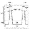
- FIG. 8D illustrates a close-up view of the fins 56 and the first poped regions 72 A from FIG. 8C .
- the first doped regions 72 A are located in top portions (tips) of the fins 56 .
- a dopant source layer 74 is formed by a plasma deposition process.
- the plasma deposition process forms a conformal layer having a substantially uniform thickness on top surfaces and sidewalls of the fins 56 in the first region 50 A and on the seal spacer layer 64 in the second region 50 B of the substrate 50 .
- the plasma deposition process utilizes from about from about 15% to about 100% of AsH 3 or PH 3 /He, and from about 85% to about 0% H 2 .
- the thickness of the dopant source layer 74 may be in a range from about 1 nm to about 5 nm, although other thicknesses are also within the scope of the present disclosure.
- the dopant source layer 74 is formed of phosphosilicate glass (PSG) and/or other materials that comprise a dopant susceptible to subsequent diffusion into the fins 56 .
- the dopant source layer 74 may be formed by sputtering, CVD, PECVD, metal organic CVD (MOCVD), furnace CVD (FCVD), atomic layer deposition (ALD), plasma-enhanced ALD (PEALD), the like, or a combination thereof.
- plasma doping process 70 was performed before the plasma deposition process, the order of these processes could be reversed in other embodiments which are within the scope of the present disclosure.
- a capping layer 76 is formed over the dopant source layer 74 in the first and second regions 50 A and 50 B of the substrate 50 .
- the capping layer 76 helps to prevent the dopant source layer 74 from evaporating during the subsequent anneal process.
- the capping layer 76 is formed of an oxide, such as Al 2 O 3 , a nitride, the like, or a combination thereof.
- the capping layer may be formed by sputtering, CVD, PECVD, MOCVD, FCVD, ALD, PEALD, the like, or a combination thereof.
- an annealing process is performed on the substrate 50 .
- FIGS. 11A, 11B, and 11C illustrate the substrate 50 after the annealing process.
- the annealing process diffuses the dopants from the dopant source layer 74 into the fins 56 and also activates the dopants in the first doped regions and the dopants from the dopant source layer 74 forming the second doped regions 72 B in the fins 56 in the first region 50 A of the substrate 50 .
- the first doped regions 72 A and the second doped regions 72 B form an LDD region for the FinFET in the first region 50 A of the substrate.
- the seal spacer layer 64 and the gate dielectric layer 58 in over the fins 56 in the second region 50 B of the substrate 50 act as blocking layers so that the dopants from the dopant source layer 74 do not diffuse into the fins 56 in the second region 50 B.
- the second doped regions 72 B extend along the top portions (tips) and sidewalls of the fins 56 and provide a substantially uniform doping profile along the sidewalls of the fins 56 .
- the second doped regions 72 B may overlap the first doped regions 72 A in the top portions (tips) of the fins 56 .
- the second doped regions 72 B have a dopant concentration of As/P in a range from about 5E19 atoms/cm 3 to about 2E20 atoms/cm 3 .
- the second doped regions 72 B can form an abrupt doping profile junction at a depth of from about 5 nm to about 10 nm from surfaces of the fin 56 .
- FIG. 11C illustrates a portion of the fins 56 between second doped regions 72 B, in some embodiments, the fins 56 are formed to have a width such that the second doped regions 72 B along the sidewalls meet to uniformly dope the entire fin 56 .
- the annealing process may include one or more annealing processes may be performed at this stage to affect the solid phase diffusion of dopant from the dopant source layer 74 into the fins 56 .
- the one or more annealing processes may entail subjecting the substrate 50 to a temperature ranging between about 100° C. and about 1200° C. for a time period ranging between about 1 second and about 10 hours.
- other annealing parameters are also within the scope of present disclosure.
- FIGS. 12A, 12B, 12C, 12D and step 224 the capping layer 76 and the dopant source layer 74 are removed from the first and second regions 50 A and 50 B of the substrate 50 .
- the capping layer 76 and the dopant source layer 74 may be removed using an etch, a CMP process, the like, or a combination thereof.
- FIG. 12D illustrates a close-up view of the fins 56 and the first doped regions 72 A and the second doped regions 72 B from FIG. 12C .
- the first doped regions 72 A are located in top portions (tips) of the fins 56 and the second doped regions 72 B are located in the sidewalls of the fins 56 .
- the fins 56 have the desired fin LDD doping profile.
- the top portions (tips) of the fins 56 have the first doped regions 72 A and are doped to a higher concentration than middle/bottom portions (sidewalls) of the fins 56 which include the second doped regions 72 B.
- This doping profile is beneficial because the top portions of the fins 56 have higher carrier flow due to a lower threshold voltage because the top portions of the fins 56 are controlled by three gates (e.g. the gate electrode 60 is on three sides of top portions) and the middle/bottom portions of the fins 56 are controlled by two gates, and thus, have a slightly higher threshold voltage and slightly lower carrier flow.
- Steps 226 - 242 perform similar processes on the second region 50 B (e.g. p-type FinFET) of the substrate 50 as steps 208 - 224 did to the first region 50 A (e.g. n-type FinFET) of the substrate 50 . Details of these steps that are similar to those described above are not repeated herein.
- step 226 a mask is formed over the first region 50 A of the substrate.
- This mask and step may be similar to the mask and step described above in step 208 and the description is not repeated herein.
- step 228 a selective implant is performed to implant dopants into the seal spacer layer 64 in the second region 50 B of the substrate 50 .
- This selective implant process and step may be similar to the selective implant process and step described above in step 210 and the description is not repeated herein.
- a selective etch is on the seal spacer layer 64 and the gate dielectric layer 58 in the second region 50 B of the substrate 50 .
- This selective etch process and step may be similar to the selective etch process and step described above in step 212 and the description is not repeated herein.
- a plasma doping process is performed on the second region 50 B of the substrate 50 to form third doped regions 82 A in the fins 56 (see FIGS. 13A, 13B, and 13C ).
- the plasma doping process implants p-type dopants (e.g. B, Ga, etc.) to form LDD regions in the fins 56 of the second region 50 B of the substrate 50 .
- the plasma doping process is performed in the second region 50 B of the substrate 50 utilizes from about 0.1% to about 0.9% of B 2 H 6 or BF 3 /H 2 , and from about 99.1% to about 99.9% He.
- the plasma doping process is performed at a constant energy of between about 2 keV and about 5 keV.
- the third doped regions 82 A have a dopant concentration of B/Ga in a range from about 1E20 atoms/cm 3 to about 3E21 atoms/cm 3 .
- the plasma doping process can form an abrupt doping profile junction at a depth of from about 5 nm to about 10 nm from surfaces of the fin 56 with a doping profile abruptness of about 1 nm/decade.
- step 234 the mask is removed from the first region 50 A of the substrate 50 .
- This mask removal process and step may be similar to the mask removal and step described above in step 216 and the description is not repeated herein.
- a dopant source layer is formed by a plasma deposition process.
- the plasma deposition process forms a conformal layer having a substantially uniform thickness on top surfaces and sidewalls of the fins 56 in the second region 50 B and on the mask layer, if present, or other protective structure in the first region 50 A of the substrate 50 .
- the plasma deposition process utilizes from about from about 15% to about 100% of B 2 H 6 or BF 3 /H 2 , and from about 85% to about 0% He.
- the thickness of the dopant source layer may be in a range from about 1 nm to about 5 nm, although other thicknesses are also within the scope of the present disclosure.
- the dopant source layer is formed of BSG, and/or other materials that comprise a dopant susceptible to subsequent diffusion into the fins 56 .
- the dopant source layer may be formed by sputtering, CVD, PECVD, MOCVD, FCVD, ALD, PEALD, the like, or a combination thereof.
- a capping layer is formed over the dopant source layer in the second region 50 B of the substrate 50 .
- the capping layer and the step may be similar to the capping layer and step described above in step 220 and the description is not repeated herein.
- step 240 an anneal process is performed on the substrate 50 .
- This annealing process diffuses the dopants from the dopant source layer into the fins 56 and also activates the dopants forming the fourth doped regions 82 B in the fins 56 in the second region 50 B of the substrate 50 .
- This annealing process and step may be similar to the annealing process and step described above in step 222 and the description is not repeated herein.
- step 242 the capping layer and dopant source layer are removed.
- This removal process and step may be similar to the removal process and step described above in step 224 and the description is not repeated herein.
- the fourth doped regions 82 B extend along the top portions (tips) and sidewalls of the fins 56 and provide a substantially uniform doping profile along the sidewalls of the fins 56 .
- the fourth doped regions 82 B may overlap the third doped regions 82 A in the top portions (tips) of the fins 56 .
- the fourth doped regions 82 B have a dopant concentration of B/Ga in a range from about 5E19 atoms/cm 3 to about 2E20 atoms/cm 3 .
- the fourth doped regions 82 B can form an abrupt doping profile junction at a depth of from about 5 nm to about 10 nm from surfaces of the fin 56 .
- FIG. 13C illustrates a portion of the fins 56 between fourth doped regions 82 B, in some embodiments, the fins 56 are formed to have a width such that the fourth doped regions 82 B along the sidewalls meet to uniformly dope the entire fin 56 .
- gate spacers may be formed on sidewalls of the gate electrodes 60 .
- the gate spacers (not shown) may be formed on opposite sides of the gate electrodes 60 .
- the gate spacers may be formed by blanket depositing a spacer layer (not shown) on the previously formed structure.
- the gate spacers may include a spacer liner (not shown) comprising SiN, SiC, SiGe, oxynitride, oxide, combinations thereof, or the like.
- the spacer layer may comprise SiN, oxynitride, SiC, SiON, oxide, combinations thereof, or the like and may be formed by methods utilized to form such a layer, such as CVD, plasma enhanced CVD, sputter, and other methods known in the art.
- the gate spacers are then patterned, for example, by anisotropically etching to remove the spacer layer from the horizontal surfaces of the structure.
- source/drain regions may be formed in the fins 56 .
- the source/drain regions (not shown in FIGS. 13A, 13B, and 13C , see source/drain regions 42 and 44 in FIG. 1 ) may be formed in the fins 56 .
- the source/drain regions may be doped by with the appropriate dopants to complement the dopants in the fins 56 .
- the source/drain regions may be formed by forming recesses in the fins 56 and epitaxially growing material in the recesses.
- the source/drain regions may be doped either through an implantation method as discussed above, or else by in-situ doping as the material is grown.
- the source/drain regions may comprise and a heavily doped region in addition to the LDD regions discussed above.
- the source/drain regions may then be heavily doped. This forms LDD regions and heavily doped regions.
- the LDD regions are primarily underneath the gate spacers while the heavily doped regions are outside of the gate spacers along the fins 56 .
- the fins 56 include an anti-punch through region (not shown). This anti-punch through region prevents the short channel effect of electrons or holes punching through the channel from the source to the drain.
- the anti-punch through region may be doped the same as the fin 56 but with a higher dopant concentration.
- an etch stop layer (ESL) and an inter-layer dielectric (ILD) may be formed over and adjoining the gate electrodes 60 and fins 56 .
- the ESL and the ILD may be formed over the gate spacers, the gate electrodes 60 , the source/drain regions, the fins 56 , and the STI regions 54 .
- the ESL may be conformally deposited over components on the substrate 50 .
- the ESL is formed of SiN, SiCN, SiON, the like, or a combination thereof and is formed by ALD, molecular layer deposition (MLD), a furnace process, CVD, PECVD, the like, or a combination thereof.
- the ILD may be formed over the ESL.
- the ILD may be conformally deposited over the ESL.
- the ILD may comprise SiO 2 , SiON, the like, or a combination thereof.
- the ILD may be formed by CVD, ALD, PECVD, subatmospheric CVD (SACVD), flowable CVD, a high density plasma (HDP), a spin-on-dielectric process, the like, or a combination thereof.
- the ILD may be planarized by using a CMP process to remove portions of the ILD.
- CMP process may be planarized by using other planarization techniques, such as etching.
- the dummy gate and gate dielectric may be removed.
- the gate electrode 60 and the gate dielectric 58 ′ are removed.
- an active gate and gate dielectric is formed in the place of the removed gate electrode and gate dielectric.
- contacts and inter-metal dielectrics (IMD) and their corresponding metallizations may be formed through the ESL and ILD to the fins 56 and the gate electrodes 60 .
- the contacts may be formed to the gate electrodes 60 and the source/drain regions.
- FIGS. 15A, 15B, and 15C are doping profiles of structures in accordance with some embodiments.
- FIG. 15A illustrates the doping profile of the fins 56 after the plasma doping process in steps 214 and 232 but without the plasma deposition process and annealing process.
- a semiconductor structure 300 is shown with an upper region 302 and a lower region 304 .
- the upper region 302 has a high dopant concentration and the lower region 304 has no doping concentration or almost zero doping concentration.
- the upper region 302 has a dopant concentration of B, Ga, As, P, the like, or a combination thereof in a range from about 1E20 atoms/cm 3 to about 3E21 atoms/cm 3 and the lower region is non-doped.
- the plasma doping process forms an abrupt junction (at the interface between the upper region 302 and the lower region 304 ) in the doping profile.
- FIG. 15B illustrates the doping profile of the fins 56 after the plasma deposition process and annealing process 218 - 222 and 236 - 240 but without the plasma doping process.
- the semiconductor structure 300 is shown with single region 306 .
- the region 306 has a uniform doping profile, but typically a lower dopant concentration than a region doped by a plasma doping process.
- the region 306 has a dopant concentration of B, Ga, As, P, the like, or a combination thereof in a range from about 5E19 atoms/cm 3 to about 2E20 atoms/cm 3 .
- FIG. 15C illustrates the doping profile of the fins 56 after the plasma doping process in steps 214 and 232 and the plasma deposition process and annealing process 218 - 222 and 236 - 240 .
- the semiconductor structure 300 is shown with an upper region 308 and a lower region 310 .
- the upper region 308 has a high dopant concentration and the lower region 304 has a lower dopant concentration.
- the upper region 302 has a dopant concentration of B, Ga, As, P, the like, or a combination thereof in a range from about 1E20 atoms/cm 3 to about 3E21 atoms/cm 3 and the lower region has a dopant concentration of B, Ga, As, P, the like, or a combination thereof in a range from about 5E19 atoms/cm 3 to about 2E20 atoms/cm 3 .
- the dopant concentration of the upper region 308 is determined by the plasma doping process and the dopant concentration of the lower region is determined by the plasma deposition/annealing processes. This hybrid doping technique provides a high dopant concentration at the top portions of the fins 56 while providing a uniform dopant concentration in the middle/bottom portions of the fins 56 .
- the fins 56 have the desired fin LDD doping profile.
- the top portions (tips) of the fins 56 have the first doped regions 72 A and are doped to a higher concentration than middle/bottom portions (sidewalls) of the fins 56 which include the second doped regions 72 B.
- the top portions (tips) of the fins 56 have the third doped regions 82 A and are doped to a higher concentration than middle/bottom portions (sidewalls) of the fins 56 which include the fourth doped regions 82 B.
- This doping profile is beneficial because the top portions of the fins 56 have higher carrier flow due to a lower threshold voltage because the top portions of the fins 56 are controlled by three gates (e.g. the gate electrode 60 is on three sides of top portions) and the middle/bottom portions of the fins 56 are controlled by two gates, and thus, have a slightly higher threshold voltage and slightly lower carrier flow.
- the hybrid doping technique does not use beam line implant process, and thus, prevents the defects (e.g. twin boundary defects) caused by beam line implant processes.
- the middle/bottom portions of the fins are not doped with an implant process, there is no implant shadowing effects that result in low doping or no doping towards the bottom of the fins.
- An embodiment is a method including forming a fin on a substrate, forming a first doped region in a top portion of the fin, the first doped region having a first dopant concentration, and forming a second doped region in a middle and bottom portion of the fin, the second doped region having a second dopant concentration, the second dopant concentration being less than the first dopant concentration.
- Another embodiment is a method including forming a first set of fins and a second set of fins on a substrate, the first set of fins being in a first region of the substrate, and the second set of fins being in a second region of the substrate, forming a first gate over the first set of fins and a second gate over the second set of fins, forming a first mask over the second region of the substrate, and performing a first plasma doping process on the first set of fins to form first doped regions in top portions of the first set of fins.
- the method further includes removing the first mask over the second region of the substrate, forming a first dopant source layer on top surfaces and sidewalls of the first set of fins, forming a first capping layer over the first dopant source layer, and annealing the first set of fins to form second doped regions along the sidewalls of the first set of fins.
- a further embodiment is a structure including a fin on a substrate, the fin comprising an upper portion and a lower portion, the upper portion having a first dopant concentration of a first dopant, the lower portion having a second dopant concentration of the first dopant, the first dopant concentration being greater than the second dopant concentration, isolation regions in the substrate and on opposing sides of the fin, the upper and lower portion of the fin protruding from between the isolation regions, and a gate structure along sidewalls and over a top surface of the fin, the gate structure defining a channel region in the fin, the upper portion and the lower portion of the fin being adjacent the channel region in the fin.
Landscapes
- Insulated Gate Type Field-Effect Transistor (AREA)
- Thin Film Transistor (AREA)
- Physics & Mathematics (AREA)
- Engineering & Computer Science (AREA)
- Plasma & Fusion (AREA)
Abstract
Description
Claims (20)
Priority Applications (4)
| Application Number | Priority Date | Filing Date | Title |
|---|---|---|---|
| US14/506,348 US9558946B2 (en) | 2014-10-03 | 2014-10-03 | FinFETs and methods of forming FinFETs |
| KR1020140193822A KR101748920B1 (en) | 2014-10-03 | 2014-12-30 | Finfets and methods of forming finfets |
| CN201510190775.4A CN106158962B (en) | 2014-10-03 | 2015-04-21 | FinFET and method of forming a FinFET |
| TW104132483A TWI575573B (en) | 2014-10-03 | 2015-10-02 | Fin field effect transistor and forming method thereof |
Applications Claiming Priority (1)
| Application Number | Priority Date | Filing Date | Title |
|---|---|---|---|
| US14/506,348 US9558946B2 (en) | 2014-10-03 | 2014-10-03 | FinFETs and methods of forming FinFETs |
Publications (2)
| Publication Number | Publication Date |
|---|---|
| US20160099150A1 US20160099150A1 (en) | 2016-04-07 |
| US9558946B2 true US9558946B2 (en) | 2017-01-31 |
Family
ID=55633291
Family Applications (1)
| Application Number | Title | Priority Date | Filing Date |
|---|---|---|---|
| US14/506,348 Expired - Fee Related US9558946B2 (en) | 2014-10-03 | 2014-10-03 | FinFETs and methods of forming FinFETs |
Country Status (4)
| Country | Link |
|---|---|
| US (1) | US9558946B2 (en) |
| KR (1) | KR101748920B1 (en) |
| CN (1) | CN106158962B (en) |
| TW (1) | TWI575573B (en) |
Cited By (2)
| Publication number | Priority date | Publication date | Assignee | Title |
|---|---|---|---|---|
| US11289541B2 (en) | 2019-11-14 | 2022-03-29 | Winbond Electronics Corp. | Resistive random access memory devices and methods for forming the same |
| US11342454B2 (en) | 2017-09-29 | 2022-05-24 | Taiwan Semiconductor Manufacturing Company, Ltd. | Semiconductor device and method |
Families Citing this family (396)
| Publication number | Priority date | Publication date | Assignee | Title |
|---|---|---|---|---|
| US10378106B2 (en) | 2008-11-14 | 2019-08-13 | Asm Ip Holding B.V. | Method of forming insulation film by modified PEALD |
| US9394608B2 (en) | 2009-04-06 | 2016-07-19 | Asm America, Inc. | Semiconductor processing reactor and components thereof |
| US8802201B2 (en) | 2009-08-14 | 2014-08-12 | Asm America, Inc. | Systems and methods for thin-film deposition of metal oxides using excited nitrogen-oxygen species |
| US9312155B2 (en) | 2011-06-06 | 2016-04-12 | Asm Japan K.K. | High-throughput semiconductor-processing apparatus equipped with multiple dual-chamber modules |
| US10364496B2 (en) | 2011-06-27 | 2019-07-30 | Asm Ip Holding B.V. | Dual section module having shared and unshared mass flow controllers |
| US10854498B2 (en) | 2011-07-15 | 2020-12-01 | Asm Ip Holding B.V. | Wafer-supporting device and method for producing same |
| US20130023129A1 (en) | 2011-07-20 | 2013-01-24 | Asm America, Inc. | Pressure transmitter for a semiconductor processing environment |
| US9017481B1 (en) | 2011-10-28 | 2015-04-28 | Asm America, Inc. | Process feed management for semiconductor substrate processing |
| US9659799B2 (en) | 2012-08-28 | 2017-05-23 | Asm Ip Holding B.V. | Systems and methods for dynamic semiconductor process scheduling |
| US9021985B2 (en) | 2012-09-12 | 2015-05-05 | Asm Ip Holdings B.V. | Process gas management for an inductively-coupled plasma deposition reactor |
| US10714315B2 (en) | 2012-10-12 | 2020-07-14 | Asm Ip Holdings B.V. | Semiconductor reaction chamber showerhead |
| US20160376700A1 (en) | 2013-02-01 | 2016-12-29 | Asm Ip Holding B.V. | System for treatment of deposition reactor |
| US9484191B2 (en) | 2013-03-08 | 2016-11-01 | Asm Ip Holding B.V. | Pulsed remote plasma method and system |
| US9589770B2 (en) | 2013-03-08 | 2017-03-07 | Asm Ip Holding B.V. | Method and systems for in-situ formation of intermediate reactive species |
| US9240412B2 (en) | 2013-09-27 | 2016-01-19 | Asm Ip Holding B.V. | Semiconductor structure and device and methods of forming same using selective epitaxial process |
| US20150214331A1 (en) * | 2014-01-30 | 2015-07-30 | Globalfoundries Inc. | Replacement metal gate including dielectric gate material |
| US10683571B2 (en) | 2014-02-25 | 2020-06-16 | Asm Ip Holding B.V. | Gas supply manifold and method of supplying gases to chamber using same |
| US10167557B2 (en) | 2014-03-18 | 2019-01-01 | Asm Ip Holding B.V. | Gas distribution system, reactor including the system, and methods of using the same |
| US11015245B2 (en) | 2014-03-19 | 2021-05-25 | Asm Ip Holding B.V. | Gas-phase reactor and system having exhaust plenum and components thereof |
| US20150372107A1 (en) * | 2014-06-18 | 2015-12-24 | Stmicroelectronics, Inc. | Semiconductor devices having fins, and methods of forming semiconductor devices having fins |
| US10858737B2 (en) | 2014-07-28 | 2020-12-08 | Asm Ip Holding B.V. | Showerhead assembly and components thereof |
| US9890456B2 (en) | 2014-08-21 | 2018-02-13 | Asm Ip Holding B.V. | Method and system for in situ formation of gas-phase compounds |
| US9657845B2 (en) | 2014-10-07 | 2017-05-23 | Asm Ip Holding B.V. | Variable conductance gas distribution apparatus and method |
| US10941490B2 (en) | 2014-10-07 | 2021-03-09 | Asm Ip Holding B.V. | Multiple temperature range susceptor, assembly, reactor and system including the susceptor, and methods of using the same |
| US9312183B1 (en) * | 2014-11-03 | 2016-04-12 | Globalfoundries Inc. | Methods for forming FinFETS having a capping layer for reducing punch through leakage |
| KR102300403B1 (en) | 2014-11-19 | 2021-09-09 | 에이에스엠 아이피 홀딩 비.브이. | Method of depositing thin film |
| KR102263121B1 (en) | 2014-12-22 | 2021-06-09 | 에이에스엠 아이피 홀딩 비.브이. | Semiconductor device and manufacuring method thereof |
| US10529542B2 (en) | 2015-03-11 | 2020-01-07 | Asm Ip Holdings B.V. | Cross-flow reactor and method |
| US10276355B2 (en) | 2015-03-12 | 2019-04-30 | Asm Ip Holding B.V. | Multi-zone reactor, system including the reactor, and method of using the same |
| US9978866B2 (en) * | 2015-04-22 | 2018-05-22 | Taiwan Semiconductor Manufacturing Co., Ltd. | Semiconductor structure and manufacturing method thereof |
| KR102387919B1 (en) * | 2015-05-21 | 2022-04-15 | 삼성전자주식회사 | Semiconductor device |
| US10458018B2 (en) | 2015-06-26 | 2019-10-29 | Asm Ip Holding B.V. | Structures including metal carbide material, devices including the structures, and methods of forming same |
| US10600673B2 (en) | 2015-07-07 | 2020-03-24 | Asm Ip Holding B.V. | Magnetic susceptor to baseplate seal |
| US10043661B2 (en) | 2015-07-13 | 2018-08-07 | Asm Ip Holding B.V. | Method for protecting layer by forming hydrocarbon-based extremely thin film |
| US10083836B2 (en) | 2015-07-24 | 2018-09-25 | Asm Ip Holding B.V. | Formation of boron-doped titanium metal films with high work function |
| US9960072B2 (en) | 2015-09-29 | 2018-05-01 | Asm Ip Holding B.V. | Variable adjustment for precise matching of multiple chamber cavity housings |
| US10211308B2 (en) | 2015-10-21 | 2019-02-19 | Asm Ip Holding B.V. | NbMC layers |
| US10322384B2 (en) | 2015-11-09 | 2019-06-18 | Asm Ip Holding B.V. | Counter flow mixer for process chamber |
| CN106684145B (en) * | 2015-11-11 | 2019-09-17 | 上海新昇半导体科技有限公司 | High pressure with drift region is without junction field effect device and forming method thereof |
| US9607837B1 (en) * | 2015-12-21 | 2017-03-28 | Asm Ip Holding B.V. | Method for forming silicon oxide cap layer for solid state diffusion process |
| US11139308B2 (en) | 2015-12-29 | 2021-10-05 | Asm Ip Holding B.V. | Atomic layer deposition of III-V compounds to form V-NAND devices |
| US10468251B2 (en) | 2016-02-19 | 2019-11-05 | Asm Ip Holding B.V. | Method for forming spacers using silicon nitride film for spacer-defined multiple patterning |
| US10529554B2 (en) | 2016-02-19 | 2020-01-07 | Asm Ip Holding B.V. | Method for forming silicon nitride film selectively on sidewalls or flat surfaces of trenches |
| US10501866B2 (en) | 2016-03-09 | 2019-12-10 | Asm Ip Holding B.V. | Gas distribution apparatus for improved film uniformity in an epitaxial system |
| US10343920B2 (en) | 2016-03-18 | 2019-07-09 | Asm Ip Holding B.V. | Aligned carbon nanotubes |
| US9892913B2 (en) | 2016-03-24 | 2018-02-13 | Asm Ip Holding B.V. | Radial and thickness control via biased multi-port injection settings |
| US10865475B2 (en) | 2016-04-21 | 2020-12-15 | Asm Ip Holding B.V. | Deposition of metal borides and silicides |
| US10087522B2 (en) | 2016-04-21 | 2018-10-02 | Asm Ip Holding B.V. | Deposition of metal borides |
| US10190213B2 (en) | 2016-04-21 | 2019-01-29 | Asm Ip Holding B.V. | Deposition of metal borides |
| US10367080B2 (en) | 2016-05-02 | 2019-07-30 | Asm Ip Holding B.V. | Method of forming a germanium oxynitride film |
| US10032628B2 (en) | 2016-05-02 | 2018-07-24 | Asm Ip Holding B.V. | Source/drain performance through conformal solid state doping |
| KR102592471B1 (en) | 2016-05-17 | 2023-10-20 | 에이에스엠 아이피 홀딩 비.브이. | Method of forming metal interconnection and method of fabricating semiconductor device using the same |
| US11453943B2 (en) | 2016-05-25 | 2022-09-27 | Asm Ip Holding B.V. | Method for forming carbon-containing silicon/metal oxide or nitride film by ALD using silicon precursor and hydrocarbon precursor |
| US10388509B2 (en) | 2016-06-28 | 2019-08-20 | Asm Ip Holding B.V. | Formation of epitaxial layers via dislocation filtering |
| US9768072B1 (en) * | 2016-06-30 | 2017-09-19 | International Business Machines Corporation | Fabrication of a vertical fin field effect transistor with reduced dimensional variations |
| US10734412B2 (en) * | 2016-07-01 | 2020-08-04 | Intel Corporation | Backside contact resistance reduction for semiconductor devices with metallization on both sides |
| US10612137B2 (en) | 2016-07-08 | 2020-04-07 | Asm Ip Holdings B.V. | Organic reactants for atomic layer deposition |
| US9859151B1 (en) | 2016-07-08 | 2018-01-02 | Asm Ip Holding B.V. | Selective film deposition method to form air gaps |
| US9793135B1 (en) | 2016-07-14 | 2017-10-17 | ASM IP Holding B.V | Method of cyclic dry etching using etchant film |
| US10714385B2 (en) | 2016-07-19 | 2020-07-14 | Asm Ip Holding B.V. | Selective deposition of tungsten |
| US10381226B2 (en) | 2016-07-27 | 2019-08-13 | Asm Ip Holding B.V. | Method of processing substrate |
| US10395919B2 (en) | 2016-07-28 | 2019-08-27 | Asm Ip Holding B.V. | Method and apparatus for filling a gap |
| KR102532607B1 (en) | 2016-07-28 | 2023-05-15 | 에이에스엠 아이피 홀딩 비.브이. | Substrate processing apparatus and method of operating the same |
| US9887082B1 (en) | 2016-07-28 | 2018-02-06 | Asm Ip Holding B.V. | Method and apparatus for filling a gap |
| US10177025B2 (en) | 2016-07-28 | 2019-01-08 | Asm Ip Holding B.V. | Method and apparatus for filling a gap |
| US9812320B1 (en) | 2016-07-28 | 2017-11-07 | Asm Ip Holding B.V. | Method and apparatus for filling a gap |
| DE102016121443B4 (en) * | 2016-07-29 | 2026-01-22 | Taiwan Semiconductor Manufacturing Company, Ltd. | METHOD FOR THE TRAINING OF FIN FIELD DEFECT TRANSISTORS |
| US10910223B2 (en) | 2016-07-29 | 2021-02-02 | Taiwan Semiconductor Manufacturing Company, Ltd. | Doping through diffusion and epitaxy profile shaping |
| US10090316B2 (en) | 2016-09-01 | 2018-10-02 | Asm Ip Holding B.V. | 3D stacked multilayer semiconductor memory using doped select transistor channel |
| US10410943B2 (en) | 2016-10-13 | 2019-09-10 | Asm Ip Holding B.V. | Method for passivating a surface of a semiconductor and related systems |
| US10643826B2 (en) | 2016-10-26 | 2020-05-05 | Asm Ip Holdings B.V. | Methods for thermally calibrating reaction chambers |
| US11532757B2 (en) | 2016-10-27 | 2022-12-20 | Asm Ip Holding B.V. | Deposition of charge trapping layers |
| US10643904B2 (en) | 2016-11-01 | 2020-05-05 | Asm Ip Holdings B.V. | Methods for forming a semiconductor device and related semiconductor device structures |
| US10229833B2 (en) | 2016-11-01 | 2019-03-12 | Asm Ip Holding B.V. | Methods for forming a transition metal nitride film on a substrate by atomic layer deposition and related semiconductor device structures |
| US10435790B2 (en) | 2016-11-01 | 2019-10-08 | Asm Ip Holding B.V. | Method of subatmospheric plasma-enhanced ALD using capacitively coupled electrodes with narrow gap |
| US10714350B2 (en) | 2016-11-01 | 2020-07-14 | ASM IP Holdings, B.V. | Methods for forming a transition metal niobium nitride film on a substrate by atomic layer deposition and related semiconductor device structures |
| US10134757B2 (en) | 2016-11-07 | 2018-11-20 | Asm Ip Holding B.V. | Method of processing a substrate and a device manufactured by using the method |
| KR102546317B1 (en) | 2016-11-15 | 2023-06-21 | 에이에스엠 아이피 홀딩 비.브이. | Gas supply unit and substrate processing apparatus including the same |
| US10340135B2 (en) | 2016-11-28 | 2019-07-02 | Asm Ip Holding B.V. | Method of topologically restricted plasma-enhanced cyclic deposition of silicon or metal nitride |
| US10164066B2 (en) * | 2016-11-29 | 2018-12-25 | Taiwan Semiconductor Manufacturing Company, Ltd. | FinFET devices and methods of forming |
| US10453943B2 (en) | 2016-11-29 | 2019-10-22 | Taiwan Semiconductor Manufacturing Company, Ltd. | FETS and methods of forming FETS |
| CN108122758A (en) * | 2016-11-30 | 2018-06-05 | 中芯国际集成电路制造(上海)有限公司 | Semiconductor structure and forming method thereof |
| US10566242B2 (en) * | 2016-12-13 | 2020-02-18 | Taiwan Semiconductor Manufacturing Company, Ltd. | Minimization of plasma doping induced fin height loss |
| KR102762543B1 (en) | 2016-12-14 | 2025-02-05 | 에이에스엠 아이피 홀딩 비.브이. | Substrate processing apparatus |
| US9916980B1 (en) | 2016-12-15 | 2018-03-13 | Asm Ip Holding B.V. | Method of forming a structure on a substrate |
| US11447861B2 (en) | 2016-12-15 | 2022-09-20 | Asm Ip Holding B.V. | Sequential infiltration synthesis apparatus and a method of forming a patterned structure |
| US11581186B2 (en) | 2016-12-15 | 2023-02-14 | Asm Ip Holding B.V. | Sequential infiltration synthesis apparatus |
| KR102700194B1 (en) | 2016-12-19 | 2024-08-28 | 에이에스엠 아이피 홀딩 비.브이. | Substrate processing apparatus |
| US10269558B2 (en) | 2016-12-22 | 2019-04-23 | Asm Ip Holding B.V. | Method of forming a structure on a substrate |
| US10867788B2 (en) | 2016-12-28 | 2020-12-15 | Asm Ip Holding B.V. | Method of forming a structure on a substrate |
| US11390950B2 (en) | 2017-01-10 | 2022-07-19 | Asm Ip Holding B.V. | Reactor system and method to reduce residue buildup during a film deposition process |
| US10655221B2 (en) | 2017-02-09 | 2020-05-19 | Asm Ip Holding B.V. | Method for depositing oxide film by thermal ALD and PEALD |
| US10468261B2 (en) | 2017-02-15 | 2019-11-05 | Asm Ip Holding B.V. | Methods for forming a metallic film on a substrate by cyclical deposition and related semiconductor device structures |
| US10529563B2 (en) | 2017-03-29 | 2020-01-07 | Asm Ip Holdings B.V. | Method for forming doped metal oxide films on a substrate by cyclical deposition and related semiconductor device structures |
| US10283353B2 (en) | 2017-03-29 | 2019-05-07 | Asm Ip Holding B.V. | Method of reforming insulating film deposited on substrate with recess pattern |
| US10103040B1 (en) | 2017-03-31 | 2018-10-16 | Asm Ip Holding B.V. | Apparatus and method for manufacturing a semiconductor device |
| USD830981S1 (en) | 2017-04-07 | 2018-10-16 | Asm Ip Holding B.V. | Susceptor for semiconductor substrate processing apparatus |
| KR102457289B1 (en) | 2017-04-25 | 2022-10-21 | 에이에스엠 아이피 홀딩 비.브이. | Method for depositing a thin film and manufacturing a semiconductor device |
| US10770286B2 (en) | 2017-05-08 | 2020-09-08 | Asm Ip Holdings B.V. | Methods for selectively forming a silicon nitride film on a substrate and related semiconductor device structures |
| US10446393B2 (en) | 2017-05-08 | 2019-10-15 | Asm Ip Holding B.V. | Methods for forming silicon-containing epitaxial layers and related semiconductor device structures |
| US10892156B2 (en) | 2017-05-08 | 2021-01-12 | Asm Ip Holding B.V. | Methods for forming a silicon nitride film on a substrate and related semiconductor device structures |
| US10504742B2 (en) | 2017-05-31 | 2019-12-10 | Asm Ip Holding B.V. | Method of atomic layer etching using hydrogen plasma |
| US10886123B2 (en) | 2017-06-02 | 2021-01-05 | Asm Ip Holding B.V. | Methods for forming low temperature semiconductor layers and related semiconductor device structures |
| US12040200B2 (en) | 2017-06-20 | 2024-07-16 | Asm Ip Holding B.V. | Semiconductor processing apparatus and methods for calibrating a semiconductor processing apparatus |
| US10629494B2 (en) * | 2017-06-26 | 2020-04-21 | Taiwan Semiconductor Manufacturing Company, Ltd. | Semiconductor device and method |
| US11306395B2 (en) | 2017-06-28 | 2022-04-19 | Asm Ip Holding B.V. | Methods for depositing a transition metal nitride film on a substrate by atomic layer deposition and related deposition apparatus |
| CN109216277B (en) * | 2017-06-29 | 2021-03-16 | 中芯国际集成电路制造(上海)有限公司 | Manufacturing method of semiconductor device |
| US10685834B2 (en) | 2017-07-05 | 2020-06-16 | Asm Ip Holdings B.V. | Methods for forming a silicon germanium tin layer and related semiconductor device structures |
| KR20190009245A (en) | 2017-07-18 | 2019-01-28 | 에이에스엠 아이피 홀딩 비.브이. | Methods for forming a semiconductor device structure and related semiconductor device structures |
| US11018002B2 (en) | 2017-07-19 | 2021-05-25 | Asm Ip Holding B.V. | Method for selectively depositing a Group IV semiconductor and related semiconductor device structures |
| US11374112B2 (en) | 2017-07-19 | 2022-06-28 | Asm Ip Holding B.V. | Method for depositing a group IV semiconductor and related semiconductor device structures |
| US10541333B2 (en) | 2017-07-19 | 2020-01-21 | Asm Ip Holding B.V. | Method for depositing a group IV semiconductor and related semiconductor device structures |
| US10590535B2 (en) | 2017-07-26 | 2020-03-17 | Asm Ip Holdings B.V. | Chemical treatment, deposition and/or infiltration apparatus and method for using the same |
| US10605530B2 (en) | 2017-07-26 | 2020-03-31 | Asm Ip Holding B.V. | Assembly of a liner and a flange for a vertical furnace as well as the liner and the vertical furnace |
| US10312055B2 (en) | 2017-07-26 | 2019-06-04 | Asm Ip Holding B.V. | Method of depositing film by PEALD using negative bias |
| TWI815813B (en) | 2017-08-04 | 2023-09-21 | 荷蘭商Asm智慧財產控股公司 | Showerhead assembly for distributing a gas within a reaction chamber |
| US10692741B2 (en) | 2017-08-08 | 2020-06-23 | Asm Ip Holdings B.V. | Radiation shield |
| US10770336B2 (en) | 2017-08-08 | 2020-09-08 | Asm Ip Holding B.V. | Substrate lift mechanism and reactor including same |
| US10249524B2 (en) | 2017-08-09 | 2019-04-02 | Asm Ip Holding B.V. | Cassette holder assembly for a substrate cassette and holding member for use in such assembly |
| US11139191B2 (en) | 2017-08-09 | 2021-10-05 | Asm Ip Holding B.V. | Storage apparatus for storing cassettes for substrates and processing apparatus equipped therewith |
| US11769682B2 (en) | 2017-08-09 | 2023-09-26 | Asm Ip Holding B.V. | Storage apparatus for storing cassettes for substrates and processing apparatus equipped therewith |
| US10236177B1 (en) | 2017-08-22 | 2019-03-19 | ASM IP Holding B.V.. | Methods for depositing a doped germanium tin semiconductor and related semiconductor device structures |
| USD900036S1 (en) | 2017-08-24 | 2020-10-27 | Asm Ip Holding B.V. | Heater electrical connector and adapter |
| US11830730B2 (en) | 2017-08-29 | 2023-11-28 | Asm Ip Holding B.V. | Layer forming method and apparatus |
| KR102491945B1 (en) | 2017-08-30 | 2023-01-26 | 에이에스엠 아이피 홀딩 비.브이. | Substrate processing apparatus |
| US11295980B2 (en) | 2017-08-30 | 2022-04-05 | Asm Ip Holding B.V. | Methods for depositing a molybdenum metal film over a dielectric surface of a substrate by a cyclical deposition process and related semiconductor device structures |
| US11056344B2 (en) | 2017-08-30 | 2021-07-06 | Asm Ip Holding B.V. | Layer forming method |
| KR102401446B1 (en) | 2017-08-31 | 2022-05-24 | 에이에스엠 아이피 홀딩 비.브이. | Substrate processing apparatus |
| US10607895B2 (en) | 2017-09-18 | 2020-03-31 | Asm Ip Holdings B.V. | Method for forming a semiconductor device structure comprising a gate fill metal |
| KR102630301B1 (en) | 2017-09-21 | 2024-01-29 | 에이에스엠 아이피 홀딩 비.브이. | Method of sequential infiltration synthesis treatment of infiltrateable material and structures and devices formed using same |
| US10844484B2 (en) | 2017-09-22 | 2020-11-24 | Asm Ip Holding B.V. | Apparatus for dispensing a vapor phase reactant to a reaction chamber and related methods |
| US10658205B2 (en) | 2017-09-28 | 2020-05-19 | Asm Ip Holdings B.V. | Chemical dispensing apparatus and methods for dispensing a chemical to a reaction chamber |
| US10403504B2 (en) | 2017-10-05 | 2019-09-03 | Asm Ip Holding B.V. | Method for selectively depositing a metallic film on a substrate |
| US10319588B2 (en) | 2017-10-10 | 2019-06-11 | Asm Ip Holding B.V. | Method for depositing a metal chalcogenide on a substrate by cyclical deposition |
| US10923344B2 (en) | 2017-10-30 | 2021-02-16 | Asm Ip Holding B.V. | Methods for forming a semiconductor structure and related semiconductor structures |
| US10910262B2 (en) | 2017-11-16 | 2021-02-02 | Asm Ip Holding B.V. | Method of selectively depositing a capping layer structure on a semiconductor device structure |
| KR102443047B1 (en) | 2017-11-16 | 2022-09-14 | 에이에스엠 아이피 홀딩 비.브이. | Substrate processing apparatus method and apparatus manufactured thereby |
| US11022879B2 (en) | 2017-11-24 | 2021-06-01 | Asm Ip Holding B.V. | Method of forming an enhanced unexposed photoresist layer |
| WO2019103613A1 (en) | 2017-11-27 | 2019-05-31 | Asm Ip Holding B.V. | A storage device for storing wafer cassettes for use with a batch furnace |
| WO2019103610A1 (en) | 2017-11-27 | 2019-05-31 | Asm Ip Holding B.V. | Apparatus including a clean mini environment |
| US10510838B2 (en) | 2017-11-29 | 2019-12-17 | Taiwan Semiconductor Manufacturing Co., Ltd. | High surface dopant concentration formation processes and structures formed thereby |
| US10510889B2 (en) * | 2017-11-29 | 2019-12-17 | Taiwan Semiconductor Manufacturing Co., Ltd. | P-type strained channel in a fin field effect transistor (FinFET) device |
| US10923595B2 (en) | 2017-11-30 | 2021-02-16 | Taiwan Semiconductor Manufacturing Co., Ltd. | Semiconductor device having a SiGe epitaxial layer containing Ga |
| DE102018106581B4 (en) | 2017-11-30 | 2020-07-09 | Taiwan Semiconductor Manufacturing Co. Ltd. | Semiconductor component and method for its production |
| US10290508B1 (en) | 2017-12-05 | 2019-05-14 | Asm Ip Holding B.V. | Method for forming vertical spacers for spacer-defined patterning |
| KR102449608B1 (en) * | 2017-12-21 | 2022-10-04 | 삼성전자주식회사 | Method for manufacturing semiconductor device |
| US10872771B2 (en) | 2018-01-16 | 2020-12-22 | Asm Ip Holding B. V. | Method for depositing a material film on a substrate within a reaction chamber by a cyclical deposition process and related device structures |
| CN110047927B (en) * | 2018-01-17 | 2022-06-28 | 中芯国际集成电路制造(上海)有限公司 | Semiconductor device, manufacturing method thereof and electronic device |
| WO2019142055A2 (en) | 2018-01-19 | 2019-07-25 | Asm Ip Holding B.V. | Method for depositing a gap-fill layer by plasma-assisted deposition |
| TWI799494B (en) | 2018-01-19 | 2023-04-21 | 荷蘭商Asm 智慧財產控股公司 | Deposition method |
| USD903477S1 (en) | 2018-01-24 | 2020-12-01 | Asm Ip Holdings B.V. | Metal clamp |
| US11018047B2 (en) | 2018-01-25 | 2021-05-25 | Asm Ip Holding B.V. | Hybrid lift pin |
| US10535516B2 (en) | 2018-02-01 | 2020-01-14 | Asm Ip Holdings B.V. | Method for depositing a semiconductor structure on a surface of a substrate and related semiconductor structures |
| USD880437S1 (en) | 2018-02-01 | 2020-04-07 | Asm Ip Holding B.V. | Gas supply plate for semiconductor manufacturing apparatus |
| US11081345B2 (en) | 2018-02-06 | 2021-08-03 | Asm Ip Holding B.V. | Method of post-deposition treatment for silicon oxide film |
| KR102657269B1 (en) | 2018-02-14 | 2024-04-16 | 에이에스엠 아이피 홀딩 비.브이. | Method for depositing a ruthenium-containing film on a substrate by a cyclic deposition process |
| US10896820B2 (en) | 2018-02-14 | 2021-01-19 | Asm Ip Holding B.V. | Method for depositing a ruthenium-containing film on a substrate by a cyclical deposition process |
| US10731249B2 (en) | 2018-02-15 | 2020-08-04 | Asm Ip Holding B.V. | Method of forming a transition metal containing film on a substrate by a cyclical deposition process, a method for supplying a transition metal halide compound to a reaction chamber, and related vapor deposition apparatus |
| KR102636427B1 (en) | 2018-02-20 | 2024-02-13 | 에이에스엠 아이피 홀딩 비.브이. | Substrate processing method and apparatus |
| US10658181B2 (en) | 2018-02-20 | 2020-05-19 | Asm Ip Holding B.V. | Method of spacer-defined direct patterning in semiconductor fabrication |
| US10975470B2 (en) | 2018-02-23 | 2021-04-13 | Asm Ip Holding B.V. | Apparatus for detecting or monitoring for a chemical precursor in a high temperature environment |
| US11473195B2 (en) | 2018-03-01 | 2022-10-18 | Asm Ip Holding B.V. | Semiconductor processing apparatus and a method for processing a substrate |
| US11629406B2 (en) | 2018-03-09 | 2023-04-18 | Asm Ip Holding B.V. | Semiconductor processing apparatus comprising one or more pyrometers for measuring a temperature of a substrate during transfer of the substrate |
| US11114283B2 (en) | 2018-03-16 | 2021-09-07 | Asm Ip Holding B.V. | Reactor, system including the reactor, and methods of manufacturing and using same |
| KR102646467B1 (en) | 2018-03-27 | 2024-03-11 | 에이에스엠 아이피 홀딩 비.브이. | Method of forming an electrode on a substrate and a semiconductor device structure including an electrode |
| US10510536B2 (en) | 2018-03-29 | 2019-12-17 | Asm Ip Holding B.V. | Method of depositing a co-doped polysilicon film on a surface of a substrate within a reaction chamber |
| US11088002B2 (en) | 2018-03-29 | 2021-08-10 | Asm Ip Holding B.V. | Substrate rack and a substrate processing system and method |
| US11230766B2 (en) | 2018-03-29 | 2022-01-25 | Asm Ip Holding B.V. | Substrate processing apparatus and method |
| KR102501472B1 (en) | 2018-03-30 | 2023-02-20 | 에이에스엠 아이피 홀딩 비.브이. | Substrate processing method |
| KR102600229B1 (en) | 2018-04-09 | 2023-11-10 | 에이에스엠 아이피 홀딩 비.브이. | Substrate supporting device, substrate processing apparatus including the same and substrate processing method |
| US12025484B2 (en) | 2018-05-08 | 2024-07-02 | Asm Ip Holding B.V. | Thin film forming method |
| TWI843623B (en) | 2018-05-08 | 2024-05-21 | 荷蘭商Asm Ip私人控股有限公司 | Methods for depositing an oxide film on a substrate by a cyclical deposition process and related device structures |
| US12272527B2 (en) | 2018-05-09 | 2025-04-08 | Asm Ip Holding B.V. | Apparatus for use with hydrogen radicals and method of using same |
| TWI879056B (en) | 2018-05-11 | 2025-04-01 | 荷蘭商Asm Ip私人控股有限公司 | Methods for forming a doped metal carbide film on a substrate and related semiconductor device structures |
| KR102596988B1 (en) | 2018-05-28 | 2023-10-31 | 에이에스엠 아이피 홀딩 비.브이. | Method of processing a substrate and a device manufactured by the same |
| US11718913B2 (en) | 2018-06-04 | 2023-08-08 | Asm Ip Holding B.V. | Gas distribution system and reactor system including same |
| TWI840362B (en) | 2018-06-04 | 2024-05-01 | 荷蘭商Asm Ip私人控股有限公司 | Wafer handling chamber with moisture reduction |
| US11286562B2 (en) | 2018-06-08 | 2022-03-29 | Asm Ip Holding B.V. | Gas-phase chemical reactor and method of using same |
| US10665697B2 (en) * | 2018-06-15 | 2020-05-26 | Taiwan Semiconductor Manufacturing Company, Ltd. | Semiconductor device and method |
| KR102568797B1 (en) | 2018-06-21 | 2023-08-21 | 에이에스엠 아이피 홀딩 비.브이. | Substrate processing system |
| US10797133B2 (en) | 2018-06-21 | 2020-10-06 | Asm Ip Holding B.V. | Method for depositing a phosphorus doped silicon arsenide film and related semiconductor device structures |
| CN120591748A (en) | 2018-06-27 | 2025-09-05 | Asm Ip私人控股有限公司 | Cyclic deposition methods for forming metal-containing materials and films and structures |
| TWI819010B (en) | 2018-06-27 | 2023-10-21 | 荷蘭商Asm Ip私人控股有限公司 | Cyclic deposition methods for forming metal-containing material and films and structures including the metal-containing material |
| KR102686758B1 (en) | 2018-06-29 | 2024-07-18 | 에이에스엠 아이피 홀딩 비.브이. | Method for depositing a thin film and manufacturing a semiconductor device |
| US10612136B2 (en) | 2018-06-29 | 2020-04-07 | ASM IP Holding, B.V. | Temperature-controlled flange and reactor system including same |
| US10755922B2 (en) | 2018-07-03 | 2020-08-25 | Asm Ip Holding B.V. | Method for depositing silicon-free carbon-containing film as gap-fill layer by pulse plasma-assisted deposition |
| US10388513B1 (en) | 2018-07-03 | 2019-08-20 | Asm Ip Holding B.V. | Method for depositing silicon-free carbon-containing film as gap-fill layer by pulse plasma-assisted deposition |
| US10767789B2 (en) | 2018-07-16 | 2020-09-08 | Asm Ip Holding B.V. | Diaphragm valves, valve components, and methods for forming valve components |
| US10483099B1 (en) | 2018-07-26 | 2019-11-19 | Asm Ip Holding B.V. | Method for forming thermally stable organosilicon polymer film |
| US10644157B2 (en) | 2018-07-31 | 2020-05-05 | Globalfoundries Inc. | Fin-type field effect transistors with uniform channel lengths and below-channel isolation on bulk semiconductor substrates and methods |
| US11053591B2 (en) | 2018-08-06 | 2021-07-06 | Asm Ip Holding B.V. | Multi-port gas injection system and reactor system including same |
| US10883175B2 (en) | 2018-08-09 | 2021-01-05 | Asm Ip Holding B.V. | Vertical furnace for processing substrates and a liner for use therein |
| US11037837B2 (en) * | 2018-08-15 | 2021-06-15 | Taiwan Semiconductor Manufacturing Co., Ltd. | Epitaxial source/drain and methods of forming same |
| US10829852B2 (en) | 2018-08-16 | 2020-11-10 | Asm Ip Holding B.V. | Gas distribution device for a wafer processing apparatus |
| US11430674B2 (en) | 2018-08-22 | 2022-08-30 | Asm Ip Holding B.V. | Sensor array, apparatus for dispensing a vapor phase reactant to a reaction chamber and related methods |
| KR102707956B1 (en) | 2018-09-11 | 2024-09-19 | 에이에스엠 아이피 홀딩 비.브이. | Method for deposition of a thin film |
| US11024523B2 (en) | 2018-09-11 | 2021-06-01 | Asm Ip Holding B.V. | Substrate processing apparatus and method |
| US11049751B2 (en) | 2018-09-14 | 2021-06-29 | Asm Ip Holding B.V. | Cassette supply system to store and handle cassettes and processing apparatus equipped therewith |
| US10923565B2 (en) * | 2018-09-27 | 2021-02-16 | Taiwan Semiconductor Manufacturing Co., Ltd. | Self-aligned contact air gap formation |
| CN110970344B (en) | 2018-10-01 | 2024-10-25 | Asmip控股有限公司 | Substrate holding device, system including the same and method of using the same |
| US11232963B2 (en) | 2018-10-03 | 2022-01-25 | Asm Ip Holding B.V. | Substrate processing apparatus and method |
| KR102592699B1 (en) | 2018-10-08 | 2023-10-23 | 에이에스엠 아이피 홀딩 비.브이. | Substrate support unit and apparatuses for depositing thin film and processing the substrate including the same |
| US10847365B2 (en) | 2018-10-11 | 2020-11-24 | Asm Ip Holding B.V. | Method of forming conformal silicon carbide film by cyclic CVD |
| US10811256B2 (en) | 2018-10-16 | 2020-10-20 | Asm Ip Holding B.V. | Method for etching a carbon-containing feature |
| KR102605121B1 (en) | 2018-10-19 | 2023-11-23 | 에이에스엠 아이피 홀딩 비.브이. | Substrate processing apparatus and substrate processing method |
| KR102546322B1 (en) | 2018-10-19 | 2023-06-21 | 에이에스엠 아이피 홀딩 비.브이. | Substrate processing apparatus and substrate processing method |
| USD948463S1 (en) | 2018-10-24 | 2022-04-12 | Asm Ip Holding B.V. | Susceptor for semiconductor substrate supporting apparatus |
| US10381219B1 (en) | 2018-10-25 | 2019-08-13 | Asm Ip Holding B.V. | Methods for forming a silicon nitride film |
| US12378665B2 (en) | 2018-10-26 | 2025-08-05 | Asm Ip Holding B.V. | High temperature coatings for a preclean and etch apparatus and related methods |
| US11087997B2 (en) | 2018-10-31 | 2021-08-10 | Asm Ip Holding B.V. | Substrate processing apparatus for processing substrates |
| KR102748291B1 (en) | 2018-11-02 | 2024-12-31 | 에이에스엠 아이피 홀딩 비.브이. | Substrate support unit and substrate processing apparatus including the same |
| US11572620B2 (en) | 2018-11-06 | 2023-02-07 | Asm Ip Holding B.V. | Methods for selectively depositing an amorphous silicon film on a substrate |
| US11031242B2 (en) | 2018-11-07 | 2021-06-08 | Asm Ip Holding B.V. | Methods for depositing a boron doped silicon germanium film |
| US10847366B2 (en) | 2018-11-16 | 2020-11-24 | Asm Ip Holding B.V. | Methods for depositing a transition metal chalcogenide film on a substrate by a cyclical deposition process |
| US10818758B2 (en) | 2018-11-16 | 2020-10-27 | Asm Ip Holding B.V. | Methods for forming a metal silicate film on a substrate in a reaction chamber and related semiconductor device structures |
| US10559458B1 (en) | 2018-11-26 | 2020-02-11 | Asm Ip Holding B.V. | Method of forming oxynitride film |
| US12040199B2 (en) | 2018-11-28 | 2024-07-16 | Asm Ip Holding B.V. | Substrate processing apparatus for processing substrates |
| US11217444B2 (en) | 2018-11-30 | 2022-01-04 | Asm Ip Holding B.V. | Method for forming an ultraviolet radiation responsive metal oxide-containing film |
| KR102636428B1 (en) | 2018-12-04 | 2024-02-13 | 에이에스엠 아이피 홀딩 비.브이. | A method for cleaning a substrate processing apparatus |
| US11158513B2 (en) | 2018-12-13 | 2021-10-26 | Asm Ip Holding B.V. | Methods for forming a rhenium-containing film on a substrate by a cyclical deposition process and related semiconductor device structures |
| JP7504584B2 (en) | 2018-12-14 | 2024-06-24 | エーエスエム・アイピー・ホールディング・ベー・フェー | Method and system for forming device structures using selective deposition of gallium nitride - Patents.com |
| TWI819180B (en) | 2019-01-17 | 2023-10-21 | 荷蘭商Asm 智慧財產控股公司 | Methods of forming a transition metal containing film on a substrate by a cyclical deposition process |
| KR102727227B1 (en) | 2019-01-22 | 2024-11-07 | 에이에스엠 아이피 홀딩 비.브이. | Semiconductor processing device |
| CN111524788B (en) | 2019-02-01 | 2023-11-24 | Asm Ip私人控股有限公司 | Method for forming topologically selective films of silicon oxide |
| TWI845607B (en) | 2019-02-20 | 2024-06-21 | 荷蘭商Asm Ip私人控股有限公司 | Cyclical deposition method and apparatus for filling a recess formed within a substrate surface |
| KR102626263B1 (en) | 2019-02-20 | 2024-01-16 | 에이에스엠 아이피 홀딩 비.브이. | Cyclical deposition method including treatment step and apparatus for same |
| KR102638425B1 (en) | 2019-02-20 | 2024-02-21 | 에이에스엠 아이피 홀딩 비.브이. | Method and apparatus for filling a recess formed within a substrate surface |
| KR20200102357A (en) | 2019-02-20 | 2020-08-31 | 에이에스엠 아이피 홀딩 비.브이. | Apparatus and methods for plug fill deposition in 3-d nand applications |
| TWI842826B (en) | 2019-02-22 | 2024-05-21 | 荷蘭商Asm Ip私人控股有限公司 | Substrate processing apparatus and method for processing substrate |
| KR102858005B1 (en) | 2019-03-08 | 2025-09-09 | 에이에스엠 아이피 홀딩 비.브이. | Method for Selective Deposition of Silicon Nitride Layer and Structure Including Selectively-Deposited Silicon Nitride Layer |
| KR102782593B1 (en) | 2019-03-08 | 2025-03-14 | 에이에스엠 아이피 홀딩 비.브이. | Structure Including SiOC Layer and Method of Forming Same |
| KR102762833B1 (en) | 2019-03-08 | 2025-02-04 | 에이에스엠 아이피 홀딩 비.브이. | STRUCTURE INCLUDING SiOCN LAYER AND METHOD OF FORMING SAME |
| JP2020167398A (en) | 2019-03-28 | 2020-10-08 | エーエスエム・アイピー・ホールディング・ベー・フェー | Door openers and substrate processing equipment provided with door openers |
| KR102809999B1 (en) | 2019-04-01 | 2025-05-19 | 에이에스엠 아이피 홀딩 비.브이. | Method of manufacturing semiconductor device |
| US11447864B2 (en) | 2019-04-19 | 2022-09-20 | Asm Ip Holding B.V. | Layer forming method and apparatus |
| KR20200125453A (en) | 2019-04-24 | 2020-11-04 | 에이에스엠 아이피 홀딩 비.브이. | Gas-phase reactor system and method of using same |
| KR102929471B1 (en) | 2019-05-07 | 2026-02-20 | 에이에스엠 아이피 홀딩 비.브이. | Chemical source vessel with dip tube |
| KR102869364B1 (en) | 2019-05-07 | 2025-10-10 | 에이에스엠 아이피 홀딩 비.브이. | Method for Reforming Amorphous Carbon Polymer Film |
| KR102929472B1 (en) | 2019-05-10 | 2026-02-20 | 에이에스엠 아이피 홀딩 비.브이. | Method of depositing material onto a surface and structure formed according to the method |
| JP7598201B2 (en) | 2019-05-16 | 2024-12-11 | エーエスエム・アイピー・ホールディング・ベー・フェー | Wafer boat handling apparatus, vertical batch furnace and method |
| JP7612342B2 (en) | 2019-05-16 | 2025-01-14 | エーエスエム・アイピー・ホールディング・ベー・フェー | Wafer boat handling apparatus, vertical batch furnace and method |
| USD975665S1 (en) | 2019-05-17 | 2023-01-17 | Asm Ip Holding B.V. | Susceptor shaft |
| USD947913S1 (en) | 2019-05-17 | 2022-04-05 | Asm Ip Holding B.V. | Susceptor shaft |
| USD935572S1 (en) | 2019-05-24 | 2021-11-09 | Asm Ip Holding B.V. | Gas channel plate |
| USD922229S1 (en) | 2019-06-05 | 2021-06-15 | Asm Ip Holding B.V. | Device for controlling a temperature of a gas supply unit |
| KR20200141003A (en) | 2019-06-06 | 2020-12-17 | 에이에스엠 아이피 홀딩 비.브이. | Gas-phase reactor system including a gas detector |
| KR102918757B1 (en) | 2019-06-10 | 2026-01-28 | 에이에스엠 아이피 홀딩 비.브이. | Method for cleaning quartz epitaxial chambers |
| KR20200143254A (en) | 2019-06-11 | 2020-12-23 | 에이에스엠 아이피 홀딩 비.브이. | Method of forming an electronic structure using an reforming gas, system for performing the method, and structure formed using the method |
| USD944946S1 (en) | 2019-06-14 | 2022-03-01 | Asm Ip Holding B.V. | Shower plate |
| USD931978S1 (en) | 2019-06-27 | 2021-09-28 | Asm Ip Holding B.V. | Showerhead vacuum transport |
| KR102911421B1 (en) | 2019-07-03 | 2026-01-12 | 에이에스엠 아이피 홀딩 비.브이. | Temperature control assembly for substrate processing apparatus and method of using same |
| JP7499079B2 (en) | 2019-07-09 | 2024-06-13 | エーエスエム・アイピー・ホールディング・ベー・フェー | Plasma device using coaxial waveguide and substrate processing method |
| CN112216646B (en) | 2019-07-10 | 2026-02-10 | Asmip私人控股有限公司 | Substrate support assembly and substrate processing apparatus including the thereof |
| KR102895115B1 (en) | 2019-07-16 | 2025-12-03 | 에이에스엠 아이피 홀딩 비.브이. | Substrate processing apparatus |
| KR20210010816A (en) | 2019-07-17 | 2021-01-28 | 에이에스엠 아이피 홀딩 비.브이. | Radical assist ignition plasma system and method |
| KR102860110B1 (en) | 2019-07-17 | 2025-09-16 | 에이에스엠 아이피 홀딩 비.브이. | Methods of forming silicon germanium structures |
| US11643724B2 (en) | 2019-07-18 | 2023-05-09 | Asm Ip Holding B.V. | Method of forming structures using a neutral beam |
| KR102903090B1 (en) | 2019-07-19 | 2025-12-19 | 에이에스엠 아이피 홀딩 비.브이. | Method of Forming Topology-Controlled Amorphous Carbon Polymer Film |
| TWI839544B (en) | 2019-07-19 | 2024-04-21 | 荷蘭商Asm Ip私人控股有限公司 | Method of forming topology-controlled amorphous carbon polymer film |
| TWI851767B (en) | 2019-07-29 | 2024-08-11 | 荷蘭商Asm Ip私人控股有限公司 | Methods for selective deposition utilizing n-type dopants and/or alternative dopants to achieve high dopant incorporation |
| CN112309900B (en) | 2019-07-30 | 2025-11-04 | Asmip私人控股有限公司 | Substrate processing equipment |
| US12169361B2 (en) | 2019-07-30 | 2024-12-17 | Asm Ip Holding B.V. | Substrate processing apparatus and method |
| CN112309899B (en) | 2019-07-30 | 2025-11-14 | Asmip私人控股有限公司 | Substrate processing equipment |
| US11227782B2 (en) | 2019-07-31 | 2022-01-18 | Asm Ip Holding B.V. | Vertical batch furnace assembly |
| US11587814B2 (en) | 2019-07-31 | 2023-02-21 | Asm Ip Holding B.V. | Vertical batch furnace assembly |
| US11587815B2 (en) | 2019-07-31 | 2023-02-21 | Asm Ip Holding B.V. | Vertical batch furnace assembly |
| KR20210018759A (en) | 2019-08-05 | 2021-02-18 | 에이에스엠 아이피 홀딩 비.브이. | Liquid level sensor for a chemical source vessel |
| KR20210018761A (en) | 2019-08-09 | 2021-02-18 | 에이에스엠 아이피 홀딩 비.브이. | heater assembly including cooling apparatus and method of using same |
| USD965044S1 (en) | 2019-08-19 | 2022-09-27 | Asm Ip Holding B.V. | Susceptor shaft |
| USD965524S1 (en) | 2019-08-19 | 2022-10-04 | Asm Ip Holding B.V. | Susceptor support |
| JP7810514B2 (en) | 2019-08-21 | 2026-02-03 | エーエスエム・アイピー・ホールディング・ベー・フェー | Film-forming raw material mixed gas generating device and film-forming device |
| USD940837S1 (en) | 2019-08-22 | 2022-01-11 | Asm Ip Holding B.V. | Electrode |
| KR20210024423A (en) | 2019-08-22 | 2021-03-05 | 에이에스엠 아이피 홀딩 비.브이. | Method for forming a structure with a hole |
| USD979506S1 (en) | 2019-08-22 | 2023-02-28 | Asm Ip Holding B.V. | Insulator |
| USD930782S1 (en) | 2019-08-22 | 2021-09-14 | Asm Ip Holding B.V. | Gas distributor |
| USD949319S1 (en) | 2019-08-22 | 2022-04-19 | Asm Ip Holding B.V. | Exhaust duct |
| US11286558B2 (en) | 2019-08-23 | 2022-03-29 | Asm Ip Holding B.V. | Methods for depositing a molybdenum nitride film on a surface of a substrate by a cyclical deposition process and related semiconductor device structures including a molybdenum nitride film |
| KR102928101B1 (en) | 2019-08-23 | 2026-02-13 | 에이에스엠 아이피 홀딩 비.브이. | Method for depositing silicon oxide film having improved quality by peald using bis(diethylamino)silane |
| KR102868968B1 (en) | 2019-09-03 | 2025-10-10 | 에이에스엠 아이피 홀딩 비.브이. | Methods and apparatus for depositing a chalcogenide film and structures including the film |
| KR102806450B1 (en) | 2019-09-04 | 2025-05-12 | 에이에스엠 아이피 홀딩 비.브이. | Methods for selective deposition using a sacrificial capping layer |
| KR102733104B1 (en) | 2019-09-05 | 2024-11-22 | 에이에스엠 아이피 홀딩 비.브이. | Substrate processing apparatus |
| US12469693B2 (en) | 2019-09-17 | 2025-11-11 | Asm Ip Holding B.V. | Method of forming a carbon-containing layer and structure including the layer |
| US11562901B2 (en) | 2019-09-25 | 2023-01-24 | Asm Ip Holding B.V. | Substrate processing method |
| CN112593212B (en) | 2019-10-02 | 2023-12-22 | Asm Ip私人控股有限公司 | Method for forming topologically selective silicon oxide film through cyclic plasma enhanced deposition process |
| TW202128273A (en) | 2019-10-08 | 2021-08-01 | 荷蘭商Asm Ip私人控股有限公司 | Gas injection system, reactor system, and method of depositing material on surface of substratewithin reaction chamber |
| KR20210042810A (en) | 2019-10-08 | 2021-04-20 | 에이에스엠 아이피 홀딩 비.브이. | Reactor system including a gas distribution assembly for use with activated species and method of using same |
| TWI846953B (en) | 2019-10-08 | 2024-07-01 | 荷蘭商Asm Ip私人控股有限公司 | Substrate processing device |
| TWI846966B (en) | 2019-10-10 | 2024-07-01 | 荷蘭商Asm Ip私人控股有限公司 | Method of forming a photoresist underlayer and structure including same |
| US12009241B2 (en) | 2019-10-14 | 2024-06-11 | Asm Ip Holding B.V. | Vertical batch furnace assembly with detector to detect cassette |
| TWI834919B (en) | 2019-10-16 | 2024-03-11 | 荷蘭商Asm Ip私人控股有限公司 | Method of topology-selective film formation of silicon oxide |
| US11637014B2 (en) | 2019-10-17 | 2023-04-25 | Asm Ip Holding B.V. | Methods for selective deposition of doped semiconductor material |
| KR102845724B1 (en) | 2019-10-21 | 2025-08-13 | 에이에스엠 아이피 홀딩 비.브이. | Apparatus and methods for selectively etching films |
| KR20210050453A (en) | 2019-10-25 | 2021-05-07 | 에이에스엠 아이피 홀딩 비.브이. | Methods for filling a gap feature on a substrate surface and related semiconductor structures |
| US11646205B2 (en) | 2019-10-29 | 2023-05-09 | Asm Ip Holding B.V. | Methods of selectively forming n-type doped material on a surface, systems for selectively forming n-type doped material, and structures formed using same |
| KR102890638B1 (en) | 2019-11-05 | 2025-11-25 | 에이에스엠 아이피 홀딩 비.브이. | Structures with doped semiconductor layers and methods and systems for forming same |
| US11501968B2 (en) | 2019-11-15 | 2022-11-15 | Asm Ip Holding B.V. | Method for providing a semiconductor device with silicon filled gaps |
| KR102861314B1 (en) | 2019-11-20 | 2025-09-17 | 에이에스엠 아이피 홀딩 비.브이. | Method of depositing carbon-containing material on a surface of a substrate, structure formed using the method, and system for forming the structure |
| CN112951697B (en) | 2019-11-26 | 2025-07-29 | Asmip私人控股有限公司 | Substrate processing apparatus |
| US11450529B2 (en) | 2019-11-26 | 2022-09-20 | Asm Ip Holding B.V. | Methods for selectively forming a target film on a substrate comprising a first dielectric surface and a second metallic surface |
| CN120432376A (en) | 2019-11-29 | 2025-08-05 | Asm Ip私人控股有限公司 | Substrate processing equipment |
| CN120998766A (en) | 2019-11-29 | 2025-11-21 | Asm Ip私人控股有限公司 | Substrate processing equipment |
| JP7527928B2 (en) | 2019-12-02 | 2024-08-05 | エーエスエム・アイピー・ホールディング・ベー・フェー | Substrate processing apparatus and substrate processing method |
| KR20210070898A (en) | 2019-12-04 | 2021-06-15 | 에이에스엠 아이피 홀딩 비.브이. | Substrate processing apparatus |
| CN112992667A (en) | 2019-12-17 | 2021-06-18 | Asm Ip私人控股有限公司 | Method of forming vanadium nitride layer and structure including vanadium nitride layer |
| US11527403B2 (en) | 2019-12-19 | 2022-12-13 | Asm Ip Holding B.V. | Methods for filling a gap feature on a substrate surface and related semiconductor structures |
| US11380548B2 (en) * | 2019-12-30 | 2022-07-05 | Taiwan Semiconductor Manufacturing Company Ltd. | Method of manufacturing semiconductor structure through multi-implantation to fin structures |
| TWI901623B (en) | 2020-01-06 | 2025-10-21 | 荷蘭商Asm Ip私人控股有限公司 | Gas supply assembly and valve plate assembly |
| JP7636892B2 (en) | 2020-01-06 | 2025-02-27 | エーエスエム・アイピー・ホールディング・ベー・フェー | Channeled Lift Pins |
| US11993847B2 (en) | 2020-01-08 | 2024-05-28 | Asm Ip Holding B.V. | Injector |
| KR102882467B1 (en) | 2020-01-16 | 2025-11-05 | 에이에스엠 아이피 홀딩 비.브이. | Method of forming high aspect ratio features |
| KR102675856B1 (en) | 2020-01-20 | 2024-06-17 | 에이에스엠 아이피 홀딩 비.브이. | Method of forming thin film and method of modifying surface of thin film |
| TWI889744B (en) | 2020-01-29 | 2025-07-11 | 荷蘭商Asm Ip私人控股有限公司 | Contaminant trap system, and baffle plate stack |
| TWI871421B (en) | 2020-02-03 | 2025-02-01 | 荷蘭商Asm Ip私人控股有限公司 | Devices and structures including a vanadium or indium layer and methods and systems for forming the same |
| KR20210100010A (en) | 2020-02-04 | 2021-08-13 | 에이에스엠 아이피 홀딩 비.브이. | Method and apparatus for transmittance measurements of large articles |
| US11776846B2 (en) | 2020-02-07 | 2023-10-03 | Asm Ip Holding B.V. | Methods for depositing gap filling fluids and related systems and devices |
| KR20210103953A (en) | 2020-02-13 | 2021-08-24 | 에이에스엠 아이피 홀딩 비.브이. | Gas distribution assembly and method of using same |
| KR102916725B1 (en) | 2020-02-13 | 2026-01-23 | 에이에스엠 아이피 홀딩 비.브이. | Substrate processing apparatus including light receiving device and calibration method of light receiving device |
| US11781243B2 (en) | 2020-02-17 | 2023-10-10 | Asm Ip Holding B.V. | Method for depositing low temperature phosphorous-doped silicon |
| TWI895326B (en) | 2020-02-28 | 2025-09-01 | 荷蘭商Asm Ip私人控股有限公司 | System dedicated for parts cleaning |
| CN113363196A (en) | 2020-03-04 | 2021-09-07 | Asm Ip私人控股有限公司 | Alignment fixture for reactor system |
| KR20210116240A (en) | 2020-03-11 | 2021-09-27 | 에이에스엠 아이피 홀딩 비.브이. | Substrate handling device with adjustable joints |
| US11876356B2 (en) | 2020-03-11 | 2024-01-16 | Asm Ip Holding B.V. | Lockout tagout assembly and system and method of using same |
| KR102775390B1 (en) | 2020-03-12 | 2025-02-28 | 에이에스엠 아이피 홀딩 비.브이. | Method for Fabricating Layer Structure Having Target Topological Profile |
| US12173404B2 (en) | 2020-03-17 | 2024-12-24 | Asm Ip Holding B.V. | Method of depositing epitaxial material, structure formed using the method, and system for performing the method |
| KR102755229B1 (en) | 2020-04-02 | 2025-01-14 | 에이에스엠 아이피 홀딩 비.브이. | Thin film forming method |
| TWI887376B (en) | 2020-04-03 | 2025-06-21 | 荷蘭商Asm Ip私人控股有限公司 | Method for manufacturing semiconductor device |
| TWI888525B (en) | 2020-04-08 | 2025-07-01 | 荷蘭商Asm Ip私人控股有限公司 | Apparatus and methods for selectively etching silcon oxide films |
| US11821078B2 (en) | 2020-04-15 | 2023-11-21 | Asm Ip Holding B.V. | Method for forming precoat film and method for forming silicon-containing film |
| KR20210128343A (en) | 2020-04-15 | 2021-10-26 | 에이에스엠 아이피 홀딩 비.브이. | Method of forming chromium nitride layer and structure including the chromium nitride layer |
| US11996289B2 (en) | 2020-04-16 | 2024-05-28 | Asm Ip Holding B.V. | Methods of forming structures including silicon germanium and silicon layers, devices formed using the methods, and systems for performing the methods |
| TW202143328A (en) | 2020-04-21 | 2021-11-16 | 荷蘭商Asm Ip私人控股有限公司 | Method for adjusting a film stress |
| TW202208671A (en) | 2020-04-24 | 2022-03-01 | 荷蘭商Asm Ip私人控股有限公司 | Methods of forming structures including vanadium boride and vanadium phosphide layers |
| KR102866804B1 (en) | 2020-04-24 | 2025-09-30 | 에이에스엠 아이피 홀딩 비.브이. | Vertical batch furnace assembly comprising a cooling gas supply |
| US11898243B2 (en) | 2020-04-24 | 2024-02-13 | Asm Ip Holding B.V. | Method of forming vanadium nitride-containing layer |
| TWI887400B (en) | 2020-04-24 | 2025-06-21 | 荷蘭商Asm Ip私人控股有限公司 | Methods and apparatus for stabilizing vanadium compounds |
| KR20210132600A (en) | 2020-04-24 | 2021-11-04 | 에이에스엠 아이피 홀딩 비.브이. | Methods and systems for depositing a layer comprising vanadium, nitrogen, and a further element |
| KR102783898B1 (en) | 2020-04-29 | 2025-03-18 | 에이에스엠 아이피 홀딩 비.브이. | Solid source precursor vessel |
| KR20210134869A (en) | 2020-05-01 | 2021-11-11 | 에이에스엠 아이피 홀딩 비.브이. | Fast FOUP swapping with a FOUP handler |
| TWI907417B (en) | 2020-05-04 | 2025-12-11 | 荷蘭商Asm Ip私人控股有限公司 | Semiconductor processing system |
| JP7736446B2 (en) | 2020-05-07 | 2025-09-09 | エーエスエム・アイピー・ホールディング・ベー・フェー | Reactor system with tuned circuit |
| KR102788543B1 (en) | 2020-05-13 | 2025-03-27 | 에이에스엠 아이피 홀딩 비.브이. | Laser alignment fixture for a reactor system |
| US12057314B2 (en) | 2020-05-15 | 2024-08-06 | Asm Ip Holding B.V. | Methods for silicon germanium uniformity control using multiple precursors |
| KR102905441B1 (en) | 2020-05-19 | 2025-12-30 | 에이에스엠 아이피 홀딩 비.브이. | Substrate processing apparatus |
| KR20210145079A (en) | 2020-05-21 | 2021-12-01 | 에이에스엠 아이피 홀딩 비.브이. | Flange and apparatus for processing substrates |
| KR102795476B1 (en) | 2020-05-21 | 2025-04-11 | 에이에스엠 아이피 홀딩 비.브이. | Structures including multiple carbon layers and methods of forming and using same |
| KR102702526B1 (en) | 2020-05-22 | 2024-09-03 | 에이에스엠 아이피 홀딩 비.브이. | Apparatus for depositing thin films using hydrogen peroxide |
| KR20210146802A (en) | 2020-05-26 | 2021-12-06 | 에이에스엠 아이피 홀딩 비.브이. | Method for depositing boron and gallium containing silicon germanium layers |
| TWI876048B (en) | 2020-05-29 | 2025-03-11 | 荷蘭商Asm Ip私人控股有限公司 | Substrate processing device |
| TW202212620A (en) | 2020-06-02 | 2022-04-01 | 荷蘭商Asm Ip私人控股有限公司 | Apparatus for processing substrate, method of forming film, and method of controlling apparatus for processing substrate |
| KR20210156219A (en) | 2020-06-16 | 2021-12-24 | 에이에스엠 아이피 홀딩 비.브이. | Method for depositing boron containing silicon germanium layers |
| TWI908816B (en) | 2020-06-24 | 2025-12-21 | 荷蘭商Asm Ip私人控股有限公司 | Method for forming a layer provided with silicon |
| TWI873359B (en) | 2020-06-30 | 2025-02-21 | 荷蘭商Asm Ip私人控股有限公司 | Substrate processing method |
| TWI896694B (en) | 2020-07-01 | 2025-09-11 | 荷蘭商Asm Ip私人控股有限公司 | Depositing method, semiconductor structure, and depositing system |
| TW202202649A (en) | 2020-07-08 | 2022-01-16 | 荷蘭商Asm Ip私人控股有限公司 | Substrate processing method |
| TWI864307B (en) | 2020-07-17 | 2024-12-01 | 荷蘭商Asm Ip私人控股有限公司 | Structures, methods and systems for use in photolithography |
| KR20220011092A (en) | 2020-07-20 | 2022-01-27 | 에이에스엠 아이피 홀딩 비.브이. | Method and system for forming structures including transition metal layers |
| TWI878570B (en) | 2020-07-20 | 2025-04-01 | 荷蘭商Asm Ip私人控股有限公司 | Method and system for depositing molybdenum layers |
| TW202219303A (en) | 2020-07-27 | 2022-05-16 | 荷蘭商Asm Ip私人控股有限公司 | Thin film deposition process |
| KR20220020210A (en) | 2020-08-11 | 2022-02-18 | 에이에스엠 아이피 홀딩 비.브이. | Methods for Depositing a Titinum Aluminun Carbide Film Structuru on a Substrate and Releated Semiconductor Structures |
| KR102915124B1 (en) | 2020-08-14 | 2026-01-19 | 에이에스엠 아이피 홀딩 비.브이. | Method for processing a substrate |
| US12040177B2 (en) | 2020-08-18 | 2024-07-16 | Asm Ip Holding B.V. | Methods for forming a laminate film by cyclical plasma-enhanced deposition processes |
| KR20220026500A (en) | 2020-08-25 | 2022-03-04 | 에이에스엠 아이피 홀딩 비.브이. | Method of cleaning a surface |
| TW202534193A (en) | 2020-08-26 | 2025-09-01 | 荷蘭商Asm Ip私人控股有限公司 | Method of forming metal silicon oxide layer and metal silicon oxynitride layer |
| KR20220027772A (en) | 2020-08-27 | 2022-03-08 | 에이에스엠 아이피 홀딩 비.브이. | Method and system for forming patterned structures using multiple patterning process |
| TWI904232B (en) | 2020-09-10 | 2025-11-11 | 荷蘭商Asm Ip私人控股有限公司 | Methods for depositing gap filing fluids and related systems and devices |
| USD990534S1 (en) | 2020-09-11 | 2023-06-27 | Asm Ip Holding B.V. | Weighted lift pin |
| KR20220036866A (en) | 2020-09-16 | 2022-03-23 | 에이에스엠 아이피 홀딩 비.브이. | Silicon oxide deposition method |
| USD1012873S1 (en) | 2020-09-24 | 2024-01-30 | Asm Ip Holding B.V. | Electrode for semiconductor processing apparatus |
| TWI889903B (en) | 2020-09-25 | 2025-07-11 | 荷蘭商Asm Ip私人控股有限公司 | Semiconductor processing method |
| US12009224B2 (en) | 2020-09-29 | 2024-06-11 | Asm Ip Holding B.V. | Apparatus and method for etching metal nitrides |
| KR20220045900A (en) | 2020-10-06 | 2022-04-13 | 에이에스엠 아이피 홀딩 비.브이. | Deposition method and an apparatus for depositing a silicon-containing material |
| CN114388427A (en) | 2020-10-06 | 2022-04-22 | Asm Ip私人控股有限公司 | Method and system for forming silicon nitride on sidewalls of features |
| CN114293174A (en) | 2020-10-07 | 2022-04-08 | Asm Ip私人控股有限公司 | Gas supply unit and substrate processing apparatus including the same |
| KR102855834B1 (en) | 2020-10-14 | 2025-09-04 | 에이에스엠 아이피 홀딩 비.브이. | Method of Depositing Material on Stepped Structure |
| KR102873665B1 (en) | 2020-10-15 | 2025-10-17 | 에이에스엠 아이피 홀딩 비.브이. | Method of manufacturing semiconductor device, and substrate treatment apparatus using ether-cat |
| TW202217037A (en) | 2020-10-22 | 2022-05-01 | 荷蘭商Asm Ip私人控股有限公司 | Method of depositing vanadium metal, structure, device and a deposition assembly |
| TW202223136A (en) | 2020-10-28 | 2022-06-16 | 荷蘭商Asm Ip私人控股有限公司 | Method for forming layer on substrate, and semiconductor processing system |
| TW202229620A (en) | 2020-11-12 | 2022-08-01 | 特文特大學 | Deposition system, method for controlling reaction condition, method for depositing |
| TW202229795A (en) | 2020-11-23 | 2022-08-01 | 荷蘭商Asm Ip私人控股有限公司 | A substrate processing apparatus with an injector |
| TW202235649A (en) | 2020-11-24 | 2022-09-16 | 荷蘭商Asm Ip私人控股有限公司 | Methods for filling a gap and related systems and devices |
| KR20220076343A (en) | 2020-11-30 | 2022-06-08 | 에이에스엠 아이피 홀딩 비.브이. | an injector configured for arrangement within a reaction chamber of a substrate processing apparatus |
| KR20220077875A (en) | 2020-12-02 | 2022-06-09 | 에이에스엠 아이피 홀딩 비.브이. | Cleaning fixture for showerhead assemblies |
| US12255053B2 (en) | 2020-12-10 | 2025-03-18 | Asm Ip Holding B.V. | Methods and systems for depositing a layer |
| US12159788B2 (en) | 2020-12-14 | 2024-12-03 | Asm Ip Holding B.V. | Method of forming structures for threshold voltage control |
| CN114639631A (en) | 2020-12-16 | 2022-06-17 | Asm Ip私人控股有限公司 | Fixing device for measuring jumping and swinging |
| TW202232639A (en) | 2020-12-18 | 2022-08-16 | 荷蘭商Asm Ip私人控股有限公司 | Wafer processing apparatus with a rotatable table |
| TW202231903A (en) | 2020-12-22 | 2022-08-16 | 荷蘭商Asm Ip私人控股有限公司 | Transition metal deposition method, transition metal layer, and deposition assembly for depositing transition metal on substrate |
| TW202226899A (en) | 2020-12-22 | 2022-07-01 | 荷蘭商Asm Ip私人控股有限公司 | Plasma treatment device having matching box |
| TW202242184A (en) | 2020-12-22 | 2022-11-01 | 荷蘭商Asm Ip私人控股有限公司 | Precursor capsule, precursor vessel, vapor deposition assembly, and method of loading solid precursor into precursor vessel |
| USD980813S1 (en) | 2021-05-11 | 2023-03-14 | Asm Ip Holding B.V. | Gas flow control plate for substrate processing apparatus |
| USD981973S1 (en) | 2021-05-11 | 2023-03-28 | Asm Ip Holding B.V. | Reactor wall for substrate processing apparatus |
| USD1023959S1 (en) | 2021-05-11 | 2024-04-23 | Asm Ip Holding B.V. | Electrode for substrate processing apparatus |
| USD980814S1 (en) | 2021-05-11 | 2023-03-14 | Asm Ip Holding B.V. | Gas distributor for substrate processing apparatus |
| USD990441S1 (en) | 2021-09-07 | 2023-06-27 | Asm Ip Holding B.V. | Gas flow control plate |
| USD1099184S1 (en) | 2021-11-29 | 2025-10-21 | Asm Ip Holding B.V. | Weighted lift pin |
| USD1060598S1 (en) | 2021-12-03 | 2025-02-04 | Asm Ip Holding B.V. | Split showerhead cover |
Citations (9)
| Publication number | Priority date | Publication date | Assignee | Title |
|---|---|---|---|---|
| US20040256683A1 (en) | 2003-06-20 | 2004-12-23 | Deok-Hyung Lee | Integrated circuit field effect transistors including channel-containing fin having regions of high and low doping concentrations and methods of fabricating same |
| US20070166846A1 (en) * | 2004-12-13 | 2007-07-19 | Matsushita Electric Industrial Co., Ltd. | Plasma doping method |
| US20100176424A1 (en) * | 2003-04-29 | 2010-07-15 | Taiwan Semiconductor Manufacturing Company, Ltd. | Doping of Semiconductor Fin Devices |
| US20110171795A1 (en) * | 2010-01-12 | 2011-07-14 | Taiwan Semiconductor Manufacturing Company, Ltd. | FinFET LDD and Source Drain Implant Technique |
| US20120052664A1 (en) | 2010-08-26 | 2012-03-01 | Sen Corporation | Manufacturing method of semiconductor device |
| KR20120128531A (en) | 2011-05-17 | 2012-11-27 | 삼성전자주식회사 | Semiconductor device and method for fabricating the device |
| US20130115763A1 (en) | 2011-11-04 | 2013-05-09 | ASM International. N.V. | Methods for forming doped silicon oxide thin films |
| US20130285143A1 (en) | 2012-04-25 | 2013-10-31 | Chang-Woo Oh | Integrated Circuit Devices Including Stress Proximity Effects and Methods of Fabricating the Same |
| US20140264575A1 (en) | 2013-03-13 | 2014-09-18 | Taiwan Semiconductor Manufacturing Company Ltd. | Mechanisms for doping lightly-doped-drain (ldd) regions of finfet devices |
Family Cites Families (1)
| Publication number | Priority date | Publication date | Assignee | Title |
|---|---|---|---|---|
| US8980719B2 (en) * | 2010-04-28 | 2015-03-17 | Taiwan Semiconductor Manufacturing Company, Ltd. | Methods for doping fin field-effect transistors |
-
2014
- 2014-10-03 US US14/506,348 patent/US9558946B2/en not_active Expired - Fee Related
- 2014-12-30 KR KR1020140193822A patent/KR101748920B1/en active Active
-
2015
- 2015-04-21 CN CN201510190775.4A patent/CN106158962B/en active Active
- 2015-10-02 TW TW104132483A patent/TWI575573B/en not_active IP Right Cessation
Patent Citations (14)
| Publication number | Priority date | Publication date | Assignee | Title |
|---|---|---|---|---|
| US20100176424A1 (en) * | 2003-04-29 | 2010-07-15 | Taiwan Semiconductor Manufacturing Company, Ltd. | Doping of Semiconductor Fin Devices |
| US20040256683A1 (en) | 2003-06-20 | 2004-12-23 | Deok-Hyung Lee | Integrated circuit field effect transistors including channel-containing fin having regions of high and low doping concentrations and methods of fabricating same |
| KR20040110817A (en) | 2003-06-20 | 2004-12-31 | 삼성전자주식회사 | Dram memory cell having a gate channel extending vertically from a substrate and method of fabricating the same |
| US20070166846A1 (en) * | 2004-12-13 | 2007-07-19 | Matsushita Electric Industrial Co., Ltd. | Plasma doping method |
| US20110171795A1 (en) * | 2010-01-12 | 2011-07-14 | Taiwan Semiconductor Manufacturing Company, Ltd. | FinFET LDD and Source Drain Implant Technique |
| KR20120020062A (en) | 2010-08-26 | 2012-03-07 | 가부시키가이샤 에스이엔 | Fabrication method of semiconductor device |
| US20120052664A1 (en) | 2010-08-26 | 2012-03-01 | Sen Corporation | Manufacturing method of semiconductor device |
| KR20120128531A (en) | 2011-05-17 | 2012-11-27 | 삼성전자주식회사 | Semiconductor device and method for fabricating the device |
| US20130115763A1 (en) | 2011-11-04 | 2013-05-09 | ASM International. N.V. | Methods for forming doped silicon oxide thin films |
| KR20130049752A (en) | 2011-11-04 | 2013-05-14 | 에이에스엠 인터내셔널 엔.브이. | Methods for forming doped silicon oxide thin films |
| US20130285143A1 (en) | 2012-04-25 | 2013-10-31 | Chang-Woo Oh | Integrated Circuit Devices Including Stress Proximity Effects and Methods of Fabricating the Same |
| KR20130120201A (en) | 2012-04-25 | 2013-11-04 | 삼성전자주식회사 | Semiconductor device and fabricated method thereof |
| US20140264575A1 (en) | 2013-03-13 | 2014-09-18 | Taiwan Semiconductor Manufacturing Company Ltd. | Mechanisms for doping lightly-doped-drain (ldd) regions of finfet devices |
| KR20140112363A (en) | 2013-03-13 | 2014-09-23 | 타이완 세미콘덕터 매뉴팩쳐링 컴퍼니 리미티드 | Mechanisms for doping lightly-doped-drain(ldd) regions of finfet devices |
Cited By (3)
| Publication number | Priority date | Publication date | Assignee | Title |
|---|---|---|---|---|
| US11342454B2 (en) | 2017-09-29 | 2022-05-24 | Taiwan Semiconductor Manufacturing Company, Ltd. | Semiconductor device and method |
| US12125908B2 (en) | 2017-09-29 | 2024-10-22 | Taiwan Semiconductor Manufacturing Company, Ltd. | Semiconductor device and method |
| US11289541B2 (en) | 2019-11-14 | 2022-03-29 | Winbond Electronics Corp. | Resistive random access memory devices and methods for forming the same |
Also Published As
| Publication number | Publication date |
|---|---|
| CN106158962B (en) | 2019-06-21 |
| KR101748920B1 (en) | 2017-06-19 |
| CN106158962A (en) | 2016-11-23 |
| KR20160040411A (en) | 2016-04-14 |
| US20160099150A1 (en) | 2016-04-07 |
| TW201624544A (en) | 2016-07-01 |
| TWI575573B (en) | 2017-03-21 |
Similar Documents
| Publication | Publication Date | Title |
|---|---|---|
| US9558946B2 (en) | FinFETs and methods of forming FinFETs | |
| US11574907B2 (en) | Enhanced channel strain to reduce contact resistance in NMOS FET devices | |
| US9449971B2 (en) | Methods of forming FinFETs | |
| US12021143B2 (en) | P-type strained channel in a fin field effect transistor (FinFET) device | |
| US11211477B2 (en) | FinFETs having epitaxial capping layer on fin and methods for forming the same | |
| US9548362B2 (en) | High mobility devices with anti-punch through layers and methods of forming same | |
| KR101827148B1 (en) | A method of semiconductor device fabrication | |
| US10276568B2 (en) | Semiconductor device and manufacturing method thereof | |
| US12125876B2 (en) | Semiconductor device and method | |
| US9577101B2 (en) | Source/drain regions for fin field effect transistors and methods of forming same | |
| US20200168715A1 (en) | Gate-All-Around (GAA) Method and Devices | |
| US9472669B1 (en) | Semiconductor Fin FET device with epitaxial source/drain | |
| US8999794B2 (en) | Self-aligned source and drain structures and method of manufacturing same | |
| US9583598B2 (en) | FETs and methods of forming FETs | |
| US9312387B2 (en) | Methods of forming FinFET devices with alternative channel materials | |
| US12490509B2 (en) | Method of manufacturing semiconductor devices and a semiconductor device | |
| TWI729539B (en) | Semiconductor device and the methods for forming the same | |
| KR20210028094A (en) | Finfet device and method | |
| US9831242B2 (en) | Semiconductor device and manufacturing method thereof | |
| US10529861B2 (en) | FinFET structures and methods of forming the same |
Legal Events
| Date | Code | Title | Description |
|---|---|---|---|
| AS | Assignment |
Owner name: TAIWAN SEMICONDUCTOR MANUFACTURING COMPANY, LTD., Free format text: ASSIGNMENT OF ASSIGNORS INTEREST;ASSIGNORS:TSAI, CHUN HSIUNG;WANG, TSAN-CHUN;SIGNING DATES FROM 20140925 TO 20140926;REEL/FRAME:033884/0979 |
|
| STCF | Information on status: patent grant |
Free format text: PATENTED CASE |
|
| MAFP | Maintenance fee payment |
Free format text: PAYMENT OF MAINTENANCE FEE, 4TH YEAR, LARGE ENTITY (ORIGINAL EVENT CODE: M1551); ENTITY STATUS OF PATENT OWNER: LARGE ENTITY Year of fee payment: 4 |
|
| FEPP | Fee payment procedure |
Free format text: MAINTENANCE FEE REMINDER MAILED (ORIGINAL EVENT CODE: REM.); ENTITY STATUS OF PATENT OWNER: LARGE ENTITY |
|
| LAPS | Lapse for failure to pay maintenance fees |
Free format text: PATENT EXPIRED FOR FAILURE TO PAY MAINTENANCE FEES (ORIGINAL EVENT CODE: EXP.); ENTITY STATUS OF PATENT OWNER: LARGE ENTITY |
|
| STCH | Information on status: patent discontinuation |
Free format text: PATENT EXPIRED DUE TO NONPAYMENT OF MAINTENANCE FEES UNDER 37 CFR 1.362 |
|
| FP | Lapsed due to failure to pay maintenance fee |
Effective date: 20250131 |