US9541928B2 - Power supply device, and vehicle-mounted apparatus and vehicle using same - Google Patents
Power supply device, and vehicle-mounted apparatus and vehicle using same Download PDFInfo
- Publication number
- US9541928B2 US9541928B2 US13/920,465 US201313920465A US9541928B2 US 9541928 B2 US9541928 B2 US 9541928B2 US 201313920465 A US201313920465 A US 201313920465A US 9541928 B2 US9541928 B2 US 9541928B2
- Authority
- US
- United States
- Prior art keywords
- voltage
- power supply
- pulse
- time
- supply device
- Prior art date
- Legal status (The legal status is an assumption and is not a legal conclusion. Google has not performed a legal analysis and makes no representation as to the accuracy of the status listed.)
- Active, expires
Links
Images


Classifications
-
- G—PHYSICS
- G05—CONTROLLING; REGULATING
- G05F—SYSTEMS FOR REGULATING ELECTRIC OR MAGNETIC VARIABLES
- G05F1/00—Automatic systems in which deviations of an electric quantity from one or more predetermined values are detected at the output of the system and fed back to a device within the system to restore the detected quantity to its predetermined value or values, i.e. retroactive systems
- G05F1/10—Regulating voltage or current
-
- H—ELECTRICITY
- H02—GENERATION; CONVERSION OR DISTRIBUTION OF ELECTRIC POWER
- H02M—APPARATUS FOR CONVERSION BETWEEN AC AND AC, BETWEEN AC AND DC, OR BETWEEN DC AND DC, AND FOR USE WITH MAINS OR SIMILAR POWER SUPPLY SYSTEMS; CONVERSION OF DC OR AC INPUT POWER INTO SURGE OUTPUT POWER; CONTROL OR REGULATION THEREOF
- H02M1/00—Details of apparatus for conversion
- H02M1/36—Means for starting or stopping converters
-
- H—ELECTRICITY
- H02—GENERATION; CONVERSION OR DISTRIBUTION OF ELECTRIC POWER
- H02M—APPARATUS FOR CONVERSION BETWEEN AC AND AC, BETWEEN AC AND DC, OR BETWEEN DC AND DC, AND FOR USE WITH MAINS OR SIMILAR POWER SUPPLY SYSTEMS; CONVERSION OF DC OR AC INPUT POWER INTO SURGE OUTPUT POWER; CONTROL OR REGULATION THEREOF
- H02M3/00—Conversion of dc power input into dc power output
- H02M3/02—Conversion of dc power input into dc power output without intermediate conversion into ac
- H02M3/04—Conversion of dc power input into dc power output without intermediate conversion into ac by static converters
- H02M3/10—Conversion of dc power input into dc power output without intermediate conversion into ac by static converters using discharge tubes with control electrode or semiconductor devices with control electrode
- H02M3/145—Conversion of dc power input into dc power output without intermediate conversion into ac by static converters using discharge tubes with control electrode or semiconductor devices with control electrode using devices of a triode or transistor type requiring continuous application of a control signal
- H02M3/155—Conversion of dc power input into dc power output without intermediate conversion into ac by static converters using discharge tubes with control electrode or semiconductor devices with control electrode using devices of a triode or transistor type requiring continuous application of a control signal using semiconductor devices only
- H02M3/156—Conversion of dc power input into dc power output without intermediate conversion into ac by static converters using discharge tubes with control electrode or semiconductor devices with control electrode using devices of a triode or transistor type requiring continuous application of a control signal using semiconductor devices only with automatic control of output voltage or current, e.g. switching regulators
Definitions
- the present invention relates to a power supply device, and a vehicle-mounted apparatus and a vehicle using such a power supply device.
- the low-power consumption power supply device there are two types, that is, a LDO (low drop-out) regulator and a switching regulator (chipper-type DC/DC converter).
- LDO low drop-out
- switching regulator chipper-type DC/DC converter
- JP-A-2010-81749 and JP-A-2011-61971 can be taken.
- formula (1b) above is an ideal formula that holds true only when the power efficiency ⁇ of the switching regulator is 1; the actual input current Iin is 1/ ⁇ (where 0 ⁇ 1) in an ideal state as shown in formula (2) below. Hence, as the power efficiency ⁇ is decreased, the input current Iin is inevitably increased.
- the internal consumption current Icc of the switching regulator can be taken.
- the output current Iout When, as in the first case, the output current Iout is in the load state (heavy load state) where the output current Iout is sufficiently high as compared with the internal consumption current Icc, it is possible to ignore most of the effects of the internal consumption current Icc on the input current Iin.
- the output current Iout when, as in the second case, the output current Iout is in the load state (light load state) where the output current Iout is decreased to the same degree as the internal consumption current Icc, it is impossible to ignore the effects of the internal consumption current Icc on the input current Iin, and thus the decrease in the power efficiency ⁇ becomes obvious. Since, in a low-power consumption switching regulator, the power consumption is required to be reduced in the load state (light load state) as in the second case, it is one of important problems how the internal consumption current Icc is reduced at the time of the light load.
- Another approach to reduce the input current Iin of the power supply device to realize the reduction in power consumption is to use the output voltage Vout to drive the control circuit of the power supply device.
- this type of configuration since it is possible to feed, from the side of the output, charge to the control circuit, it is possible to reduce the feeding of the charge (that is, the input current Iin) to the control circuit from the side of the input.
- the output voltage Vout is simply fed back to the control circuit, and thus, for example, the following problems occur, with the result that it is necessary to perform further examination to realize commercialization.
- (1) When the power is tuned on, the output voltage Vout is 0 V, and thus since the control circuit is not started up, it is impossible to start up the output voltage Vout; (2) When, at the time of an abnormal protection operation, an operation of generating the output voltage Vout is forcibly stopped, the output voltage Vout is reduced, and thus the control circuit cannot be operated (suicide circuit); (3) Even when an unintentional variation (decrease) in the output voltage Vout is produced, the control circuit cannot be operated.
- an object of the present invention is to provide a power supply device that can realize the reduction in power consumption, and a vehicle-mounted apparatus and a vehicle using such a power supply device.
- a power supply device including: an output transistor that is turned on and off to generate an output voltage from an input voltage; a feedback voltage generation portion that generates a feedback voltage corresponding to the out voltage; a soft start voltage generation portion that generates a soft start voltage which gently increases when the power supply device is started up; an error amplifier that generates an error voltage corresponding to a difference between which of a predetermined reference voltage and the soft start voltage is lower and the feedback voltage; an oscillator that generates a clock signal of a predetermined frequency; a slope voltage generation portion that generates a slope voltage in synchronization with the clock signal; a comparator that compares the error voltage and the slope voltage to generate a comparison signal; a PWM pulse generation portion that generates a PWM pulse based on the clock signal and the comparison signal; an on-time fixed pulse generation portion that uses the comparison signal as a trigger to generate an on-time fixed pulse where an on-time and an on-time number are constant; a one shot pulse
- FIG. 1 A block diagram showing the overall configuration of a power supply device
- FIG. 2 A timing chart showing an operational example of a PWM mode
- FIG. 3 A timing chart showing an operational example of an on-time fixed mode
- FIG. 4 A block diagram showing a configuration example of an on-time fixed pulse adjustment portion and an on-time fixed pulse cancellation portion
- FIG. 5 A block diagram showing a configuration example of a power switching circuit
- FIG. 6 A timing chart showing an example of a power switching operation
- FIG. 7 A diagram showing how the behavior of a switch voltage is changed according to a load
- FIG. 8 A block diagram showing a configuration example of a counter adjustment portion
- FIG. 9 A timing chart showing an example of a one shot pulse generation operation.
- FIG. 10 An appearance diagram showing a configuration example of a vehicle that incorporates a vehicle-mounted apparatus.
- FIG. 1 is a block diagram showing the overall configuration of a power supply device.
- the power supply device 1 in the present configuration example is a step-down switching regulator that includes a semiconductor device 10 and various types of discrete components (a coil L 1 , a diode D 1 , resistors R 1 and R 2 and capacitors C 1 to C 6 ) connected externally thereto.
- the semiconductor device 10 is a monolithic semiconductor integrated circuit device (for example, a vehicle-mounted power supply IC) where a switching control circuit 100 , an internal power supply voltage generation circuit 200 and a power supply switching circuit 300 are integrated.
- the semiconductor device 10 includes external terminals T 1 to T 10 .
- the external terminal T 1 is connected through the capacitor C 4 to a ground end.
- the external terminal T 2 is connected to the application end of an output voltage Vo. Between the application end of output voltage Vo and the ground end, the capacitors C 2 is connected.
- the external terminal T 3 is connected to the application end (for example, the positive pole of a vehicle-mounted battery) of an input voltage Vi. Between the application end of the input voltage Vi and the ground end, the capacitor C 1 is connected.
- the external terminal T 4 is connected to the first terminal of the coil L 1 and the cathode of the diode D 1 .
- the second terminal of the coil L 1 is connected to the application end of the output voltage Vo.
- the anode of the diode D 1 is connected to the ground end.
- the diode D 1 can be replaced with a synchronous rectification transistor.
- the external terminal T 5 is connected through the capacitors C 3 to the application end of the input voltage Vi.
- the external terminal T 6 is an output terminal of a power good signal S 8 , which will be described later.
- the external terminal T 7 is the input terminal of an external power supply voltage Vcc (a constant voltage generated from the input voltage Vi). When the supply of the input voltage Vi is directly received as the external power supply voltage Vcc, the external terminal T 7 can be omitted.
- the external terminal T 8 is connected through the capacitor C 5 to the ground end.
- the external terminal T 9 is connected through the resistor R 1 and the capacitor C 6 to the ground end.
- the external terminal T 10 is connected through the resistor R 2 to the ground end.
- the switching control circuit 100 is a circuit block that turns on and off an output transistor 101 to generate the output voltage Vo from the input voltage Vi, and includes the output transistor 101 , a driver 102 , a low-level voltage generation portion 103 , a feedback voltage generation portion 104 , a soft start voltage generation portion 105 , an error amplifier 106 , an oscillator 107 , a slope voltage generation portion 108 , a comparator 109 , a PWM (pulse width modulation) pulse generation portion 110 , an on-time fixed pulse generation portion 111 , a one shot pulse generation portion 112 , a selector control portion 113 , a selector 114 , comparators 115 and 116 , an OR gate 117 and an N-channel MOS field-effect transistor 118 .
- PWM pulse width modulation
- the output transistor 101 is connected between the external terminal T 3 and the external terminal T 4 , and is turned on and off to generate the output voltage Vo from the input voltage Vi.
- a P-channel MOS (metal oxide semiconductor) field-effect transistor is used as the output transistor 101
- an N-channel MOS field-effect transistor may be used or may be replaced with a pnp or npn bipolar transistor.
- the driver 102 generates the gate signal G 1 of the output transistor 101 according to a pulse signal S 2 output from the selector 114 , and turns on and off the output transistor 101 .
- the upper side power supply end of the driver 102 is connected to the external terminal T 3 (the application end of the input voltage Vi).
- the lower side power supply end of the driver 102 is connected to the output end (the application end of a low-level voltage VL) of the low-level voltage generation portion 103 .
- the gate signal G 1 is pulse-driven between the input voltage Vi and the low-level voltage VL.
- an invertor is used as the driver 102 .
- the gate signal G 1 is low when the pulse signal S 2 is high whereas the gate signal G 1 is high when the pulse signal S 2 is low.
- the output transistor 101 is on when the pulse signal S 2 is high whereas the output transistor 101 is off when the pulse signal S 2 is low.
- the low-level voltage generation portion 103 is connected between the lower side power supply end of the driver 102 and the external terminal T 5 , and generates the low-level voltage VL obtained by reducing the input voltage Vi by a predetermined value.
- the soft start voltage generation portion 105 charges the capacitor C 5 connected to the external terminal T 8 , and thereby generates a soft start voltage Vss that is gently increased when the electronic device 1 is started up.
- the soft start voltage generation portion 105 also has the function of generating a soft start completion signal S 3 .
- the error amplifier 106 generates an error voltage ERR corresponding to a difference between which of a predetermined reference voltage Vref and the soft start voltage Vss respectively applied to the first and second non-inverting input ends (+) is lower and the feedback voltage Vfb applied to an inverting input end ( ⁇ ).
- the output end of the error amplifier 106 is connected through the external terminal T 9 to the resistor R 1 and the capacitor C 6 for phase compensation.
- the oscillator 107 generates a clock signal CLK of a predetermined frequency.
- the frequency of the clock signal CLK can be adjusted using the resistor R 2 connected to the external terminal T 10 .
- the slope voltage generation portion 108 generates, in synchronization with the clock signal CLK, a slope voltage SLP of a sawtooth waveform, a triangular waveform or a waveform corresponding thereto.
- the comparator 109 compares the error voltage ERR applied to the inverting input end ( ⁇ ) and the slope voltage SLP applied to the non-inverting input end (+) to generate a comparison signal S 0 .
- the comparison signal S 0 is a two-valued signal that is low when the error voltage ERR is higher than the slope voltage SLP whereas it is high when the error voltage ERR is lower than the slope voltage SLP.
- the PWM pulse generation portion 110 generates a PWM pulse S 1 a based on the clock signal CLK and the comparison signal S 0 . More specifically, the PWM pulse generation portion 110 uses the rising edge of the clock signal CLK as a trigger to set the PWM pulse S 1 a high whereas the PWM pulse generation portion 110 uses the rising edge of the comparison signal S 0 as a trigger to set the PWM pulse S 1 a low.
- the on-time fixed pulse generation portion 111 uses the falling edge of the comparison signal S 0 as a trigger to generate an on-time fixed pulse S 1 b in which an on-time ton and an on-time number N are constant.
- the operation of generating the on-time fixed pulse S 1 b is performed in synchronization with the clock signal CLK.
- the one shot pulse generation portion 112 monitors the soft start completion signal S 3 , and, when the soft start voltage Vss exceeds a predetermined threshold voltage Vth 4 , the one shot pulse generation portion 112 generates once a one shot pulse S 1 c in which an on-time tfix and an on-time number M are constant.
- the operation of generating the one shot pulse S 1 c is performed in synchronization with the clock signal CLK.
- the on-time fixed pulse generation portion 111 and the one shot pulse generation portion 112 are shown as independent blocks, the one shot pulse generation portion 112 shares part or all of the on-time fixed pulse generation portion 111 and the circuit, and thus it is possible to reduce the circuit size.
- the selector control portion 113 generates a selector control signal S 4 so as to select any one of the PWM pulse S 1 a and the on-time fixed pulse S 1 b according to the weight of a load (the magnitude of the output current Io). More specifically, the selector control portion 113 includes a counter that measures a low level period of the comparison signal S 0 , and generates the selector control signal S 4 so as to select any one of the PWM pulse S 1 a and the on-time fixed pulse S 1 b according to whether or not the comparison signal S 0 is kept low over a predetermined mask period Tmask. In other words, the selector control portion 113 is configured to monitor the period during which the comparison signal S 0 is kept low to determine the weight of the load (the magnitude of the output current Io).
- the selector 114 selects, as the output signal S 2 , any one of the PWM pulse S 1 a , the on-time fixed pulse S 1 b and the one shot pulse S 1 c.
- the comparator 115 compares the feedback voltage Vfb applied to the non-inverting input end ( ⁇ ) and a threshold voltage Vth 1 ( ⁇ Vref) applied to the non-inverting input end (+) to generate a short protection signal S 5 .
- the short protection signal S 5 is low (a logica level at the time of a normal state) when the feedback voltage Vfb is higher than the threshold voltage Vth 1 whereas the short protection signal S 5 is high when the feedback voltage Vfb is lower (a logic level at the time of an abnormal state (for example, the occurrence of a ground fault) than the threshold voltage Vth 1 .
- the comparator 116 compares the feedback voltage Vfb applied to the non-inverting input end (+) and a threshold voltage Vth 2 (>Vref) applied to the non-inverting input end ( ⁇ ) to generate an overvoltage protection signal S 6 .
- the overvoltage protection signal S 6 is low (the logic level at the time of the normal state) when the feedback voltage Vfb is lower than the threshold voltage Vth 2 whereas the overvoltage protection signal S 6 is high (the logic level at the time of the abnormal state (for example, the occurrence of an overvoltage) when the feedback voltage Vfb is higher than the threshold voltage Vth 2 .
- the OR gate 117 performs a logical OR operation between the short protection signal S 5 applied to a first input end and the overvoltage protection signal S 6 applied to a second input end to generate an abnormal detection signal S 7 .
- the abnormal detection signal S 7 is low when both the short protection signal S 5 and the overvoltage protection signal S 6 are low (the logic level at the time of the normal state) whereas the abnormal detection signal S 7 is high (the logic level at the time of the abnormal state) when at least one of the short protection signal S 5 and the overvoltage protection signal S 6 is high.
- the N-channel MOS field-effect transistor 118 forms an open drain output stage for outputting the power good signal S 8 from the external terminal T 6 to a microcomputer or the like.
- the drain of the transistor 118 is connected to the external terminal T 6 .
- the external terminal T 6 is pulled up with an unillustrated external resistor.
- the source of the transistor 118 is connected to the ground end.
- the gate of the transistor 118 is connected to the output end of the OR gate 117 .
- the transistor 118 is off when the abnormal detection signal S 7 is low whereas the transistor 118 is on when the abnormal detection signal S 7 is high.
- the power good signal S 8 is high (the logic level at the time of the normal state) when the abnormal detection signal S 7 is low whereas the power good signal S 8 is low (the logic level at the time of the abnormal state) when the abnormal detection signal S 7 is high.
- the internal power supply voltage generation circuit 200 is a circuit block that generates an internal power supply voltage Vreg from the external power supply voltage Vcc (for example, the input voltage Vi) applied to the external terminal T 7 , and includes an N-channel MOS field-effect transistor 201 and an operational amplifier 202 , a pre-regulator portion 203 , a reference voltage generation portion 204 and resistors 205 and 206 (resistance values: R 205 and R 206 ).
- the drain of the transistor 201 is connected to the external terminal T 7 .
- the source of the transistor 201 is connected to the external terminal T 7 , and is also connected to the ground end through the resistors 205 and 206 connected in series.
- the gate of the transistor 201 is connected to the output end of the operational amplifier 202 .
- the non-inverting input end (+) of the operational amplifier 202 is connected to the output end of the reference voltage generation portion 204 .
- the non-inverting input end ( ⁇ ) of the operational amplifier 202 is connected to the connection node (the application end of a division voltage Vreg′) between the resistors 205 and 206 .
- the pre-regulator portion 203 generates an internal voltage (the drive voltage of the reference voltage generation portion 204 ) from the external power supply voltage Vcc.
- the reference voltage generation portion 204 receives the internal voltage supplied from the pre-regulator portion 203 to operate, and generates a constant reference voltage VREF (for example, a band gap voltage whose temperature characteristic is flat).
- the operational amplifier 202 controls the degree of conductivity of the transistor 201 such that the reference voltage VREF applied to the non-inverting input end (+) is equal to the division voltage Vreg′ applied to the non-inverting input end ( ⁇ ).
- the internal power supply voltage Vreg generated in the internal power supply voltage generation circuit 200 is expressed by formula (5) below.
- Vreg R ⁇ ⁇ 205 + R ⁇ ⁇ 206 R ⁇ ⁇ 206 ⁇ VREF ( 5 )
- the power supply switching circuit 300 is a circuit block that switches, as the drive voltage Vsup of the switching control circuit 100 , which of the internal power supply voltage Vreg and the output voltage Vo is supplied, and includes switches 301 and 302 .
- the switch 301 is a switch element that performs conductivity/interruption between the application end of the internal power supply voltage Vreg and the application end of the drive voltage Vsup.
- a P-channel MOS field-effect transistor can be used as the switch 301 .
- the switch 302 is a switch element that performs conductivity/interruption between the application end of the output voltage Vo and the application end of the drive voltage Vsup.
- a P-channel MOS field-effect transistor can be used as the switch 302 .
- a switch voltage Vsw appearing at the external terminal T 4 is a pulse voltage that is high (approximately the input voltage Vi) when the output transistor 101 is on whereas the switch voltage Vsw is low (approximately a ground voltage GND) when the output transistor 101 is off, and the output voltage Vo corresponds to a voltage obtained by smoothing out the switch voltage Vsw.
- FIG. 2 is a timing chart showing an operational example in a PWM mode; sequentially from above, the clock signal CLK, the slope voltage SLP, the error voltage ERR, the PWM pulse S 1 a (the output signal S 2 ), the switch voltage Vsw and a coil current IL are shown.
- the power supply device 1 When the load is heavy (the output current Io is high), the power supply device 1 is in the PWM mode. In the PWM mode, the PWM pulse S 1 a is selected as the output signal S 2 of the selector 114 , and the driver 102 turns on and off the output transistor 101 according to the pulse signal S 2 .
- the switch voltage Vsw When the output transistor 101 is in the on-period, the switch voltage Vsw is high (approximately the input voltage Vi), and the coil current IL is increased.
- the switch voltage Vsw is low (approximately the ground voltage GND), the coil current IL is reduced.
- the PWM pulse S 1 a uses the rising edge of the clock signal CLK as a trigger to turn high, and uses the rising edge of the comparison signal S 0 as a trigger to turn low.
- the clock signal CLK is turned high in a constant switching period TPWM, and the comparison signal S 0 is turned high when the error voltage ERR becomes lower than the slope voltage SLP.
- the on duty (a ratio of a period during which the PWM pulse S 1 a is high to the switching period TPWM) of the output transistor 101 is made shorter as the error voltage ERR is reduced whereas the on duty is made longer as the error voltage ERR is increased.
- FIG. 3 is a timing chart showing an operational example of an on-time fixed mode; sequentially from above, the clock signal CLK, the slope voltage SLP, the error voltage ERR, the on-time fixed pulse S 1 b (the output signal S 2 ), the switch voltage Vsw and the coil current IL are shown.
- the power supply device 1 When the load is light (the output current Io is low), the power supply device 1 is switched from the PWM mode to the on-time fixed mode in order to reduce the internal consumption current Icc at the time of the light load.
- the on-time fixed pulse S 1 b is selected as the output signal S 2 of the selector 114 , and the driver 102 turns on and off the output transistor 101 according to the pulse signal S 2 .
- the on-time fixed pulse generation portion 111 generates, when the pulse edge (for example, the falling edge) of the comparison signal S 0 is detected, the on-time fixed pulse S 1 b in which the on-time ton and the on-time number N are constant, and thereafter stops the generation of the on-time fixed pulse S 1 b until the pulse edge of the comparison signal S 0 is subsequently detected.
- the on-time fixed pulse generation portion 111 generates the on-time fixed pulse S 1 b each time all of charge Q supplied to the coil L 1 is consumed as the output current Io to the load.
- the switching control circuit 100 generates the on-time fixed pulse S 1 b to turn on and off the output transistor 101 , and thereby alternately repeats an operation period Ton during which the charge is supplied to the coil L 1 and a still period Toff during which the generation of the on-time fixed pulse S 1 b is stopped, with the result that the output voltage Vo is generated from the input voltage Vi.
- FIG. 4 is a block diagram showing a configuration example of an on-time fixed pulse adjustment portion and an on-time fixed pulse cancellation portion.
- the on-time fixed pulse adjustment portion 119 is a logic circuit that is provided in the switching control circuit 100 as a means for adjusting the on-time ton and the on-time number N of the on-time fixed pulse S 1 b . More specifically, according to external control signals S 9 and S 10 respectively input to external terminals T 11 and T 12 provided in the semiconductor device 10 , the on-time fixed pulse adjustment portion 119 generates an on-time adjustment signal S 11 and an on-time number adjustment signal S 12 to feed them to the on-time fixed pulse generation portion 111 .
- the on-time fixed pulse adjustment portion 119 generates the on-time adjustment signal S 11 such that, when the external control signal S 9 is high, the on-time ton is set at a first on-time ton 1 whereas, when the external control signal S 9 is low, the on-time ton is set at a second on-time ton 2 .
- the on-time fixed pulse adjustment portion 119 also generates the on-time number adjustment signal S 12 such that, when the external control signal S 10 is high, the on-time number N is set at a first on-time number N 1 whereas, when the external control signal S 10 is low, the on-time number N is set at a second on-time number N 2 .
- the external terminals T 11 and T 12 of the semiconductor device 10 are used, and thus it is possible to arbitrarily change the on-time ton and the on-time number N of the on-time fixed pulse S 1 b , with the result that it is possible to perform the optimum setting according to the application of the power supply device 1 .
- An on-time fixed pulse cancellation portion 120 is a comparator that compares a division voltage Vi 2 (the division voltage of the input voltage Vi) applied to the non-inverting input end (+) and a threshold voltage Vth 3 applied to the non-inverting input end ( ⁇ ) to generate an on-time fixed pulse cancellation signal S 13 and that feeds it to the selector 114 .
- the division voltage Vi 2 is generated by a division voltage circuit formed with resistors R 3 and R 4 connected in series between the application end of the input voltage Vi and the ground end, and is applied through an external terminal T 13 to the on-time fixed pulse cancellation portion 120 .
- the on-time fixed pulse cancellation signal S 13 is low when the division voltage Vi 2 is lower than the threshold voltage Vth 3 whereas the on-time fixed pulse cancellation signal S 13 is high when the division voltage Vi 2 is higher than the threshold voltage Vth 3 .
- the selector 114 When the on-time fixed pulse cancellation signal S 13 is low, the selector 114 is controlled such that any one of the PWM pulse S 1 a and the on-time fixed pulse S 1 b is selected according to the selector control signal S 4 .
- the selector 114 when the on-time fixed pulse cancellation signal S 13 is high, the selector 114 is controlled such that the PWM pulse S 1 a is selected regardless of the selector control signal S 4 .
- the division voltage Vi 2 (hence the input voltage Vi) is higher than the threshold voltage Vth 3 , the selector 114 is controlled such that the PWM pulse S 1 a is selected regardless of the weight of the load.
- the power supply device 1 of the present configuration example it can be realized that, for example, when the input voltage Vi is lower than a predetermined value at the time of the light load, a higher propriety is given to the decrease in the internal consumption current Icc whereas, when the input voltage Vi is higher than the predetermined value at the time of the light load, a higher propriety is given to the reduction in the ripple component ⁇ Vpp.
- FIG. 5 is a block diagram showing a configuration example of a power switching circuit 300 .
- the power switching circuit 300 of the present configuration example includes not only the switches 301 and 302 described above but also an inverter 303 .
- a switching control signal S 14 that is input from the switching control circuit 100 to the power switching circuit 300 is directly input to the control end of the switch 301 , and is also inverted and input through the inverter 303 to the control end of the switch 302 .
- the switching control signal S 14 is low, the switch 301 is on and the switch 302 is off.
- the power switching circuit 300 is in a state where the internal power supply voltage Vreg is selected as the drive voltage Vsup of the switching control circuit 100 .
- the power switching circuit 300 is in a state where the output voltage Vo is selected as the drive voltage Vsup if the switching control circuit 100 .
- the switching control circuit 100 includes a NOR gate 121 as a means for generating the switching control signal S 14 .
- the NOR gate 121 performs a NOR operation on the soft start completion signal S 3 , the logical OR signal (abnormal detection signal) S 7 and a forcible stop signal SDN (such as a thermal shut down signal) of the power supply device 1 , and thereby generates the switching control signal S 14 .
- the switching control signal S 14 is low when at least one of three input signals is high whereas the switching control signal S 14 is low only when all of three input signals are high.
- the soft start completion signal S 3 is generated in the soft start voltage generation portion 105 .
- the soft start voltage generation portion 105 includes a current source 105 a , an N-channel MOS field-effect transistor 105 b and a comparator 105 c .
- the current source 105 a is connected between the power supply end and the external terminal T 8 , and generates a charging current for the capacitor C 5 externally connected to the external terminal T 8 .
- the transistor 105 b is connected between the external terminal T 8 and the ground end, is turned on when the forcible stop signal SDN is turned high (a logic level at the time of the forcible stop) to charge the soft start voltage Vss (the charging voltage of the capacitor C 5 ).
- the comparator 105 c compares the soft start voltage Vss applied to the non-inverting input end ( ⁇ ) and the threshold voltage Vth 4 applied to the non-inverting input end (+) to generate the soft start completion signal S 3 .
- the soft start completion signal S 3 is high when the soft start voltage Vss is lower than the threshold voltage Vth 4 (when the soft start operation is not completed) whereas the soft start completion signal S 3 is low when the soft start voltage Vss is higher than the threshold voltage Vth 4 (when the soft start operation is completed).
- the abnormal detection signal S 7 is generated by a logical OR operation between the short protection signal S 5 and the overvoltage protection signal S 6 . Hence, the abnormal detection signal S 7 is high when at least one of two input signals is high (the logic level at the time of the abnormal state) whereas the abnormal detection signal S 7 is low only when both of two input signals are low (the logic level at the time of the normal state).
- the forcible stop signal SDN is turned high when the power supply device 1 is brought into the state where power supply device 1 is forcibly stopped, and is turned low when the forcible stop state of the power supply device 1 is cancelled.
- the power switching control is performed based on the results of monitoring of whether or not the soft start voltage Vss is higher than the predetermined threshold voltage Vth 4 , whether or not the feedback voltage Vfb (hence the output voltage Vo) falls within a normal range (Vth 1 Vfb ⁇ Vth 2 ) and whether or not the forcible stop state of the power supply device 1 is cancelled.
- FIG. 6 is a timing chart showing an example of a power switching operation; sequentially from above, the reference signal Vref, the soft start voltage Vss, the output voltage Vo, the soft start completion signal S 3 , the abnormal detection signal S 7 , the forcible stop signal SDN, the switching control signal S 14 and the drive voltage Vsup are shown. Time shown on the horizontal axis of FIG. 6 is assumed to proceed from times t 1 to t 11 .
- the internal power supply voltage Vreg is supplied as the drive voltage Vsup of the switching control circuit 100 (see the times t 1 to t 4 ).
- the power switching control described above is performed, and thus it is possible to raise the output voltage Vo without any problem when the power supply device 1 is started up.
- the output voltage Vo is supplied as the drive voltage Vsup of the switching control circuit 100 (see times t 4 to t 5 and times t 6 to t 7 ).
- the power switching control described above is performed, and thus it is possible to supply charge from the output side to the switching control circuit 100 , with the result that it is possible to reduce the supply of the charge (that is, the input current) to the switching control circuit 100 .
- the internal power supply voltage Vreg is supplied as the drive voltage Vsup of the switching control circuit 100 as it is done when the power supply device 1 is started up.
- the power switching control described above is performed, and thus it is possible to acquire the drive voltage Vsup of the switching control circuit 100 such that, when the output voltage Vo is varied or when the power supply device 1 is forcibly stopped, the malfunction of the switching control circuit 100 is prevented.
- the charge is supplied from the output side of the switching control circuit 100 only when the output voltage Vo is stable.
- the vehicle-mounted power supply device 1 since in the vehicle-mounted power supply device 1 , it is required to reduce the power consumption at the time of the normal operation, it is possible to satisfy the requirement with the power switching sequence described above.
- the switching control signal S 14 is generated from the internal signals (the soft start completion signal S 3 , the abnormal detection signal S 7 and the forcible stop signal SDN) present in the power supply device 1 , the circuit size is prevented from being unnecessarily increased.
- the technical idea on the feeding back of the output voltage Vo is not limited to the switching regulator; it can be applied to the power supply device of any system,
- FIG. 7 shows how the behavior of the switch voltage Vsw is changed according to the load; the load is assumed to be decreased as the diagram proceeds from left to right.
- the behavior of the switch voltage Vsw is first switched from a continuous mode (A) to a discontinuous mode (B).
- the operational mode of the power supply device 1 is switched from the PWM mode to the on-time fixed mode (D) according to a load determination operation, which will be described later.
- a switching period Td (corresponding to the period T in FIG. 3 ) in the on-time fixed mode is designed to be sufficiently greater than the switching period TPWM in the PWM mode at the time of the light load
- an operation of generating the on-time fixed pulse S 1 b is stopped over at least one switching period TPWM.
- the major characteristic of the on-time fixed mode lies in that the operation period Ton during which the on-time fixed pulse S 1 b is generated and the still period Toff during which the generation of the on-time fixed pulse S 1 b is stopped are alternately repeated, and thus the internal consumption current Icc (the average value) per period is reduced to improve power efficiency ⁇ at the time of the light load.
- the switching load points (Ith 1 and Ith 2 ) described above are significantly important. Since in the on-time fixed mode, the on-time ton and the on-time number N are fixed, the threshold current Ith 2 is easily designed, and the power efficiency ⁇ is easily adjusted at the time of a significantly light load.
- the on-time ton and the on-time number N are set great so that the power efficiency ⁇ is enhanced at the time of the light load, the threshold current Ith 2 when the light load is switched to the heavy load is increased, and thus the operation is disadvantageously performed in the on-time fixed mode even over a region where the operation is originally intended to be performed in the PWM mode.
- the threshold current Ith 2 when the light load is switched to the heavy load is increased, and thus the operation is disadvantageously performed in the on-time fixed mode even over a region where the operation is originally intended to be performed in the PWM mode.
- the on-time fixed pulse S 1 b in which the on-time ton is fixed is used to turn on and off the output transistor 101 , and thus the charge is supplied to the load.
- the charge Q supplied to the load each time the output transistor 101 is turned on is a function of the input voltage Vi, the output voltage Vo and the on-time ton.
- the switching period T in the on-time fixed mode can be calculated by formula (12) below.
- the threshold current Ith 2 when the on-time fixed mode is switched to the PWM mode can be determined from formula (13) below.
- the output current Io that is the boundary between the continuous mode (A) and the discontinuous mode (B) is about 210 mA whereas the threshold current Ith 2 is about 600 mA.
- the operation in the on-time fixed mode is continued.
- the on-time fixed mode is switched to the PWM mode.
- the selector control portion 113 when the low-level period of the comparison signal S 0 is shorter than the mask period Tmask, the selector control portion 113 generates the selector control signal S 4 such that the PWM pulse S 1 a is selected whereas, when the low-level period of the comparison signal S 0 is longer than the mask period Tmask, the selector control portion 113 generates the pulse signal S 2 such that the on-time fixed pulse S 1 b is selected.
- the threshold current Ith 2 when the on-time fixed mode is switched to the PWM mode can be determine from formula (14) below.
- the threshold current Ith 2 is about 37 mA.
- the on-time ton and the on-time number N are set great such that the power efficiency ⁇ is enhanced at the time of the light load, since it is possible to shift the threshold current Ith 2 to the side of the light load, it is possible to appropriately perform the switching from the on-time fixed mode to the PWM mode without any delay.
- the PWM mode is not switched to the on-time fixed mode as long as the low-level period of the comparison signal S 0 is not continued over the mask period Tmask, it is also possible to prevent the unintentional switching of the operational mode when the load is varied or when noises are superimposed.
- FIG. 8 is a block diagram showing a configuration example of the counter adjustment portion.
- the counter adjustment portion 122 is a logic circuit that is provided in the switching control circuit 100 as a means for adjusting the mask period Tmask. Specifically, the counter adjustment portion 122 generates a mask period adjustment signal S 16 according to an external control signal S 15 input to an external terminal T 14 provided in the semiconductor device 10 , and feeds out it to the selector control portion 113 .
- the counter adjustment portion 122 generates the mask period adjustment signal S 16 such that the counter adjustment portion 122 sets the mask period Tmask at a first mask period Tmask 1 when the external control signal S 15 is high whereas the counter adjustment portion 122 sets the mask period Tmask at a second mask period Tmask 2 when the external control signal S 15 is low.
- the external terminal T 14 of the semiconductor device 10 is used, and thus it is possible to arbitrarily change the mask period Tmask, with the result that it is possible to appropriately set the mask period Tmask according to the application of the power supply device 1 and the load. If the function of adjusting the mask period Tmask is used, it is also possible to arbitrarily adjust the threshold currents Ith 1 and the Ith 2 that are the points where the PWM mode and the on-time fixed mode are switched.
- the on-time (pulse width) of the PWM pulse S 1 a is the minimum on-time (the minimum pulse width) tmin determined within the semiconductor device 10 .
- the behavior of the switch voltage Vsw is brought into the intermittent oscillation mode (C), and, when the high-level period of the comparison signal S 0 is maintained over the predetermined mask period Tmask, the mode is brought into the on-time fixed mode (D).
- the threshold current Ith 1 when the PWM mode is switched to the on-time fixed mode can be determined from formula (15) below according to the minimum on-time tmin and the mask period Tmask of the PWM pulse S 1 a .
- the power supply device 1 of the present configuration example includes: a one shot pulse generation portion 112 that generates only once a one shot pulse S 1 c where the on-time tfix (>tmin) and the on-time number M are constant when the soft start voltage Vss exceeds the predetermined threshold voltage Vth 4 ; and the selector 114 that selects a one shot pulse 1 c regardless of the selector control signal S 4 when the soft start voltage Vss exceeds the threshold voltage Vth 4 .
- FIG. 9 is a timing chart showing an example of a one shot pulse generation operation; sequentially from above, the reference signal Vref, the soft start voltage Vss, the output voltage Vo, the soft start completion signal S 3 and the one shot pulse S 1 c (the output signal S 2 ) are shown.
- the soft start voltage Vss is started to be gently increased, and the output voltage Vo is increased accordingly.
- the minimum on-time tmin of the PWM pulse S 1 a (not shown in FIG. 9 ) is set sufficiently low, with the result that it is possible to make the soft start operation effectively function to reduce overshoot or the like.
- the soft start completion signal S 3 is an existing signal for masking (enabling) various internal signals when the power supply device 1 is started up.
- the one shot pulse generation portion 112 monitors the soft start completion signal S 3 described above, and uses the falling edge of the soft start completion signal S 3 as a trigger to generate the one shot pulse S 1 c where the on-time tfix and the on-time number M are constant.
- the on-time tfix and the on-time number M of the one shot pulse S 1 c may be the same setting values as the on-time ton and the on-time number N of the on-time fixed pulse S 1 b or may be different setting values.
- the selector 114 also monitors the soft start completion signal S 3 described above, and selects the one shot pulse S 1 c regardless of the selector control signal S 4 when the soft start voltage Vss exceeds the threshold voltage Vth 4 .
- the threshold current Ith 1 ′ when the PWM mode is switched to the on-time fixed mode can be determined from formula (16) below according to the on-time tfix and the on-time number M of the one shot pulse S 1 c and the mask period Tmask.
- the on-time tfix and the on-time number M of the one shot pulse S 1 c are approximately set, and thus it is possible to increase the charge Q′ supplied to the load as compared with the PWM mode during the soft start operation, with the result that it is possible to shift the threshold current Ith 1 ′ when the PWM mode is switched to the on-time fixed mode to the side of the heavy load.
- the threshold current Ith 1 is about 330 ⁇ A.
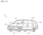
- FIG. 10 is an appearance diagram showing a configuration example of a vehicle that incorporates a vehicle-mounted apparatus.
- the vehicle X of the present configuration example includes vehicle-mounted apparatuses X 11 to X 17 and a battery (not shown) that supplies power to the vehicle-mounted apparatuses X 11 to X 17 .
- the vehicle-mounted apparatus X 11 is an engine control unit that performs control related to an engine (such as injection control, electronic throttle control, aiding control, oxygen sensor heater control and auto cruise control).
- control related to an engine such as injection control, electronic throttle control, aiding control, oxygen sensor heater control and auto cruise control.
- the vehicle-mounted apparatus X 12 is a lamp control unit that controls the turning on and off of a HID (high intensity discharged lamp), a DRL (daytime running lamp) and the like.
- the vehicle-mounted apparatus X 13 is a transmission control unit that performs control related to a transmission.
- the vehicle-mounted apparatus X 14 is a body control unit that performs control related to the movement of the vehicle X (such as ABS (anti-lock brake system) control, EPS (electric power steering) control and electronic suspension control).
- ABS anti-lock brake system
- EPS electric power steering
- the vehicle-mounted apparatus X 15 is a security control unit that performs drive control on a door lock, a burglar alarm and the like.
- the vehicle-mounted apparatus X 16 is an electronic apparatus that is incorporated in the vehicle X at the stage of factory shipment, as a standard accessory and a maker option such as a wiper, an electrically operated door mirror, a powered window, an electrically operated sunroof, an electrically operated sheet and an air-conditioner.
- the vehicle-mounted apparatus X 17 is an electronic apparatus with which the vehicle X is arbitrarily equipped by a user, such as a vehicle-mounted A/V (audio/visual) apparatus, a car navigation system and an ETC (electronic toll collection system).
- a vehicle-mounted A/V (audio/visual) apparatus such as a vehicle-mounted A/V (audio/visual) apparatus, a car navigation system and an ETC (electronic toll collection system).
- the power supply device 1 described previously can be incorporated in any of the vehicle-mounted apparatuses X 11 to X 17 .
- the power supply device having a first technical feature includes the control circuit that generates the on-time fixed pulse where the on-time and the on-time number are constant to turn on and off the output transistor, and thereby alternately repeats the operation period during which the charge is supplied to the coil and the still period during which the generation of the on-time fixed pulse is stopped, with the result that the output voltage is generated from the input voltage (1-1 configuration).
- the control circuit includes the on-time fixed pulse generation portion that generates the on-time fixed pulse each time all of charge supplied to the coil is consumed as the output current to the load (1-2 configuration).
- the control circuit includes the on-time fixed pulse adjustment portion that adjusts at least one of the on-time and the on-time number of the on-time fixed pulse (1-3 configuration).
- the on-time fixed pulse adjustment portion generates the on-time adjustment signal and the on-time number adjustment signal according to the external control signals input to the external terminals (1-4 configuration).
- the control circuit includes: the PWM pulse generation portion that generates the PWM pulse according to the output feedback control; the selector that selects any one of the on-time fixed pulse and the PWM pulse according to the weight of the load; and the drive that turns on and off the output transistor according to the output of the selector (1-5 configuration).
- the control circuit includes: the feedback voltage generation portion that generates the feedback voltage corresponding to the output voltage; the error amplifier that generates the error voltage corresponding to the difference between the predetermined reference voltage and the feedback voltage; and the comparator that generates the comparison signal corresponding to the result of the comparison between the predetermined slope voltage and the error voltage to output it to the PWM pulse generation portion (1-6 configuration).
- the on-time fixed pulse generation portion generates, when the pulse edge of the comparison signal is detected, the on-time fixed pulse and thereafter stops the generation of the on-time fixed pulse until the pulse edge of the comparison signal is subsequently detected (1-7 configuration).
- the control circuit includes the on-time fixed pulse cancellation portion that controls, when the input voltage is higher than the predetermined threshold voltage, the selector such that the PWM pulse is selected regardless of the weight of the load (1-8 configuration).
- the on-time fixed pulse cancellation portion controls, when the input voltage is lower than the threshold voltage, the selector such that any one of the PWM pulse and the on-time fixed pulse is selected (1-9 configuration).
- the vehicle-mounted apparatus disclosed in the present specification includes the power supply device of any one of the 1-1 to 1-9 configurations (1-10 configuration).
- the vehicle disclosed in the present specification includes the vehicle-mounted apparatus of the 1-10 configuration and the battery that supplies power to the vehicle-mounted apparatus (1-11 configuration).
- the power supply device having a second technical feature includes: a control circuit that turns on and off an output transistor to generate an output voltage from an input voltage; an internal power supply voltage generation circuit that generates an internal power supply voltage from an external power supply voltage; and a power switching circuit that switches supply of the internal power supply voltage and supply of the output voltage as a drive voltage of the control circuit (2-1 configuration).
- the control circuit includes a soft start voltage generation portion that generates a soft start voltage which starts to gently increase after the power supply device is started up, and the power switching circuit performs power switching control according to whether or not the soft start voltage exceeds a predetermined threshold voltage (2-2 configuration).
- the power switching circuit performs power switching control according to whether or not the output voltage or a feedback voltage corresponding to the output voltage falls within a normal range (2-3 configuration).
- the power switching circuit performs power switching control according to whether or not a state where the power supply device is forcibly stopped is cancelled (2-4 configuration).
- the soft start voltage generation portion uses a current source and a transistor connected in series to the current source and thereby performs charge and discharge control on a capacitor connected to a connection node between the current source and the transistor so as to control the soft start voltage (2-5 configuration).
- the soft start voltage generation portion turns on the transistor to discharge the soft start voltage when a forcible stop signal of the power supply device is input, and the power switching circuit performs, when the forcible stop signal is input, power switching such that the internal power supply voltage is supplied as the drive voltage of the control circuit (2-6 configuration).
- the control circuit includes a logical operation circuit to which a soft start completion signal, the forcible stop signal and an abnormal detection signal are input, and the power switching circuit performs, based on an output of the logical operation circuit, when soft start is completed, forcible stop is cancelled and abnormality is not detected, power switching such that the output voltage is supplied as the drive voltage of the control circuit (2-7 configuration).
- the power switching circuit performs power switching such that the internal power supply voltage is supplied as the drive voltage of the control circuit (2-8 configuration).
- the internal power supply voltage generation circuit includes: a pre-regulator circuit that generates an internal voltage from the external power supply voltage; and a reference voltage generation portion that receives the internal voltage generated by the pre-regulator circuit to generate a constant reference voltage used for the generation of the internal power supply voltage (2-9 configuration).
- the vehicle-mounted apparatus disclosed in the present specification includes the power supply device of any one of the 2-1 to 2-9 configurations (2-10 configuration).
- the vehicle disclosed in the present specification includes the vehicle-mounted apparatus of the 2-10 configuration and the battery that supplies power to the vehicle-mounted apparatus (2-11 configuration).
- the power supply device having a third technical feature includes: an output transistor that is turned on and off to generate an output voltage from an input voltage; a feedback voltage generation portion that generates a feedback voltage corresponding to the out voltage; a soft start voltage generation portion that generates a soft start voltage which gently increases when the power supply device is started up; an error amplifier that generates an error voltage corresponding to a difference between which of a predetermined reference voltage and the soft start voltage is lower and the feedback voltage; an oscillator that generates a clock signal of a predetermined frequency; a slope voltage generation portion that generates a slope voltage in synchronization with the clock signal; a comparator that compares the error voltage and the slope voltage to generate a comparison signal; a PWM pulse generation portion that generates a PWM pulse based on the clock signal and the comparison signal; an on-time fixed pulse generation portion that uses the comparison signal as a trigger to generate an on-time fixed pulse where an on-time and an on-time number are constant; a
- the power supply device of the 3-1 configuration further includes a selector control portion that generates a selector control signal such that any one of the PWM pulse and the on-time fixed pulse is selected according to the weight of a load (3-2 configuration).
- the selector selects the one shot pulse regardless of the selector control signal when the soft start voltage exceeds the threshold voltage (3-3 configuration).
- the selector control portion monitors a period during which the comparison signal is kept at the same logic level to determine the weight of the load (3-4 configuration).
- the on-time of the PWM pulse is a minimum on-time (3-5 configuration).
- the selector control portion when the load is further reduced in the PWM mode, the switch voltage is brought from the discontinuous mode to an intermittent oscillation mode and the comparison signal is kept at the same logic level over a predetermined mask period, the selector control portion generates the selector control signal such that the mode is brought to an on-time fixed mode where the selector selects the on-time fixed pulse (3-6 configuration).
- the power supply device of the 3-6 configuration further includes a counter adjustment portion that generates a mask period adjustment signal for adjusting the mask period according to an external control signal input to an external terminal, and that feeds out the mask period adjustment signal to the selector control portion (3-7 configuration).
- the soft start voltage generation portion detects that the soft start exceeds the threshold voltage to generate a soft start completion signal, and the one shot pulse generation portion uses an edge of the soft start completion signal as a trigger to generate the one shot pulse (3-8 configuration).
- the vehicle-mounted apparatus disclosed in the present specification includes the power supply device of any one of the 3-1 to 3-8 configurations (3-9 configuration).
- the vehicle disclosed in the present specification includes the vehicle-mounted apparatus of the 3-9 configuration and the battery that supplies power to the vehicle-mounted apparatus (3-10 configuration).
- the power supply device having a fourth technical feature includes: an output transistor that is turned on and off to generate an output voltage from an input voltage; a feedback voltage generation portion that generates a feedback voltage corresponding to the out voltage; an error amplifier that generates an error voltage corresponding to a difference between a predetermined reference voltage and the feedback voltage; an oscillator that generates a clock signal of a predetermined frequency; a slope voltage generation portion that generates a slope voltage in synchronization with the clock signal; a comparator that compares the error voltage and the slope voltage to generate a comparison signal; a PWM pulse generation portion that generates a PWM pulse based on the clock signal and the comparison signal; an on-time fixed pulse generation portion that uses the comparison signal as a trigger to generate an on-time fixed pulse where an on-time and an on-time number are constant; a selector that selects any one of the PWM pulse and the on-time fixed pulse; a driver that turns on and off the output transistor according to an output of
- the comparison signal is such a binary signal that the comparison signal is low when the error voltage is higher than the slope voltage whereas the comparison signal is high when the error voltage is lower than the slope voltage
- the selector control portion includes a counter that measures a period during which the comparison signal is low (4-2 configuration).
- the selector control portion generates, when the period during which the comparison signal is low is shorter than the mask period, the control signal so as to select the PWM pulse whereas the selector control portion generates, when the period during which the comparison signal is low is longer than the mask period, the control signal so as to select the on-time fixed pulse (4-3 configuration).
- the mask period is longer than a pulse period of the clock signal (4-4 configuration).
- the power supply device of the 4-4 configuration further includes a counter adjustment portion that adjusts the mask period (4-5 configuration).
- a first threshold current when a PWM mode where the PWM pulse is selected is switched to an on-time fixed mode where the on-time fixed pulse is selected is determined by charge that is supplied to a load each time the output transistor is turned on in the PWM mode and a switching period in the PWM mode at a time of a light load (4-6 configuration).
- a second threshold current when an on-time fixed mode where the on-time fixed pulse is selected is switched to a PWM mode where the PWM pulse is selected is determined by charge that is supplied to a load each time the output transistor is turned on N times in the on-time fixed mode and an on-time of each of the on-time fixed pulses (4-7 configuration).
- the second threshold current is expressed by N ⁇ Q/Tmask (where N is an on-time number of the on-time fixed pulse, Q is charge that is supplied to the load each time the output transistor is turned on and Tmask is the mask period (4-8 configuration).
- the counter adjustment portion generates a mask period adjustment signal which adjusts the mask period according to an external control signal input from an external terminal and feeds out the mask period adjustment signal to the selector control portion (4-9 configuration).
- the vehicle-mounted apparatus disclosed in the present specification includes the power supply device of any one of the 4-1 to 4-9 configurations (4-10 configuration).
- the vehicle disclosed in the present specification includes the vehicle-mounted apparatus of the 4-10 configuration and the battery that supplies power to the vehicle-mounted apparatus (4-11 configuration).
- the present invention can be applied to, for example, a vehicle-mounted power supply device.
Applications Claiming Priority (2)
| Application Number | Priority Date | Filing Date | Title |
|---|---|---|---|
| JP2012-137680 | 2012-06-19 | ||
| JP2012137680A JP2014003812A (ja) | 2012-06-19 | 2012-06-19 | 電源装置、並びに、これを用いた車載機器及び車両 |
Publications (2)
| Publication Number | Publication Date |
|---|---|
| US20130334876A1 US20130334876A1 (en) | 2013-12-19 |
| US9541928B2 true US9541928B2 (en) | 2017-01-10 |
Family
ID=49755223
Family Applications (1)
| Application Number | Title | Priority Date | Filing Date |
|---|---|---|---|
| US13/920,465 Active 2035-04-12 US9541928B2 (en) | 2012-06-19 | 2013-06-18 | Power supply device, and vehicle-mounted apparatus and vehicle using same |
Country Status (2)
| Country | Link |
|---|---|
| US (1) | US9541928B2 (ja) |
| JP (1) | JP2014003812A (ja) |
Cited By (1)
| Publication number | Priority date | Publication date | Assignee | Title |
|---|---|---|---|---|
| US11515788B2 (en) * | 2018-03-22 | 2022-11-29 | Rohm Co., Ltd. | Switching control circuit |
Families Citing this family (6)
| Publication number | Priority date | Publication date | Assignee | Title |
|---|---|---|---|---|
| US9391551B2 (en) * | 2013-06-28 | 2016-07-12 | Stmicroelectronics S.R.L. | Apparatus to detect the zero-cross of the BEMF of a three-phase electric motor and related method |
| CN107005159B (zh) * | 2014-12-19 | 2019-10-18 | 索尼公司 | 电压转换电路、电子装置以及电压转换电路的控制方法 |
| JP6407071B2 (ja) * | 2015-03-16 | 2018-10-17 | 株式会社東芝 | 電圧切替回路および電源装置 |
| JP6581443B2 (ja) * | 2015-09-04 | 2019-09-25 | 日立オートモティブシステムズ株式会社 | センサ装置 |
| CN107317476B (zh) * | 2017-07-19 | 2019-11-12 | 深圳市华星光电半导体显示技术有限公司 | 输出电压调整电路及液晶显示装置 |
| US11095282B2 (en) * | 2018-12-05 | 2021-08-17 | Texas Instruments Incorporated | Methods and apparatus to implement current limit test mode |
Citations (22)
| Publication number | Priority date | Publication date | Assignee | Title |
|---|---|---|---|---|
| US5986632A (en) | 1994-10-31 | 1999-11-16 | Semiconductor Energy Laboratory Co., Ltd. | Active matrix type flat-panel display device |
| US6452368B1 (en) * | 2000-10-19 | 2002-09-17 | Semiconductor Components Industries Llc | Circuit and method of operating a low-noise, on-demand regulator in switched or linear mode |
| US20050057238A1 (en) * | 2002-07-11 | 2005-03-17 | Yutaka Yoshida | DC-DC converter |
| US20060202669A1 (en) | 2005-03-10 | 2006-09-14 | Fujitsu Limited | Control circuit and control method of current mode control type DC-DC converter |
| US20070090774A1 (en) | 2005-10-25 | 2007-04-26 | Hon Hai Precision Industry Co., Ltd. | Discharge lamp driving device and driving method |
| US20080094048A1 (en) * | 2005-07-15 | 2008-04-24 | Christophe Basso | Power Supply Controller And Method Therefor |
| US7405549B2 (en) * | 2005-08-05 | 2008-07-29 | Rohm Co., Ltd. | Soft start circuit, power supply unit and electric equipment |
| US20080259655A1 (en) * | 2007-04-19 | 2008-10-23 | Da-Chun Wei | Switching-mode power converter and pulse-width-modulation control circuit with primary-side feedback control |
| US20090218999A1 (en) * | 2008-03-03 | 2009-09-03 | Nec Electronics Corporation | DC converter which has switching control unit to select PWM signal or PFM signal |
| US20090237049A1 (en) * | 2006-11-28 | 2009-09-24 | Thine Electronics, Inc. | Comparator type dc-dc converter |
| US20090315523A1 (en) | 2008-06-20 | 2009-12-24 | Mitsumi Electric Co., Ltd. | Dc-dc converter |
| JP2010081749A (ja) | 2008-09-26 | 2010-04-08 | Fujitsu Microelectronics Ltd | Dc−dcコンバータの制御回路、およびdc−dcコンバータの制御方法 |
| US20100225288A1 (en) * | 2009-03-05 | 2010-09-09 | Richtek Technology Corporation, R.O.C. | Multi-phase power converter and control circuit and method thereof |
| US20100225293A1 (en) | 2009-03-05 | 2010-09-09 | Iwatt Inc. | Adaptive control for transition between multiple modulation modes in a switching power converter |
| JP2011061971A (ja) | 2009-09-10 | 2011-03-24 | Fujitsu Semiconductor Ltd | オン時間固定方式dc−dcコンバータ |
| US20110169471A1 (en) * | 2010-01-14 | 2011-07-14 | Renesas Electronics Corporation | Semiconductor device and power source device |
| US20120019225A1 (en) * | 2010-07-26 | 2012-01-26 | Richtek Technology Corporation, R.O.C. | Control circuit and method for reducing output ripple in constant on-time switching regulator |
| US20120038341A1 (en) | 2009-04-27 | 2012-02-16 | Yuusuke Michishita | Switching regulator and operation control method thereof |
| US8319487B2 (en) | 2008-09-04 | 2012-11-27 | Ricoh Company, Ltd. | Non-isolated current-mode-controlled switching voltage regulator |
| US20130093407A1 (en) | 2011-10-12 | 2013-04-18 | Electronics And Telecommunications Research Institute | Dc-dc converter |
| US20130334877A1 (en) | 2012-06-19 | 2013-12-19 | Rohm Co., Ltd. | Power supply device, and vehicle-mounted apparatus and vehicle using same |
| US20140084886A1 (en) | 2012-09-27 | 2014-03-27 | Olivier Causse | Converter and method |
-
2012
- 2012-06-19 JP JP2012137680A patent/JP2014003812A/ja active Pending
-
2013
- 2013-06-18 US US13/920,465 patent/US9541928B2/en active Active
Patent Citations (22)
| Publication number | Priority date | Publication date | Assignee | Title |
|---|---|---|---|---|
| US5986632A (en) | 1994-10-31 | 1999-11-16 | Semiconductor Energy Laboratory Co., Ltd. | Active matrix type flat-panel display device |
| US6452368B1 (en) * | 2000-10-19 | 2002-09-17 | Semiconductor Components Industries Llc | Circuit and method of operating a low-noise, on-demand regulator in switched or linear mode |
| US20050057238A1 (en) * | 2002-07-11 | 2005-03-17 | Yutaka Yoshida | DC-DC converter |
| US20060202669A1 (en) | 2005-03-10 | 2006-09-14 | Fujitsu Limited | Control circuit and control method of current mode control type DC-DC converter |
| US20080094048A1 (en) * | 2005-07-15 | 2008-04-24 | Christophe Basso | Power Supply Controller And Method Therefor |
| US7405549B2 (en) * | 2005-08-05 | 2008-07-29 | Rohm Co., Ltd. | Soft start circuit, power supply unit and electric equipment |
| US20070090774A1 (en) | 2005-10-25 | 2007-04-26 | Hon Hai Precision Industry Co., Ltd. | Discharge lamp driving device and driving method |
| US20090237049A1 (en) * | 2006-11-28 | 2009-09-24 | Thine Electronics, Inc. | Comparator type dc-dc converter |
| US20080259655A1 (en) * | 2007-04-19 | 2008-10-23 | Da-Chun Wei | Switching-mode power converter and pulse-width-modulation control circuit with primary-side feedback control |
| US20090218999A1 (en) * | 2008-03-03 | 2009-09-03 | Nec Electronics Corporation | DC converter which has switching control unit to select PWM signal or PFM signal |
| US20090315523A1 (en) | 2008-06-20 | 2009-12-24 | Mitsumi Electric Co., Ltd. | Dc-dc converter |
| US8319487B2 (en) | 2008-09-04 | 2012-11-27 | Ricoh Company, Ltd. | Non-isolated current-mode-controlled switching voltage regulator |
| JP2010081749A (ja) | 2008-09-26 | 2010-04-08 | Fujitsu Microelectronics Ltd | Dc−dcコンバータの制御回路、およびdc−dcコンバータの制御方法 |
| US20100225288A1 (en) * | 2009-03-05 | 2010-09-09 | Richtek Technology Corporation, R.O.C. | Multi-phase power converter and control circuit and method thereof |
| US20100225293A1 (en) | 2009-03-05 | 2010-09-09 | Iwatt Inc. | Adaptive control for transition between multiple modulation modes in a switching power converter |
| US20120038341A1 (en) | 2009-04-27 | 2012-02-16 | Yuusuke Michishita | Switching regulator and operation control method thereof |
| JP2011061971A (ja) | 2009-09-10 | 2011-03-24 | Fujitsu Semiconductor Ltd | オン時間固定方式dc−dcコンバータ |
| US20110169471A1 (en) * | 2010-01-14 | 2011-07-14 | Renesas Electronics Corporation | Semiconductor device and power source device |
| US20120019225A1 (en) * | 2010-07-26 | 2012-01-26 | Richtek Technology Corporation, R.O.C. | Control circuit and method for reducing output ripple in constant on-time switching regulator |
| US20130093407A1 (en) | 2011-10-12 | 2013-04-18 | Electronics And Telecommunications Research Institute | Dc-dc converter |
| US20130334877A1 (en) | 2012-06-19 | 2013-12-19 | Rohm Co., Ltd. | Power supply device, and vehicle-mounted apparatus and vehicle using same |
| US20140084886A1 (en) | 2012-09-27 | 2014-03-27 | Olivier Causse | Converter and method |
Non-Patent Citations (1)
| Title |
|---|
| USPTO, communication in U.S. Appl. No. 13/920,517 (dated Dec. 21, 2015). |
Cited By (1)
| Publication number | Priority date | Publication date | Assignee | Title |
|---|---|---|---|---|
| US11515788B2 (en) * | 2018-03-22 | 2022-11-29 | Rohm Co., Ltd. | Switching control circuit |
Also Published As
| Publication number | Publication date |
|---|---|
| US20130334876A1 (en) | 2013-12-19 |
| JP2014003812A (ja) | 2014-01-09 |
Similar Documents
| Publication | Publication Date | Title |
|---|---|---|
| US9182769B2 (en) | Power supply device, and vehicle-mounted apparatus and vehicle using same | |
| US9541928B2 (en) | Power supply device, and vehicle-mounted apparatus and vehicle using same | |
| US11398771B2 (en) | Switching regulator control circuit enabling fault protection operation, current-mode-control switching power supply device, and vehicle | |
| US9030177B2 (en) | Switched-mode power supply having an adaptive on-time function and controlling output with a ripple control method | |
| US7145316B1 (en) | Control circuit for monitoring and maintaining a bootstrap voltage in an N-channel buck regulator | |
| US7804285B2 (en) | Control of operation of switching regulator to select PWM control or PFM control based on phase comparison | |
| US8872497B2 (en) | Switched-mode power supply | |
| JP3647811B2 (ja) | Dc−dcコンバータ回路 | |
| JP5091028B2 (ja) | スイッチングレギュレータ及びそのスイッチングレギュレータを備えた半導体装置 | |
| US20070120548A1 (en) | Switching regulator, and a circuit and method for controlling the switching regulator | |
| US20090174384A1 (en) | Switching regulator and method of controlling the same | |
| US20090322299A1 (en) | Non-isolated current-mode-controlled switching voltage regulator | |
| US9429963B2 (en) | Power supply device, and vehicle-mounted apparatus and vehicle using same | |
| US10218269B2 (en) | Switching regulator and integrated-circuit package | |
| US10298130B2 (en) | Switching regulator | |
| US9698696B2 (en) | Insulation type switching power supply apparatus | |
| US20120299569A1 (en) | Constant On-Time Switching Regulator Implementing Light Load Control | |
| JP6154584B2 (ja) | 電源装置、並びに、これを用いた車載機器及び車両 | |
| JP6101439B2 (ja) | 電源装置、並びに、これを用いた車載機器及び車両 | |
| JP2014003770A (ja) | 電源装置、並びに、これを用いた車載機器及び車両 | |
| US8324873B2 (en) | Power supply apparatus and power supply method | |
| JP2017121164A (ja) | スイッチングレギュレータ | |
| US20130106384A1 (en) | Voltage converting circuit |
Legal Events
| Date | Code | Title | Description |
|---|---|---|---|
| AS | Assignment |
Owner name: ROHM CO., LTD., JAPAN Free format text: ASSIGNMENT OF ASSIGNORS INTEREST;ASSIGNOR:YAMAGUCHI, YUHEI;REEL/FRAME:030640/0255 Effective date: 20130604 |
|
| STCF | Information on status: patent grant |
Free format text: PATENTED CASE |
|
| MAFP | Maintenance fee payment |
Free format text: PAYMENT OF MAINTENANCE FEE, 4TH YEAR, LARGE ENTITY (ORIGINAL EVENT CODE: M1551); ENTITY STATUS OF PATENT OWNER: LARGE ENTITY Year of fee payment: 4 |