US9461116B2 - Method of formation of a TI-IGBT - Google Patents
Method of formation of a TI-IGBT Download PDFInfo
- Publication number
- US9461116B2 US9461116B2 US14/649,553 US201214649553A US9461116B2 US 9461116 B2 US9461116 B2 US 9461116B2 US 201214649553 A US201214649553 A US 201214649553A US 9461116 B2 US9461116 B2 US 9461116B2
- Authority
- US
- United States
- Prior art keywords
- semiconductor substrate
- doped layer
- igbt
- region
- forming
- Prior art date
- Legal status (The legal status is an assumption and is not a legal conclusion. Google has not performed a legal analysis and makes no representation as to the accuracy of the status listed.)
- Expired - Fee Related
Links
Images


Classifications
-
- H01L29/0834—
-
- H—ELECTRICITY
- H10—SEMICONDUCTOR DEVICES; ELECTRIC SOLID-STATE DEVICES NOT OTHERWISE PROVIDED FOR
- H10D—INORGANIC ELECTRIC SEMICONDUCTOR DEVICES
- H10D62/00—Semiconductor bodies, or regions thereof, of devices having potential barriers
- H10D62/10—Shapes, relative sizes or dispositions of the regions of the semiconductor bodies; Shapes of the semiconductor bodies
- H10D62/13—Semiconductor regions connected to electrodes carrying current to be rectified, amplified or switched, e.g. source or drain regions
- H10D62/141—Anode or cathode regions of thyristors; Collector or emitter regions of gated bipolar-mode devices, e.g. of IGBTs
- H10D62/142—Anode regions of thyristors or collector regions of gated bipolar-mode devices
-
- H—ELECTRICITY
- H01—ELECTRIC ELEMENTS
- H01L—SEMICONDUCTOR DEVICES NOT COVERED BY CLASS H10
- H01L21/00—Processes or apparatus adapted for the manufacture or treatment of semiconductor or solid state devices or of parts thereof
- H01L21/02—Manufacture or treatment of semiconductor devices or of parts thereof
- H01L21/04—Manufacture or treatment of semiconductor devices or of parts thereof the devices having potential barriers, e.g. a PN junction, depletion layer or carrier concentration layer
- H01L21/18—Manufacture or treatment of semiconductor devices or of parts thereof the devices having potential barriers, e.g. a PN junction, depletion layer or carrier concentration layer the devices having semiconductor bodies comprising elements of Group IV of the Periodic Table or AIIIBV compounds with or without impurities, e.g. doping materials
- H01L21/26—Bombardment with radiation
- H01L21/263—Bombardment with radiation with high-energy radiation
- H01L21/265—Bombardment with radiation with high-energy radiation producing ion implantation
- H01L21/26506—Bombardment with radiation with high-energy radiation producing ion implantation in group IV semiconductors
- H01L21/26513—Bombardment with radiation with high-energy radiation producing ion implantation in group IV semiconductors of electrically active species
-
- H—ELECTRICITY
- H01—ELECTRIC ELEMENTS
- H01L—SEMICONDUCTOR DEVICES NOT COVERED BY CLASS H10
- H01L21/00—Processes or apparatus adapted for the manufacture or treatment of semiconductor or solid state devices or of parts thereof
- H01L21/02—Manufacture or treatment of semiconductor devices or of parts thereof
- H01L21/04—Manufacture or treatment of semiconductor devices or of parts thereof the devices having potential barriers, e.g. a PN junction, depletion layer or carrier concentration layer
- H01L21/18—Manufacture or treatment of semiconductor devices or of parts thereof the devices having potential barriers, e.g. a PN junction, depletion layer or carrier concentration layer the devices having semiconductor bodies comprising elements of Group IV of the Periodic Table or AIIIBV compounds with or without impurities, e.g. doping materials
- H01L21/30—Treatment of semiconductor bodies using processes or apparatus not provided for in groups H01L21/20 - H01L21/26
- H01L21/302—Treatment of semiconductor bodies using processes or apparatus not provided for in groups H01L21/20 - H01L21/26 to change their surface-physical characteristics or shape, e.g. etching, polishing, cutting
-
- H01L29/0615—
-
- H01L29/0821—
-
- H01L29/36—
-
- H01L29/66333—
-
- H01L29/7395—
-
- H—ELECTRICITY
- H10—SEMICONDUCTOR DEVICES; ELECTRIC SOLID-STATE DEVICES NOT OTHERWISE PROVIDED FOR
- H10D—INORGANIC ELECTRIC SEMICONDUCTOR DEVICES
- H10D12/00—Bipolar devices controlled by the field effect, e.g. insulated-gate bipolar transistors [IGBT]
- H10D12/01—Manufacture or treatment
- H10D12/031—Manufacture or treatment of IGBTs
- H10D12/032—Manufacture or treatment of IGBTs of vertical IGBTs
-
- H—ELECTRICITY
- H10—SEMICONDUCTOR DEVICES; ELECTRIC SOLID-STATE DEVICES NOT OTHERWISE PROVIDED FOR
- H10D—INORGANIC ELECTRIC SEMICONDUCTOR DEVICES
- H10D12/00—Bipolar devices controlled by the field effect, e.g. insulated-gate bipolar transistors [IGBT]
- H10D12/411—Insulated-gate bipolar transistors [IGBT]
- H10D12/441—Vertical IGBTs
-
- H—ELECTRICITY
- H10—SEMICONDUCTOR DEVICES; ELECTRIC SOLID-STATE DEVICES NOT OTHERWISE PROVIDED FOR
- H10D—INORGANIC ELECTRIC SEMICONDUCTOR DEVICES
- H10D62/00—Semiconductor bodies, or regions thereof, of devices having potential barriers
- H10D62/10—Shapes, relative sizes or dispositions of the regions of the semiconductor bodies; Shapes of the semiconductor bodies
- H10D62/13—Semiconductor regions connected to electrodes carrying current to be rectified, amplified or switched, e.g. source or drain regions
- H10D62/137—Collector regions of BJTs
-
- H—ELECTRICITY
- H10—SEMICONDUCTOR DEVICES; ELECTRIC SOLID-STATE DEVICES NOT OTHERWISE PROVIDED FOR
- H10D—INORGANIC ELECTRIC SEMICONDUCTOR DEVICES
- H10D62/00—Semiconductor bodies, or regions thereof, of devices having potential barriers
- H10D62/60—Impurity distributions or concentrations
-
- H10P30/204—
-
- H10P30/21—
-
- H10P50/00—
-
- H—ELECTRICITY
- H01—ELECTRIC ELEMENTS
- H01L—SEMICONDUCTOR DEVICES NOT COVERED BY CLASS H10
- H01L21/00—Processes or apparatus adapted for the manufacture or treatment of semiconductor or solid state devices or of parts thereof
- H01L21/02—Manufacture or treatment of semiconductor devices or of parts thereof
- H01L21/04—Manufacture or treatment of semiconductor devices or of parts thereof the devices having potential barriers, e.g. a PN junction, depletion layer or carrier concentration layer
- H01L21/18—Manufacture or treatment of semiconductor devices or of parts thereof the devices having potential barriers, e.g. a PN junction, depletion layer or carrier concentration layer the devices having semiconductor bodies comprising elements of Group IV of the Periodic Table or AIIIBV compounds with or without impurities, e.g. doping materials
- H01L21/185—Joining of semiconductor bodies for junction formation
-
- H—ELECTRICITY
- H10—SEMICONDUCTOR DEVICES; ELECTRIC SOLID-STATE DEVICES NOT OTHERWISE PROVIDED FOR
- H10D—INORGANIC ELECTRIC SEMICONDUCTOR DEVICES
- H10D62/00—Semiconductor bodies, or regions thereof, of devices having potential barriers
- H10D62/10—Shapes, relative sizes or dispositions of the regions of the semiconductor bodies; Shapes of the semiconductor bodies
- H10D62/102—Constructional design considerations for preventing surface leakage or controlling electric field concentration
- H10D62/103—Constructional design considerations for preventing surface leakage or controlling electric field concentration for increasing or controlling the breakdown voltage of reverse-biased devices
- H10D62/105—Constructional design considerations for preventing surface leakage or controlling electric field concentration for increasing or controlling the breakdown voltage of reverse-biased devices by having particular doping profiles, shapes or arrangements of PN junctions; by having supplementary regions, e.g. junction termination extension [JTE]
-
- H10P10/12—
Definitions
- the present disclosure relates to the technical field of semiconductor device fabrication, and particularly to a TI-IGBT and a formation method thereof.
- IGBT Insulated Gate Bipolar Transistor
- BJT Bipolar Junction Transistor
- MOSFET Insulated Gate Field Effect Transistor
- TI-IGBT Triple mode Integrate Insulated Gate Bipolar Transistor
- the TI-IGBT device has small conduction voltage drop in the case that the TI-IGBT device is forward turned on, similarly to IGBT; the TI-IGBT device has a fast turn-off speed in the case that the TI-IGBT device is turned off, similarly to VDMOS; and it is not necessary to connect a fast recover diode in anti-parallel in the case that a reverse voltage is applied on the TI-IGBT device, similarly to FRD.
- TI-IGBT device has small conduction voltage drop in the case that the TI-IGBT device is forward turned on, similarly to IGBT; the TI-IGBT device has a fast turn-off speed in the case that the TI-IGBT device is turned off, similarly to VDMOS; and it is not necessary to connect a fast recover diode in anti-parallel in the case that a reverse voltage is applied on the TI-IGBT device, similarly to FRD.
- a TI-IGBT includes: a first semiconductor substrate, where a short-circuit region and a collector region disposed in parallel are formed in the first semiconductor substrate, and a doping type of the short-circuit region is different from a doping type of the collector region; a second semiconductor substrate, where the second semiconductor substrate is located above an upper surface of the first semiconductor substrate, and a doping type of the second semiconductor substrate is the same as the doping type of the short-circuit region; and a first doped layer, where the first doped layer is located between the first semiconductor substrate and the second semiconductor substrate, and the first doped layer covers at least the collector region in the first semiconductor substrate, where a doping type of the first doped layer is the same as the doping type of the second semiconductor substrate, and a doping concentration of the first doped layer is lower than a doping concentration of the second semiconductor substrate.
- the first semiconductor substrate is covered completely by the first doped layer.
- only the collector region is covered by the first doped layer.
- the TI-IGBT further includes a second doped layer, where the second doped layer is located between the short-circuit region and the second semiconductor substrate, and a doping type of the second doped layer is the same as the doping type of the second semiconductor substrate, and a doping concentration of the second doped layer is higher than the doping concentration of the second semiconductor substrate.
- the first doped layer has a thickness of 1 ⁇ m to 10 ⁇ m, inclusive.
- the first doped layer has a doping concentration of 10 12 ⁇ cm ⁇ 3 to 10 13 ⁇ cm ⁇ 3 , inclusive.
- the TI-IGBT is a punch-through TI-IGBT
- the TI-IGBT further includes a buffer layer located between the first doped layer and the second semiconductor substrate, where a doping type of the buffer layer is the same as the doping type of the second semiconductor substrate and a doping concentration of the buffer layer is higher than the doping concentration of the second semiconductor substrate.
- a formation method of a TI-IGBT includes: providing a first semiconductor substrate; forming a first doped layer on an upper surface of the first semiconductor substrate; forming a second semiconductor substrate above the first semiconductor substrate, where the second semiconductor substrate completely covers the first doped layer and the first semiconductor substrate; and forming a short-circuit region and a collector region disposed in parallel in the first semiconductor substrate, where the first doped layer covers at least the collector region, a doping type of the first doped layer is the same as a doping type of the second semiconductor substrate, and a doping concentration of the first doped layer is lower than a doping concentration of the second semiconductor substrate.
- the first doped layer completely covers the first semiconductor substrate.
- the first doped layer covers only the collector region.
- the formation method further includes forming a second doped layer on an upper surface of the short-circuit region before forming the second semiconductor substrate above the first semiconductor substrate, where a doping type of the second doped layer is the same as the doping type of the second semiconductor substrate, and a doping concentration of the second doped layer is higher than the doping concentration of the second semiconductor substrate.
- forming the short-circuit region and the collector region disposed in parallel in the first semiconductor substrate includes: thinning a lower surface of the first semiconductor substrate; forming the collector region by implanting P-type ions into a part of the first semiconductor substrate where the collector region is to be formed; and forming the short-circuit region by implanting N-type ions into a part of the first semiconductor substrate where the short-circuit region is to be formed.
- forming the short-circuit region and the collector region disposed in parallel in the first semiconductor substrate includes: thinning a lower surface of the first semiconductor substrate; forming the collector region by implanting P-type ions into the first semiconductor substrate; removing a part of the collector region in the first semiconductor region where the short-circuit region is to be formed; and forming the short-circuit region by implanting N-type ions into a part of the first semiconductor substrate where the short-circuit region is to be formed.
- the first semiconductor substrate is a P-type semiconductor substrate
- forming the short-circuit region and the collector region disposed in parallel in the first semiconductor substrate includes: thinning a lower surface of the first semiconductor substrate; and forming the short-circuit region by implanting N-type ions into a part of the first semiconductor substrate where the short-circuit region is to be formed, where a part of the first semiconductor substrate where the ions are not implanted is the collector region.
- the first semiconductor substrate is an N-type semiconductor substrate
- forming the short-circuit region and the collector region disposed in parallel in the first semiconductor substrate includes: thinning a lower surface of the first semiconductor substrate; forming the collector region by implanting P-type ions into a part of the first semiconductor substrate where the collector region is to be formed, where a part of the first semiconductor substrate where the ions are not implanted is the short-circuit region.
- a formation method of a TI-IGBT includes: providing a first semiconductor substrate; forming a first doped layer on an upper surface of the first semiconductor substrate; forming a second semiconductor substrate above the first semiconductor substrate, where the second semiconductor substrate completely covers the first doped layer and the first semiconductor substrate; thinning a lower surface of the first semiconductor substrate to expose the first doped layer; and forming a short-circuit region and a collector region disposed in parallel in the first doped layer, where the first doped layer covers at least the collector region, a doping type of the first doped layer is the same as a doping type of the second semiconductor substrate, and a doping concentration of the first doped layer is lower than a doping concentration of the second semiconductor substrate.
- the formation method further includes forming a buffer layer above the first doped layer before forming the second semiconductor substrate above the first semiconductor substrate, where the buffer layer completely covers the first doped layer and the first semiconductor substrate, where a doping type of the buffer layer is the same as the doping type of the second semiconductor substrate, and a doping concentration of the buffer layer is higher than the doping concentration of the second semiconductor substrate.
- a first doped layer between the first semiconductor substrate and the second semiconductor substrate is added, with the doping type of the first doped layer being the same as that of the second semiconductor substrate and the doping concentration of the first doped layer being lower than that of the second semiconductor substrate, and thus the resistance above the collector region in the first semiconductor substrate is increased. Therefore, compared with the TI-IGBT in the conventional technology, a voltage drop across the same distance above the collector region is increased under a certain current density in the TI-IGBT according to the present disclosure, such that the TI-IGBT enters into an IGBT mode at a smaller current, thereby solving the current snap-back phenomenon during the operation of the TI-IGBT in the conventional technology.
- FIG. 1 is a schematic structural diagram of a VDMOS device in the conventional technology
- FIG. 2 is a schematic structural diagram of an IGBT device in the conventional technology
- FIG. 3 is a schematic structural diagram of a TI-IGBT device in the conventional technology
- FIG. 4 is a schematic graph of an I-V characteristic curve of a TI-IGBT device in the conventional technology
- FIG. 5 is a schematic diagram of a principle of current snap-back of a TI-IGBT device in the conventional technology
- FIG. 6 is a schematic structural diagram of a TI-IGBT according to the present disclosure.
- FIG. 7 is another schematic structural diagram of a TI-IGBT according to the present disclosure.
- FIG. 8 is still another schematic structural diagram of a TI-IGBT according to the present disclosure.
- FIGS. 9-15 are diagrams related to the process of the formation of TI-IGBT.
- the TI-IGBT device includes:
- a semiconductor substrate a front structure 20 formed on a front surface of the semiconductor substrate and a collector structure 30 formed on a rear surface of the semiconductor substrate.
- the part of the semiconductor substrate other than the parts of the front structure 20 and the collector structure 30 is a drift region 10 .
- the front structure 20 includes a gate structure 201 located on a surface of the semiconductor substrate and an emitter structure 202 located on both sides of the gate structure 201 .
- the gate structure 201 includes a gate dielectric layer 2011 formed on the surface of the semiconductor substrate and a gate electrode layer 2012 located on a surface of the gate dielectric layer 2011 .
- the emitter structure 202 includes an emitter 2021 formed on both sides of the gate structure 201 and in the semiconductor substrate and an emitter electrode 2022 formed on a surface of the emitter 2021 and electrically connected with the emitter 2021 .
- the collector structure 30 includes a collector region 301 and a short-circuit region 302 disposed in parallel on the rear surface of the semiconductor substrate and a collector 303 formed on the surfaces of the collector region 301 and the short-circuit region 302 and electrically connected with the collector region 301 and the short-circuit region 302 .
- the TI-IGBT device further includes a buffer layer 40 located between the collector structure 30 and the drift region 10 .
- the doping type of the buffer layer 40 is the same as that of the drift region 10 and the doping concentration of the buffer layer 40 is higher than that of the drift region 10 .
- the inventor has found through research that, at the early stage of the conduction of the TI-IGBT device, the current of the TI-IGBT device is small and the voltage V CE between the gate structure 201 and the collector structure 30 is large, as shown in FIG. 4 .
- the voltage V CE between the gate structure 201 and the collector structure 30 of the TI-IGBT device is larger than a specific value V p , the voltage V CE between the gate structure 201 and the collector structure 30 rapidly decreases and the current rapidly increases, that is, a current snap-back phenomenon occurs.
- the inventor has further found through research that, in the case of a punch through TI-IGBT device, as shown in FIG. 5 , at the early stage of the conduction, the TI-IGBT device operates in a VDMOS mode and is in unipolar conduction, electrons are injected into the drift region 10 from a channel region and then flow towards the buffer layer 40 in a nearly vertical direction; after the electrons are gathered together in the buffer layer 40 , the electrons above the collector region 301 flow to the above of the short-circuit region 302 in a horizontal direction and then flow out of the collector structure 30 through the short-circuit region 302 , and thus the electric potential above the collector region 301 gradually decreases in a direction from the edge of the collector region 301 to the center of the collector region 301 .
- Whether a collector junction of the punch-through TI-IGBT device is turned on depends on the electric potential above the collector region 301 .
- the current density is small.
- the electric potentials on both sides of the collector junction are smaller than a built-in electric potential of the collector junction, that is, Vmg ⁇ Vmf ⁇ . . . ⁇ Vma ⁇ 0.7V, such that the voltage drop generated above the collector region 301 is not sufficient to turn on the collector junction, and thus no hole is injected into one side of the collector region 301 .
- the conductivity modulation effect does not occur inside the punch-through TI-IGBT device, such that the conduction voltage drop of the punch-through TI-IGBT device is large, that is, the voltage V CE between the gate structure 201 and the collector structure 30 is large.
- the current density and the forward bias voltage of the collector junction increase as the voltage applied between the gate structure 201 and the collector structure 30 increases, as shown in FIG. 5 ( b ) , the collector junction starts to be turned on in the case that the voltage applied between the gate structure 201 and the collector structure 30 reaches a specific voltage value V p .
- Vmg ⁇ . . . ⁇ Vmd ⁇ 0.7V ⁇ Vmc ⁇ . . . ⁇ Vma holes starts to be injected into the conducted portion of the collector junction, and thus a conductivity modulation effect occurs inside the punch-through TI-IGBT device, and the conduction voltage drop of the punch-through TI-IGBT device significantly decreases.
- the punch-through TI-IGBT device enters into an IGBT mode, and the conduction voltage drop of the punch-through TI-IGBT device is small, that is, the voltage V CE between the gate structure 201 and the collector structure 30 is small.
- the inventor has further found through research that, the specific voltage value V p at which the current snap-back of the TI-IGBT device occurs may be significantly reduced by increasing the length L p of the collector region 301 in a direction from the collector region 301 to the short-circuit region 302 , and thus the TI-IGBT device enters into the IGBT mode at a smaller current.
- the increase of the length L p of the collector region 301 results in a high current density above the collector region 301 and a low current density above the short-circuit region 302 in the case that the TI-IGBT is forward turned on, that is, the current distribution above the collector structure 30 is not uniform in a large scale, thereby reducing the power cycling ability of the TI-IGBT device.
- the TI-IGBT includes: a first semiconductor substrate, where a short-circuit region and a collector region disposed in parallel are formed in the first semiconductor substrate, and the doping type of the short-circuit region is different from that of the collector region; a second semiconductor substrate located above an upper surface of the first semiconductor substrate, where the doping type of the second semiconductor substrate is the same as that of the short-circuit region; and a first doped layer located between the first semiconductor substrate and the second semiconductor substrate, where the first doped layer covers at least the collector region in the first semiconductor substrate, the doping type of the first doped layer is the same as that of the second semiconductor substrate, and the doping concentration of the first doped layer is lower than that of the second semiconductor substrate. Therefore, the current snap-back phenomenon during the operation of the TI-IGBT device in the conventional technology is resolved without reducing the power cycling ability of the TI-IGBT device.
- the TI-IGBT according to the present disclosure is described by taking a non-punch-through planar gate TI-IGBT device as an example, but the TI-IGBT and the formation method thereof according to the present disclosure are also applicable to a punch-through planar gate TI-IGBT, a trench gate TI-IGBT device, or a reverse conducting IGBT of other types.
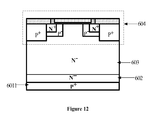
- the TI-IGBT includes: a first semiconductor substrate 601 , where a collector region 6011 and a short-circuit region 6012 disposed in parallel are formed in the first semiconductor substrate 601 ; a second semiconductor substrate 603 located above an upper surface of the first semiconductor substrate 601 ; and a first doped layer 602 located between the first semiconductor substrate 601 and the second semiconductor substrate 603 , and the first doped layer 602 covers at least the collector region 6011 in the first semiconductor substrate 601 , where the doping type of the first doped layer 602 is the same as that of the second semiconductor substrate 603 , and the doping concentration of the first doped layer 602 is lower than that of the second semiconductor substrate 603 .
- the TI-IGBT according to the embodiment of the present disclosure further includes a front structure 604 formed on a surface of the second semiconductor substrate 603 .
- the front structure includes: a gate structure formed on the surface of the second semiconductor substrate 603 , where the gate structure includes a gate dielectric layer formed on the surface of the second semiconductor substrate 603 and a gate electrode layer located on the surface of the gate dielectric layer; a base region formed on both sides of the gate structure and in the second semiconductor substrate 603 and a well region formed in the second semiconductor substrate 603 and located outside of the base region; and an emitter structure formed on both sides of the gate structure, where the emitter structure includes an emitter formed in the base region and an emitter electrode formed on the surfaces of the emitter region and the well region and electrically connected to the emitter region and the well region.
- the front structure of the second semiconductor substrate 603 is the same as that of the IGBT device in the conventional technology, which has been well known by those skilled in the art and thus is not described in detail in the embodiment of the present disclosure.
- the conductive ability of the semiconductor is closely related to the doping concentration thereof.
- the doping concentration of the first doped layer 602 is lower than that of the second semiconductor substrate 603 . Therefore, the conductive ability of the first doped layer 602 is lower than that of the second semiconductor substrate 603 , that is, the resistivity of the first doped layer 602 is higher than that of the second semiconductor substrate 603 .
- the voltage drop across a unit distance above the collector region 6011 is increased in the case that electrons gathered together above the collector region 6011 flow to the above of the short-circuit region 6012 , and thus the TI-IGBT enters into the IGBT mode at a smaller current, that is, the TI-IGBT enters into the conventional IGBT operation mode at a smaller current, to solve the current snap-back phenomenon occurred in the TI-IGBT in the conventional technology.
- the first semiconductor substrate 601 is completely covered by the first doped layer 602 in the TI-IGBT according to an embodiment of the present disclosure.
- a TI-IGBT in a TI-IGBT according to another embodiment of the present disclosure, only the collector region 6011 in the first semiconductor substrate 601 is covered by the first doped layer 602 , which ensures the release rate of the electrons above the short-circuit region 6012 and increases the turn-off speed of the TI-IGBT while avoiding the current snap-back phenomenon during the operation of the TI-IGBT. Moreover, since the first doped layer 602 does not cover the short-circuit region 6012 , the area of the first doped layer 602 is reduced, the number of the injected ions during the process of forming the first doped layer 602 is reduced and the fabrication cost of the TI-IGBT is reduced.
- the TI-IGBT further includes: a second doped layer 606 located between the second semiconductor substrate 603 and the short-circuit region 6012 in the first semiconductor substrate 601 .
- the doping type of the second doped layer 606 is the same as that of the second semiconductor substrate 603 , and the doping concentration of the second doped layer 606 is higher than that of the second semiconductor substrate 603 . Therefore, the electric field in the drift region during the operation of the TI-IGBT can be rapidly stopped, and the conduction voltage drop of the TI-IGBT can be further reduced.
- the first semiconductor substrate 601 may be completely covered by the first doped layer 602 , as shown in FIG. 6 , or only the collector region 6011 in the first semiconductor substrate 601 is covered by the first doped layer 602 , which is not limited in the present disclosure, as long as at least the collector region 6011 in the first semiconductor substrate 601 is covered by the first doped layer 602 .
- the first doped layer 602 preferably has a thickness of 1 ⁇ m to 10 ⁇ m, inclusive, and has a doping concentration of 10 12 ⁇ cm ⁇ 3 to 10 13 ⁇ cm ⁇ 3 , inclusive, which are not limited in the present disclosure and can be determined based on the structure and the application of the TI-IGBT.
- the TI-IGBT is a punch-through TI-IGBT
- the TI-IGBT according to the present disclosure further includes a buffer layer located between the first doped layer 602 and the second semiconductor substrate 603 .
- the doping type of the buffer layer is the same as that of the second semiconductor substrate 603 and the doping concentration of the buffer layer is higher than that of the second semiconductor substrate 603 .
- the TI-IGBT according to the embodiments of the present disclosure a first doped layer between the first semiconductor substrate and the second semiconductor substrate is added, with the doping type of the first doped layer being the same as that of the second semiconductor substrate and the doping concentration of the first doped layer being lower than that of the second semiconductor substrate, and thus the resistance above the collector region in the first semiconductor substrate is increased. Therefore, the TI-IGBT according to the present disclosure enters into the IGBT mode at a smaller current, thereby solving the current snap-back phenomenon during the operation of the TI-IGBT in the conventional technology.
- a formation method of a TI-IGBT is further provided according to the disclosure.
- the method includes the following.
- the first semiconductor substrate 601 may be an N-type silicon substrate or a P-type silicon substrate, which is not limited in the present disclosure.
- a first doped layer 602 is formed on an upper surface of the first semiconductor substrate 601 , as shown in FIG. 9 .
- the process for forming the first doped layer 602 is preferably an epitaxial process.
- a front structure is formed on an upper surface of the second semiconductor substrate 603 .
- the front structure includes: a gate structure formed on a surface of the second semiconductor substrate 603 , where the gate structure includes a gate dielectric layer formed on the surface of the second semiconductor substrate 603 and a gate electrode layer located on the surface of the gate dielectric layer; a base region formed on both sides of the gate structure and in the second semiconductor substrate 603 and a well region formed in the second semiconductor substrate 603 and located outside of the base region; and an emitter structure formed on both sides of the gate structure, where the emitter structure includes an emitter formed in the base region and an emitter electrode formed on the surfaces of the emitter region and the well region and electrically connected with the emitter region and the well region.
- the process for forming the front structure of the second semiconductor substrate 603 is well known by those skilled in the art and thus is not described in detail in the embodiment of the present disclosure.
- the lower surface of the first semiconductor substrate 601 is thinned on the back, as shown in FIG. 11 , and then a collector region 6011 and a short-circuit region 6012 disposed in parallel are formed in the first semiconductor substrate 601 .
- the first doped layer 602 covers at least the collector region 6011 in the first semiconductor substrate 601 , the doping type of the first doped layer 602 is the same as that of the second semiconductor substrate 603 , and the doping concentration of the first doped layer 602 is lower than that of the second semiconductor substrate 603 .
- a collector 605 is formed on the surfaces of the collector region 6011 and the short-circuit region 6012 .
- the collector 605 is electrically connected with the collector region 6011 and the short-circuit region 6012 .
- first photoresist on the lower surface of the first semiconductor substrate 601 , and forming a first window in the first photoresist, where the first window corresponds to a part of the first semiconductor substrate 601 where the collector region 6011 is to be formed;
- the process of thinning the lower surface of the first semiconductor substrate 601 on the back and then forming the collector region 6011 and the short-circuit region 6012 disposed in parallel in the first semiconductor substrate 601 includes:
- Another formation method of a TI-IGBT is further provided according to the disclosure.
- the method includes the following.
- the first semiconductor substrate 601 may be an N-type silicon substrate or a P-type silicon substrate, which is not limited in the present disclosure.
- a first doped layer 602 is formed on an upper surface of the first semiconductor substrate 601 .
- a second semiconductor substrate 603 is formed above the first semiconductor substrate 601 .
- the second semiconductor substrate 603 completely covers the first doped layer 602 and the first semiconductor substrate 601 .
- a front structure is formed on an upper surface of the second semiconductor substrate 603 .
- a lower surface of the first semiconductor substrate 601 is thinned on the back to expose the first doped layer 602 after the front structure of the second semiconductor substrate 603 is formed.
- a collector region and a short-circuit region disposed in parallel is formed in the first doped layer 602 .
- a collector 605 is formed on the surfaces of the collector region 6011 and the short-circuit region 6012 .
- the collector 605 is electrically connected with the collector region 6011 and the short-circuit region 6012 .
- the depths of the collector region and the short-circuit region should be strictly controlled in the case that the short-circuit region and the collector region are formed in the first doped layer 602 , so that the region of the first doped layer 602 where the collector region is not formed covers at least the collector region.
- the first doped layer 602 may completely cover the first semiconductor substrate 601 , or may cover only the collector region 6011 in the first semiconductor substrate 601 , which is not limited in the present disclosure, as long as the first doped layer 602 covers at least the collector region 6011 in the first semiconductor substrate 601 .
- the formation method of the TI-IGBT according to the embodiment of the present disclosure may further include forming a second doped layer 606 on an upper surface of the short-circuit region 6012 before forming the second semiconductor substrate 602 above the first semiconductor substrate 601 , as shown in FIG. 14 .
- the doping type of the second doped layer 606 is the same as that of the second semiconductor substrate 603 , and the doping concentration of the second doped layer 606 is higher than that of the second semiconductor substrate 603 . Therefore, the electric field in the drift region during the operation of the TI-IGBT can be rapidly stopped, and the conduction voltage drop of the TI-IGBT can be further reduced.
- the formation method further includes forming a buffer layer above the first doped layer 602 before forming the second semiconductor substrate 603 above the first semiconductor substrate 601 , as shown in FIG. 15 .
- the buffer layer completely covers first doped layer 602 and the first semiconductor substrate 601 .
- the doping type of the buffer layer is the same as that of the second semiconductor substrate 603 , and the doping concentration of the buffer layer is higher than that of the second semiconductor substrate 603 .
- a first doped layer between the first semiconductor substrate and the second semiconductor substrate is added, with the doping type of the first doped layer being the same as that of the second semiconductor substrate and the doping concentration of the first doped layer being lower than that of the second semiconductor substrate, and thus the resistance above the collector region in the first semiconductor substrate is increased. Therefore, the TI-IGBT according to the present disclosure enters into the IGBT mode at a smaller current, thereby solving the current snap-back phenomenon during the operation of the TI-IGBT in the conventional technology.
Landscapes
- Physics & Mathematics (AREA)
- Engineering & Computer Science (AREA)
- High Energy & Nuclear Physics (AREA)
- Condensed Matter Physics & Semiconductors (AREA)
- General Physics & Mathematics (AREA)
- Manufacturing & Machinery (AREA)
- Computer Hardware Design (AREA)
- Microelectronics & Electronic Packaging (AREA)
- Power Engineering (AREA)
- Electrodes Of Semiconductors (AREA)
- Health & Medical Sciences (AREA)
- Toxicology (AREA)
Abstract
Description
Claims (9)
Applications Claiming Priority (1)
| Application Number | Priority Date | Filing Date | Title |
|---|---|---|---|
| PCT/CN2012/086016 WO2014086015A1 (en) | 2012-12-06 | 2012-12-06 | Ti-igbt and formation method thereof |
Publications (2)
| Publication Number | Publication Date |
|---|---|
| US20150349102A1 US20150349102A1 (en) | 2015-12-03 |
| US9461116B2 true US9461116B2 (en) | 2016-10-04 |
Family
ID=50882774
Family Applications (1)
| Application Number | Title | Priority Date | Filing Date |
|---|---|---|---|
| US14/649,553 Expired - Fee Related US9461116B2 (en) | 2012-12-06 | 2012-12-06 | Method of formation of a TI-IGBT |
Country Status (2)
| Country | Link |
|---|---|
| US (1) | US9461116B2 (en) |
| WO (1) | WO2014086015A1 (en) |
Families Citing this family (3)
| Publication number | Priority date | Publication date | Assignee | Title |
|---|---|---|---|---|
| CN104022033B (en) * | 2014-06-18 | 2016-08-24 | 江苏中科君芯科技有限公司 | A kind of processing method of TI-IGBT chip back structure |
| CN104157683B (en) * | 2014-08-21 | 2018-03-09 | 株洲南车时代电气股份有限公司 | Igbt chip and preparation method thereof |
| CN105762174A (en) * | 2016-05-13 | 2016-07-13 | 上海芯石微电子有限公司 | Fast recovery diode material slice structure containing cathode auxiliary part and manufacturing method thereof |
Citations (9)
| Publication number | Priority date | Publication date | Assignee | Title |
|---|---|---|---|---|
| US5352910A (en) * | 1992-04-07 | 1994-10-04 | Tokyo Denki Seizo Kabushiki Kaisha | Semiconductor device with a buffer structure |
| US20050017290A1 (en) * | 2003-07-24 | 2005-01-27 | Mitsubishi Denki Kabushiki Kaisha | Insulated gate bipolar transistor with built-in freewheeling diode |
| CN101123270A (en) | 2006-08-09 | 2008-02-13 | 三垦电气株式会社 | Semiconductor device |
| CN101499422A (en) | 2008-12-12 | 2009-08-05 | 北京工业大学 | Production method for inner transparent collecting electrode IGBT with polysilicon as service life control layer |
| US20100230716A1 (en) * | 2009-03-13 | 2010-09-16 | Kabushiki Kaisha Toshiba | Semiconductor device |
| CN101887913A (en) | 2010-06-04 | 2010-11-17 | 无锡新洁能功率半导体有限公司 | IGBT with improved collector structure |
| US20100301386A1 (en) * | 2009-06-02 | 2010-12-02 | Wei-Chieh Lin | Integrated structure of igbt and diode and method of forming the same |
| US20110180902A1 (en) | 2010-01-27 | 2011-07-28 | Renesas Electronics Corporation | Reverse conducting igbt |
| US20120068220A1 (en) * | 2010-09-21 | 2012-03-22 | Kabushiki Kaisha Toshiba | Reverse conducting-insulated gate bipolar transistor |
-
2012
- 2012-12-06 WO PCT/CN2012/086016 patent/WO2014086015A1/en not_active Ceased
- 2012-12-06 US US14/649,553 patent/US9461116B2/en not_active Expired - Fee Related
Patent Citations (9)
| Publication number | Priority date | Publication date | Assignee | Title |
|---|---|---|---|---|
| US5352910A (en) * | 1992-04-07 | 1994-10-04 | Tokyo Denki Seizo Kabushiki Kaisha | Semiconductor device with a buffer structure |
| US20050017290A1 (en) * | 2003-07-24 | 2005-01-27 | Mitsubishi Denki Kabushiki Kaisha | Insulated gate bipolar transistor with built-in freewheeling diode |
| CN101123270A (en) | 2006-08-09 | 2008-02-13 | 三垦电气株式会社 | Semiconductor device |
| CN101499422A (en) | 2008-12-12 | 2009-08-05 | 北京工业大学 | Production method for inner transparent collecting electrode IGBT with polysilicon as service life control layer |
| US20100230716A1 (en) * | 2009-03-13 | 2010-09-16 | Kabushiki Kaisha Toshiba | Semiconductor device |
| US20100301386A1 (en) * | 2009-06-02 | 2010-12-02 | Wei-Chieh Lin | Integrated structure of igbt and diode and method of forming the same |
| US20110180902A1 (en) | 2010-01-27 | 2011-07-28 | Renesas Electronics Corporation | Reverse conducting igbt |
| CN101887913A (en) | 2010-06-04 | 2010-11-17 | 无锡新洁能功率半导体有限公司 | IGBT with improved collector structure |
| US20120068220A1 (en) * | 2010-09-21 | 2012-03-22 | Kabushiki Kaisha Toshiba | Reverse conducting-insulated gate bipolar transistor |
Non-Patent Citations (2)
| Title |
|---|
| International Search Report from PCT/CN2012/086016 (Sep. 12, 2013). |
| Written Opinion from PCT/CN2012/086016 (Sep. 12, 2013). |
Also Published As
| Publication number | Publication date |
|---|---|
| WO2014086015A1 (en) | 2014-06-12 |
| US20150349102A1 (en) | 2015-12-03 |
Similar Documents
| Publication | Publication Date | Title |
|---|---|---|
| US9799648B2 (en) | Semiconductor device | |
| US8809903B2 (en) | Semiconductor device and power conversion apparatus using the same | |
| CN105742346B (en) | Double division trench gate charge storage type RC-IGBT and its manufacturing method | |
| CN107180865B (en) | A Low Noise Low Loss Insulated Gate Bipolar Transistor | |
| CN104347689B (en) | Double Trench-Gated IGBT Structure | |
| US11081574B2 (en) | IGBT power device | |
| CN106997899B (en) | A kind of IGBT device and preparation method thereof | |
| US10340373B2 (en) | Reverse conducting IGBT | |
| CN104576741B (en) | A kind of power semiconductor structure and forming method thereof | |
| CN103383957B (en) | A kind of inverse conductivity type IGBT device | |
| CN109728084B (en) | A planar gate IGBT device with deep trench electric field shielding structure | |
| WO2023071237A1 (en) | Insulated gate bipolar transistor and manufacturing method therefor, and electronic device | |
| CN110400840A (en) | An RC-LIGBT Device that Suppresses Voltage Bending Phenomenon | |
| CN107634094B (en) | Insulated gate bipolar transistor structure and manufacturing method thereof | |
| CN111834449A (en) | A fast turn-off RC-IGBT device with backside dual MOS structure | |
| CN110504305B (en) | SOI-LIGBT device with self-biased pmos clamp carrier storage layer | |
| CN105489644B (en) | IGBT device and preparation method thereof | |
| CN103855155A (en) | A three-mode integrated insulated gate bipolar transistor and its forming method | |
| US11276686B2 (en) | Semiconductor device | |
| US9461116B2 (en) | Method of formation of a TI-IGBT | |
| CN110610986B (en) | RC-IGBT device integrating transverse freewheeling diode by using junction terminal | |
| KR102585094B1 (en) | Separated Buffer Super Junction IGBT | |
| CN103915489B (en) | Insulated gate bipolar transistor | |
| US20170170310A1 (en) | Semiconductor device and manufacturing method of the semiconductor device | |
| US20150144990A1 (en) | Power semiconductor device and method of manufacturing the same |
Legal Events
| Date | Code | Title | Description |
|---|---|---|---|
| AS | Assignment |
Owner name: INSTITUTE OF MICROELECTRONICS, CHINESE ACADEMY OF Free format text: ASSIGNMENT OF ASSIGNORS INTEREST;ASSIGNORS:ZHU, YANGJUN;ZHANG, WENLIANG;LU, SHUOJIN;AND OTHERS;REEL/FRAME:035782/0487 Effective date: 20150516 Owner name: JIANGSU CAS-IGBT TECHNOLOGY CO., LTD., CHINA Free format text: ASSIGNMENT OF ASSIGNORS INTEREST;ASSIGNORS:ZHU, YANGJUN;ZHANG, WENLIANG;LU, SHUOJIN;AND OTHERS;REEL/FRAME:035782/0487 Effective date: 20150516 Owner name: SHANGHAI LIANXING ELECTRONICS CO., LTD., CHINA Free format text: ASSIGNMENT OF ASSIGNORS INTEREST;ASSIGNORS:ZHU, YANGJUN;ZHANG, WENLIANG;LU, SHUOJIN;AND OTHERS;REEL/FRAME:035782/0487 Effective date: 20150516 |
|
| STCF | Information on status: patent grant |
Free format text: PATENTED CASE |
|
| MAFP | Maintenance fee payment |
Free format text: PAYMENT OF MAINTENANCE FEE, 4TH YEAR, LARGE ENTITY (ORIGINAL EVENT CODE: M1551); ENTITY STATUS OF PATENT OWNER: LARGE ENTITY Year of fee payment: 4 |
|
| FEPP | Fee payment procedure |
Free format text: MAINTENANCE FEE REMINDER MAILED (ORIGINAL EVENT CODE: REM.); ENTITY STATUS OF PATENT OWNER: LARGE ENTITY |
|
| LAPS | Lapse for failure to pay maintenance fees |
Free format text: PATENT EXPIRED FOR FAILURE TO PAY MAINTENANCE FEES (ORIGINAL EVENT CODE: EXP.); ENTITY STATUS OF PATENT OWNER: LARGE ENTITY |
|
| STCH | Information on status: patent discontinuation |
Free format text: PATENT EXPIRED DUE TO NONPAYMENT OF MAINTENANCE FEES UNDER 37 CFR 1.362 |
|
| FP | Lapsed due to failure to pay maintenance fee |
Effective date: 20241004 |