US9460771B2 - Two-transistor thyristor SRAM circuit and methods of operation - Google Patents
Two-transistor thyristor SRAM circuit and methods of operation Download PDFInfo
- Publication number
- US9460771B2 US9460771B2 US14/607,023 US201514607023A US9460771B2 US 9460771 B2 US9460771 B2 US 9460771B2 US 201514607023 A US201514607023 A US 201514607023A US 9460771 B2 US9460771 B2 US 9460771B2
- Authority
- US
- United States
- Prior art keywords
- voltage
- thyristor
- transistor
- sram cell
- cell
- Prior art date
- Legal status (The legal status is an assumption and is not a legal conclusion. Google has not performed a legal analysis and makes no representation as to the accuracy of the status listed.)
- Active
Links
- 238000000034 method Methods 0.000 title claims abstract description 71
- 230000015654 memory Effects 0.000 claims abstract description 241
- 230000008569 process Effects 0.000 abstract description 51
- 238000005516 engineering process Methods 0.000 abstract description 29
- 239000000758 substrate Substances 0.000 abstract description 29
- 239000004065 semiconductor Substances 0.000 abstract description 24
- 238000002955 isolation Methods 0.000 abstract description 22
- 238000004519 manufacturing process Methods 0.000 abstract description 16
- 239000010410 layer Substances 0.000 description 28
- 230000000295 complement effect Effects 0.000 description 26
- 238000010586 diagram Methods 0.000 description 22
- 229910052751 metal Inorganic materials 0.000 description 18
- 239000002184 metal Substances 0.000 description 18
- VYPSYNLAJGMNEJ-UHFFFAOYSA-N Silicium dioxide Chemical compound O=[Si]=O VYPSYNLAJGMNEJ-UHFFFAOYSA-N 0.000 description 16
- 230000002829 reductive effect Effects 0.000 description 15
- 239000007943 implant Substances 0.000 description 12
- 238000013459 approach Methods 0.000 description 10
- 239000002019 doping agent Substances 0.000 description 10
- 230000008901 benefit Effects 0.000 description 9
- 239000003990 capacitor Substances 0.000 description 9
- 230000000873 masking effect Effects 0.000 description 8
- 229920002120 photoresistant polymer Polymers 0.000 description 8
- 230000015572 biosynthetic process Effects 0.000 description 7
- 238000013461 design Methods 0.000 description 7
- 230000005669 field effect Effects 0.000 description 7
- 235000012239 silicon dioxide Nutrition 0.000 description 7
- 239000000377 silicon dioxide Substances 0.000 description 7
- HQVNEWCFYHHQES-UHFFFAOYSA-N silicon nitride Chemical compound N12[Si]34N5[Si]62N3[Si]51N64 HQVNEWCFYHHQES-UHFFFAOYSA-N 0.000 description 7
- XUIMIQQOPSSXEZ-UHFFFAOYSA-N Silicon Chemical compound [Si] XUIMIQQOPSSXEZ-UHFFFAOYSA-N 0.000 description 6
- 238000003491 array Methods 0.000 description 6
- 229910052710 silicon Inorganic materials 0.000 description 6
- 239000010703 silicon Substances 0.000 description 6
- 229910052581 Si3N4 Inorganic materials 0.000 description 5
- 230000008878 coupling Effects 0.000 description 5
- 238000010168 coupling process Methods 0.000 description 5
- 238000005859 coupling reaction Methods 0.000 description 5
- 238000006880 cross-coupling reaction Methods 0.000 description 5
- 238000002513 implantation Methods 0.000 description 5
- 239000012535 impurity Substances 0.000 description 5
- 238000012545 processing Methods 0.000 description 5
- 230000008859 change Effects 0.000 description 4
- 230000007423 decrease Effects 0.000 description 4
- 230000006870 function Effects 0.000 description 4
- 238000011161 development Methods 0.000 description 3
- 229910044991 metal oxide Inorganic materials 0.000 description 3
- 150000004706 metal oxides Chemical class 0.000 description 3
- 238000012986 modification Methods 0.000 description 3
- 230000004048 modification Effects 0.000 description 3
- 229910021420 polycrystalline silicon Inorganic materials 0.000 description 3
- 230000007704 transition Effects 0.000 description 3
- 230000001668 ameliorated effect Effects 0.000 description 2
- 239000000969 carrier Substances 0.000 description 2
- 230000001419 dependent effect Effects 0.000 description 2
- 230000000694 effects Effects 0.000 description 2
- 238000007667 floating Methods 0.000 description 2
- 239000011810 insulating material Substances 0.000 description 2
- 230000010354 integration Effects 0.000 description 2
- 238000012423 maintenance Methods 0.000 description 2
- 150000004767 nitrides Chemical class 0.000 description 2
- 230000002441 reversible effect Effects 0.000 description 2
- 230000000630 rising effect Effects 0.000 description 2
- 238000000926 separation method Methods 0.000 description 2
- 230000003213 activating effect Effects 0.000 description 1
- 229910052782 aluminium Inorganic materials 0.000 description 1
- XAGFODPZIPBFFR-UHFFFAOYSA-N aluminium Chemical compound [Al] XAGFODPZIPBFFR-UHFFFAOYSA-N 0.000 description 1
- 239000004020 conductor Substances 0.000 description 1
- 238000010276 construction Methods 0.000 description 1
- 230000003247 decreasing effect Effects 0.000 description 1
- 230000001976 improved effect Effects 0.000 description 1
- 230000006872 improvement Effects 0.000 description 1
- 238000005468 ion implantation Methods 0.000 description 1
- 230000000670 limiting effect Effects 0.000 description 1
- 239000000463 material Substances 0.000 description 1
- 230000006386 memory function Effects 0.000 description 1
- 230000003647 oxidation Effects 0.000 description 1
- 238000007254 oxidation reaction Methods 0.000 description 1
- 238000012856 packing Methods 0.000 description 1
- 230000036961 partial effect Effects 0.000 description 1
- 229920005591 polysilicon Polymers 0.000 description 1
- 238000011165 process development Methods 0.000 description 1
- 238000011112 process operation Methods 0.000 description 1
- 230000002035 prolonged effect Effects 0.000 description 1
- 238000005215 recombination Methods 0.000 description 1
- 230000006798 recombination Effects 0.000 description 1
- 238000011160 research Methods 0.000 description 1
- 238000012827 research and development Methods 0.000 description 1
- 230000004044 response Effects 0.000 description 1
- 229910052814 silicon oxide Inorganic materials 0.000 description 1
- 239000002356 single layer Substances 0.000 description 1
- 125000006850 spacer group Chemical group 0.000 description 1
- 230000003068 static effect Effects 0.000 description 1
- 238000003860 storage Methods 0.000 description 1
- 230000008093 supporting effect Effects 0.000 description 1
- 238000013519 translation Methods 0.000 description 1
Images


Classifications
-
- G—PHYSICS
- G11—INFORMATION STORAGE
- G11C—STATIC STORES
- G11C11/00—Digital stores characterised by the use of particular electric or magnetic storage elements; Storage elements therefor
- G11C11/21—Digital stores characterised by the use of particular electric or magnetic storage elements; Storage elements therefor using electric elements
- G11C11/34—Digital stores characterised by the use of particular electric or magnetic storage elements; Storage elements therefor using electric elements using semiconductor devices
- G11C11/39—Digital stores characterised by the use of particular electric or magnetic storage elements; Storage elements therefor using electric elements using semiconductor devices using thyristors or the avalanche or negative resistance type, e.g. PNPN, SCR, SCS, UJT
-
- G—PHYSICS
- G11—INFORMATION STORAGE
- G11C—STATIC STORES
- G11C11/00—Digital stores characterised by the use of particular electric or magnetic storage elements; Storage elements therefor
- G11C11/21—Digital stores characterised by the use of particular electric or magnetic storage elements; Storage elements therefor using electric elements
- G11C11/34—Digital stores characterised by the use of particular electric or magnetic storage elements; Storage elements therefor using electric elements using semiconductor devices
- G11C11/40—Digital stores characterised by the use of particular electric or magnetic storage elements; Storage elements therefor using electric elements using semiconductor devices using transistors
- G11C11/41—Digital stores characterised by the use of particular electric or magnetic storage elements; Storage elements therefor using electric elements using semiconductor devices using transistors forming static cells with positive feedback, i.e. cells not needing refreshing or charge regeneration, e.g. bistable multivibrator or Schmitt trigger
- G11C11/413—Auxiliary circuits, e.g. for addressing, decoding, driving, writing, sensing, timing or power reduction
- G11C11/417—Auxiliary circuits, e.g. for addressing, decoding, driving, writing, sensing, timing or power reduction for memory cells of the field-effect type
- G11C11/418—Address circuits
-
- G—PHYSICS
- G11—INFORMATION STORAGE
- G11C—STATIC STORES
- G11C11/00—Digital stores characterised by the use of particular electric or magnetic storage elements; Storage elements therefor
- G11C11/21—Digital stores characterised by the use of particular electric or magnetic storage elements; Storage elements therefor using electric elements
- G11C11/34—Digital stores characterised by the use of particular electric or magnetic storage elements; Storage elements therefor using electric elements using semiconductor devices
- G11C11/40—Digital stores characterised by the use of particular electric or magnetic storage elements; Storage elements therefor using electric elements using semiconductor devices using transistors
- G11C11/41—Digital stores characterised by the use of particular electric or magnetic storage elements; Storage elements therefor using electric elements using semiconductor devices using transistors forming static cells with positive feedback, i.e. cells not needing refreshing or charge regeneration, e.g. bistable multivibrator or Schmitt trigger
- G11C11/413—Auxiliary circuits, e.g. for addressing, decoding, driving, writing, sensing, timing or power reduction
- G11C11/417—Auxiliary circuits, e.g. for addressing, decoding, driving, writing, sensing, timing or power reduction for memory cells of the field-effect type
- G11C11/419—Read-write [R-W] circuits
-
- H—ELECTRICITY
- H01—ELECTRIC ELEMENTS
- H01L—SEMICONDUCTOR DEVICES NOT COVERED BY CLASS H10
- H01L21/00—Processes or apparatus adapted for the manufacture or treatment of semiconductor or solid state devices or of parts thereof
- H01L21/70—Manufacture or treatment of devices consisting of a plurality of solid state components formed in or on a common substrate or of parts thereof; Manufacture of integrated circuit devices or of parts thereof
- H01L21/77—Manufacture or treatment of devices consisting of a plurality of solid state components or integrated circuits formed in, or on, a common substrate
- H01L21/78—Manufacture or treatment of devices consisting of a plurality of solid state components or integrated circuits formed in, or on, a common substrate with subsequent division of the substrate into plural individual devices
- H01L21/82—Manufacture or treatment of devices consisting of a plurality of solid state components or integrated circuits formed in, or on, a common substrate with subsequent division of the substrate into plural individual devices to produce devices, e.g. integrated circuits, each consisting of a plurality of components
- H01L21/822—Manufacture or treatment of devices consisting of a plurality of solid state components or integrated circuits formed in, or on, a common substrate with subsequent division of the substrate into plural individual devices to produce devices, e.g. integrated circuits, each consisting of a plurality of components the substrate being a semiconductor, using silicon technology
- H01L21/8248—Combination of bipolar and field-effect technology
- H01L21/8249—Bipolar and MOS technology
-
- H—ELECTRICITY
- H01—ELECTRIC ELEMENTS
- H01L—SEMICONDUCTOR DEVICES NOT COVERED BY CLASS H10
- H01L27/00—Devices consisting of a plurality of semiconductor or other solid-state components formed in or on a common substrate
- H01L27/02—Devices consisting of a plurality of semiconductor or other solid-state components formed in or on a common substrate including semiconductor components specially adapted for rectifying, oscillating, amplifying or switching and having potential barriers; including integrated passive circuit elements having potential barriers
- H01L27/04—Devices consisting of a plurality of semiconductor or other solid-state components formed in or on a common substrate including semiconductor components specially adapted for rectifying, oscillating, amplifying or switching and having potential barriers; including integrated passive circuit elements having potential barriers the substrate being a semiconductor body
- H01L27/06—Devices consisting of a plurality of semiconductor or other solid-state components formed in or on a common substrate including semiconductor components specially adapted for rectifying, oscillating, amplifying or switching and having potential barriers; including integrated passive circuit elements having potential barriers the substrate being a semiconductor body including a plurality of individual components in a non-repetitive configuration
- H01L27/0611—Devices consisting of a plurality of semiconductor or other solid-state components formed in or on a common substrate including semiconductor components specially adapted for rectifying, oscillating, amplifying or switching and having potential barriers; including integrated passive circuit elements having potential barriers the substrate being a semiconductor body including a plurality of individual components in a non-repetitive configuration integrated circuits having a two-dimensional layout of components without a common active region
- H01L27/0617—Devices consisting of a plurality of semiconductor or other solid-state components formed in or on a common substrate including semiconductor components specially adapted for rectifying, oscillating, amplifying or switching and having potential barriers; including integrated passive circuit elements having potential barriers the substrate being a semiconductor body including a plurality of individual components in a non-repetitive configuration integrated circuits having a two-dimensional layout of components without a common active region comprising components of the field-effect type
- H01L27/0623—Devices consisting of a plurality of semiconductor or other solid-state components formed in or on a common substrate including semiconductor components specially adapted for rectifying, oscillating, amplifying or switching and having potential barriers; including integrated passive circuit elements having potential barriers the substrate being a semiconductor body including a plurality of individual components in a non-repetitive configuration integrated circuits having a two-dimensional layout of components without a common active region comprising components of the field-effect type in combination with bipolar transistors
-
- H01L27/11—
-
- H—ELECTRICITY
- H10—SEMICONDUCTOR DEVICES; ELECTRIC SOLID-STATE DEVICES NOT OTHERWISE PROVIDED FOR
- H10B—ELECTRONIC MEMORY DEVICES
- H10B10/00—Static random access memory [SRAM] devices
- H10B10/10—SRAM devices comprising bipolar components
-
- H—ELECTRICITY
- H10—SEMICONDUCTOR DEVICES; ELECTRIC SOLID-STATE DEVICES NOT OTHERWISE PROVIDED FOR
- H10B—ELECTRONIC MEMORY DEVICES
- H10B10/00—Static random access memory [SRAM] devices
- H10B10/12—Static random access memory [SRAM] devices comprising a MOSFET load element
-
- G—PHYSICS
- G11—INFORMATION STORAGE
- G11C—STATIC STORES
- G11C11/00—Digital stores characterised by the use of particular electric or magnetic storage elements; Storage elements therefor
- G11C11/21—Digital stores characterised by the use of particular electric or magnetic storage elements; Storage elements therefor using electric elements
- G11C11/34—Digital stores characterised by the use of particular electric or magnetic storage elements; Storage elements therefor using electric elements using semiconductor devices
- G11C11/40—Digital stores characterised by the use of particular electric or magnetic storage elements; Storage elements therefor using electric elements using semiconductor devices using transistors
- G11C11/41—Digital stores characterised by the use of particular electric or magnetic storage elements; Storage elements therefor using electric elements using semiconductor devices using transistors forming static cells with positive feedback, i.e. cells not needing refreshing or charge regeneration, e.g. bistable multivibrator or Schmitt trigger
- G11C11/411—Digital stores characterised by the use of particular electric or magnetic storage elements; Storage elements therefor using electric elements using semiconductor devices using transistors forming static cells with positive feedback, i.e. cells not needing refreshing or charge regeneration, e.g. bistable multivibrator or Schmitt trigger using bipolar transistors only
- G11C11/4113—Digital stores characterised by the use of particular electric or magnetic storage elements; Storage elements therefor using electric elements using semiconductor devices using transistors forming static cells with positive feedback, i.e. cells not needing refreshing or charge regeneration, e.g. bistable multivibrator or Schmitt trigger using bipolar transistors only with at least one cell access to base or collector of at least one of said transistors, e.g. via access diodes, access transistors
-
- G—PHYSICS
- G11—INFORMATION STORAGE
- G11C—STATIC STORES
- G11C11/00—Digital stores characterised by the use of particular electric or magnetic storage elements; Storage elements therefor
- G11C11/21—Digital stores characterised by the use of particular electric or magnetic storage elements; Storage elements therefor using electric elements
- G11C11/34—Digital stores characterised by the use of particular electric or magnetic storage elements; Storage elements therefor using electric elements using semiconductor devices
- G11C11/40—Digital stores characterised by the use of particular electric or magnetic storage elements; Storage elements therefor using electric elements using semiconductor devices using transistors
- G11C11/41—Digital stores characterised by the use of particular electric or magnetic storage elements; Storage elements therefor using electric elements using semiconductor devices using transistors forming static cells with positive feedback, i.e. cells not needing refreshing or charge regeneration, e.g. bistable multivibrator or Schmitt trigger
- G11C11/413—Auxiliary circuits, e.g. for addressing, decoding, driving, writing, sensing, timing or power reduction
- G11C11/414—Auxiliary circuits, e.g. for addressing, decoding, driving, writing, sensing, timing or power reduction for memory cells of the bipolar type
- G11C11/416—Read-write [R-W] circuits
-
- G—PHYSICS
- G11—INFORMATION STORAGE
- G11C—STATIC STORES
- G11C5/00—Details of stores covered by group G11C11/00
- G11C5/14—Power supply arrangements, e.g. power down, chip selection or deselection, layout of wirings or power grids, or multiple supply levels
-
- H—ELECTRICITY
- H01—ELECTRIC ELEMENTS
- H01L—SEMICONDUCTOR DEVICES NOT COVERED BY CLASS H10
- H01L27/00—Devices consisting of a plurality of semiconductor or other solid-state components formed in or on a common substrate
- H01L27/02—Devices consisting of a plurality of semiconductor or other solid-state components formed in or on a common substrate including semiconductor components specially adapted for rectifying, oscillating, amplifying or switching and having potential barriers; including integrated passive circuit elements having potential barriers
- H01L27/04—Devices consisting of a plurality of semiconductor or other solid-state components formed in or on a common substrate including semiconductor components specially adapted for rectifying, oscillating, amplifying or switching and having potential barriers; including integrated passive circuit elements having potential barriers the substrate being a semiconductor body
- H01L27/08—Devices consisting of a plurality of semiconductor or other solid-state components formed in or on a common substrate including semiconductor components specially adapted for rectifying, oscillating, amplifying or switching and having potential barriers; including integrated passive circuit elements having potential barriers the substrate being a semiconductor body including only semiconductor components of a single kind
- H01L27/082—Devices consisting of a plurality of semiconductor or other solid-state components formed in or on a common substrate including semiconductor components specially adapted for rectifying, oscillating, amplifying or switching and having potential barriers; including integrated passive circuit elements having potential barriers the substrate being a semiconductor body including only semiconductor components of a single kind including bipolar components only
- H01L27/0821—Combination of lateral and vertical transistors only
-
- H—ELECTRICITY
- H01—ELECTRIC ELEMENTS
- H01L—SEMICONDUCTOR DEVICES NOT COVERED BY CLASS H10
- H01L27/00—Devices consisting of a plurality of semiconductor or other solid-state components formed in or on a common substrate
- H01L27/02—Devices consisting of a plurality of semiconductor or other solid-state components formed in or on a common substrate including semiconductor components specially adapted for rectifying, oscillating, amplifying or switching and having potential barriers; including integrated passive circuit elements having potential barriers
- H01L27/04—Devices consisting of a plurality of semiconductor or other solid-state components formed in or on a common substrate including semiconductor components specially adapted for rectifying, oscillating, amplifying or switching and having potential barriers; including integrated passive circuit elements having potential barriers the substrate being a semiconductor body
- H01L27/08—Devices consisting of a plurality of semiconductor or other solid-state components formed in or on a common substrate including semiconductor components specially adapted for rectifying, oscillating, amplifying or switching and having potential barriers; including integrated passive circuit elements having potential barriers the substrate being a semiconductor body including only semiconductor components of a single kind
- H01L27/082—Devices consisting of a plurality of semiconductor or other solid-state components formed in or on a common substrate including semiconductor components specially adapted for rectifying, oscillating, amplifying or switching and having potential barriers; including integrated passive circuit elements having potential barriers the substrate being a semiconductor body including only semiconductor components of a single kind including bipolar components only
- H01L27/0823—Devices consisting of a plurality of semiconductor or other solid-state components formed in or on a common substrate including semiconductor components specially adapted for rectifying, oscillating, amplifying or switching and having potential barriers; including integrated passive circuit elements having potential barriers the substrate being a semiconductor body including only semiconductor components of a single kind including bipolar components only including vertical bipolar transistors only
- H01L27/0826—Combination of vertical complementary transistors
-
- H—ELECTRICITY
- H01—ELECTRIC ELEMENTS
- H01L—SEMICONDUCTOR DEVICES NOT COVERED BY CLASS H10
- H01L27/00—Devices consisting of a plurality of semiconductor or other solid-state components formed in or on a common substrate
- H01L27/02—Devices consisting of a plurality of semiconductor or other solid-state components formed in or on a common substrate including semiconductor components specially adapted for rectifying, oscillating, amplifying or switching and having potential barriers; including integrated passive circuit elements having potential barriers
- H01L27/04—Devices consisting of a plurality of semiconductor or other solid-state components formed in or on a common substrate including semiconductor components specially adapted for rectifying, oscillating, amplifying or switching and having potential barriers; including integrated passive circuit elements having potential barriers the substrate being a semiconductor body
- H01L27/10—Devices consisting of a plurality of semiconductor or other solid-state components formed in or on a common substrate including semiconductor components specially adapted for rectifying, oscillating, amplifying or switching and having potential barriers; including integrated passive circuit elements having potential barriers the substrate being a semiconductor body including a plurality of individual components in a repetitive configuration
- H01L27/102—Devices consisting of a plurality of semiconductor or other solid-state components formed in or on a common substrate including semiconductor components specially adapted for rectifying, oscillating, amplifying or switching and having potential barriers; including integrated passive circuit elements having potential barriers the substrate being a semiconductor body including a plurality of individual components in a repetitive configuration including bipolar components
- H01L27/1027—Thyristors
-
- H—ELECTRICITY
- H10—SEMICONDUCTOR DEVICES; ELECTRIC SOLID-STATE DEVICES NOT OTHERWISE PROVIDED FOR
- H10B—ELECTRONIC MEMORY DEVICES
- H10B10/00—Static random access memory [SRAM] devices
Definitions
- This invention is related to integrated circuit devices having memory functions and, in particular, to static random access memory (SRAM) devices.
- SRAM static random access memory
- Bipolar technology for semiconductor memory has been investigated over the years. But this research has typically focused upon the individual memory cell and has stopped at the conclusion that the memory cell could be part of an array. Further research and development of a bipolar memory cell array has been hampered by the longstanding belief that the CMOS memory cells occupied less space and consumed less power than any bipolar memory cell and that any bipolar memory cell array would necessarily be inferior to a CMOS array. Progress in recent years has relied upon relentless scaling in semiconductor processing technology, thus shrinking memory cell dimensions for greater circuit densities and higher operational speeds.
- CMOS complementary metal-oxide-semiconductor
- SRAM bistable latching circuitry
- Two cross-coupled inverters each of which includes an active transistor and a complementary load transistor, and two select transistors, form the six-transistor CMOS SRAM cell which has been used for decades.
- Many integrated circuits in use today require a combination of CMOS logic circuits and on-chip high performance memories. Modern high performance processors and System-on-Chip (SoC) applications demands more on-chip memory to meet the performance and throughput requirements.
- one integrated circuit can include 32 megabytes of CMOS SRAM as a cache memory on the chip.
- V DD 0.9 volts
- leakage current 25 nanoamperes per memory cell
- such a circuit consumes 7 amperes just from the memory array, without considering the power consumption of the logic portion of the chip.
- the stability and power consumption of the memory cells have become one of the limiting factors in process cost and circuit complexity, making the designers of such chips reluctant to use the latest process technology.
- CMOS SRAM in such devices typically has an access time on the order of 200 picoseconds with a standard deviation of 30 picoseconds. Thus to obtain 6 ⁇ sigma reliability an additional allowance of 6 ⁇ 30 picoseconds is necessary, resulting in a requirement to allow 380 picoseconds for access to the memory cells.
- the use of faster bipolar technology in such devices is typically limited to driver circuits in the SRAM memory, and even when used there, a more complicated bipolar CMOS (BiCMOS) fabrication process is used, requiring additional thermal cycles and making the fabrication of the MOS devices more difficult and expensive.
- BiCMOS bipolar CMOS
- the present invention provides for an SRAM memory cell that is based upon a thyristor, one form of bipolar technology and often represented by two coupled bipolar transistors.
- the memory cell is highly adaptable with many variations and the resulting SRAM integrated circuit can be designed for high-speed operation, or for lower speed operation if less power is required, or even for higher integration if a tightly packed SRAM integrated circuit is required.
- the SRAM memory cell can be manufactured with conventional CMOS technologies to avoid the development costs of a new technology.
- each memory cell comprising a pair of cross-coupled thyristors; a pair of bipolar transistors, each bipolar transistor respectively having a base region connected to a word line, an emitter region connected to one of the thyristors and a collector region connected to one of the pair of complementary bit lines; and an electrically isolated tub holding the pair of cross-coupled thyristors, and the tub in the substrate and electrically biased so that voltages on the word line within the logic circuit voltage range turn the pair of bipolar transistors on and off to connect and disconnect the cross-coupled thyristors to the pair of complementary bit lines.
- a process for forming a pair of cross-coupled bipolar transistors to form the thyristors described above includes steps of forming an annular region of insulating material extending into the upper surface of a first conductivity type semiconductor substrate to define a tub in the substrate, and introducing opposite conductivity type dopant to form a buried layer at the bottom of the tub. First conductivity type dopant is then implanted into the tub to form a deep well region extending to the buried layer. Next opposite conductivity type dopant is implanted to form a shallow well.
- the resulting semiconductor structure provides a cross-coupled pair of first type and opposite type bipolar transistors in which the annular insulating region extends into the substrate to surround a first portion of the upper surface of the substrate with a buried layer of opposite conductivity type to the first conductivity type disposed in the substrate beneath the first portion of the upper surface.
- a connecting region of first conductivity type extends to the buried layer to provide an electrical connection to it.
- a shallow well region of opposite conductivity type extends from the upper surface into the substrate over a second portion of the upper surface smaller than the first portion.
- a base contact of first conductivity type extends into the tub outside the first portion of the upper surface.
- a dummy field effect transistor gate is provided over the shallow well region to enable self-aligned implanting of emitter and collector regions adjacent the gate.
- the buried layer provides an emitter of the first type bipolar transistor and is coupled to a first voltage supply.
- the first conductivity type region adjacent one side of the gate provides an emitter region for the opposite type bipolar transistor and is coupled to a second voltage supply.
- the part of the tub beneath the shallow well provides a base for the first type bipolar transistor and a collector for the opposite type bipolar transistor, and the shallow well provides a base for the opposite type bipolar transistor and a collector for the first type bipolar transistor.
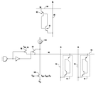
- FIG. 1A is a circuit diagram of a thyristor
- FIG. 1B shows a circuit diagram of cross-coupled thyristors that form a memory cell.
- FIG. 2 illustrates an array of SRAM memory cells.
- FIG. 3A is a circuit diagram of a cross-coupled thyristor memory cell with bipolar select transistors; and FIG. 3B is circuit diagram of a memory cell with MOS select transistors.
- FIG. 4A is a circuit diagram of a cross-coupled memory cell without select transistors
- FIG. 4B illustrates a cross point array of FIG. 4A memory cells with voltages on bit and word lines for a Write operation
- FIG. 4C illustrates the cross point array of FIG. 4A memory cells with voltages on bit and word lines for a Read operation
- FIG. 4D shows a low-power Write operation for a cross-coupled thyristor memory cell array connected to complementary bit lines and word lines in one configuration
- FIG. 4E is a representative timing diagram at various points of the memory cell in FIG. 4D ;
- FIG. 4A is a circuit diagram of a cross-coupled memory cell without select transistors
- FIG. 4B illustrates a cross point array of FIG. 4A memory cells with voltages on bit and word lines for a Write operation
- FIG. 4C illustrates the cross point array of FIG. 4A memory cells with voltages on bit and word lines for a Read operation
- FIG. 4D shows a low-power
- FIG. 4F shows a low-power Write operation for a cross-coupled thyristor memory cell array connected to complementary bit lines and word lines in a reverse configuration to that of FIG. 4D ;
- FIG. 4G is a representative timing diagram at various points of the memory cell in FIG. 4F ;
- FIG. 4H is a representative diagram of circuit blocks supporting an SRAM memory array for one embodiment of the invention.
- FIG. 5A is a block diagram of an array of SRAM cells with current sources to maintain the memory cells in Standby mode by row;
- FIG. 5B is a circuit diagram of the current sources in FIG. 5A ;
- FIG. 5C is a circuit diagram of Standby current sources for SRAM cells with cross-coupled thyristors in a cross point configuration in which the cathodes of the thyristors are connected to the complementary bit lines and the anodes are connected to the word line;
- FIG. 5D is a circuit diagram in which the connection of the cross-coupled thyristors to the bit and word lines are reversed.
- FIG. 6 is a circuit diagram of the current source for a block of SRAM cells to maintain the memory cells in Standby mode.
- FIG. 7A is a circuit diagram of a cross-coupled thyristor SRAM memory cell with write-assist transistors and capacitors;
- FIG. 7B illustrates a cross point array of FIG. 7A memory cells with voltages on bit lines and word lines for a Read operation;
- FIG. 7C illustrates a cross point array of FIG. 7A memory cells with voltages on bit lines and word lines for a Write operation;
- FIG. 7D is a circuit diagram of a cross-coupled thyristor SRAM memory cell with PMOS write-assist transistors;
- FIG. 7E illustrates a cross point array of FIG. 7D memory cells with voltages on bit lines and word lines for a Read operation;
- FIG. 7F illustrates a cross point array of FIG. 7F memory cells with voltages on bit lines and word lines for a Write operation.
- FIG. 8A is a circuit diagram of a single thyristor SRAM memory cell with a select transistor; and FIG. 8B is a circuit diagram of a single thyristor SRAM memory cell with no select transistor.
- FIG. 9A illustrates a single thyristor SRAM memory cell with a PMOS and NMOS Write assist transistors for a cross point array
- FIG. 9B shows another single thyristor memory cell similar to that of FIG. 9A with anode and cathode connections reversed
- FIG. 9C is a circuit schematic for a standby current source for a single thyristor SRAM memory cell in a cross point array
- FIG. 9D shows a circuit diagram of a single thyristor SRAM memory cell having its anode connected to the bit line and its cathode connected to the word line with a PMOS Write assist transistor
- FIG. 9E shows a cross point array of FIG.
- FIGS. 9D memory cells with voltages on bit lines and word lines for a Read operation FIGS. 9F and 9G show a cross point array of FIG. 9D memory cells with voltages on bit lines and word lines for a two-stage Write operation
- FIG. 9H shows a circuit diagram of a single thyristor SRAM memory cell having its anode connected to the word line and its cathode connected to the bit line with a PMOS Write assist transistor
- FIG. 9I shows a cross point array of FIG. 9H memory cells with voltages on bit lines and word lines for a Read operation
- FIGS. 9J and 9K show a cross point array of FIG. 9H memory cells with voltages on bit lines and word lines for a two-stage Write operation
- FIG. 9H shows a circuit diagram of a single thyristor SRAM memory cell having its anode connected to the word line and its cathode connected to the bit line with a PMOS Write assist transistor
- FIG. 9I shows a cross point array of FIG. 9
- FIG. 9L shows a low-power Write operation for a single thyristor memory cell array connected to bit lines and word lines in one configuration
- FIG. 9M is a representative timing diagram at various points of the memory cell in FIG. 9L
- Figure N shows a low-power Write operation for a single thyristor memory cell array connected to bit lines and word lines in a reverse configuration to that of FIG. 9M
- FIG. 9O is a representative timing diagram at various points of the memory cell in FIG. 9N .
- FIG. 10 illustrates a prior art complementary metal oxide semiconductor (CMOS) process.
- CMOS complementary metal oxide semiconductor
- FIGS. 11A and 11B illustrates a process for forming shallow trench isolation regions.
- FIG. 12 illustrates a vertical bipolar transistor.
- FIG. 13 is a flowchart of a process for fabricating the structure illustrated in FIG. 12 .
- FIGS. 14A-14D illustrate some of the steps of FIG. 13 in more detail.
- FIG. 15 illustrates a lateral bipolar transistor.
- FIG. 16 is a flowchart of a process for fabricating the structure illustrated in FIG. 15 .
- FIGS. 17A-17D illustrate a process for forming a merged NMOS-NPN structure.
- FIGS. 18A and 18B illustrates cross-sections of an SRAM cell.
- FIG. 19 is a top view of the structures shown in FIGS. 18A and 18B .
- FIGS. 20A-20D illustrate portions of the process for forming the SRAM cell of FIGS. 18 and 19 .
- FIGS. 21A and 21B illustrates cross-sections of an SRAM cell with bipolar select transistors.
- FIG. 22 is a top view of the structure shown in FIGS. 21A and 21B .
- FIGS. 23A-23E illustrate process steps for making the structure of FIGS. 21 and 22 .
- FIG. 24 illustrates a cross-section of an SRAM cell structure formed using a deep N-well.
- FIG. 25 is a cross-section of a three-transistor SRAM cell.
- FIG. 26 is a top view of the layout of the three-transistor SRAM cell shown in FIG. 25 .
- FIGS. 27A and 27B illustrate cross-sectional views of a four-transistor SRAM cell.
- FIG. 28 is a top view of the structure shown in FIGS. 27A and 27B .
- FIGS. 29A and 29B illustrate cross-sectional view of a four-transistor SRAM cell with write assist FETs.
- FIG. 30 is a top view of the structure shown in FIGS. 29A and 29B .
- FIG. 31 is a cross-sectional view of a two-transistor SRAM cell.
- FIG. 32 illustrates a detail of a manufacturing process.
- FIG. 33 is a graph illustrating typical dopant concentrations for vertical bipolar transistors.
- the SRAM memory cells of the present invention are based upon a thyristor.
- a thyristor also termed a silicon-controlled rectifier, are normally used for power applications.
- a thyristor is a four-layer (PNPN), three junction device typically with two terminals, an anode and a cathode. In power applications there is typically a third terminal, called a control terminal for controlling the currents between the anode and cathode.
- FIG. 1A is a circuit diagram of a thyristor as represented by two bipolar transistors, a PNP transistor 10 and a NPN transistor 11 , which when merged form a PNPN thyristor.
- the emitter terminal 12 of the PNP transistor 10 forms the anode
- the emitter terminal 13 of the NPN transistor 11 forms the cathode.
- a control terminal is shown in the drawing by a dotted line.
- the thyristor With the thyristor appropriately powered between two voltage supplies, e.g., at voltages V DD and V SS , the thyristor can be in one of two states, either “ON” and conducting current, or “OFF” and non-conducting. If the thyristor in FIG. 1A is conducting, the base region of the NPN transistor 11 /collector region of PNP transistor 10 (indicated by reference numeral 14 ) is high, i.e., the base-emitter junction of the transistor 11 is forward-biased.
- the collector region of the NPN transistor 11 /base region of the PNP transistor 10 (indicated by the reference numeral 15 ) is low, i.e., the base-emitter junction of the transistor 10 is also forward-biased. Both transistors 10 and 11 are in saturation mode and current flows through the thyristor. If the thyristor is “off,” the base region of the NPN transistor 11 /collector region of PNP transistor 10 is low, i.e., the base-emitter junction of the transistor 11 is not forward-biased. The collector region of the NPN transistor 11 /base region of the PNP transistor 10 is high, i.e., the base-emitter junction of the transistor 10 is also not forward-biased. Both transistors 10 and 11 are off mode and no current flows through the thyristor (except for leakage currents).
- the thyristor is compatible with current conventional CMOS manufacturing technologies, as explained below, and is surprising adaptable to different circuit configurations to emphasize speed, power and integration as demanded by a user's application of an SRAM memory, whether as an SRAM integrated circuit or as a part of an integrated circuit.
- each thyristor 16 A, 16 B formed by a PNP transistor 10 A, 10 B and an NPN transistor 11 A, 11 B are cross-coupled as shown in FIG. 1B to form a memory cell.
- the memory cell includes select transistors, the P-type emitter terminals 12 A, 12 B of both transistors 10 A, 10 B are connected to a voltage supply line at V DD , the memory high power supply voltage, while the N-type emitter terminals 13 A, 13 B of the transistors 11 A, 11 B are connected to a second power line at V SS , the memory low power supply voltage.
- the two thyristors 16 A and 16 B are cross-coupled by the connection of the merged N-type base of the transistor 10 A and collector of the transistor 11 A to the merged P-type collector of the transistor 10 B and the base of the transistor 11 B, and the connection of the merged N-type collector of the transistor 11 B and base of the transistor 10 B to the merged P-type collector of the transistor 10 A and base of the transistor 11 A.
- a terminal 17 A to the merged N-type base of the transistor 10 A and collector of the transistor 11 A is connected to a select transistor for the memory cell (not shown in the drawing), and a second terminal 17 B to the merged N-type base of the transistor 10 B and collector of the transistor 11 B is connected to a second select transistor for the memory cell.
- the described cross-coupled thyristor memory cell core can be in one of two logic states, one arbitrarily termed “1” and the other “0”.
- the circuit of FIG. 1B as an example, if the thyristor 16 A is ON, with the transistor 10 A in saturation mode, the merged P-type collector of the transistor 10 A and base of the transistor 11 A is high (to forward-bias the base-emitter junction).
- the collector of the transistor 11 B and base of the transistor 10 is high, and the base-emitter junction of the transistor 10 B in the thyristor 15 B cannot be forward-biased to turn the transistor 10 B off.
- the thyristor 15 B is OFF. Conversely, if the thyristor 15 B is ON, the thyristor 15 A is OFF.
- FIG. 2 illustrates one such general arrangement with an array 20 of SRAM cells 27 , each cell having a cross-coupled thyristor core.
- a set of horizontal word lines 24 and a set of vertical bit lines 23 A, 23 B interconnect the SRAM cells.
- Each cell 27 is connected to a word line 24 , which in the drawing runs horizontally, and a bit line 23 A and its complementary bit line 23 B that run vertically in the drawing.
- a bit line is understood to carry data, a bit of information, to and from a memory cell.
- a word line is understood to activate a memory cell for the data to be carried into the memory cell, a Write operation, or for data to carried from the memory cell, a Read operation.
- a Write operation the bit lines 23 A and 23 B carry complementary voltages, representing either a digital logic “1” or a “0” state, to be written into the selected memory cell 31 for storage.
- a Read operation the bit lines 23 A and 23 B start at equal voltages and then tip high or low depending upon the digital signal stored in the memory cell 27 .
- the bit line 23 B carries the signal complementary to that carried by the bit line 23 A so that if the bit line 23 A is at a “high” voltage, the bit line 23 B is at a “low” voltage, and vice versa. If the memory cells 27 are neither being written nor being read, the memory cells are in Standby by which they are kept in a steady state condition to maintain their respective stored logic states.
- select transistors are used to connect the cross-coupled thyristors to the bit lines. This is illustrated in FIG. 3A in which the same reference numerals as in FIG. 1B are used for the cross-coupled thyristors 16 A and 16 B.
- Bipolar transistors 32 A and 32 B are used for select transistors to the cross-coupled thyristors 16 A and 16 B to form an SRAM cell.
- the emitter region of the NPN select transistor 32 A is connected to the merged collector region of the NPN transistor 10 A/base region of the PNP transistor 11 A of the thyristor 16 A and also to the merged base region of the NPN transistor 11 B/collector region of the PNP transistor 10 B of the thyristor 16 B.
- the collector region of the NPN select transistor 32 A is connected to the bit line 23 A and the base region of the transistor 32 A is connected to the word line 24 .
- the emitter region of the NPN select transistor 32 B is connected to the merged collector region of the NPN transistor 11 B/base region of the PNP transistor 10 B of the thyristor 16 B and also to the merged base region of the NPN transistor 11 A/collector region of the PNP transistor 10 A of the thyristor 16 A.
- the collector region of the NPN select transistor 32 B is connected to the bit line 23 B and the base region of the transistor 32 B is connected to the word line 24 .
- the emitter regions of the PNP transistors 10 A and 10 B are connected to the upper power supply at voltage V DD and the emitter regions of the NPN transistors 11 A and 11 B are connected to the lower power supply at voltage V SS .
- the memory cell requires a voltage higher than standard logic core voltage, i.e., the voltage used by the logic circuits of the integrated circuit to which the SRAM cell belongs.
- Standard core logic circuits which are CMOS, typically operate in a range from 0 to 1 volt.
- Such SRAM memory supply voltage requirements can be met by using a higher voltage for the SRAM power supply, for example, the voltage used by the Input/Output circuits of the integrated circuit, V ddIO , or a voltage derived from V ddIO . But in one embodiment of the present invention, the requirement for extra circuitry can be avoided.
- the SRAM memory cell can be placed in P-type tub in a deep N-type well in the semiconductor substrate.
- the P-type tub is biased negatively so that the bipolar select transistors 32 A and 32 B can use the standard logic core voltages.
- This arrangement enables the circuits which drive the word lines to be constructed directly from core logic circuitry, i.e., no intervening voltage translation circuitry is required between the core logic and the bit lines.
- NMOS(FET) transistors 33 A and 33 B respectively connect the word lines 23 A and 23 B to the cross-coupled thyristors 16 A and 16 B, as illustrated in FIG. 3B with many of the same reference numerals as in FIG. 3A .
- a source/drain region of the NMOS select transistor 33 A is connected to the merged collector region of the NPN transistor 11 A/base region of the PNP transistor 10 A of the thyristor 16 A and also to the merged base region of the NPN transistor 11 B/collector region of the PNP transistor 10 B of the thyristor 16 B.
- the other source/drain region of the NMOS select transistor 33 A is connected to the bit line 23 A and the gate of the transistor 33 A is connected to the word line 24 .
- one source/drain of the NMOS select transistor 33 B is connected to the merged collector region of the NPN transistor 11 B/base region of the PNP transistor 10 B of the thyristor 16 B and also to the merged base region of the NPN transistor 11 A/collector region of the PNP transistor 10 A of the thyristor 16 A.
- the other source/drain region of the transistor 33 B is connected to the complementary bit line 23 B and gate of the transistor 33 B is connected to the word line 24 .
- the emitter regions of the PNP transistors 10 A and 10 B are connected to the upper power supply at voltage V DD and the emitter regions of the NPN transistors 11 A and 11 B are connected to the lower power supply at voltage V SS .
- FIG. 26 et seq. we describe how the circuit of FIG. 3B is implemented and manufactured.
- bipolar or field effect transistors are used as select transistors for the memory cell is dependent upon various design “trade-offs.”
- the field effect transistor is smaller than the bipolar transistor with a resulting desirable smaller cell size.
- FETs as the select devices.
- FETs as select devices limit the amount of current that can be provided by a memory cell to raise or lower the voltages on the bit line capacitance.
- the bipolar NPN select devices can provide much more current and thus swing the voltage on the bit line much faster.
- FETs manufactured with advanced processing are subject to a high degree of random variation from cell to cell, as described earlier.
- the SRAM memory cell has no select transistors to access the memory cell. Rather, cross-coupled thyristors 46 A and 46 B are connected directly to the word line 44 and the bit lines 43 A and 43 B, as shown in FIG. 4A to form a cross point memory cell array.
- the anodes, the emitter regions of the PNP transistors 40 A and 40 B, of the thyristors 35 A and 35 B are connected respectively to the bit lines 43 A and 43 B and where nominally connected to the lower SRAM supply voltage V SS , the cathodes, the emitter regions of the NPN transistors 41 A and 41 B, of the thyristors 35 A and 35 B are connected to the word line 44 . Since the word and bit lines provide power to the memory cell, the voltage operations on these lines in an array of such memory cells must be carefully choreographed. These operations are described with reference to an array of SRAM memory cells 47 with no select transistors.
- the cells are interconnected by bit lines 43 A, 43 B and word line 44 , as shown in FIGS. 4B and 4C .
- FIG. 4H shows a thyristor-based SRAM integrated circuit at the block-level.
- An array of SRAM cells is addressed by signals from a Row Decoder block, conventionally for the word lines of the array, and signals from a Column Decoder, Write & Sense Amplifier block, conventionally for the bit line(s) of the array.
- These address signals and control signals are carried by an Address Block address, Control and I/O Bus, which passes the signals to a Row Pre-decode block and a Column Pre-decoder & Control block.
- the voltage imposed across the thyristor i.e., between the anode and the cathode, should be at least the sum of a forward-biased PN junction plus the emitter-collector voltage of a PNP transistor in saturation.
- the imposed voltage can vary quite a lot, starting from about 0.8V and larger. The larger the imposed voltage, the quicker the thyristor turns fully on.
- 1.4V is selected as the best compromise for optimum thyristor response at a fairly low voltage. But the blocks surrounding the array operate with CMOS logic circuits and current CMOS logic voltage range is approximately from 0 to 1.0 volts.
- One way to allow the CMOS logic circuits in the Row Decoder block and the Column Decoder, Write & Sense Amplifier block to interface properly is to raise or shift the CMOS logic voltage range in the Row Decoder block upwards 0.4 volts. That is, while the CMOS logic circuits still operate in a 1.0 volt range, the range extends between 0.4 to 1.4 volts. This is achieved by a voltage Level Shift block between the Row Pre-decoder block and the Row Decoder block.
- the Level Shift block can use the special voltages from the other blocks, such as the I/O (Input/Output) block.
- Another way for the thyristor-based memory cell array to interface properly with the CMOS logic circuits in the Row Decoder block and the Column Decoder, Write & Sense Amplifier block is to bias the array at a desired voltage.
- the array and the Column Decoder, Write & Sense Amplifier block can be biased by a negative 0.4 volts in the manner described above with respect to the cross-coupled thyristor cell with select transistors and the material related to FIG. 31 .
- the Level Shift block shown in FIG. 4H is not required, but another level shift block for the column signals to shift the voltage swing in the described 0 to +1.0V range down to the ⁇ 0.4 to +0.6V range.
- the bit lines 43 A and 43 B and word line 44 are held at voltages so that the memory cells of the array maintain their stored logic states indefinitely, i.e., each of the memory cells are “kept alive” and none switches states.
- a Write operation the complementary bit lines and the word line of the selected memory cell(s) are driven high and low to place the selected cell(s) in the desired logic state(s).
- the bit and word lines of the unselected memory cells are kept at the Standby voltages to remain unchanged. Difficulties occur for the memory cells which are “half-selected,” i.e., memory cells which have either their bit lines or their word lines (but not both) connected to the selected memory cells.
- the voltages on the selected memory cells for the Write operation must be sufficiently large so as to drive the selected cells into the desired logic states, yet not so large so to change the logic states of the half-selected cells.
- the complementary bit lines of the selected memory cell(s) are driven high and the word line of the selected memory cell(s) are driven low for the selected memory cell(s) to allow the state of the cell to tip the voltages of the complementary bit lines for reading of the memory cell state by a differential amplifier.
- the bit and word lines of the unselected memory cells are kept at the Standby voltages to remain unchanged.
- the voltages on the selected memory cells for the read operation must be sufficiently large so that the state of a selected memory cell can affect the voltages on the bit lines. But the voltages should not be so high so as to affect the logic states of the other memory cells, the half-selected cells, which have either their bit lines or their word lines (but not both) connected to the selected memory cells.
- FIG. 4B A Write operation is illustrated by FIG. 4B with an array of memory cells 47 , such as connected to the word and bit lines shown in FIG. 4A .
- the first and third memory cells in the first row are to be written and the bit lines 43 A and 43 B for the selected memory cells are respectively driven to 1.6V (or 0.8V) and 0.8V (or 1.6V), depending upon the states to be written.
- the word line 44 for the selected memory cells is driven low from 0.4V to 0V so that a bias of 1.6V is applied across one thyristor in each selected memory cell while the second thyristor sees a bias of 0.8V. These voltages drive the memory cell into the desired state accordingly.
- the unselected memory cells see the Standby voltages of 0.8V on their bit lines 43 A, 43 B and 0.4V on their word line 44 .
- the resulting voltage of 0.4V maintains the unselected memory cells in their present state.
- the half-selected memory cells see a voltage of 0.8V for cells connected to the same word line as the selected cells, or a voltage of 1.2V (1.6-0.4V) or 0.4V (0.8-0.4V) for the cells connected to the same bit lines as the selected cells. These voltages are insufficient to “flip” or change the state of a half-selected memory cell.
- bit lines 43 A and 43 B for the selected memory cell are both driven to 1.3V and the word line 44 for the selected memory cell is driven to 0V. This is illustrated in the example of FIG. 4C .
- the state of the selected memory cell “tips” the voltages on the bit lines 43 A and 43 B one way or the other so that the memory cell can be read.
- the bit lines 43 A and 43 B for the unselected memory cells are left at 0.8V and the word line 44 for the unselected memory cells 0.4V to maintain these memory cells in their present state.
- the half-selected memory cells that are connected to the same word line as the selected memory cells see a voltage of 0.8V, while the half-selected memory cells which are connected to the same bit lines as the selected cells, see a voltage of 0.9V. Neither of these voltages is sufficient to “flip” or change the state of a memory cell.
- the voltages above should be understood as compromises between operating speeds and power dissipation.
- the 0.8V voltage for example, is slightly above the 0.7V silicon junction turn-on voltage and may result in some leakage current through the half-selected memory cells during read or write operations. However, speed is optimized. A higher bias results in higher speeds, but higher leakage (power dissipation) on the selected lines.
- the particular application for the SRAM helps determine the trade-off between speed and power dissipation.
- the relative biasing of the word lines and bit lines for the selected memory cells and for the unselected memory cells may be adjusted to minimize leakage or to optimize compatibility with other circuits.
- the word line for the selected memory cells could be set at 0V and the bit lines at 1.3V, or the word line at 0.3V and the bit lines at 1.6V, while holding the word lines for the unselected memory cells at 0.4V and bit lines at 0.8V. Both of these operating parameters work but they result in different leakage currents through the word and bit lines for the selected memory cell. If multiple cells are read simultaneously, extra current is carried on the word and bit lines for the selected memory cells.
- the biases for the word and bit lines can be adjusted to minimize the voltage drop or the maximum current through the memory array lines.
- FIG. 34 et seq. below we describe the structure and manufacture of a cell such as depicted in FIG. 4A .
- the bit line connected to the “OFF” thyristor in the memory cell which is to be written to is held high to guarantee that the thyristor receives the maximum Write voltage during the duration of the Write operation pulse to turn the thyristor “ON”.
- the newly “ON” thyristor conducts the maximum “ON” current while the thyristor's bit line is held high. This increases the power consumption during the Write operation.
- the word line must carry away the current from all the cells on the row so that this current can be very large. This can cause a significant voltage drop along the word line due to the electrical resistance of the line and may result in instability in the memory array.
- FIG. 4E is a representation of the voltages at various locations of the FIG. 4D memory cell.
- the pre-charge is turned off to allow the bit line to “float” until the memory cell flips state. At that point the current through the newly “ON” thyristor pulls the bit line low (similar to a Read operation). As the bit line voltage falls, the voltage drop across the thyristor decreases and the current falls toward the minimum holding current. This has three benefits.
- the peak current is reduced because the bit line voltage starts to drop before the internal voltages in the memory cell turn the thyristor fully “ON”.
- the now narrow current pulse (shown by the shape of I ThyL in Figure E) reduces the power dissipated in the Write operation.
- the peak current in the word line is reduced and spread over a larger time interval, further minimizing the undesirable voltage drop along the word line.
- FIG. 4F illustrates the low power Write operation for a cross-coupled thyristor cell in which the connections to the word and bit lines are reversed compared to that of FIG. 4D . That is, the FIG. 4F memory cell has its anodes connected to the word line and its cathodes to respective bit lines.
- FIG. 4G is a representation of the voltages at various locations of the FIG. 4F memory cell.
- the bit line to the “OFF” thyristor is pre-charged low prior to the Write pulse (similar to a Read operation). Then the pre-charge path is turned off to allow the bit line to “float” until the memory cell flips state.
- an alternative approach regulates the voltage with a current source to maintain the memory cell states in Standby mode.
- the current source provides enough current for all of the connected memory cells and sufficient current so that the weakest memory cell does not “flip.”
- the memory cell array is divided into partial arrays. Since typically multiple cells are read along a single word line, the array is divided along the word line direction as illustrated in FIG. 5A .
- pairs of bit lines 53 A and 53 B intersect word lines 54 at SRAM memory cells as previously described.
- Word lines 54 Parallel to the word lines 54 are upper power supply lines 56 which are connected to the SRAM memory cells; pairs of word lines 54 and power supply lines 56 are connected to a current source circuit 55 . Current control is placed along the word line so that selection is made along the word line or world lines being read.
- FIG. 5B shows the current source circuit 55 in greater detail.
- address signals to a decoder represented by a NAND gate turn on the word line 54
- the same output signal from the NAND gate turns on the PMOS transistor that short-circuits the current source 58 .
- the power supply line 56 is pulled up to V DDA for the connected memory cells 57 to be read. Otherwise, when the word line 54 is off and the row of memory cells is not selected, the PMOS transistor is off and the current source 57 at voltage V DDA supplies the necessary current to maintain the memory cells 57 in their respective logic states.
- the required current from the current source 57 for a single row of memory cells in standby mode is in the range of 1-10 pA per bit.
- FIG. 5C shows a standby current source arrangement for memory cells 57 with cross-coupled thyristors in a cross point array.
- the cathodes of the thyristors are connected to complementary bit line pairs 53 A, 53 B and the anodes of the thyristors are connected to the word line 54 .
- the current source 51 is connected to the word line 54 by a PMOS transistor 59 .
- the PMOS transistor 59 is on and the current source 51 supplies a maintenance current to the memory cells 57 through the word line 54 and out through the bit lines 53 A, 53 B.
- FIG. 5D shows another standby current source arrangement for memory cells 57 with cross-coupled thyristors in a cross point array, similar to that of FIG. 5C .
- the anodes of the thyristors are connected to the complementary bit line pair 53 A, 53 B, and the cathodes of the thyristors are connected to the word line 54 .
- the current source now a current sink 52 , is connected to the word line 54 .
- the PMOS transistor 59 is on and the current sink 57 pulls a maintenance current through the memory cells 57 from the bit lines 53 A, 53 B through the cells 57 and out to the word line 54 .
- FIG. 6 shows a current source circuit for blocks of memory cells which have fixed voltage supplies. See FIG. 5B .
- the current source 68 supplies the current for the plurality of rows of memory cells in the block.
- a second MOS transistor 69 turns off to decouple the current source 68 from the power supply line 66
- a first MOS transistor 66 turns on to pull the power supply line 66 to voltage V DDA .
- the first MOS transistor 66 When the particular word line is not selected, the first MOS transistor 66 is off and the second MOS transistor 69 connects the power supply line 66 to the current supply 68 at voltage V DDA .
- the current supply 68 supplies the current to a block of several rows of unselected memory cells; the total current is about 1 ⁇ A at current technology levels. Such a current supply is relative easy to design compared to a current supply in the range of 1 nA.
- Write assist circuitry can be added to the memory cell.
- the anodes of the cross-coupled thyristors of the memory cell 77 are respectively connected to a complementary bit line pair, 73 A and 73 B, and the cathodes of the thyristors are connected a word line 74 .
- Two PMOS transistors 76 A and 76 B are respectively connected to the emitter and collector regions of the PNP transistors 70 A and 70 B.
- a source/drain region of the PMOS transistor 76 A ( 76 B) is connected to, or part of, the emitter region of the PNP transistor 70 A ( 70 B), i.e., the anodes of the cross-coupled thyristors, and the second source/drain region of the PMOS transistor 76 A ( 76 B) is connected to, or part of, the collector region of the PNP transistor 70 A ( 70 B).
- the gates of the PMOS transistors 76 A and 76 B are connected to a Write assist line 75 .
- each capacitor 878 A and 78 B each have a terminal connected to the Write assist line 75 ; the other terminal of each capacitor 878 A and 78 B are respectively connected to the base regions of the PNP transistor 70 A and 70 B/collector regions of the NPN transistor 71 A and 71 B.
- the PMOS transistor 76 A When the signal on the Write assist line 75 is low, the PMOS transistor 76 A short-circuits the P-type emitter and collector regions of the transistor 70 A. Likewise the PMOS transistor 76 B short-circuits the P-type emitter and collector regions of the transistor 70 B.
- the N-type carriers are driven from the base regions of the transistors 70 A and 70 B into the capacitors 78 A and 78 B respectively.
- the Write assist transistors 76 A and 76 B provide a conduction path from the anode of the individual thyristor to its P-well region (the collector region of the PNP transistor 70 A, 70 B and the base region of the NPN transistor 71 A, 71 B).
- the base region of the PNP transistor 70 A, 70 B/collector region of NPN transistor 71 A, 71 B is at a higher voltage—somewhere near but not necessarily equal to the voltage on the anode. It is high enough that the magnitude of V be , the base-emitter voltage, is not sufficient to cause the PNP transistor 70 A, 70 B to conduct more than background leakage current. Similarly the P-well region, the collector region of the PNP transistor 70 A, 70 B and the base region of the NPN transistor 71 A, 71 B, is at a lower voltage—somewhere near but not necessarily equal to the voltage on the cathode.
- the PMOS transistors 76 A, 76 B are added to assist the Write operation to the “ON” state.
- a normal operating voltage from the anode to the cathode approximately 1.2-1.4V
- the voltage on the gate of the MOS transistor low enough to turn on the PMOS transistor
- a conduction path is provided between the anode voltage and the P-well, the collector region of the PNP transistor 70 A, 70 B/base region of the NPN transistor 71 A, 71 B.
- This conduction path pulls the voltage on the P-well upward towards the anode and when it reaches the normal PN-diode turn-on voltage, the NPN base-emitter junction (P-well to cathode) starts to conduct, turning on the NPN transistor 71 A, 71 B and then the feedback of the thyristor kicks it into the fully “ON” state.
- the thyristor is in the “ON” state, voltage of the shallow N-well, the base region of the PNP transistor 70 A, 70 B/collector region of NPN transistor 71 A, 71 B, is relatively low (sufficient to place the PNP transistor 70 A, 70 B in the “ON” state) and the P-well, the collector region of the PNP transistor 70 A, 70 B/the base region of the NPN transistor 71 A, 71 B, is relatively high (sufficient to place the NPN transistor 71 A, 71 B in the “ON” state.)
- the direct current flow through the thyristor must first be stopped by reducing the voltage between the anode and the cathode to sufficiently low voltage to eliminate the “turn-on” forward biasing of the base-emitter junctions of both the PNP (sNW to anode) transistors 70 A, 70 B and the NPN (PW to cathode) 71 A, 71 B transistors. However, this is not sufficient.
- the Write assist PMOS transistor 76 A, 76 B help in removing charge from the thyristor P-well, the collector region of the PNP transistor 70 A, 70 B/the base region of the NPN transistor 71 A, 71 B.
- the voltage on the cathode is driven up to near or perhaps even above the voltage on the anode. With the charge stored in the P-well, this pushes via capacitive coupling the voltage in the P-well to above the voltage on the anode.
- the overall redistribution of voltage in the PNPN thyristor stack helps shorten the time needed for the shallow N-well to reach a voltage that keeps the thyristor “OFF”.
- the memory cell 77 of FIG. 7A has two cross-coupled thyristors with shallow N-well of one thyristor connected to the P-well of the other. In this configuration one of the thyristors is always “ON” and the other thyristor is always “OFF”. The “lower” shallow N-well in the “ON” thyristor re-enforces the “lower” voltage of the P-well in the “OFF” thyristor and vise-versa.
- the Write operation to the memory cell actually involves doing two simultaneous thyristor writes—turning “ON” the “OFF” thyristor by putting the full access voltage across it, and at the same time turning “OFF” the “ON” thyristor by putting near 0V across it.
- the word line 74 is connected to the two cathodes and the BL/BL_N lines 73 A, 73 B to the respective anodes.
- the bit line 73 A, 73 B connected to “ON” thyristor anode is low and the bit line 73 B, 73 A connected to the “OFF” thyristor anode is high.
- the turn-on of the PMOS Write assist transistor 76 A, 76 B provides a path for the “low” P-well to be pulled up toward the anode voltage, turning on the NPN transistor 71 A, 71 B. This actually takes a little longer because this PMOS transistor now has to pull-up not only P-well in the “OFF” thyristor, but also the “low” shallow N-well in the “ON” thyristor through the cross connecting wire. But in doing this the charge stored in this shallow N-well is removed.
- the collector current of the newly turned on NPN transistor 71 A, 71 B also pulls down the “high” P-well of the “ON” thyristor, removing its stored charge and re-enforcing the effort to fully turn that thyristor “OFF”. So the cross-coupling of two thyristors solves the write-speed problem in the isolated single thyristor described above.
- Capacitors such as shown in FIG. 7A can also be used in Write assist operations. As illustrated by the capacitors 78 A and 78 B, capacitance is added between the Write assist line 75 and the shallow N-well region, the base of the PNP transistor 70 A, 70 B/collector of the NPN transistor 71 A, 71 B, of a thyristor. It is theoretically possible to utilize these capacitors by capacitively coupling a voltage shift into the shallow N-well from either the rising or falling transitions of the Write assist line 75 . A falling transition of the Write assist line 75 pushes the shallow N-well downward to a lower voltage by some percentage of the change in voltage on the Write assist line 75 .
- This percentage is determined by the ratio of the Write assist gate capacitance to the total capacitance seen by the shallow N-well. If the thyristor is in the “OFF” state, this downward coupling of the voltage on the shallow N-well increases the magnitude of the V be of the PNP transistor 70 A, 70 B which can possibly help turn transistor on, resulting in the thyristor switching from the “OFF” to the “ON” state.
- the thyristor Conversely, if the thyristor is in the “ON” state, a rising transition on the Write assist line 75 couple a voltage upward into the shallow N-well by some percentage (as described above).
- the thyristor In a Write operation where the voltage between the anode and the cathode of the “ON” thyristor has been reduced to near 0V or even to a negative voltage, and the current flow through the “ON” thyristor has ceased, the thyristor is not truly “OFF” because of the charge still stored in the shallow N-well region (base of the PNP transistor 70 A, 70 B) and the P-well region (base of the NPN transistor 71 A, 71 B).
- the effect of the upward coupling of the shallow N-well voltage after the DC current flow has been cut off helps remove some of the charge stored in the shallow N-well, thus helping truly turn “OFF” the thyristor.
- FIGS. 7B and 7C Read and Write operations for the cross point array of FIG. 7A memory cells 77 are illustrated in FIGS. 7B and 7C . The conditions for Standby are also implicitly illustrated. In these exemplary operations, a digital “0” and “1” is read from and written into respectively the first and third memory cells 77 in the first row of the array. Similar to the memory cell of FIG. 7A , FIG. 7D shows a cross-coupled thyristor memory cell for a cross point array. In this example, the anodes of the cross-coupled thyristors are connected to the word line 74 and the cathodes of the thyristors are respectively connected to the complementary bit lines 73 A, 73 B. Read and Write operations for the cross point array of FIG.
- 7D memory cells 77 are illustrated in FIGS. 7E and 7F with a digital “0” and “1” is read from and written into respectively the first and third memory cells 77 in the first row of the array.
- the voltage values shown represent a range of values and are used to best illustrate the described operations. Optimum values are dependent upon the particular characteristics of the devices of an integrated circuit.
- FIG. 36 et seq. illustrate the structure and method of manufacture of a memory cell with Write assist MOS(FET)s.
- FIGS. 8A and 8B show some basic configurations of a single thyristor SRAM memory cell.
- FIG. 8A shows one embodiment of the present invention in which a memory cell having a thyristor represented by a PNP transistor 80 and NPN transistor 81 connected between an upper voltage supply line at V DD and lower voltage supply line at V SS .
- a select NMOS(FET) transistor 82 connects the single bit line 83 to the base region of the PNP transistor 80 /collector region of the NPN transistor 81 .
- the gate of the NMOS transistor 82 is connected to the word line 84 .
- FIG. 8B shows another embodiment of the present invention. In this case the select transistor is eliminated so that the emitter region of the PNP transistor 80 is connected directly to the word line 84 and the emitter region of the NPN transistor 81 is connected to the bit line 83 .
- FIG. 9A shows a single thyristor memory cell in which the thyristor anode is connected to the bit line and the cathode connected to the word line.
- two Write assist MOS transistors are connected to the thyristor.
- a PMOS Write assist transistor 96 has a source/drain connected to the anode of thyristor and a second source/drain connected to the collector region of the PNP transistor 90 /base region of the NPN transistor 91 . Its MOS transistor gate is connected to a Write assist line 95 B.
- An NMOS Write assist transistor 98 has a source/drain connected to the cathode and the collector region of the NPN transistor 91 /base region of the PNP transistor 90 . Its gate is connected to another Write assist line 95 A.
- FIG. 9B shows another single thyristor memory cell similar to that of FIG. 9A . In this example the anode of the thyristor is connected to the word line and the cathode connected to the bit line. Two MOS transistors, a PMOS transistor and NMOS transistor, are connected to the thyristor to act as Write assist transistors as described for the FIG. 9A memory cell.
- the memory cell of FIG. 9D shows a single thyristor with its anode connected to the bit line and the cathode connected to the word line.
- a single PMOS transistor 96 having a source/drain region connected to the anode and the second source/drain connected to the collector region of the PNP transistor 90 /base region of the NPN transistor 91 acts as a Write assist transistor.
- the gate of the PMOS transistor 96 is connected to a single Write assist line 95 .
- FIG. 9H shows another single thyristor memory cell which has its anode and cathode connections reversed compared to that of FIG. 9D .
- the operation of the single thyristor cell in a cross-point array is very similar to that of the earlier described cross-coupled thyristor memory cell.
- the single bit line 93 BL
- the word line 94 WL
- the word line 94 is held an intermediate voltage which is sufficient to maintain the “ON” state of “ON” thyristors in the memory array but low enough to keep the current flow through the “ON” thyristors at a minimum level in the range of pico-amperes or 10's of pico-amperes per bit.
- each cell With the cross-coupled thyristor cell, each cell always has one “ON” thyristor and one “OFF” thyristor, so the row Standby current is always the same which allows the necessary Standby current to be supplied with a pre-set constant current source as described earlier.
- the word line voltage is pulled all the way to the supply voltage that connects to the other side of the current source (presumably either the array “high” voltage of ⁇ 1.4 v if the bit lines are connected to the memory cell cathodes, or to 0V if the bit lines are connect to the memory cell anodes).
- This can be tolerated for some period of time (perhaps 100 's of micro-seconds, but very prolonged exposure to this full voltage drop across the cells eventually causes some of the “OFF” cells to flip to the “ON” state, disturbing the data in the memory array.
- a current source is to control the Standby condition (i.e. —the word line WL voltage)
- some sort of “clamp” must be provided on the wire driven by the current source that prevents the Standby voltage on the word lines from increasing (if the word line WL is connected to the cell's thyristor anode) or decreasing (if the word line WL is connected to the cell's thyristor cathode) beyond the minimum disturb voltage when there are few or no “ON” cells in the group of cells being held in Standby.
- FIG. 9C shows a Standby current source arrangement for memory cells with single thyristors in a cross point array.
- the cathode of the cell thyristor is connected to the bit line 93 and the anode of the thyristor is connected to the word line 94 .
- the current source 100 is connected to the word line 94 through a PMOS transistor 99 .
- the anode and cathode connections to the bit and word lines are reversed.
- Another more brute force approach uses an analog voltage regulator, such as an op-amp comparing the stand-by voltage to a reference voltage, and activating a shunt transistor (FET or BJT) when the reference voltage is exceeded.
- the single thyristor cell operates identically to the cross-coupled thyristor cell.
- the bit line BL is pre-charged (low if the word line is connected to the memory cell thyristor anode (e.g., see FIGS. 9B and 9H ), high if the word line is connected to the thyristor cathode (e.g., see FIGS. 9A and 9D )) and then left floating. Then the word line WL is selected. If the selected cell is “OFF”, the bit line BL is left floating at the pre-charge voltage.
- bit line BL is pulled toward the WL voltage thru the “ON” thyristor of the selected cell. See FIGS. 9E and 9I for some representative voltages for Read operations for memory arrays for FIGS. 9D and 9H cells respectively.
- the Write-to-ON operation is identical to the bit line BL connected to the “OFF” thyristor in the cross-coupled thyristor memory cell.
- the bit line BL is driven to the opposite voltage from the word line WL (low if the word line is connected to the thyristor anode (e.g., see FIGS. 9B and 9H ), high if the word line is connected to the thyristor cathode (e.g., see FIGS. 9A and 9D )) and a PMOS Write assist transistor 96 (see FIG. 9D ) is turned on by dropping the voltage on the Write-assist line.
- the cell is flipped to the ON state just as described above.
- the useful cross-coupling effect to help remove charge of a cross-coupled thyristor cell is not present. Instead, the Write-to-ON and the Write-to-OFF operations are segregated into two separate voltage bias schemes.
- the selected bit line BL is driven toward the normal word line WL select voltage ( ⁇ 1.0 v if the word line is connected to the cell anodes, ⁇ 0.2V if the word line is connected to the cell cathodes), just as for the cross-coupled thyristor cell arrays.
- the selected word line WL is also driven toward an intermediate voltage near or at the Standby level.
- a Write operation for a data pattern into a row is performed in two stages, one in which the word line WL is driven to the select voltage and the selected bit lines BLs are driven pre-charge levels to flip the “OFF” cells to “ON's”. Then the word line WL is switched to the fully OFF voltage (not just the Standby level) and the “other” selected bit lines BLs are driven to the opposite voltage from the pre-charge level to flip “ON” cells to “OFF's”.
- the non-selected bit lines (including the BLs to be subsequently written to “OFF”) need to be driven to near the WL level to prevent non-selected “OFF” cells on the row from being flipped to “ON”.
- the non-selected bit lines BLs (including the bit lines just written to “ON”) need to be driven to the pre-charge level to prevent the non-selected “ON” cells on the row from being flipped to the “OFF” state.
- the word line WL voltage is set at some intermediate level near the Stand-by voltage so that there is enough current in the “ON” cell(s) to keep the cells alive when the Write assist gate is turned on. This is the cross-point memory “half-select” condition.
- FIGS. 9F and 9G show some representative voltages for the described two-stage Write operations for FIG. 9D memory cell arrays.
- FIGS. 9J and 9K show some representative voltages for the described two-stage Write operations for FIG. 9H memory cell arrays.
- the Write operation stage in which the “OFF” single thyristor memory cells are turned “ON” can benefit from the previously described reduced power Write operation for cross-coupled thyristor SRAM cells.
- the bit line connected to the “OFF” thyristor memory cell which is to be written to an “ON” state is held high to guarantee that the thyristor receives the maximum Write voltage during the duration of the Write operation pulse to turn the thyristor “ON”.
- the newly “ON” thyristor conducts the maximum “ON” current while the thyristor's bit line is held high. This increases the power consumption during the Write operation. More importantly, the word line must carry away the current from all the cells on the row so that this current can be very large. This can cause a significant voltage drop along the word line due to the electrical resistance of the line and may result in instability in the memory array.
- FIG. 9M is a representation of the voltages at various locations of the FIG. 9L memory cell.
- the pre-charge is turned off to allow the bit line to “float” until the memory cell flips state. At that point the current through the newly “ON” thyristor pulls the bit line low (similar to a Read operation). As the bit line voltage falls, the voltage drop across the thyristor decreases and the current falls toward the minimum holding current. Again, there are three benefits.
- the peak current is reduced because the bit line voltage starts to drop before the internal voltages in the memory cell turn the thyristor fully “ON”.
- the now narrow current pulse (shown by the shape of I ThyL in FIG. 9M ) reduces the power dissipated in the Write operation.
- the peak current in the word line is reduced and spread over a larger time interval, further minimizing the undesirable voltage drop along the word line.
- FIG. 9N illustrates the low power Write operation for a single thyristor cell in which the connections to the word and bit lines are reversed compared to that of FIG. 9L . That is, the FIG. 9N memory cell has its thyristor anode connected to the word line and its cathode to the bit line.
- FIG. 9O is a representation of the voltages at various locations of the FIG. 9N memory cell.
- the bit line to the “OFF” cell is pre-charged low prior to the Write pulse (similar to a Read operation). Then the pre-charge path is turned off to allow the bit line to “float” until the memory cell flips state.
- the peak current is reduced because the bit line voltage starts to rise before the internal voltages in the memory cell turn the thyristor fully “ON”.
- the now narrow current pulse shown by the shape of I ThyL in FIG. 9O ) reduces the power dissipated in the Write operation.
- the peak current in the word line is reduced and spread over a larger time interval, further minimizing the undesirable voltage drop along the word line.
- FIG. 10 illustrates the basic steps in a CMOS process commonly used today.
- FIG. 10 illustrates a well-known prior art complementary metal oxide semiconductor (CMOS) process employing a P-conductivity type substrate.
- CMOS complementary metal oxide semiconductor
- the process illustrated in FIG. 10 is referred to herein as a “standard CMOS process.”
- the process begins with formation of an annular region of insulating material (not shown), typically silicon dioxide, to isolate regions of the semiconductor from each other prior to formation of the transistors in the substrate. (This process is discussed below in conjunction with FIG. 11 .)
- FIG. 10 illustrates one such isolated region.
- step 1 a layer of silicon dioxide is grown on the P conductivity type silicon substrate providing a field oxide.
- step 2 using conventional semiconductor manufacturing techniques, a layer of photoresist (not shown) is defined over the field oxide to enable removal of the field oxide in a location where an N-conductivity type well is to be formed. Then, using ion implantation, or other well-known technology, N-conductivity type impurity is implanted into the substrate to define the N-well.
- step 4 another masking operation is performed to expose the substrate and the location where the NMOS transistor is to be formed. Gate oxide is then formed over this portion of the substrate as well as over the N-well. The appearance of the structure at this stage of the process is shown by step 5 . As shown in step 6 , a layer of polycrystalline silicon is deposited across the surface of the semiconductor. This layer will ultimately become the gates of the complementary MOS transistors.
- the polysilicon layer and the gate oxide layer are etched to remove them in the locations where the sources and drains are to be formed for the complementary MOS transistors.
- the appearance of the structure is shown at step 7 .
- the N-conductivity type and P-conductivity type impurity used to form the sources and drains of the transistors are implanted into the substrate. This is shown at step 8 .
- a dielectric layer such as silicon dioxide or silicon nitride is then deposited across the surface of the structure, and etched to expose the locations for ohmic contacts to the sources and drains. These operations are shown in steps 9 and 10 .
- a metal layer for example aluminum, or other electrically conductive material, is then deposited across the surface of the structure to provide electrical connections to the sources and drains, as well as the gates.
- the metal is etched to provide the metal interconnections to the CMOS transistors.
- FIG. 11 illustrates a well-known process for forming shallow trench oxide isolation regions in integrated circuits. These regions are shown in many of the figures here, for example, region 111 in FIG. 13 .
- the process shown in FIG. 11 is commonly referred to as shallow trench isolation, and is preferred over the previous technique, commonly referred to as local oxidation of silicon (LOCOS).
- LOCOS local oxidation of silicon
- a thin layer of silicon dioxide formed on the upper surface of the silicon substrate and then a layer of silicon nitride over that. Photoresist is then used to define areas where the shallow trenches are to be formed.
- the combined layers of silicon oxide, silicon nitride and photoresist are illustrated as a single layer 170 in FIG. 11A .
- trenches 171 are etched into the substrate as shown in FIG. 11B .
- the trench is then oxidized to fill it with silicon dioxide before chemical-mechanical planarization.
- a slight modification of the conventional trench isolation process can be optionally used for better isolation between the buried n-wells serving as thyristor cathodes.
- a conformal oxide or nitride is deposited and anisotropically etched to form a spacer of silicon dioxide 172 on the sidewalls of the trenches.
- an optional P-conductivity type impurity 173 is implanted into the structure to provide buried P regions for improved isolation of the “tubs” formed between the trenches. This procedure is then followed by the conventional trench fill and planarization.
- FIG. 12 illustrates a semiconductor structure in cross-section for a bipolar transistor/thyristor manufactured using a CMOS process.
- CMOS process for manufacture of bipolar transistors is particularly advantageous to the preferred embodiments here. That approach enables a CMOS logic circuit to be formed on a common substrate with high speed bipolar SRAM, for example, providing a cache memory for such a logic circuit, without need for more complicated and expensive BiCMOS process technology.
- the structure depicted in FIG. 12 includes a P-type substrate 110 having shallow trench isolation regions 111 .
- the annular shallow trench isolation shown in cross-section in FIG. 12 encircles a region 121 of the substrate within which the bipolar transistor is disposed. Not shown are other isolation regions at cross-sections in front of, and behind, the one illustrated in FIG. 12 that isolate this region of the semiconductor from other portions of the chip.
- Isolation 121 defines the sides of a “tub” in the substrate, with the bottom of the tub being defined by a buried N-conductivity type well 112 .
- the buried N-type well 112 is preferably implanted into the substrate through both the silicon and the trench isolation 111 .
- the tub 121 electrically isolates active or passive devices formed therein.
- an electrical contact 114 to the buried n-well 112 is made by extending the n-type layer beneath a portion of the isolation region 111 to join more highly doped N-type region 114 that provides electrical contact to well 112 from the surface of the semiconductor.
- the contact 114 is placed inside the annular trench isolation region 111 . This contact to the buried N-well 112 could also be made within the isolation region 121 .
- a strongly doped N-type region 115 provides the emitter of the vertical bipolar transistor, with region 113 providing the base and region 112 the collector.
- Metal contacts 119 , 118 , and 120 provide electrical connections to the emitter, base, and collector, respectively.
- the regions 117 are unused (dummy) CMOS gate regions used to define separation spacing among the various components of the bipolar transistor shown in FIG. 12 . The purpose of these dummy gate regions is discussed further in conjunction with the figures below.
- FIG. 13 is a flowchart illustrating the steps in a process for fabricating the semiconductor structure illustrated in FIG. 11 .
- the process begins with formation of trench isolation regions in step 125 as described above in conjunction with FIG. 11 .
- step 126 operations 1 and 2 as described with respect to FIG. 10 are performed.
- the buried N-well 112 is masked and implanted as shown by step 127 .
- This step is shown in more detail in FIG. 14A illustrating the photoresist mask 114 and the N-well implant that will ultimately provide a word line (or other functionality).
- step 128 is performed to implant the P-type well 113 , as also illustrated in FIG. 14B .
- step 129 conventional CMOS processing to form a field effect transistor gate is performed as per steps 5 , 6 , and 7 in FIG. 10 .
- the gate thus formed includes gate oxide 136 , a conductive electrode 137 (typically polycrystalline silicon) and nitride spacer 138 .
- the gate region includes the residual silicon nitride 138 that remains on the sidewalls of the gate electrode 137 after the nitride layer is masked and etched away in a well-known manner.
- the FET gate and gate oxide formed by this process are not used later as a gate electrode. Instead the gate is used to provide a “hard mask” which is later used to enable a self-aligned doping of the bipolar transistor emitter and the transistor base contact. As shown in FIG. 14C a photoresist mask 134 is used to protect one side of the gate region while an emitter implant is introduced on the other side of the gate 137 .
- This N-conductivity type bipolar emitter 115 is implanted in the same operation as the N-type sources and drains for MOS transistors being formed on the same integrated circuit.
- the hard mask formed by the gate 137 provides the left edge of the photoresist 134 to have wide tolerance in its positioning, i.e. this left edge can fall anywhere over the gate, yet still protect the base contact region 116 from receiving the N-type dopant of the emitter 115 .
- a “dummy” gate electrode is used to define the spacing between various regions. It will be appreciated, however, that it is not necessary to actually form a gate electrode. Instead a silicon dioxide/silicon nitride sandwich structure can be used, or other layers.
- One advantage of using a gate electrode is that this electrode is being formed in the same process operations as gates for CMOS logic are being formed elsewhere on the integrated circuit.
- the P-type base pick-up implant 116 is introduced. As with the emitter doping, the use of the dummy gate enables a large tolerance for the location of the right edge of photoresist 139 .
- the bipolar base connection is shown in FIG. 14D by base contact region 116 .
- Conventional CMOS processes are then used to provide metal electrical connections as needed among the various regions. Examples of these metal connections are illustrated below.
- FIG. 15 illustrates an embodiment of the invention in which a lateral NPN bipolar transistor is provided. This is achieved by using the same N-type implant by which the emitter 115 was formed in the process described immediately above, to also form the collector region 140 in FIG. 15 .
- An electrical contact to the P-well base region is formed either outside the annular trench isolation as depicted, or internally to that region at a cross-section other than the one depicted in FIG. 15 . Because they require more substrate surface area, lateral bipolar transistors have increased base width, and thus usually have poorer performance than vertical bipolar transistors. In some applications where the number of masking steps is important, however, lateral bipolar transistors can be advantageous.
- FIG. 16 illustrates a process for forming the structure shown in FIG. 15 .
- the step of forming the trench isolation is not described, but is carried out before the process illustrated by the flowchart in the figure.
- the conventional steps of the CMOS process such as forming metal contacts, e.g. as illustrated by FIG. 10 , are not described again here.
- FIGS. 17A-17D illustrate a process for forming an NMOS transistor merged with a vertical NPN bipolar transistor.
- Such a structure can be used in many applications beyond SRAMs, for example, voltage controlled oscillators, phase lock loop circuits, amplifiers, etc.
- the merged PMOS and/or NMOS structures recognizes that when we use the standard CMOS NFET/PFET self-aligned source/drain processing sequence to define the surface connections to the bipolar junction transistors (P+ anode, N+ shallow N-well connection, P+ P-well connection), the resulting “un-intended FET” formed between the BJT terminals can be used advantageously to enhance the operation of the BJT circuit—in the situations described herein, in assisting the write operation of the thyristor as described above.
- FIG. 17A illustrates the implantation of a buried N-well which will become the NPN collector
- FIG. 17B the implantation of a shallow P-type well providing the NPN base
- FET gate regions have been formed which function as masks for the implantation of the N-type impurity for the NMOS source and drain.
- this N-type dopant also forms the emitter 163 and collector contact 161 for the vertical bipolar transistor.
- the dummy MOS gate 162 establishes the separation between the collector contact and the emitter.
- Regions 163 and 165 are the NMOS transistor source and drain, with a (functional) gate 164 .
- Implant 166 provides a connection to the P-type region forming the base of the vertical NPN transistor.
- the NPN collector 167 is provided by the buried N-well.
- FIGS. 18A and 18B illustrate in cross-section the SRAM cell whose circuit schematic is shown in FIG. 3B .
- the SRAM cell consists of two pairs of cross-coupled bipolar transistors with MOS selection transistors coupled to the word line.
- the structure shown in FIG. 18A is formed in one tub isolated by shallow trench isolation regions, while the structure shown in FIG. 18B is formed in an adjacent tub. Connections between the two tubs are provided by metal interconnections shown at the top of each of FIGS. 18A and 18B and indicated as commonly connected by the double headed arrows between them.
- a first layer of metal 182 provides a connection between the voltage supply V DD and the PNP emitter regions 186 .
- the buried N-well region 184 provides a connection to the emitters of the NPN transistors.
- An electrical connection to this buried N-well is provided by a separate contact to that region 185 to the left of the figure where the buried well extends under the trench isolation region.
- a second layer of metal 181 provides an electrical connection to the shallow N-well that provides the base of the NPN transistor 186 and one node of the NMOS selection transistor 187 .
- the second layer of metal 181 also provides another connection (in a cross section not depicted in FIG. 18A or 18B ) between the base of the PNP transistors 188 and the other node of the NMOS selection transistor 189 .
- a third layer of metal 180 provides the bit line connections to the SRAM cell, with the bit line shown in FIG. 18A being coupled to one of the cross-coupled bipolar pairs, and the bit line shown in FIG. 18B being coupled to the other of the cross coupled bipolar pairs.
- FIG. 19 is a top view of the SRAM cell illustrating its layout on an integrated circuit.
- FIGS. 20A-20D illustrate in more detail portions of the process for forming the SRAM cell shown in FIGS. 18 and 19 above.
- the P-well is implanted through an opening in photoresist mask PR.
- an N-type implant is performed to create the shallow N-well.
- FIG. 20C after formation of dummy gate regions for the bipolar (left) side of the structure and functional gate regions for the FET (right) side of the structure, the NPN bipolar emitters, and the N-type sources and drains for the FETs are implanted in one operation with N-conductivity type impurity.
- step 20D appropriate masking is performed to enable implantation of the P-type dopants to form the other electrodes of the bipolar (thyristor) devices.
- This step also forms PFET sources and drains elsewhere on the integrated circuit. The result is a compact fast SRAM cell that employs FETs as select transistors.
- FIGS. 21A and 21B illustrate cross-sections of an SRAM cell in which bipolar transistors are used as select transistors.
- FIG. 3A is a circuit schematic for this cell.
- the devices illustrated in the cross-section of FIG. 21A are formed in one tub and the devices illustrated in the cross-section of FIG. 21B are formed in an adjacent tub, with metal interconnections between the two.
- the left-hand portion of FIGS. 21A and 21B correspond to the bipolar structure described in FIGS. 18A and 18B (in which MOS transistors are used as select transistors).
- the right-hand portion of FIGS. 21A and 21B illustrate the use of bipolar selection transistors instead of the FETs illustrated in FIGS. 18A and 18B .
- bipolar select transistors correspond to those depicted in the circuit schematic of FIG. 3A .
- the select transistors are vertical NPN bipolar transistors.
- Emitter 200 , base 201 , and collector 202 form one of the NPN select transistors.
- a strongly doped N-conductivity type region is used to provide a connection to the buried N-well 202 , which also provides the bit line.
- vertical PNP bipolar transistors or lateral bipolar transistors could also be used as select transistors.
- FIG. 22 A top view of the SRAM cell in FIGS. 21A and 21B is shown in FIG. 22 .
- the SRAM cell can be manufactured using the process flow operations described with respect to FIG. 18 et seq. Particular masking and implantation steps are shown in more detail in FIGS. 23A-23E .
- FIG. 23A after formation of shallow trench isolation regions, the deep buried N-wells are implanted.
- FIG. 23B following appropriate masking operations, a shallow P-well implant is performed.
- FIG. 23C the shallow N-well is implanted into only a portion of one of the shallow P-well regions, thus leaving room for a later contact to the P-well.
- FIG. 23A after formation of shallow trench isolation regions, the deep buried N-wells are implanted.
- FIG. 23B following appropriate masking operations, a shallow P-well implant is performed.
- FIG. 23C the shallow N-well is implanted into only a portion of one of the shallow P-well regions, thus leaving room for
- FIG. 24 illustrates another embodiment of the invention in which an SRAM cell structure is formed using a deep N-well.
- a bipolar SRAM cell prefers a voltage higher than standard logic core voltage, as described earlier.
- One way to achieve this is to use a higher voltage as the SRAM power supply, for example, V DDIO or a voltage derived from V DDIO , i.e. about 1.5-2.5 volts with present technology of 28 nanometer design rules.
- V DDIO voltage derived from V DDIO
- FIG. 24 illustrates another embodiment of the invention in which an SRAM cell structure is formed using a deep N-well.
- a deep strongly doped region 223 is used to provide electrical contact to the deep N-well 221 .
- Semiconductor processing as described above can then form the SRAM cell.
- a heavily doped implant is used to provide the connection 223 to the deep N-well 221 .
- FIG. 25 is a cross-section of a 3-transistor SRAM cell whose circuit schematic is shown in FIG. 8A .
- This cell has cross-coupled NPN and PNP bipolar transistors which are illustrated as being in the left-hand portion of the figure.
- An MOS select transistor is shown on the right hand side of the illustration.
- the power supply V DD 230 is coupled to the emitter 231 of the PNP transistor, while the ground connection is coupled through a buried N-well 232 to the collector of the NPN transistor.
- the word line 233 is coupled to the gate of the MOS transistor, while the bit line 234 is coupled to an electrode of the MOS transistor.
- a connection 235 in the first layer metal couples the N-type base of the PNP transistor to the other electrode of the MOS transistor.
- a word line 236 for the SRAM cell next to the illustrated SRAM cell is shown on the right hand side of the figure.
- FIG. 26 is a top view of the layout of the 3-transistor SRAM cell illustrated in FIG. 25 . Regions illustrated in FIG. 26 that correspond to regions in FIG. 25 are given the same reference numerals as those in FIG. 25 .
- FIGS. 27A and 27B are cross-sectional views at two locations of a 4-transistor SRAM cell.
- the structure is almost identical to that described with respect to FIG. 18 .
- the structure of FIGS. 27A and 27B use the buried N-well 240 to provide the word line, and requires only two layers of metal, instead of three.
- a circuit schematic for the 4-transistor cell is shown in FIG. 4A .
- the bit line ( FIG. 27B ), and complementary bit line ( FIG. 27A ), are coupled to the emitters 242 of the PNP bipolar transistors.
- FIG. 28 is a top view of the structure shown in FIGS. 27A and 27B .
- FIGS. 29A and 29B illustrate cross-sectional views of a 4-transistor SRAM cell with the additional write assist FETs 250 earlier described in conjunction with the circuit schematic shown in FIG. 7 .
- the write assist FETs 250 (PMOS transistors 46 A and 46 B in FIG. 7 ), when turned on, short the collector to the base of the lateral PNP bipolar transistors.
- the write assist capacitors 251 (capacitors 47 A and 47 B in FIG. 7 ) described above are also illustrated in the figure.
- FIG. 30 is a top view of the structure shown in FIGS. 29A and 29B .
- FIG. 31 is cross-sectional views of a two bipolar transistor memory cell with write assist FETs provided to short the bipolar transistors, as needed, for writing data.
- the cell circuit was discussed above with regard to FIG. 9B .
- the upper PNP transistor in FIG. 31 includes emitter 281 , base 282 and collector 283 with the gate (PFET) 284 able to short the emitter and collector.
- the lower NPN transistor includes collector 284 , base 285 and emitter 286 .
- the gate (NFET) can short the emitter and collector. Note that the shallow N-well cross-couples the PNP base 282 to the NPN collector 284 , while the P-well cross-couples the NPN base 285 to the PNP emitter 281 .
- the buried N-well 288 and its coupling 289 to the second layer of metal provides the bit line, while the word line is coupled to the PNP emitter.
- the word line is coupled to the NPN collector.
- the structure shown in FIG. 31 can be manufactured using the process described with regard to FIG. 18 .
- FIG. 32 illustrates a detail of the manufacturing process used throughout the various embodiments described above.
- the gates for the MOS transistors can be used in the process in which bipolar transistors are formed.
- CMOS technology to define gate regions, instead of being used as gates, those regions can be used to define the spacing of the various bipolar transistor regions.
- a first “dummy” gate 260 is used to set the spacing between N doped emitter 261 and a nearby P-doped region 262 .
- another “dummy” gate 263 is used to define the spacing between a P doped contact region 264 for a well and the P-doped region 262 .
- This technique allows the use of CMOS process technology to form bipolar transistors, yet have those bipolar regions self-aligned to various other desired regions in the integrated circuit.
- FIG. 33 is a graph illustrating typical dopant concentrations for the vertical bipolar transistors described with regard to the figures above. The graph shows the net doping of the various regions used to form the bipolar transistors in preferred embodiments of the invention.
Landscapes
- Engineering & Computer Science (AREA)
- Microelectronics & Electronic Packaging (AREA)
- Computer Hardware Design (AREA)
- Power Engineering (AREA)
- Physics & Mathematics (AREA)
- Condensed Matter Physics & Semiconductors (AREA)
- General Physics & Mathematics (AREA)
- Manufacturing & Machinery (AREA)
- Static Random-Access Memory (AREA)
- Semiconductor Memories (AREA)
Priority Applications (7)
| Application Number | Priority Date | Filing Date | Title |
|---|---|---|---|
| US14/607,023 US9460771B2 (en) | 2014-09-25 | 2015-01-27 | Two-transistor thyristor SRAM circuit and methods of operation |
| US14/740,186 US9496020B2 (en) | 2014-09-25 | 2015-06-15 | Six-transistor thyristor SRAM circuits and methods of operation |
| US14/740,209 US10283185B2 (en) | 2014-09-25 | 2015-06-15 | Write assist thyristor-based SRAM circuits and methods of operation |
| EP15843819.2A EP3149736A4 (fr) | 2014-09-25 | 2015-09-25 | Circuits sram d'assistance à l'écriture et procédés de fonctionnement |
| CN201580011001.9A CN106062878A (zh) | 2014-09-25 | 2015-09-25 | 写辅助sram电路及操作方法 |
| PCT/US2015/052497 WO2016049599A1 (fr) | 2014-09-25 | 2015-09-25 | Circuits sram d'assistance à l'écriture et procédés de fonctionnement |
| US15/216,652 US9741413B2 (en) | 2014-09-25 | 2016-07-21 | Methods of reading six-transistor cross-coupled thyristor-based SRAM memory cells |
Applications Claiming Priority (3)
| Application Number | Priority Date | Filing Date | Title |
|---|---|---|---|
| US201462055582P | 2014-09-25 | 2014-09-25 | |
| US14/590,834 US9449669B2 (en) | 2014-09-25 | 2015-01-06 | Cross-coupled thyristor SRAM circuits and methods of operation |
| US14/607,023 US9460771B2 (en) | 2014-09-25 | 2015-01-27 | Two-transistor thyristor SRAM circuit and methods of operation |
Related Parent Applications (2)
| Application Number | Title | Priority Date | Filing Date |
|---|---|---|---|
| US14/590,834 Continuation US9449669B2 (en) | 2014-09-25 | 2015-01-06 | Cross-coupled thyristor SRAM circuits and methods of operation |
| US14/590,834 Continuation-In-Part US9449669B2 (en) | 2014-09-25 | 2015-01-06 | Cross-coupled thyristor SRAM circuits and methods of operation |
Related Child Applications (3)
| Application Number | Title | Priority Date | Filing Date |
|---|---|---|---|
| US14/740,209 Continuation US10283185B2 (en) | 2014-09-25 | 2015-06-15 | Write assist thyristor-based SRAM circuits and methods of operation |
| US14/740,186 Continuation US9496020B2 (en) | 2014-09-25 | 2015-06-15 | Six-transistor thyristor SRAM circuits and methods of operation |
| US14/740,186 Continuation-In-Part US9496020B2 (en) | 2014-09-25 | 2015-06-15 | Six-transistor thyristor SRAM circuits and methods of operation |
Publications (2)
| Publication Number | Publication Date |
|---|---|
| US20160093362A1 US20160093362A1 (en) | 2016-03-31 |
| US9460771B2 true US9460771B2 (en) | 2016-10-04 |
Family
ID=55582134
Family Applications (3)
| Application Number | Title | Priority Date | Filing Date |
|---|---|---|---|
| US14/607,023 Active US9460771B2 (en) | 2014-09-25 | 2015-01-27 | Two-transistor thyristor SRAM circuit and methods of operation |
| US14/740,209 Active US10283185B2 (en) | 2014-09-25 | 2015-06-15 | Write assist thyristor-based SRAM circuits and methods of operation |
| US14/740,186 Expired - Fee Related US9496020B2 (en) | 2014-09-25 | 2015-06-15 | Six-transistor thyristor SRAM circuits and methods of operation |
Family Applications After (2)
| Application Number | Title | Priority Date | Filing Date |
|---|---|---|---|
| US14/740,209 Active US10283185B2 (en) | 2014-09-25 | 2015-06-15 | Write assist thyristor-based SRAM circuits and methods of operation |
| US14/740,186 Expired - Fee Related US9496020B2 (en) | 2014-09-25 | 2015-06-15 | Six-transistor thyristor SRAM circuits and methods of operation |
Country Status (2)
| Country | Link |
|---|---|
| US (3) | US9460771B2 (fr) |
| WO (1) | WO2016049599A1 (fr) |
Cited By (4)
| Publication number | Priority date | Publication date | Assignee | Title |
|---|---|---|---|---|
| US9940999B2 (en) | 2016-06-22 | 2018-04-10 | Darryl G. Walker | Semiconductor devices, circuits and methods for read and/or write assist of an SRAM circuit portion based on voltage detection and/or temperature detection circuits |
| US10163524B2 (en) | 2016-06-22 | 2018-12-25 | Darryl G. Walker | Testing a semiconductor device including a voltage detection circuit and temperature detection circuit that can be used to generate read assist and/or write assist in an SRAM circuit portion and method therefor |
| TWI685842B (zh) * | 2017-12-13 | 2020-02-21 | 湯朝景 | 3t1d sram細胞以及用於靜態隨機存取記憶體的存取方法及相關的裝置 |
| US11955171B2 (en) | 2021-09-15 | 2024-04-09 | Mavagail Technology, LLC | Integrated circuit device including an SRAM portion having end power select circuits |
Families Citing this family (4)
| Publication number | Priority date | Publication date | Assignee | Title |
|---|---|---|---|---|
| FR3001571B1 (fr) * | 2013-01-30 | 2016-11-25 | Commissariat Energie Atomique | Procede de programmation d'un dispositif memoire a commutation bipolaire |
| US20160093624A1 (en) * | 2014-09-25 | 2016-03-31 | Kilopass Technology, Inc. | Thyristor Volatile Random Access Memory and Methods of Manufacture |
| US10049725B2 (en) | 2016-12-08 | 2018-08-14 | Ampere Computing Llc | Write assist for memories with resistive bit lines |
| US10453515B2 (en) * | 2017-05-10 | 2019-10-22 | Tc Lab, Inc. | Methods of operation for cross-point thyristor memory cells with assist gates |
Citations (7)
| Publication number | Priority date | Publication date | Assignee | Title |
|---|---|---|---|---|
| US4598390A (en) * | 1984-06-25 | 1986-07-01 | International Business Machines Corporation | Random access memory RAM employing complementary transistor switch (CTS) memory cells |
| US4858181A (en) * | 1987-07-07 | 1989-08-15 | Texas Instruments Incorporated | Fast recovery PNP loaded bipolar static RAM memory cell with an independent current path |
| US5289409A (en) * | 1990-06-29 | 1994-02-22 | Digital Equipment Corporation | Bipolar transistor memory cell and method |
| US6225165B1 (en) * | 1998-05-13 | 2001-05-01 | Micron Technology, Inc. | High density SRAM cell with latched vertical transistors |
| US20020191476A1 (en) * | 2001-06-15 | 2002-12-19 | Fujitsu Limited | Semiconductor integrated circuit device and data writing method therefor |
| US8035126B2 (en) | 2007-10-29 | 2011-10-11 | International Business Machines Corporation | One-transistor static random access memory with integrated vertical PNPN device |
| US20110299327A1 (en) | 2009-02-15 | 2011-12-08 | Ndep Technologies Ltd | Four-transistor and five-transistor bjt-cmos asymmetric sram cells |
Family Cites Families (69)
| Publication number | Priority date | Publication date | Assignee | Title |
|---|---|---|---|---|
| JPS57192064A (en) | 1981-05-22 | 1982-11-26 | Hitachi Ltd | Semiconductor integrated circuit |
| US4769785A (en) * | 1986-06-02 | 1988-09-06 | Advanced Micro Devices, Inc. | Writing speed of SCR-based memory cells |
| US4754430A (en) | 1986-12-18 | 1988-06-28 | Honeywell Inc. | Memory cell with dual collector, active load transistors |
| US6295241B1 (en) | 1987-03-30 | 2001-09-25 | Kabushiki Kaisha Toshiba | Dynamic random access memory device |
| US4794561A (en) | 1987-07-02 | 1988-12-27 | Integrated Device Technology, Inc. | Static ram cell with trench pull-down transistors and buried-layer ground plate |
| US5163022A (en) | 1989-01-23 | 1992-11-10 | Hitachi, Ltd. | Semiconductor cell memory with current sensing |
| US5204541A (en) | 1991-06-28 | 1993-04-20 | Texas Instruments Incorporated | Gated thyristor and process for its simultaneous fabrication with high- and low-voltage semiconductor devices |
| US6933541B1 (en) | 1997-09-30 | 2005-08-23 | Virginia Tech Intellectual Properties, Inc. | Emitter turn-off thyristors (ETO) |
| US5981335A (en) | 1997-11-20 | 1999-11-09 | Vanguard International Semiconductor Corporation | Method of making stacked gate memory cell structure |
| US6107157A (en) | 1998-02-27 | 2000-08-22 | Micron Technology, Inc. | Method and apparatus for trench isolation process with pad gate and trench edge spacer elimination |
| US6026042A (en) | 1998-04-10 | 2000-02-15 | Micron Technology, Inc. | Method and apparatus for enhancing the performance of semiconductor memory devices |
| US6229161B1 (en) | 1998-06-05 | 2001-05-08 | Stanford University | Semiconductor capacitively-coupled NDR device and its applications in high-density high-speed memories and in power switches |
| US6413806B1 (en) | 2000-02-23 | 2002-07-02 | Motorola, Inc. | Semiconductor device and method for protecting such device from a reversed drain voltage |
| KR100350810B1 (ko) | 2000-09-21 | 2002-09-05 | 삼성전자 주식회사 | 트렌치 소자 분리형 반도체 장치 및 그 형성방법 |
| US7456439B1 (en) | 2001-03-22 | 2008-11-25 | T-Ram Semiconductor, Inc. | Vertical thyristor-based memory with trench isolation and its method of fabrication |
| WO2002082453A1 (fr) | 2001-04-05 | 2002-10-17 | T-Ram, Inc. | Restauration dynamique de donnees dans un dispositif a memoire a thyristor |
| US6627924B2 (en) | 2001-04-30 | 2003-09-30 | Ibm Corporation | Memory system capable of operating at high temperatures and method for fabricating the same |
| US6906354B2 (en) | 2001-06-13 | 2005-06-14 | International Business Machines Corporation | T-RAM cell having a buried vertical thyristor and a pseudo-TFT transfer gate and method for fabricating the same |
| US6556471B2 (en) | 2001-06-27 | 2003-04-29 | Intel Corporation | VDD modulated SRAM for highly scaled, high performance cache |
| US6721220B2 (en) | 2002-07-05 | 2004-04-13 | T-Ram, Inc. | Bit line control and sense amplification for TCCT-based memory cells |
| US7324394B1 (en) | 2002-08-01 | 2008-01-29 | T-Ram Semiconductor, Inc. | Single data line sensing scheme for TCCT-based memory cells |
| US6703646B1 (en) | 2002-09-24 | 2004-03-09 | T-Ram, Inc. | Thyristor with lightly-doped emitter |
| US7279367B1 (en) | 2004-12-07 | 2007-10-09 | T-Ram Semiconductor, Inc. | Method of manufacturing a thyristor semiconductor device |
| CA2447204C (fr) | 2002-11-29 | 2010-03-23 | Memory Management Services Ltd. | Methode de correction d'erreurs pour memoire |
| US6944051B1 (en) | 2003-10-29 | 2005-09-13 | T-Ram, Inc. | Data restore in thryistor based memory devices |
| US7304327B1 (en) | 2003-11-12 | 2007-12-04 | T-Ram Semiconductor, Inc. | Thyristor circuit and approach for temperature stability |
| US7081378B2 (en) | 2004-01-05 | 2006-07-25 | Chartered Semiconductor Manufacturing Ltd. | Horizontal TRAM and method for the fabrication thereof |
| US7187002B2 (en) | 2004-02-02 | 2007-03-06 | Matsushita Electric Industrial Co., Ltd. | Wafer collective reliability evaluation device and wafer collective reliability evaluation method |
| US7157342B1 (en) | 2004-12-29 | 2007-01-02 | T-Ram Semiconductor, Inc | Thyristor-based semiconductor memory device and its method of manufacture |
| US7460395B1 (en) | 2005-06-22 | 2008-12-02 | T-Ram Semiconductor, Inc. | Thyristor-based semiconductor memory and memory array with data refresh |
| US8093107B1 (en) | 2005-06-22 | 2012-01-10 | T-Ram Semiconductor, Inc. | Thyristor semiconductor memory and method of manufacture |
| US7786505B1 (en) | 2005-12-16 | 2010-08-31 | T-Ram Semiconductor, Inc. | Reduction of charge leakage from a thyristor-based memory cell |
| JP5076462B2 (ja) | 2005-12-28 | 2012-11-21 | ソニー株式会社 | 半導体メモリデバイス |
| US20070189067A1 (en) | 2006-02-15 | 2007-08-16 | Francis Goodwin | Dynamic memory |
| US7542340B2 (en) | 2006-07-11 | 2009-06-02 | Innovative Silicon Isi Sa | Integrated circuit including memory array having a segmented bit line architecture and method of controlling and/or operating same |
| JP4833173B2 (ja) | 2006-10-30 | 2011-12-07 | 富士通株式会社 | 復号化器、符号化・復号化装置及び記録再生装置 |
| US7630235B2 (en) | 2007-03-28 | 2009-12-08 | Globalfoundries Inc. | Memory cells, memory devices and integrated circuits incorporating the same |
| JP4951786B2 (ja) | 2007-05-10 | 2012-06-13 | ルネサスエレクトロニクス株式会社 | 半導体記憶装置 |
| US7738274B1 (en) | 2007-10-15 | 2010-06-15 | T-Ram Semiconductor, Inc. | Content-addressable memory architecture |
| KR101286644B1 (ko) | 2007-11-08 | 2013-07-22 | 삼성전자주식회사 | 더미 게이트부를 포함한 반도체 소자 및 그 제조방법 |
| US8130547B2 (en) | 2007-11-29 | 2012-03-06 | Zeno Semiconductor, Inc. | Method of maintaining the state of semiconductor memory having electrically floating body transistor |
| FR2925720B1 (fr) | 2007-12-21 | 2009-12-11 | Thales Sa | Systeme securise de transmission de donnees. |
| US8072797B2 (en) | 2008-07-07 | 2011-12-06 | Certichip Inc. | SRAM cell without dedicated access transistors |
| KR100951242B1 (ko) | 2008-09-19 | 2010-04-05 | 삼성전기주식회사 | 스위치드 전류 메모리 셀 |
| US8630113B1 (en) | 2008-11-25 | 2014-01-14 | Altera Corporation | Apparatus for memory with improved performance and associated methods |
| WO2010104918A1 (fr) | 2009-03-10 | 2010-09-16 | Contour Semiconductor, Inc. | Matrice de mémoire tridimensionnelle comprenant des commutateurs verticaux à trois terminaux |
| US8139391B2 (en) | 2009-04-03 | 2012-03-20 | Sandisk 3D Llc | Multi-bit resistance-switching memory cell |
| JP2011108327A (ja) | 2009-11-18 | 2011-06-02 | Toshiba Corp | 不揮発性半導体記憶装置 |
| CN102714896B (zh) | 2009-11-20 | 2015-09-09 | 路创电子公司 | 用于负载控制装置的可控负载电路 |
| JP5709418B2 (ja) | 2010-06-30 | 2015-04-30 | キヤノン株式会社 | 固体撮像装置 |
| US8576607B1 (en) | 2010-07-02 | 2013-11-05 | Farid Nemati | Hybrid memory cell array and operations thereof |
| US8441881B1 (en) * | 2010-07-02 | 2013-05-14 | T-Ram Semiconductor | Tracking for read and inverse write back of a group of thyristor-based memory cells |
| US9251893B2 (en) | 2010-08-20 | 2016-02-02 | Shine C. Chung | Multiple-bit programmable resistive memory using diode as program selector |
| CN103339732B (zh) | 2010-10-12 | 2016-02-24 | 斯兰纳半导体美国股份有限公司 | 具有被减薄的衬底的垂直半导体器件 |
| US8436430B2 (en) | 2011-04-08 | 2013-05-07 | Taiwan Semiconductor Manufacturing Company, Ltd. | Diodes with embedded dummy gate electrodes |
| US8526220B2 (en) | 2011-06-12 | 2013-09-03 | International Business Machines Corporation | Complementary SOI lateral bipolar for SRAM in a low-voltage CMOS platform |
| US8824230B2 (en) | 2011-09-30 | 2014-09-02 | Qualcomm Incorporated | Method and apparatus of reducing leakage power in multiple port SRAM memory cell |
| US9036415B2 (en) | 2011-12-21 | 2015-05-19 | Sandisk Technologies Inc. | Mitigating variations arising from simultaneous multi-state sensing |
| US8804406B2 (en) | 2012-05-30 | 2014-08-12 | Lsi Corporation | Conditional read-assist feature to accelerate access time in an electronic device |
| US8797794B2 (en) | 2012-06-27 | 2014-08-05 | Micron Technology, Inc. | Thyristor memory and methods of operation |
| US9047945B2 (en) | 2012-10-15 | 2015-06-02 | Marvell World Trade Ltd. | Systems and methods for reading resistive random access memory (RRAM) cells |
| US9337318B2 (en) | 2012-10-26 | 2016-05-10 | Taiwan Semiconductor Manufacturing Company, Ltd. | FinFET with dummy gate on non-recessed shallow trench isolation (STI) |
| US8773924B2 (en) | 2012-12-05 | 2014-07-08 | Lsi Corporation | Read assist scheme for reducing read access time in a memory |
| US8861290B2 (en) | 2012-12-10 | 2014-10-14 | Nvidia Corporation | System and method for performing SRAM write assist |
| US8835977B2 (en) | 2012-12-19 | 2014-09-16 | Alpha And Omega Semiconductor Incorporated | TVS with low capacitance and forward voltage drop with depleted SCR as steering diode |
| US8993389B2 (en) | 2013-01-04 | 2015-03-31 | International Business Machines Corporation | Dummy gate interconnect for semiconductor device |
| US9224453B2 (en) | 2013-03-13 | 2015-12-29 | Qualcomm Incorporated | Write-assisted memory with enhanced speed |
| US20140269046A1 (en) | 2013-03-15 | 2014-09-18 | Micron Technology, Inc. | Apparatuses and methods for use in selecting or isolating memory cells |
| US9280293B2 (en) | 2014-05-23 | 2016-03-08 | Lenovo Enterprise Solutions (Singapore) Pte. Ltd. | RAID 1 mirror meshed into a co-existing RAID 5 parity stream |
-
2015
- 2015-01-27 US US14/607,023 patent/US9460771B2/en active Active
- 2015-06-15 US US14/740,209 patent/US10283185B2/en active Active
- 2015-06-15 US US14/740,186 patent/US9496020B2/en not_active Expired - Fee Related
- 2015-09-25 WO PCT/US2015/052497 patent/WO2016049599A1/fr active Application Filing
Patent Citations (7)
| Publication number | Priority date | Publication date | Assignee | Title |
|---|---|---|---|---|
| US4598390A (en) * | 1984-06-25 | 1986-07-01 | International Business Machines Corporation | Random access memory RAM employing complementary transistor switch (CTS) memory cells |
| US4858181A (en) * | 1987-07-07 | 1989-08-15 | Texas Instruments Incorporated | Fast recovery PNP loaded bipolar static RAM memory cell with an independent current path |
| US5289409A (en) * | 1990-06-29 | 1994-02-22 | Digital Equipment Corporation | Bipolar transistor memory cell and method |
| US6225165B1 (en) * | 1998-05-13 | 2001-05-01 | Micron Technology, Inc. | High density SRAM cell with latched vertical transistors |
| US20020191476A1 (en) * | 2001-06-15 | 2002-12-19 | Fujitsu Limited | Semiconductor integrated circuit device and data writing method therefor |
| US8035126B2 (en) | 2007-10-29 | 2011-10-11 | International Business Machines Corporation | One-transistor static random access memory with integrated vertical PNPN device |
| US20110299327A1 (en) | 2009-02-15 | 2011-12-08 | Ndep Technologies Ltd | Four-transistor and five-transistor bjt-cmos asymmetric sram cells |
Non-Patent Citations (3)
| Title |
|---|
| Jutzi, et al., "Cross-Coupled Thyristor Storage Cell," IBM J. Res. Develop., Jan. 1972, pp. 35-44. |
| Sugizaki, et al., "Ultra High-Speed Novel Bulk Thyristor-sRAM (BT-RAM) Cell with Selective Epitaxy Anode (SEA)," Sony Corporation, Japan, 4 pages. |
| Tong, et al., "Two-Terminal Vertical Memory Cell for Cross-Point Static Random Access Memory Applications," J. Vac. Sci. Technol. B 32(2), Mar./Apr. 2014, 2014 American Vacuum Society, pp. 021205-1 to 021205-7. |
Cited By (9)
| Publication number | Priority date | Publication date | Assignee | Title |
|---|---|---|---|---|
| US9940999B2 (en) | 2016-06-22 | 2018-04-10 | Darryl G. Walker | Semiconductor devices, circuits and methods for read and/or write assist of an SRAM circuit portion based on voltage detection and/or temperature detection circuits |
| US10014049B2 (en) | 2016-06-22 | 2018-07-03 | Darryl G. Walker | Semiconductor devices, circuits and methods for read and/or write assist of an SRAM circuit portion based on voltage detection and/or temperature detection circuits |
| US10049727B2 (en) | 2016-06-22 | 2018-08-14 | Darryl G. Walker | Semiconductor devices, circuits and methods for read and/or write assist of an SRAM circuit portion based on voltage detection and/or temperature detection circuits |
| US10163524B2 (en) | 2016-06-22 | 2018-12-25 | Darryl G. Walker | Testing a semiconductor device including a voltage detection circuit and temperature detection circuit that can be used to generate read assist and/or write assist in an SRAM circuit portion and method therefor |
| US10403384B2 (en) | 2016-06-22 | 2019-09-03 | Darryl G. Walker | Testing a semiconductor device including a voltage detection circuit and temperature detection circuit that can be used to generate read assist and/or write assist in an SRAM circuit portion and method therefor |
| US10497430B2 (en) | 2016-06-22 | 2019-12-03 | Samsung Electronics Co., Ltd. | Semiconductor devices, circuits and methods for read and/or write assist of an SRAM circuit portion based on power supply voltage detection circuits |
| TWI685842B (zh) * | 2017-12-13 | 2020-02-21 | 湯朝景 | 3t1d sram細胞以及用於靜態隨機存取記憶體的存取方法及相關的裝置 |
| US11955171B2 (en) | 2021-09-15 | 2024-04-09 | Mavagail Technology, LLC | Integrated circuit device including an SRAM portion having end power select circuits |
| US11972793B2 (en) | 2021-09-15 | 2024-04-30 | Mavagail Technology, LLC | Integrated circuit device including an SRAM portion having end power select circuits |
Also Published As
| Publication number | Publication date |
|---|---|
| US20160093362A1 (en) | 2016-03-31 |
| WO2016049599A1 (fr) | 2016-03-31 |
| US9496020B2 (en) | 2016-11-15 |
| US20160093368A1 (en) | 2016-03-31 |
| US20160093369A1 (en) | 2016-03-31 |
| US10283185B2 (en) | 2019-05-07 |
Similar Documents
| Publication | Publication Date | Title |
|---|---|---|
| US9899389B2 (en) | Two-transistor SRAM semiconductor structure and methods of fabrication | |
| US9741413B2 (en) | Methods of reading six-transistor cross-coupled thyristor-based SRAM memory cells | |
| US9748223B2 (en) | Six-transistor SRAM semiconductor structures and methods of fabrication | |
| US10056389B2 (en) | Cross-coupled thyristor SRAM semiconductor structures and methods of fabrication | |
| US9496020B2 (en) | Six-transistor thyristor SRAM circuits and methods of operation | |
| US7209384B1 (en) | Planar capacitor memory cell and its applications | |
| US7365373B2 (en) | Thyristor-type memory device | |
| US6187618B1 (en) | Vertical bipolar SRAM cell, array and system, and a method for making the cell and the array | |
| EP3149736A1 (fr) | Circuits sram d'assistance à l'écriture et procédés de fonctionnement | |
| CN109994485B (zh) | 包括z2-fet型存储器单元的存储器阵列 | |
| JPS5961957A (ja) | 半導体記憶装置 |
Legal Events
| Date | Code | Title | Description |
|---|---|---|---|
| AS | Assignment |
Owner name: KILOPASS TECHNOLOGY, INC., CALIFORNIA Free format text: ASSIGNMENT OF ASSIGNORS INTEREST;ASSIGNORS:LUAN, HARRY;BATEMAN, BRUCE L.;AXELRAD, VALERY;AND OTHERS;SIGNING DATES FROM 20150605 TO 20150609;REEL/FRAME:035819/0449 |
|
| STCF | Information on status: patent grant |
Free format text: PATENTED CASE |
|
| AS | Assignment |
Owner name: KILOPASS TECHNOLOGY, INC., CALIFORNIA Free format text: CORRECTIVE ASSIGNMENT TO CORRECT THE 5TH ASSIGNOR NAME PREVIOUSLY RECORDED AT REEL: 035819 FRAME: 0449. ASSIGNOR(S) HEREBY CONFIRMS THE ASSIGNMENT;ASSIGNORS:LUAN, HARRY;BATEMAN, BRUCE L.;AXELRAD, VALERY;AND OTHERS;SIGNING DATES FROM 20150605 TO 20150609;REEL/FRAME:046143/0721 |
|
| AS | Assignment |
Owner name: TC LAB, INC., CALIFORNIA Free format text: ASSIGNMENT OF ASSIGNORS INTEREST;ASSIGNOR:KILOPASS TECHNOLOGY, INC.;REEL/FRAME:045790/0870 Effective date: 20180109 |
|
| FEPP | Fee payment procedure |
Free format text: SURCHARGE FOR LATE PAYMENT, SMALL ENTITY (ORIGINAL EVENT CODE: M2554); ENTITY STATUS OF PATENT OWNER: SMALL ENTITY |
|
| MAFP | Maintenance fee payment |
Free format text: PAYMENT OF MAINTENANCE FEE, 4TH YR, SMALL ENTITY (ORIGINAL EVENT CODE: M2551); ENTITY STATUS OF PATENT OWNER: SMALL ENTITY Year of fee payment: 4 |