US9460682B2 - Method of driving a display device - Google Patents
Method of driving a display device Download PDFInfo
- Publication number
- US9460682B2 US9460682B2 US13/856,280 US201313856280A US9460682B2 US 9460682 B2 US9460682 B2 US 9460682B2 US 201313856280 A US201313856280 A US 201313856280A US 9460682 B2 US9460682 B2 US 9460682B2
- Authority
- US
- United States
- Prior art keywords
- pixel
- charging
- liquid crystal
- frame
- crystal cells
- Prior art date
- Legal status (The legal status is an assumption and is not a legal conclusion. Google has not performed a legal analysis and makes no representation as to the accuracy of the status listed.)
- Expired - Fee Related, expires
Links
Images


Classifications
-
- G—PHYSICS
- G09—EDUCATION; CRYPTOGRAPHY; DISPLAY; ADVERTISING; SEALS
- G09G—ARRANGEMENTS OR CIRCUITS FOR CONTROL OF INDICATING DEVICES USING STATIC MEANS TO PRESENT VARIABLE INFORMATION
- G09G3/00—Control arrangements or circuits, of interest only in connection with visual indicators other than cathode-ray tubes
- G09G3/20—Control arrangements or circuits, of interest only in connection with visual indicators other than cathode-ray tubes for presentation of an assembly of a number of characters, e.g. a page, by composing the assembly by combination of individual elements arranged in a matrix no fixed position being assigned to or needed to be assigned to the individual characters or partial characters
- G09G3/34—Control arrangements or circuits, of interest only in connection with visual indicators other than cathode-ray tubes for presentation of an assembly of a number of characters, e.g. a page, by composing the assembly by combination of individual elements arranged in a matrix no fixed position being assigned to or needed to be assigned to the individual characters or partial characters by control of light from an independent source
- G09G3/36—Control arrangements or circuits, of interest only in connection with visual indicators other than cathode-ray tubes for presentation of an assembly of a number of characters, e.g. a page, by composing the assembly by combination of individual elements arranged in a matrix no fixed position being assigned to or needed to be assigned to the individual characters or partial characters by control of light from an independent source using liquid crystals
- G09G3/3611—Control of matrices with row and column drivers
- G09G3/3696—Generation of voltages supplied to electrode drivers
-
- G—PHYSICS
- G09—EDUCATION; CRYPTOGRAPHY; DISPLAY; ADVERTISING; SEALS
- G09G—ARRANGEMENTS OR CIRCUITS FOR CONTROL OF INDICATING DEVICES USING STATIC MEANS TO PRESENT VARIABLE INFORMATION
- G09G3/00—Control arrangements or circuits, of interest only in connection with visual indicators other than cathode-ray tubes
- G09G3/20—Control arrangements or circuits, of interest only in connection with visual indicators other than cathode-ray tubes for presentation of an assembly of a number of characters, e.g. a page, by composing the assembly by combination of individual elements arranged in a matrix no fixed position being assigned to or needed to be assigned to the individual characters or partial characters
- G09G3/34—Control arrangements or circuits, of interest only in connection with visual indicators other than cathode-ray tubes for presentation of an assembly of a number of characters, e.g. a page, by composing the assembly by combination of individual elements arranged in a matrix no fixed position being assigned to or needed to be assigned to the individual characters or partial characters by control of light from an independent source
- G09G3/36—Control arrangements or circuits, of interest only in connection with visual indicators other than cathode-ray tubes for presentation of an assembly of a number of characters, e.g. a page, by composing the assembly by combination of individual elements arranged in a matrix no fixed position being assigned to or needed to be assigned to the individual characters or partial characters by control of light from an independent source using liquid crystals
-
- G—PHYSICS
- G02—OPTICS
- G02F—OPTICAL DEVICES OR ARRANGEMENTS FOR THE CONTROL OF LIGHT BY MODIFICATION OF THE OPTICAL PROPERTIES OF THE MEDIA OF THE ELEMENTS INVOLVED THEREIN; NON-LINEAR OPTICS; FREQUENCY-CHANGING OF LIGHT; OPTICAL LOGIC ELEMENTS; OPTICAL ANALOGUE/DIGITAL CONVERTERS
- G02F1/00—Devices or arrangements for the control of the intensity, colour, phase, polarisation or direction of light arriving from an independent light source, e.g. switching, gating or modulating; Non-linear optics
- G02F1/01—Devices or arrangements for the control of the intensity, colour, phase, polarisation or direction of light arriving from an independent light source, e.g. switching, gating or modulating; Non-linear optics for the control of the intensity, phase, polarisation or colour
- G02F1/13—Devices or arrangements for the control of the intensity, colour, phase, polarisation or direction of light arriving from an independent light source, e.g. switching, gating or modulating; Non-linear optics for the control of the intensity, phase, polarisation or colour based on liquid crystals, e.g. single liquid crystal display cells
- G02F1/133—Constructional arrangements; Operation of liquid crystal cells; Circuit arrangements
- G02F1/13306—Circuit arrangements or driving methods for the control of single liquid crystal cells
-
- G—PHYSICS
- G02—OPTICS
- G02F—OPTICAL DEVICES OR ARRANGEMENTS FOR THE CONTROL OF LIGHT BY MODIFICATION OF THE OPTICAL PROPERTIES OF THE MEDIA OF THE ELEMENTS INVOLVED THEREIN; NON-LINEAR OPTICS; FREQUENCY-CHANGING OF LIGHT; OPTICAL LOGIC ELEMENTS; OPTICAL ANALOGUE/DIGITAL CONVERTERS
- G02F1/00—Devices or arrangements for the control of the intensity, colour, phase, polarisation or direction of light arriving from an independent light source, e.g. switching, gating or modulating; Non-linear optics
- G02F1/01—Devices or arrangements for the control of the intensity, colour, phase, polarisation or direction of light arriving from an independent light source, e.g. switching, gating or modulating; Non-linear optics for the control of the intensity, phase, polarisation or colour
- G02F1/13—Devices or arrangements for the control of the intensity, colour, phase, polarisation or direction of light arriving from an independent light source, e.g. switching, gating or modulating; Non-linear optics for the control of the intensity, phase, polarisation or colour based on liquid crystals, e.g. single liquid crystal display cells
- G02F1/133—Constructional arrangements; Operation of liquid crystal cells; Circuit arrangements
- G02F1/136—Liquid crystal cells structurally associated with a semi-conducting layer or substrate, e.g. cells forming part of an integrated circuit
- G02F1/1362—Active matrix addressed cells
- G02F1/136286—Wiring, e.g. gate line, drain line
-
- G—PHYSICS
- G09—EDUCATION; CRYPTOGRAPHY; DISPLAY; ADVERTISING; SEALS
- G09G—ARRANGEMENTS OR CIRCUITS FOR CONTROL OF INDICATING DEVICES USING STATIC MEANS TO PRESENT VARIABLE INFORMATION
- G09G3/00—Control arrangements or circuits, of interest only in connection with visual indicators other than cathode-ray tubes
- G09G3/001—Control arrangements or circuits, of interest only in connection with visual indicators other than cathode-ray tubes using specific devices not provided for in groups G09G3/02 - G09G3/36, e.g. using an intermediate record carrier such as a film slide; Projection systems; Display of non-alphanumerical information, solely or in combination with alphanumerical information, e.g. digital display on projected diapositive as background
- G09G3/003—Control arrangements or circuits, of interest only in connection with visual indicators other than cathode-ray tubes using specific devices not provided for in groups G09G3/02 - G09G3/36, e.g. using an intermediate record carrier such as a film slide; Projection systems; Display of non-alphanumerical information, solely or in combination with alphanumerical information, e.g. digital display on projected diapositive as background to produce spatial visual effects
-
- G—PHYSICS
- G09—EDUCATION; CRYPTOGRAPHY; DISPLAY; ADVERTISING; SEALS
- G09G—ARRANGEMENTS OR CIRCUITS FOR CONTROL OF INDICATING DEVICES USING STATIC MEANS TO PRESENT VARIABLE INFORMATION
- G09G3/00—Control arrangements or circuits, of interest only in connection with visual indicators other than cathode-ray tubes
- G09G3/20—Control arrangements or circuits, of interest only in connection with visual indicators other than cathode-ray tubes for presentation of an assembly of a number of characters, e.g. a page, by composing the assembly by combination of individual elements arranged in a matrix no fixed position being assigned to or needed to be assigned to the individual characters or partial characters
- G09G3/34—Control arrangements or circuits, of interest only in connection with visual indicators other than cathode-ray tubes for presentation of an assembly of a number of characters, e.g. a page, by composing the assembly by combination of individual elements arranged in a matrix no fixed position being assigned to or needed to be assigned to the individual characters or partial characters by control of light from an independent source
- G09G3/36—Control arrangements or circuits, of interest only in connection with visual indicators other than cathode-ray tubes for presentation of an assembly of a number of characters, e.g. a page, by composing the assembly by combination of individual elements arranged in a matrix no fixed position being assigned to or needed to be assigned to the individual characters or partial characters by control of light from an independent source using liquid crystals
- G09G3/3611—Control of matrices with row and column drivers
- G09G3/3648—Control of matrices with row and column drivers using an active matrix
-
- G—PHYSICS
- G09—EDUCATION; CRYPTOGRAPHY; DISPLAY; ADVERTISING; SEALS
- G09G—ARRANGEMENTS OR CIRCUITS FOR CONTROL OF INDICATING DEVICES USING STATIC MEANS TO PRESENT VARIABLE INFORMATION
- G09G2310/00—Command of the display device
- G09G2310/02—Addressing, scanning or driving the display screen or processing steps related thereto
- G09G2310/0202—Addressing of scan or signal lines
- G09G2310/0205—Simultaneous scanning of several lines in flat panels
-
- G—PHYSICS
- G09—EDUCATION; CRYPTOGRAPHY; DISPLAY; ADVERTISING; SEALS
- G09G—ARRANGEMENTS OR CIRCUITS FOR CONTROL OF INDICATING DEVICES USING STATIC MEANS TO PRESENT VARIABLE INFORMATION
- G09G2310/00—Command of the display device
- G09G2310/02—Addressing, scanning or driving the display screen or processing steps related thereto
- G09G2310/0202—Addressing of scan or signal lines
- G09G2310/0218—Addressing of scan or signal lines with collection of electrodes in groups for n-dimensional addressing
-
- G—PHYSICS
- G09—EDUCATION; CRYPTOGRAPHY; DISPLAY; ADVERTISING; SEALS
- G09G—ARRANGEMENTS OR CIRCUITS FOR CONTROL OF INDICATING DEVICES USING STATIC MEANS TO PRESENT VARIABLE INFORMATION
- G09G2310/00—Command of the display device
- G09G2310/02—Addressing, scanning or driving the display screen or processing steps related thereto
- G09G2310/0224—Details of interlacing
- G09G2310/0227—Details of interlacing related to multiple interlacing, i.e. involving more fields than just one odd field and one even field
-
- G—PHYSICS
- G09—EDUCATION; CRYPTOGRAPHY; DISPLAY; ADVERTISING; SEALS
- G09G—ARRANGEMENTS OR CIRCUITS FOR CONTROL OF INDICATING DEVICES USING STATIC MEANS TO PRESENT VARIABLE INFORMATION
- G09G2310/00—Command of the display device
- G09G2310/02—Addressing, scanning or driving the display screen or processing steps related thereto
- G09G2310/0237—Switching ON and OFF the backlight within one frame
-
- G—PHYSICS
- G09—EDUCATION; CRYPTOGRAPHY; DISPLAY; ADVERTISING; SEALS
- G09G—ARRANGEMENTS OR CIRCUITS FOR CONTROL OF INDICATING DEVICES USING STATIC MEANS TO PRESENT VARIABLE INFORMATION
- G09G2310/00—Command of the display device
- G09G2310/02—Addressing, scanning or driving the display screen or processing steps related thereto
- G09G2310/024—Scrolling of light from the illumination source over the display in combination with the scanning of the display screen
-
- G—PHYSICS
- G09—EDUCATION; CRYPTOGRAPHY; DISPLAY; ADVERTISING; SEALS
- G09G—ARRANGEMENTS OR CIRCUITS FOR CONTROL OF INDICATING DEVICES USING STATIC MEANS TO PRESENT VARIABLE INFORMATION
- G09G2310/00—Command of the display device
- G09G2310/02—Addressing, scanning or driving the display screen or processing steps related thereto
- G09G2310/0243—Details of the generation of driving signals
- G09G2310/0251—Precharge or discharge of pixel before applying new pixel voltage
-
- G—PHYSICS
- G09—EDUCATION; CRYPTOGRAPHY; DISPLAY; ADVERTISING; SEALS
- G09G—ARRANGEMENTS OR CIRCUITS FOR CONTROL OF INDICATING DEVICES USING STATIC MEANS TO PRESENT VARIABLE INFORMATION
- G09G2310/00—Command of the display device
- G09G2310/02—Addressing, scanning or driving the display screen or processing steps related thereto
- G09G2310/0264—Details of driving circuits
- G09G2310/0283—Arrangement of drivers for different directions of scanning
-
- G—PHYSICS
- G09—EDUCATION; CRYPTOGRAPHY; DISPLAY; ADVERTISING; SEALS
- G09G—ARRANGEMENTS OR CIRCUITS FOR CONTROL OF INDICATING DEVICES USING STATIC MEANS TO PRESENT VARIABLE INFORMATION
- G09G2320/00—Control of display operating conditions
- G09G2320/02—Improving the quality of display appearance
- G09G2320/0233—Improving the luminance or brightness uniformity across the screen
-
- G—PHYSICS
- G09—EDUCATION; CRYPTOGRAPHY; DISPLAY; ADVERTISING; SEALS
- G09G—ARRANGEMENTS OR CIRCUITS FOR CONTROL OF INDICATING DEVICES USING STATIC MEANS TO PRESENT VARIABLE INFORMATION
- G09G2320/00—Control of display operating conditions
- G09G2320/02—Improving the quality of display appearance
- G09G2320/0261—Improving the quality of display appearance in the context of movement of objects on the screen or movement of the observer relative to the screen
Definitions
- Exemplary embodiments of the present invention relate to a method of driving a display device. More particularly, exemplary embodiments of the present invention relate to a method of driving a display device for reducing a frame scanning delay.
- a liquid crystal display device displays images by controlling a light transmittance using liquid crystals which change transmittance of light according to a voltage applied to the liquid crystal.
- a liquid crystal display device includes a liquid crystal display panel displaying images and a backlight unit providing light to the liquid crystal display panel.
- the liquid crystal display panel includes liquid crystal cells corresponding to each pixel. Each of the liquid crystal cells alters light transmittance in accordance with an electric field applied to the liquid crystal cells, and transmits light provided from the backlight unit to display an image.
- Each of the liquid crystal cells is applied a predetermined voltage in order to alter light transmittance corresponding to an image to be displayed.
- a predetermined time is required for rearrangement of liquid crystals in order to have a desired transmittance by applying a voltage to each liquid crystal cells.
- the time required to rearrange the liquid crystal is referred as to a charging time.
- a backlight unit provides light to liquid crystal cells after the charging time of the liquid crystal cells is elapsed.
- a time between a charging start time of the first pixel row and a charging start time of the last pixel row when pixel rows are scanned sequentially is a standard charging time of liquid crystal panel.
- a time required to prepare for displaying an image is same to a standard charging time of the liquid crystals.
- the standard charging time of liquid crystal is long and the backlight unit can only provide light during a limited time, so that a brightness of a display is reduced.
- Exemplary embodiments of the present invention provide a method of driving a display device capable of reducing a frame scanning delay time within a limited response time.
- a method of driving a display device may include a preliminary frame charging step of simultaneously charging liquid crystal cells in a pixel line group having a selected pixel row and a unselected pixel row with pixel data of the selected pixel row of the pixel line group; and a main frame charging step of charging liquid crystal cells in the unselected pixel line group with pixel data of the unselected pixel line group.
- the pixel line group may have n pixel lines and the main frame charging step is repeated (n ⁇ 1) times during one frame, wherein n is natural numbers greater than 2.
- the preliminary frame charging step and the main frame charging step may be performed during a time shorter than 1/n of a standard charging time of the liquid crystal cells.
- a difference between a charging start time of the first pixel line and a charging start time of the last pixel line is a half of a standard charging time of the liquid crystal cells.
- a backlight may be turned on during the main frame charging step.
- the preliminary frame charging step and the main frame charging step may be performed for a standard charging time of the liquid crystal cells.
- the backlight unit when a backlight unit is sequentially driven corresponding to rows of pixels, the backlight unit may be turned on after a half of a standard charging time of the liquid crystal cell is elapsed from a beginning of the preliminary frame charging step and is turned off before an ending of the main frame charging step.
- the backlight unit when the backlight unit is simultaneously turned on, the backlight unit may be turned on after beginning of a preliminary frame charging step of the first pixel line and before ending of a main frame maintaining step of the first pixel line.
- the preliminary frame charging step and the main frame charging step may be performed for a half of a standard charging time of the liquid crystal cells.
- the backlight unit when a backlight unit is sequentially driven corresponding to rows of pixels, the backlight unit may be turned on after a beginning of the main charging step and is turned off before an ending of the main frame charging step.
- the method may further include a frame maintaining step of maintaining a voltage of liquid crystal cells of all pixel rows.
- the frame maintaining step may be performed for a standard charging time of the liquid crystal cells.
- the backlight unit when the backlight unit is turned on simultaneously, the backlight unit may be turned on after an ending a main frame charging step of the last pixel line and before an ending of a frame maintaining step of the first pixel line.
- the method may further include a black image step of charging a voltage corresponding to a black image into liquid crystal cells of all pixel rows.
- the frame maintaining step and the black image step may be performed for a half of the standard charging time of each liquid crystal cells.
- the duration of the black image step may be set to have a maximum duration at the last pixel line by being gradually increased from the first pixel row.
- the method may further include a reversion preliminary frame charging step and a reversion main frame charging step.
- the reversion preliminary frame charging step is to simultaneously charge a pixel data of the unselected pixel row to the liquid crystal cells of the selected pixel row and the unselected pixel row in the preliminary frame charging step, after the preliminary charging step and the main frame charging step.
- the reversion main frame charging step is to maintain a pixel data of liquid crystal cells of the unselected pixel row in the previous frame charge step and simultaneously charging a pixel data of a selected pixel row in the previous frame charge step with a present frame pixel data.
- images of the preliminary frame charge step, the main frame charge step, the reversion preliminary frame charge step and the reversion main frame charge step may be right-eye images.
- the method may further includes a preliminary frame charging step of simultaneously charging the liquid crystal cells in the pixel line group having the selected pixel row and the unselected pixel row with left-eye pixel data of the selected pixel row of the pixel line group and a main frame charging step of charging the liquid crystal cells in the unselected pixel line group with left-eye pixel data of the unselected pixel line group.
- a left-eye image and a right-eye image may be alternatingly displayed on a display device.
- the method may further include a frame maintaining step of maintaining a voltage of liquid crystal cells of all pixel rows.
- the total time of the preliminary frame charging step, the main frame charging step and the frame maintaining step may be substantially equal to a standard charging time of the liquid crystal cells.
- the preliminary frame charging step may include a first preliminary frame charging step and a second preliminary frame charging step.
- the first preliminary frame charging step is to simultaneously charge a pixel data of a first representative pixel row among a (3N ⁇ 2)-th pixel row, a (3N ⁇ 1)-th pixel row and a 3N-th pixel row into liquid crystal cells corresponding to the (3N ⁇ 2)-th pixel row, the (3N ⁇ 1)-th pixel row and the 3N-th pixel row, respectively.
- the second preliminary frame charging step is to maintain a voltage of liquid crystal cells corresponding to the first representative pixel row, to select a second representative line of pixel rows except the first representative pixel row from the (3N ⁇ 2)-th pixel row, the (3N ⁇ 1)-th pixel row and the 3N-th pixel row, and to simultaneously charge a pixel data of the second representative pixel row into liquid crystal cells corresponding to remaining two pixel rows.
- the a difference between a charging start time of the first pixel row and a charging start time of the last pixel row or a difference between a maintaining start time of the first pixel row and a maintaining start time of the last pixel row may be a quarter of a standard charging time of the liquid crystal cells.
- the first and the second preliminary frame charging steps, the main frame charging step and the frame maintaining step may be performed for a quarter of a standard charging time of the liquid crystal cells.
- the first and the second preliminary frame charging steps, the main frame charging step and the frame maintaining step may be performed for no less than about 1 ⁇ 3 of a standard charging time of the liquid crystal cells.
- the a difference between a charging start time of the first pixel row and a charging start time of the last pixel row or a difference between a maintaining start time of the first pixel row and a maintaining start time of the last pixel row may be a quarter of a standard charging time of the liquid crystal cells.
- the preliminary frame charging step and the main frame charging step may be performed during a quarter of a standard charging time of the liquid crystal cells, and the frame maintaining step may be performed during a half of the standard charging time of the liquid crystal cells.
- a method of driving a display device may include a preliminary frame charging step of simultaneously charging liquid crystal cells in a pixel line group having a selected pixel row and a unselected pixel row with pixel data of the selected pixel row of the pixel line group; a main frame charging step of charging liquid crystal cells in the unselected pixel line group with pixel data of the unselected pixel line group; a frame maintaining step of maintaining pixel data of liquid crystal cells of all pixel rows; and a black image step of charging a voltage corresponding to a black image into liquid crystal cells of all pixel rows.
- the preliminary frame charging step and the main frame charging step may be performed for a half of a standard charging time of the liquid crystal cells.
- a duration of the black image step corresponding to a first pixel line on a display device may be shorter than that of the black image step corresponding to the last pixel line on the display device.
- a method of driving a display device includes a frame charge-maintaining step and a frame maintaining step.
- the frame charge-maintaining step is to charge a corresponding pixel data into one pixel row selected from a pixel row group including n pixel rows, and of maintaining a voltage of liquid crystal cells of another pixel row.
- the frame maintaining step is to maintain a voltage of liquid crystal cells of all pixel rows.
- the frame charge-maintaining step may be repeated in n times per one frame.
- a method of driving a display device includes a frame black-charge-maintaining step and a frame maintaining step.
- the frame black-charge-maintaining step is to charge a corresponding pixel data into one pixel row selected from a pixel row group including n pixel rows, to maintain a voltage of charged liquid crystal cells among liquid crystal cells of another pixel row, and to charge a voltage corresponding to a black image into not charged liquid crystal cells among liquid crystal cells of another pixel row.
- the frame maintaining step is to maintain a voltage of liquid crystal cells of all pixel rows.
- the frame black-charge-maintaining step may be repeated in n times per one frame.
- At least two pixel rows are simultaneously charged to decrease a delay time of pixel row which is generated per one frame in a half or a quarter of a standard charging time of liquid crystals, so that a 3D image may be displayed without decreasing of a vertical resolution.
- an effective charging interval that a charging of the liquid crystal cells is completed in each frame is longer than a conventional art, so that a light providing time of a backlight unit may be longer. Thus, it may enhance a total luminance of a screen.
- an effective charging interval that a charging of the liquid crystal cells is completed in each frame is longer, so that a backlight unit driven in a batch may be used instead of a backlight unit sequentially driven so that a manufacturing cost thereof may be markedly reduced.
- FIG. 1 is a perspective view schematically explaining an operation that a image is displayed in a display device
- FIG. 2 is a concept diagram schematically showing a scanning type in accordance with a first comparative embodiment
- FIG. 3 is a graph showing a charging of liquid crystals in a scanning type of FIG. 2 ;
- FIG. 4 is a concept diagram schematically showing a scanning type in accordance with a second comparative embodiment
- FIG. 5 is a graph showing a charging of liquid crystals in a scanning type of FIG. 4 ;
- FIG. 6 is a concept diagram schematically showing a scanning type in accordance with a third comparative embodiment
- FIG. 7 is a concept diagram schematically showing a scanning type in accordance with a fourth comparative embodiment
- FIG. 8 is a concept diagram schematically showing a driving method of a display device according to one exemplary embodiment of the present invention.
- FIG. 9 is a concept diagram schematically showing a driving method of a display device according to another exemplary embodiment of the present invention.
- FIG. 10 is a concept diagram schematically showing a driving method of a display device according to another exemplary embodiment of the present invention.
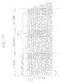
- FIG. 11 is a concept diagram schematically showing a driving method of a display device according to another exemplary embodiment of the present invention.
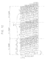
- FIG. 12 is a concept diagram schematically showing a driving method of a display device according to another exemplary embodiment of the present invention.
- FIG. 13 is a concept diagram schematically showing a driving method of a display device according to another exemplary embodiment of the present invention.
- FIG. 14 is a concept diagram schematically showing a driving method of a display device according to another exemplary embodiment of the present invention.
- FIG. 15 is a concept diagram schematically showing a driving method of a display device according to another exemplary embodiment of the present invention.
- FIG. 16 is a concept diagram schematically showing a driving method of a display device according to another exemplary embodiment of the present invention.
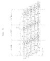
- FIG. 17 is a concept diagram schematically showing a driving method of a display device according to another exemplary embodiment of the present invention.
- FIG. 18 is a concept diagram schematically showing a driving method of a display device according to another exemplary embodiment of the present invention.
- FIG. 19 is a concept diagram schematically showing a driving method of a display device according to another exemplary embodiment of the present invention.
- FIG. 20 is a concept diagram schematically showing a driving method of a display device according to another exemplary embodiment of the present invention.
- FIG. 21 is a concept diagram schematically showing a driving method of a display device according to another exemplary embodiment of the present invention.
- FIG. 1 is a perspective view schematically explaining an operation of a display device.
- a display device includes a liquid crystal display panel 100 and a backlight unit 200 .
- the liquid crystal display panel 100 includes a plurality of liquid crystal cells 110 and 120 .
- the backlight unit 200 includes a plurality of light source substrate 220 and a plurality of light sources 210 formed on the light source substrate 220 .
- the light sources 210 in FIG. 1 are light-emitting diodes (LED).
- the light sources 210 may be an electro luminescence (EL), a cold cathode fluorescent lamp (CCFL), a hot cathode fluorescent lamp (HCFL), an external electrode fluorescent lamp (EEFL), etc.
- a scan direction D 1 pixel rows The scan direction D 1 may be a direction from an upper portion of the liquid crystal panel 100 to a lower portion of the liquid crystal panel 100 . Alternatively, the scan direction D 1 may be altered in accordance with a driving method of a display device.
- the liquid crystals in the liquid crystal cells 110 and 120 are rearranged according to an image. In FIG.
- the liquid crystal cell that a rearrangement of liquid crystal is completed is represented by reference numeral “ 110 ”
- the liquid crystal cell that a rearrangement of liquid crystal is not completed is represented by reference numeral “ 120 ”.
- the liquid crystal cell 120 that a rearrangement of liquid crystal is not completed may have an arrangement of liquid crystals of a previous frame.
- the light source 220 of the backlight unit 200 is driven to provide the liquid crystal cells 110 and 120 with light.
- the backlight unit 200 may be individually driven in each area to sequentially provide light to the liquid crystal cell 110 that the rearrangement of the liquid crystals is completed. Alternatively, the backlight unit 200 may be driven simultaneously to provide the liquid crystal cells 110 and 120 with light.
- the light source 220 may be sequentially driven along a backlight driving direction Db substantially identical to the scan direction D 1 of the liquid crystal cells 110 and 120 .
- FIG. 2 is a concept diagram schematically showing a scanning type in accordance with a first comparative embodiment.
- display device has twelve pixel rows.
- display device has more than one thousand pixel rows to display a high quality image.
- each of the pixel rows I 1 , I 2 , I 3 . . . , I 10 , I 11 and I 12 partially displays an image corresponding to the pixel rows during each of the frame intervals, and displays an image corresponding to next frame when the one frame is ended.
- a left eye image L and a right eye image R are sequentially displayed on a display in an alternating manner.
- Each of the pixel rows I 1 , I 2 , I 3 , . . . , I 10 , I 11 and I 12 is sequentially driven.
- One frame interval period is a time between a charging start time of the first pixel row and a charging start time of the last pixel row. Moreover, the one frame interval period is substantially equal to a standard charging time t of the liquid crystal cell.
- the standard charging time t of the liquid crystal cell is time required to finish rearrangement of the liquid crystals after applying a voltage to the liquid crystals.
- Light should be provided to the liquid crystal cells after charging of the pixel rows I 1 , I 2 , I 3 , . . . , I 10 , I 11 and I 12 is sufficiently completed within the one frame interval period.
- a backlight unit provides light to the liquid crystal cells at the latter part of the one frame interval period.
- An interval that the backlight unit provides light is a light providing interval Bon.
- FIG. 3 is a graph showing a charging of liquid crystals in a scanning method of FIG. 2 .
- liquid crystals are not immediately rearranged in accordance with an electric field but require a predetermined time for rearrangement of the liquid crystals. After a predetermined time period, pixels in the first pixel row I 1 is charged and an effective charging status is archived. Light should be provided from a backlight unit after an effective charging status is achieved so that a desired image may be displayed on the display device.
- the light is provided to the liquid crystal cells after a predetermined time has passed after a charging of the first pixel row I 1 for a left eye image L is started and the light is provided to the liquid crystal cells after a predetermined time has passed after a charging of the first pixel row I 1 for a right eye image R is started.
- a 3D image may be displayed on a liquid crystal display device.
- FIG. 4 is a concept diagram schematically showing a scanning type in accordance with a second comparative embodiment.
- display device has twelve pixel rows.
- each of the pixel rows I 1 , I 2 , I 3 . . . , I 10 , I 11 and I 12 is displayed.
- Each of the pixel rows I 1 , I 2 , I 3 , . . . , 110 , I 11 and I 12 partially displays an image corresponding to the rows during each of the frame intervals and displays an image corresponding to next frame when the one frame is ended.
- a left eye image L and a right eye image R are sequentially displayed on a display in an alternating manner.
- Each of the pixel rows I 1 , I 2 , I 3 , . . . , I 10 , I 11 and I 12 is sequentially driven.
- One frame interval period is a time between a charging start time of the first pixel row and a charging start time of the last pixel row.
- the one frame interval period, 1st FRAME, 2nd FRAME and 3rd FRAME is substantially equal to two times of a charging time t of the liquid crystal cell.
- Light should be provided to the liquid crystal cells after charging of the liquid crystals in the pixel rows I 1 , I 2 , I 3 , . . . , I 10 , I 11 and I 12 is sufficiently completed within the one frame interval period.
- the present exemplary embodiment has two charging time t in one frame interval period.
- a backlight unit provides light at the latter of the one frame interval period, per each pixel row.
- An interval that the backlight unit provides light is a light providing interval Bon.
- FIG. 5 is a graph showing a charging of liquid crystals in a scanning type of FIG. 4 .
- liquid crystals are not immediately rearranged in accordance with an electric field but require a predetermined time for rearranging the liquid crystals.
- the charging time ‘t’ is half of the first frame interval period, 1st FRAME.
- the light is provided from the backlight unit after a charging of the first pixel row I 1 for a left eye image L is completed because the light is provided from the backlight unit during a second charging interval.
- the liquid crystal cell in this embodiment has a twice faster charging time than the liquid crystal cell in an embodiment of FIG. 2 . Charging statuses of all the liquid crystal cells are in an effective charging status during the second charging interval, so that much correct image can be displayed.
- the light is provided from the backlight unit after a charging of the first pixel row I 1 for a right eye image R is completed, because the light is provided from the backlight unit during a second charging interval.
- a 3D image may be displayed on a liquid crystal display device.
- FIG. 6 is a concept diagram schematically showing a scanning type in accordance with a third comparative embodiment.
- each pixel rows I 1 , I 2 , I 3 , . . . , I 10 , I 11 and I 12 is sequentially driven, so that each pixel rows I 1 , I 2 , I 3 , . . . , I 10 , I 11 and I 12 are charged twice during each one frame interval period, 1st FRAME, 2nd FRAME and 3rd FRAME.
- each one frame interval period, 1st FRAME, 2nd FRAME and 3rd FRAME is substantially twice of a charging time t of the liquid crystal cell.
- Light should be provided in a stage that a charging of the pixel rows I 1 , I 2 , I 3 , . . . , I 10 , I 11 and I 12 is sufficiently completed within the one frame interval period, 1st FRAME, 2nd FRAME and 3rd FRAME.
- one frame interval period, 1st FRAME, 2nd FRAME and 3rd FRAME is twice longer than the charging time t of the liquid crystal in the present exemplary embodiment.
- a backlight unit is driven simultaneously for all pixel rows.
- the backlight unit is turned on at the latter part of the first charging time of the twelfth pixel row I 12 , and turned off before second charging time of the first pixel row I 1 is ended.
- FIG. 7 is a concept diagram schematically showing a scanning type in accordance with a fourth comparative embodiment.
- FIG. 7 it is assumed that display device has six pixel rows.
- the reason that the number of pixel rows according to a fourth comparative embodiment is different from the number of pixel rows is that a frequency of liquid crystal display according to a fourth comparative embodiment is lower than that of liquid crystal display according to another comparative embodiment.
- each of the pixel rows I 1 , I 2 , I 3 , I 4 , I 5 and I 6 partially displays an image corresponding to the pixel rows during each of the one frame interval period, 1st FRAME, 2nd FRAME and 3rd FRAME, and displays an image corresponding to next frame when the one frame interval period, 1st FRAME, 2nd FRAME and 3rd FRAME, is ended.
- FIG. 7 In order to display one frame, 1st FRAME, 2nd FRAME and 3rd FRAME, six pixel rows I 1 , I 2 , I 3 , I 4 , I 5 and I 6 are displayed.
- Each of the pixel rows I 1 , I 2 , I 3 , I 4 , I 5 and I 6 partially displays an image corresponding to the pixel rows during each of the one frame interval period, 1st FRAME, 2nd FRAME and 3rd FRAME, and displays an image corresponding to next frame when the one frame interval period, 1st
- a left eye image L and a right eye image R are sequentially displayed on a display in an alternating manner.
- Each of the pixel rows I 1 , I 2 , I 3 , I 4 , I 5 and I 6 is sequentially driven.
- One frame interval period is a time between a charging start time of the first pixel row and a charging start time of the last pixel row.
- the one frame interval period, 1st FRAME, 2nd FRAME and 3rd FRAME is substantially equal to a standard charging time t of the liquid crystal cell.
- a backlight unit is turn on at the latter part of the each one frame interval period, 1st FRAME, 2nd FRAME and 3rd FRAME, per each pixel rows.
- An interval that the backlight unit provides light is a light providing interval Bon.
- FIG. 8 is a concept diagram schematically showing a driving method of a display device according to one exemplary embodiment of the present invention.
- a driving method of a display device includes a preliminary frame charging step P 1 and a main frame charging step M 1 .
- display device has twelve pixel rows.
- display device has more than one thousand pixel rows to display a high quality image.
- a first frame 1st FRAME, a second frame 2nd FRAME and a third frame are sequentially progressed.
- Each frames, 1st FRAME, 2nd FRAME and 3rd FRAME, has substantially the same period.
- the present exemplary embodiment provides a method for displaying 3D image on a display. That is, in order to display a 3D image, a left eye image is displayed in the first frame during intervals L 1 and L 2 , and a right eye image is displayed in the second frame during intervals R 1 and R 2 . Again, a left eye image having a different sequence from the first frame is displayed in the third frame during intervals L 1 ′ and L 2 ′.
- pixel data corresponding to a (2N ⁇ 1)-th pixel row is simultaneously charged into liquid crystal cells corresponding to the (2N ⁇ 1)-th pixel row and the (2N)-th pixel row.
- An image for a left-eye is prepared the first preliminary frame charging step P 1 .
- Pixel data corresponding to the first pixel row I 1 is simultaneously charged into liquid crystal cells corresponding to a first pixel row I 1 and a second row I 2
- pixel data corresponding to the third pixel row I 3 is simultaneously charged into liquid crystal cells corresponding to a third pixel row I 3 and a fourth pixel row I 4 .
- liquid crystal cells in fifth and sixth pixel rows I 5 and I 6 are charged with data corresponding to a fifth pixel row
- seventh and eighth pixel rows I 7 and I 8 are charged with data corresponding to a seventh pixel row
- ninth and tenth pixel rows I 9 and I 10 are charged with data corresponding to a ninth pixel row
- eleventh and twelfth pixel rows I 1 and I 12 are charged with data corresponding to an eleventh pixel row.
- the main frame charging step M 1 pixel data of liquid crystal cells corresponding to the (2N ⁇ 1)-th pixel row is maintained (or hold), and a pixel data of liquid crystal cells corresponding to the (2N)-th pixel row is charged into pixel data of liquid crystal cells corresponding to the (2N)-th pixel row.
- a left eye image is prepared.
- a charging status of liquid crystal cells corresponding to the first pixel row I 1 , the third pixel row I 3 , the fifth pixel row I 5 , the seventh pixel row I 7 , the ninth pixel row I 9 and the eleventh pixel row I 11 is maintained.
- liquid crystal cells corresponding to the second pixel row I 2 is charged with data corresponding to the second pixel row I 2
- liquid crystal cells corresponding to the fourth pixel row I 4 , the sixth pixel row I 6 , the eighth pixel row I 8 , the tenth pixel row I 10 and the twelfth pixel row I 12 are charged with data corresponding to the pixel rows, respectively.
- a reversion preliminary frame charging step and a reversion main frame charging step are performed instead of the preliminary frame charging step P 1 and the main frame charging step M 1 that are performed in the first frame interval, 1st FRAME.
- the reversion preliminary frame charging step is substantially the same as the preliminary frame charging step except that pixel data is initially charged with pixel data corresponding to a (2N)-th pixel rows.
- the reversion main frame charging step is substantially the same as the main frame charging step except that pixel data of liquid crystal cells corresponding to the (2N)-th pixel row is maintained and pixel data corresponding to a (2N ⁇ 1)-th pixel row is charged with data corresponding to the pixel rows, respectively.
- a pixel data corresponding to a (2N ⁇ 1)-th pixel row is charged into a corresponding pixel group, (2N ⁇ 1)-th pixel row and (2n)th pixel row. That is, pixel data corresponding to first, third, fifth, seventh, ninth and eleventh pixel rows are charged into liquid crystal cells corresponding to second, fourth, sixth, eighth, tenth and twelfth pixel rows, respectively.
- a pixel data corresponding to a (2N)-th pixel row is charged into a corresponding pixel group, (2N ⁇ 1)-th pixel row and (2n)th pixel row. That is, pixel data corresponding to second, fourth, sixth, eighth, tenth and twelfth pixel rows are simultaneously charged into liquid crystal cells corresponding to first, third, fifth, seventh, ninth and eleventh pixel rows, respectively.
- initial pixel data which are charged during preliminary frame and reversion preliminary frame are adopted in an alternating manner. When the pixel group has more than three consecutive pixel rows, the three consecutive pixel rows in the pixel group may be charged simultaneously.
- the reversion preliminary frame charging step RP and the reversion main frame charging step RM have reversed charge sequences than the preliminary frame charging step P 1 and the main frame charging step M 1 .
- a fourth frame interval has the reversion preliminary frame charging step and the reversion main frame charging step of the second Frame.
- a fifth frame interval has the sequence identical to the first frame interval.
- a difference between a charging start time of the first pixel row and a charging start time of the last pixel row may be a half of a standard charging time (t/2) of the liquid crystal cells.
- a scanning delay time which is between a charging start time of the first pixel row and a charging start time of the last pixel row, of the present exemplary embodiment is a half of a standard charging time (t/2).
- charging of the eleventh and twelfth pixel rows I 11 and I 12 are started after a half of a standard charging time (t/2) of the liquid crystal cells is elapsed. It means that a time for charging all pixel rows of a display is a half of a standard charging time (t/2) of liquid crystal cells.
- a delay time of one frame may be reduced to about a half.
- the preliminary frame charging step P 1 and the main frame charging step M 1 may be performed during a standard charging time ‘t’ of the liquid crystal cell.
- Each of the charging steps P 1 and M 1 may be progressed during a standard charging time ‘t’ of liquid crystal cells corresponding to each pixel row.
- a charging of liquid crystal cells of one pixel row I 1 in a first pixel group (pixels in pixel rows I 1 and I 2 ) may be completed during the preliminary frame charging step P 1
- a charging of liquid crystal cells of the other pixel row I 2 in the first pixel group may be completed during the main frame charging step M 1 .
- liquid crystal cells corresponding to a (2N)-th pixel row can be charged in a short time.
- the backlight may be sequentially turned on at the latter part of the preliminary frame charging step P 1 of each pixel row and turned off before ending of the main frame charging step M 1 of each pixel row.
- a black image has to be inserted between the left eye image and the right eye image to reduce a cross-talk.
- a turn on time of a backlight unit may be extended longer than that of a conventional driving method, so that a brightness of an image may be increased.
- FIG. 9 is a concept diagram schematically showing a driving method of a display device according to another exemplary embodiment of the present invention.
- a driving of each pixel row described in FIG. 9 is substantially the same as the driving of each pixel row described in FIG. 8 except for a driving time of a backlight unit.
- the backlight unit is driven sequentially corresponding to each pixel row in an exemplary embodiment of FIG. 8 .
- the backlight unit of the driving method of FIG. 9 is turned-on simultaneously.
- the backlight may be turned on after ending of a preliminary frame charging step P 1 of the first pixel row t 1 and turned off before ending of an interval that a main frame charging step M 1 of the first pixel row I 1 .
- each of the pixels in a pixel group has a charged status which is charged by an image data of the corresponding pixel groups.
- the liquid crystal cells can be charged to their image data in a short time.
- a turn-on time of a backlight unit may be extended longer than that of a conventional driving method, so that a brightness of an image may be increased.
- the backlight unit when the backlight unit is turned on simultaneously, the backlight unit may be turned on during a short interval. As described above, the backlight unit must be turned on in a status that liquid crystal cells corresponding to each pixel row are effectively charged. An interval that the first pixel row and the last pixel row are effectively charged in the comparative embodiment of FIG. 6 is very short. Therefore, the backlight unit may be turn on for a short time, so that a luminance of a display may be decreased.
- the display device is a switchable device which can display a 2D image and a 3D image according to a source of data to be displayed, a luminance of the 3D image may be rapidly decreased.
- a difference between a driving star time of the first pixel row I 1 and a driving start time of the twelfth pixel row I 12 is a half of a start charging time ‘t’ of the liquid crystal cells, so that an effective charging interval capable of providing light to the display may be increased.
- the backlight unit is turned on after ending of a preliminary frame charging step P 1 of the first pixel row I 1 and before ending of a main frame charging step M 1 of the first pixel row I 1 .
- a total luminance according to the present exemplary embodiment may be increased rather than that of a conventional driving method.
- FIG. 10 is a concept diagram schematically showing a driving method of a display device according to another exemplary embodiment of the present invention.
- a driving method of a display device includes a preliminary frame charging step P 1 , a main frame charging step M 1 and a frame maintaining step S 1 .
- display device has twelve pixel rows. Generally, display device has more than one thousand rows to display a high quality image.
- a pixel data corresponding to a (2N ⁇ 1)-th pixel row is simultaneously charged into liquid crystal cells corresponding to the (2N ⁇ 1)-th pixel row and the (2N)-th pixel row.
- a pixel data corresponding to the first pixel row I 1 is simultaneously charged into liquid crystal cells corresponding to a first pixel row I 1 and a second pixel row I 2
- pixel data corresponding to the third pixel row I 3 is simultaneously charged into liquid crystal cells corresponding to a third pixel row I 3 and a fourth pixel row I 4 .
- liquid crystal cells in fifth and sixth pixel rows I 5 and I 6 are charged with data corresponding to a fifth pixel row
- seventh and eighth pixel rows I 7 and I 8 are charged with data corresponding to a seventh pixel row
- ninth and tenth pixel rows I 9 and I 10 are charged with data corresponding to a ninth pixel row
- eleventh and twelfth pixel rows I 11 and I 12 are charged with data corresponding to an eleventh pixel row.
- main frame charging step M 1 pixel data of liquid crystal cells corresponding to the (2N ⁇ 1)-th pixel row is maintained, and a pixel data of liquid crystal cells corresponding to the (2N)-th pixel row is charged into pixel data of liquid crystal cells corresponding to the (2N)-th pixel row.
- main frame charging step M 1 a charging status of liquid crystal cells corresponding to the first pixel row I 1 , the third pixel row I 3 , the fifth pixel row I 5 , the seventh row I 7 , the ninth pixel row I 9 and the eleventh row I 11 is maintained.
- liquid crystal cells corresponding to the second pixel row I 2 is charged with a data corresponding to the second pixel row I 2
- liquid crystal cells corresponding to the fourth pixel row I 4 , the sixth pixel row I 6 , the eighth pixel row I 8 , the tenth pixel row I 10 and the twelfth pixel row I 12 are charged with data corresponding to the pixel rows, respectively.
- a voltage charged into liquid crystal cells of all pixel rows I 1 , I 2 , I 3 , . . . , I 10 , I 11 and I 12 is maintained.
- the preliminary frame charging step P 1 and the main frame charging step M 1 are progressed during a first half of a standard charging time (t/2) of the liquid crystal cells, and the frame maintaining step S 1 is progressed during a standard charging time (t) of the liquid crystal cells.
- a difference between a charging start time of the first pixel row and a charging start time of the last pixel row may be a half of a standard charging time (t/2) of the liquid crystal cells.
- all liquid crystal cells of a display device may maintain a status that a charging is completed.
- a maintaining interval of the charging may be extended in comparison with another exemplary embodiment.
- the backlight unit may be turned on simultaneously. The backlight may be turned-on after a beginning of a main frame charging step M 1 of the last pixel row I 12 and may be turned-off before an ending of a frame maintaining step S 1 of the pixel row I 1 .
- a turn-on time of a backlight unit may be extended longer than that of a conventional backlight unit, so that a brightness of an image may be increased.
- the present exemplary embodiment may be compared with a comparative embodiment of FIG. 6 .
- the backlight turn on time cannot be extended because the backlight unit must provide light to the display device after all liquid crystal cells of a display device are charged with a voltage corresponding to an image.
- a light providing time of a backlight unit may be extended longer than that of a conventional backlight unit, so that a brightness of an image may be increased.
- a charge sequences may be reversed.
- the reversion preliminary frame charging step is a step that a pixel data corresponding to the (2N)-th pixel row is simultaneously charged into liquid crystal cells corresponding to the (2N ⁇ 1)-th pixel row and the (2N)-th pixel row.
- a voltage of liquid crystal cells corresponding to the 2N-th pixel row is maintained, and a pixel data corresponding to the (2N ⁇ 1)-th pixel row is charged into liquid crystal cells corresponding to the (2N ⁇ 1)-th pixel row.
- an image quality deterioration such as an image distortion may be prevented.
- a pixel data corresponding to a (2N ⁇ 1)-th pixel row is simultaneously charged into liquid crystal cells corresponding to the (2N ⁇ 1)-th pixel row and the (2N)-th pixel row.
- a pixel data corresponding to a (2N)-th pixel row is simultaneously charged into liquid crystal cells corresponding to the (2N ⁇ 1)-th pixel row and the (2N)-th pixel row.
- the fourth frame interval, 4th FRAME may include intervals R 1 ′ and R 2 ′ displaying each right eye image on the display device.
- FIG. 11 is a concept diagram schematically showing a driving method of a display device according to another exemplary embodiment of the present invention.
- a driving method of a display device in accordance with the present exemplary embodiment of FIG. 11 is substantially the same as the driving method of a display device in accordance with the exemplary embodiment of FIG. 8 except for at least a driving of a backlight unit.
- any repetitive detailed description may hereinafter be omitted.
- a driving method of a display device includes a preliminary frame charging step P 1 and a main frame charging step M 1 .
- a pixel data corresponding to a (2N ⁇ 1)-th pixel row is simultaneously charged into liquid crystal cells corresponding to the (2N ⁇ 1)-th pixel row and the (2N)-th pixel row.
- a pixel data corresponding to the first pixel row I 1 is simultaneously charged into liquid crystal cells corresponding to the first pixel row I 1 and the second pixel row I 2
- pixel data corresponding to the third pixel row I 3 is simultaneously charged into liquid crystal cells corresponding to the third pixel row I 3 and the fourth pixel row I 4 .
- a voltage of liquid crystal cells corresponding to the (2N ⁇ 1)-th pixel row is maintained, and a pixel data corresponding to the (2N)-th pixel row is charged into liquid crystal cells corresponding to the (2N)-th pixel row.
- a difference between a charging start time of the first pixel row and a charging start time of the last pixel row may be a half of a standard charging time (t/2) of the liquid crystal cells.
- a charging of the eleventh and twelfth pixel rows 111 and 112 are started after a half of a standard charging time (t/2) of the liquid crystal cells is elapsed from a beginning of a charging of the pixel rows I 1 and I 2 . It means that a time for charging all pixel rows of a display device is a half of a standard charging time (t/2) of liquid crystal cells. Thus, a delay time of one frame may be reduced to about a half.
- the backlight may be turned-on.
- Backlight is sequentially turned-on during the main frame charging step M 1 of each pixel row, so that the liquid crystal cells corresponding to the pixel row may display an image.
- FIG. 12 is a concept diagram schematically showing a driving method of a display device according to another exemplary embodiment of the present invention.
- a driving method of a display device includes a first preliminary frame charging step P 11 , a second preliminary frame charging step P 12 and a main frame charging step M 1 .
- a first preliminary frame charging step P 11 for convenience of description, it is assumed that display device has twelve pixel rows.
- a pixel data of a first representative pixel row among a (3N ⁇ 2)-th pixel row, a (3N ⁇ 1)-th pixel row and a 3N-th pixel row is simultaneously charged into liquid crystal cells corresponding to the (3N ⁇ 2)-th pixel row, the (3N ⁇ 1)-th pixel row and an 3N-th pixel row.
- a pixel data corresponding to the first pixel row I 1 is simultaneously charged into liquid crystal cells corresponding to the first pixel row I 1 , the second pixel row I 2 and the third pixel row I 3 .
- a pixel data corresponding to the fourth pixel row I 4 is simultaneously charged into liquid crystal cells corresponding to the fourth pixel row I 4 , the fifth pixel row I 5 and the sixth pixel row I 6 .
- the seventh, eighth and ninth pixel rows I 7 , I 8 and I 9 are charged with data corresponding to the seventh pixel row
- tenth, eleventh and twelfth pixel rows I 10 , I 11 and I 12 are charged with data corresponding to the tenth pixel row.
- Liquid crystal cells corresponding to the fourth pixel row I 4 maintain a voltage
- liquid crystal cells corresponding to the fifth pixel row I 5 and the sixth pixel row I 6 are simultaneously charged with a pixel data corresponding to the fifth pixel row I 5
- liquid crystal cells corresponding to the seventh and tenth pixel rows I 7 and I 10 maintain a voltage
- liquid crystal cells corresponding to the eighth and ninth pixel rows I 8 and I 9 are charged with a pixel data corresponding to the eighth pixel row I 8
- liquid crystal cells corresponding to the eleventh and twelfth pixel rows I 11 and I 12 are charged with a pixel data corresponding to the eleventh pixel row I 11 .
- a voltage of liquid crystal cells corresponding to the first representative pixel row and the second representative pixel row is maintained, and a pixel data corresponding to one of the remaining pixel rows is charged into liquid crystal cells corresponding to one of the remaining pixel row.
- Liquid crystal cells corresponding to the first pixel row I 1 and the second pixel row I 2 maintain a voltage
- liquid crystal cells corresponding to the third pixel row I 3 is charged with a pixel data corresponding to the third pixel row I 3
- Liquid crystal cells corresponding to the fourth pixel row I 4 and the fifth pixel row I 5 maintain a voltage
- liquid crystal cells corresponding to the sixth pixel row I 6 is charged with a pixel data corresponding to the sixth pixel row I 6 .
- liquid crystal cells corresponding to the seventh, eighth, tenth and eleventh pixel rows I 7 , I 8 , I 10 and I 11 maintain a voltage
- liquid crystal cells corresponding to the ninth pixel row I 9 is charged with a pixel data corresponding to the ninth pixel row I 9
- liquid crystal cells corresponding to the twelfth pixel row I 12 is charged with a pixel data corresponding to the twelfth pixel row I 12 .
- a difference between a charging start time of the first pixel row and a charging start time of the last pixel row may be a quarter of a standard charging time (t/4) of the liquid crystal cells.
- charging of the pixel data in tenth, eleventh and twelfth pixel rows I 10 , I 11 and I 12 are started after a quarter of a standard charging time (t/4) of the liquid crystal cells is elapsed from a beginning of a charge of the pixel data in the first, the second and the third pixel rows. It means that a time for charging all pixel rows of a display device is a quarter of a standard charging time (t/4) of liquid crystal cells. Thus, a delay time of one frame may be reduced to about a quarter.
- a driving method of a display apparatus may further include a frame maintain step S 1 which maintains voltages of liquid crystal cells corresponding to the (3N ⁇ 2)-th pixel row, the (3N ⁇ 1)-th row and an 3N-th pixel row.
- a frame maintain step S 1 which maintains voltages of liquid crystal cells corresponding to the pixel rows I 1 , I 2 , I 3 , . . . , I 10 , I 11 and I 12 are maintained.
- the first and second preliminary frame charging steps P 11 and P 12 and the main frame charging step M 1 may be progressed during a quarter of a standard charging time (t/4) of each of the liquid crystal cell.
- Each of the charging steps P 11 , P 12 and M 1 is progressed during a quarter of a standard charging time (t/4) of each of the liquid crystal cell corresponding to each pixel row.
- the frame maintaining step S 1 may be progressed during a quarter of a standard charging time (t/4) of each of the liquid crystal cell similar to the first and the second preliminary frame charging steps P 11 and P 12 and the main frame charging step M 1 .
- a sum of the charging steps P 11 , P 12 and M 1 and the maintaining step S 1 may correspond with one frame interval I FRAME.
- Liquid crystal of the display device may have a short charging time.
- the first and the second preliminary frame charging steps P 11 and P 12 , the main frame charging step M 1 and the frame maintaining step S 1 may be more than about 1 ⁇ 3 of a standard charging time of the liquid crystal cells.
- the backlight may be turned on during the main frame charging step M 1 and the frame maintaining step S 1 to display an image.
- a light may be turned on after a beginning of the main frame charging step M 1 and turned off before an ending of the frame maintaining step S 1 .
- FIG. 13 is a concept diagram schematically showing a driving method of a display device according to another exemplary embodiment of the present invention.
- a driving method of a display device in accordance with the present exemplary embodiment of FIG. 13 is substantially the same as the driving method of a display device in accordance with the exemplary embodiment of FIG. 12 except for at least a driving of a backlight unit. Thus, any repetitive detailed description may hereinafter be omitted.
- a driving method of a display apparatus may include a first preliminary frame charging step P 11 , a second preliminary frame charging step P 12 and a main frame charging step M 1 .
- the first preliminary frame charging step P 11 a pixel data of a first representative pixel row among a (3N ⁇ 2)-th pixel row, a (3N ⁇ 1)-th pixel row and a 3N-th pixel row is simultaneously charged into liquid crystal cells corresponding to the (3N ⁇ 2)-th pixel row, the (3N ⁇ 1)-th pixel row and an 3N-th pixel row.
- a voltage of liquid crystal cells corresponding to the first representative pixel row is maintained, a second representative pixel row is selected from pixel rows except for the first representative pixel row, and then a pixel data of the second representative pixel row is simultaneously charged into liquid crystal cells corresponding to remaining two pixel lines.
- the main frame charging step M 1 voltages of liquid crystal cells corresponding to the first representative pixel row and the second representative pixel row are maintained, and then a pixel data of the remaining one pixel row is simultaneously charged into liquid crystal cells corresponding to the remaining one pixel row.
- a driving method of a display apparatus may further include a frame maintain step S 1 which maintains voltages of liquid crystal cells corresponding to the (3N ⁇ -2)-th pixel row, the (3N ⁇ -1)-th pixel row and an 3N-th pixel row.
- the backlight is turned on simultaneously.
- the backlight may be turned on after an ending of the main frame charging step M 1 and before an ending of the frame maintaining step S 1 .
- FIG. 14 is a concept diagram schematically showing a driving method of a display device according to another exemplary embodiment of the present invention.
- a driving method of a display device in accordance with the present exemplary embodiment of FIG. 14 is substantially the same as the driving method of a display device in accordance with the exemplary embodiment of FIG. 13 except for at least a driving of a backlight unit.
- any repetitive detailed description may hereinafter be omitted.
- a driving method of a display apparatus may include a first preliminary frame charging step P 11 , a second preliminary frame charging step P 12 and a main frame charging step M 1 .
- the first preliminary frame charging step P 1 a pixel data of a first representative pixel row among a (3N ⁇ 2)-th pixel row, a (3N ⁇ 1)-th pixel row and a 3N-th pixel row is simultaneously charged into liquid crystal cells corresponding to the (3N ⁇ 2)-th pixel row, the (3N ⁇ 1)-th pixel row and an 3N-th pixel row.
- a voltage of liquid crystal cells corresponding to the first representative pixel row is maintained, a second representative pixel row is selected from pixel rows except for the first representative pixel row, and then a pixel data of the second representative pixel row is simultaneously charged into liquid crystal cells corresponding to remaining two pixels.
- the main frame charging step M 1 voltages of liquid crystal cells corresponding to the first representative pixel row and the second representative pixel row are maintained, and then a pixel data of the remaining one pixel row is simultaneously charged into liquid crystal cells corresponding to remaining one pixel.
- a driving method of a display apparatus may further include a frame maintain step S 1 which maintains voltages of liquid crystal cells corresponding to the (3N ⁇ 2)-th pixel row, the (3N ⁇ 1)-th pixel row and an 3N-th pixel row.
- the backlight is turned on simultaneously.
- the backlight may be turned on after a beginning of the main frame charging step M 1 and before an ending of the frame maintaining step S 1 .
- FIG. 15 is a concept diagram schematically showing a driving method of a display device according to another exemplary embodiment of the present invention.
- a driving method of a display device includes a preliminary frame charging step P 1 , a main frame charging step M 1 and a frame maintaining step S 1 .
- the preliminary frame charging step P 1 liquid crystal cells respectively corresponding to the (4N ⁇ 3)-th pixel row, the (4N ⁇ 2)-th pixel row, the (4N ⁇ 1)-th pixel row and the (4N)-th pixel row are charged with a voltage of pixel data corresponding to the (4N ⁇ 3)-th pixel row. That is, liquid crystal cells respectively corresponding to first to fourth pixel rows I 1 , I 2 , I 3 and I 4 are simultaneously charged with a voltage of pixel data corresponding to the first pixel row I 1 .
- liquid crystal cells respectively corresponding to fifth to eighth pixel rows I 5 , I 6 , I 7 and I 8 are simultaneously charged with a voltage of pixel data corresponding to the fifth pixel row I 5 .
- liquid crystal cells respectively corresponding to ninth to twelfth pixel rows I 9 , I 10 , I 11 and I 12 are simultaneously charged with a voltage of pixel data corresponding to the ninth pixel row I 9 .
- a voltage of liquid crystal cells respectively corresponding to fifth and sixth pixel rows I 5 and I 6 is maintained, and liquid crystal cells respectively corresponding to seventh and eighth pixel rows I 7 and I 8 are simultaneously charged with a voltage of a pixel data corresponding to the seventh pixel row I 7 .
- a voltage of liquid crystal cells respectively corresponding to ninth and tenth pixel rows I 9 and I 10 is maintained, and liquid crystal cells respectively corresponding to eleventh and twelfth pixel rows I 11 and I 12 are simultaneously charged with a voltage of a pixel data corresponding to the eleventh pixel row I 11 .
- a voltage of liquid crystal cells respectively corresponding to the (4N ⁇ 3)-th pixel row, the (4N ⁇ 2)-th pixel row, the (4N ⁇ 1)-th pixel row and the (4N)-th pixel row is maintained. That is, a charging voltage of all liquid crystal cells corresponding to the first to twelfth pixel rows I 1 , I 2 , I 3 , . . . , I 10 , I 11 and I 12 is maintained.
- a difference between a charging start time of the first pixel row I 1 and a charging start time of the last pixel row I 12 or a difference between a maintaining start time of the first pixel row I 1 and a maintaining start time of the last pixel row I 12 may be a quarter of a standard charging time (t/4) of the liquid crystal cells. Since a charging is progressed by four pixel rows on a display, the difference between a charging start time of the first pixel row I 1 and the last pixel row I 12 may be decreased to about 1 ⁇ 4 in comparison with a conventional art.
- the preliminary frame charging step P 1 and the main frame charging step M 1 may be about a quarter of a standard time (t/4) of the liquid crystal cell, and the frame maintaining step S 1 may be about a half of a standard time (t/2) of the liquid crystal cell.
- a sum of the preliminary frame charging step P 1 , the main frame charging step M 1 and the frame maintaining step S 1 may be substantially equal to the standard charging time ‘t’ of corresponding liquid crystal cell.
- a difference between start times or ending time of each step of the first pixel row I 1 and the last pixel row I 12 within one frame is a quarter of a standard charging time ‘t’ (t/4) of a liquid crystal cell, a delay time between each pixel rows is reduced.
- a backlight unit may be simultaneously turned on while maintaining a sufficient luminance to the display.
- the backlight may be turned on during the frame maintaining step S 1 of the first pixel row I 1 .
- the liquid crystal display panel may have a relatively lower resolution. Since a liquid crystal display device according to FIG. 7 uses a liquid crystal display panel of a low frequency, the liquid crystal display device according to FIG. 7 displays an image of a limited resolution. Moreover, since the liquid crystal display device must be turned on during an effective charging state of liquid crystals in the display, a backlight unit cannot be driven simultaneously.
- a driving method of a display device may include a preliminary frame charging step and a main frame charging step.
- the preliminary frame charging step voltages of liquid crystal cells in a pixel group including n pixel rows are charged as a pixel data of one pixel row of the pixel group.
- liquid crystal cells of a pixel row charged with pixel data of the pixel row maintain the pixel data, and liquid crystal cells of other pixel row which are not charged with pixel data of the other pixel rows are charged with pixel data of the other pixel row.
- the preliminary frame charging step is a step which simultaneously charges pixels of plural pixel rows within the pixel group with data of one of a pixel row in the pixel group.
- the main frame charging step is a step which charges pixel rows in the pixel group with data of the pixel rows. The main frame charging step is repeated until all pixel rows have its own pixel data.
- a driving method of a display device may further include a frame maintaining step S 1 which maintains a voltage of liquid crystal cells of all pixel rows.
- the frame maintaining step S 1 is a step that liquid crystal cells corresponding to each pixel row have an effective charging status. As a time of the frame maintaining step S 1 becomes longer, an interval capable of receiving light from a backlight unit becomes longer. Therefore, total luminance of a display device may be increased.
- the total time of the preliminary frame charging step, the main frame charging step and the frame maintaining step may be substantially equal to the standard charging time of the liquid crystal cells.
- FIG. 16 is a concept diagram schematically showing a driving method of a display device according to another exemplary embodiment of the present invention.
- a driving method of a display device includes frame charge-maintaining steps M 1 ′ and M 2 ′ and a frame maintaining step S 1 .
- FIG. 16 for convenience of description, it is assumed that display device has twelve pixel rows.
- liquid crystal cells corresponding to a first pixel row I 1 is charged with a corresponding pixel data of the row, and liquid crystal cells corresponding to a second pixel row I 2 maintain a charged voltages of a previous frame.
- the first, the third, the fifth, the seventh, the ninth and the eleventh pixel rows I 3 , I 5 , I 7 , I 9 and I 11 maintain a charged voltage
- the second, the fourth, the sixth, the eighth, the tenth and the twelfth pixel rows I 2 , I 4 , I 6 , I 8 , I 10 and I 12 are charged with voltages corresponding to each pixel data of the row of the present frame.
- the frame maintaining step S 1 a voltage charged into liquid crystal cells of all pixel rows I 1 , I 2 , I 3 , . . . , I 10 , I 11 and I 12 is maintained.
- the frame charge-maintaining steps M 1 ′ and M 2 ′ are progressed during a half of a standard charging time (t/2) of the liquid crystal cells, respectively.
- the frame maintaining step S 1 is progressed during a standard charging time (t) of the liquid crystal cells.
- a difference between a charging start time of the first pixel row and a charging start time of the last pixel row may be a half of a standard charging time (t/2) of the liquid crystal cells.
- the present exemplary embodiment is substantially identical to the exemplary embodiment of FIG. 10 except for at least the frame charge-maintaining step M 1 ′ and M 2 ′.
- all liquid crystal cells maintain a charged state corresponding to the image of the present frame during the frame maintaining step S 1 .
- a period having a charged state may be extended in comparison with other exemplary embodiment.
- the backlight can be turned on simultaneously while maintaining a sufficient luminance of the display.
- a difference between a charging start time of an even-numbered pixel row and a charging start time of an odd numbered pixel row is not generated in a process that it go through frame by frame at the same pixel row.
- FIG. 17 is a concept diagram schematically showing a driving method of a display device according to another exemplary embodiment of the present invention.
- FIG. 17 is substantially the same as the exemplary embodiment of FIG. 16 except that one pixel group includes three pixel rows. Thus, any repetitive detailed description may hereinafter be omitted.
- the frame charge-maintaining steps include a first frame charge-maintaining step M 1 ′, a second frame charge-maintaining step M 2 ′ and a third frame charge-maintaining step M 3 ′.
- liquid crystal cells corresponding to a first pixel row I 1 is charged with a corresponding pixel data of the present frame, and liquid crystal cells corresponding to the second and third pixel rows I 2 and I 3 maintain a charged pixel data of a previous frame.
- the fourth, seventh and tenth pixel rows I 4 , I 7 and I 10 is charged with corresponding pixel data of the present frame, respectively, and the fifth, sixth, eighth, ninth, eleventh and twelfth pixel rows I 5 , I 6 , I 8 , I 9 , I 11 and I 12 maintain charged pixel data of the previous frame, respectively.
- the first, the fourth, the seventh and the tenth pixel rows I 1 , I 4 , I 7 and I 10 which are charged with pixel data during the first frame charge-maintaining step M 1 ′ and the third, the sixth, the ninth and the eleventh pixel rows I 3 , I 6 , I 9 and I 12 which are charged with pixel data of a previous frame maintain a charged pixel data, and the second, the fifth, the eighth and the eleventh pixel rows I 2 , I 5 , I 8 and I 11 are charged with pixel data corresponding to each pixel data of the present frame.
- the frame maintaining step S 1 pixel data charged into liquid crystal cells of all pixel rows I 1 , I 2 , I 3 , . . . , I 11 and I 12 is maintained.
- the frame charge-maintaining steps M 1 ′, M 2 ′ and M 3 ′ are progressed during a quarter of a standard charging time (t/4) of the liquid crystal cells, respectively, and the frame maintaining step S 1 is progressed during a quarter of the standard charging time (T/4) of the liquid crystal cells.
- a difference between a charging start time of the first pixel row and a charging start time of the last pixel row may be a quarter of the standard charging time (t/4) of the liquid crystal cells.
- the present exemplary embodiment is substantially identical to the exemplary embodiment of FIG. 12 except for at least the frame charge-maintaining step M 1 ′, M 2 ′ and M 3 ′.
- all liquid crystal cells maintain a charged state corresponding to the image during the frame maintaining step S 1 .
- a period having a charged state may be extended in comparison with other exemplary embodiment.
- the backlight can be turned on simultaneously while maintaining a sufficient luminance of the display.
- all pixel rows are charged at the first preliminary frame charging step of one frame.
- a portion of pixel rows is charged and the remaining of pixel rows maintain pixel data of the previous frame, a corresponding pixel data is sequentially charged into each of the pixel rows.
- FIG. 18 is a concept diagram schematically showing a driving method of a display device according to another exemplary embodiment of the present invention.
- the frame black-charge-maintaining steps PB 1 and BM 1 may include a first black-charge-maintaining step PR 1 and a second black-charge-maintaining step BM 1 .
- first black-charge-maintaining step PB 1 pixel data corresponding to one pixel row is charged into the pixel row of a pixel group, for example, first, third, fifth, seventh, ninth and eleventh pixel rows I 1 , I 3 , I 5 , I 7 , I 9 and I 11 , and a voltage corresponding to a black image is charged into the other pixel rows of the pixel group, for example, second, fourth, sixth, eighth, tenth and twelfth pixel rows I 2 , I 4 , I 6 , I 8 , I 10 and I 12 .
- a voltage charged into liquid crystal cells of all pixel rows I 1 , I 2 , I 3 , . . . , I 10 , I 11 and I 12 is maintained.
- a voltage corresponding to a black image is charged into liquid crystal cells of all pixel rows I 1 , I 2 , I 3 , . . . , I 10 , I 11 and I 12 .
- the frame black-charge-maintaining steps PB 1 and BM 1 are progressed during a quarter of a standard charging time (t/4) of each of the liquid crystal cell, and the frame maintaining step S 1 is progressed during a quarter of a standard charging time (t/4) of each of the liquid crystal cell.
- a difference between a charging start time of the first pixel row and a charging start time of the last pixel row may be a quarter of a standard charging time (t/4) of the liquid crystal cells.
- FIG. 19 is substantially the same as the exemplary embodiment of FIG. 18 except that one pixel group includes three pixel rows. Thus, any repetitive detailed description may hereinafter be omitted.
- a driving method of a display device includes black-charge-maintaining steps PB 1 , PB 2 and PB 3 and a black image step B 1 .
- black-charge-maintaining steps PB 1 , PB 2 and PB 3 liquid crystal cells of one pixel row selected from a pixel group including n pixel rows are charged with corresponding pixel data of the present frame, and liquid crystal cells in the other pixel rows are charged with pixel data corresponding to a black image.
- one pixel group includes three pixel rows.
- the black-charge-maintaining steps may include a first black-charge-maintaining step PB 1 , a second black-charge-maintaining step PB 2 and a third black-charge-maintaining step PB 3 .
- liquid crystal cells of one pixel that is, first, fourth, seventh and tenth pixel rows I 1 , I 4 , I 7 and I 10 are charged with pixel data of the present frame
- liquid crystal cells of the other pixel rows that is, second, third, fifth, sixth, eighth, ninth, eleventh and twelfth pixel rows I 2 , I 3 , I 5 , I 6 , I 8 , I 9 , I 11 and I 12 are charged with a pixel data corresponding to a black image.
- the first, fourth, seventh and tenth pixel rows I 1 , I 4 , I 7 and I 10 may maintain the charged voltage
- the second, fifth, eighth and eleventh pixel rows I 2 , I 5 , I 8 and I 11 may charge pixel data corresponding to pixel row
- the third, sixth, ninth and twelfth pixel rows I 3 , I 6 , I 9 and I 12 may be charged with pixel data corresponding to a black image or maintain a charged state of the black image.
- the black image step B 1 a voltage corresponding to a black image is charged into liquid crystal cells of all pixel rows I 1 , I 2 , I 3 , . . . , I 10 , I 11 and I 12 .
- the frame black-charge-maintaining steps PB 1 , PB 2 and PB 3 are progressed during a quarter of a standard charging time (t/4) of each of the liquid crystal cell, and the black image step B 1 is progressed during a quarter of a standard charging time (t/4) of each of the liquid crystal cell.
- a difference between a charging start time of the first pixel row and a charging start time of the last pixel row may be a quarter of a standard charging time (t/4) of the liquid crystal cells.
- Exemplary embodiments of the present invention of FIGS. 18 and 19 further include a black image step.
- Pixel data of the black image are charged in the pixels prior to and after charging pixel data of the present frame.
- the black image may be inserted between images of each frame so that the quality of images may be improved.
- FIG. 20 is a concept diagram schematically showing a driving method of a display device according to another exemplary embodiment of the present invention.
- a driving method of a display device includes a preliminary frame charging step P 1 , main frame charging steps M 1 and M 2 and a black image step Bv 1 .
- display device has twelve pixel rows.
- display device may have more than one thousand pixel rows.
- display device may include pixel rows more than one thousand pixel rows.
- pixel data corresponding to a (2N ⁇ 1)-th pixel row are simultaneously charged into liquid crystal cells corresponding to the (2N ⁇ 1)-th pixel row and the (2N)-th pixel row.
- a pixel data corresponding to the first pixel row I 1 is simultaneously charged into liquid crystal cells corresponding to a first pixel row I 1 and a second pixel row I 2
- pixel data corresponding to the third pixel row I 3 is simultaneously charged into liquid crystal cells corresponding to a third pixel row I 3 and a fourth pixel row I 4 .
- fifth and sixth pixel rows I 5 and I 6 are charged with data corresponding to a fifth pixel row
- seventh and eighth pixel rows I 7 and I 8 are charged with data corresponding to a seventh pixel row
- ninth and tenth pixel rows I 9 and I 10 are charged with data corresponding to a ninth pixel row
- eleventh and twelfth pixel rows I 11 and I 12 are charged with data corresponding to an eleventh pixel row I 12 .
- a voltage of liquid crystal cells corresponding to the (2N ⁇ 1)-th pixel row is maintained, and a pixel data corresponding to the (2N)-th pixel row is charged into liquid crystal cells corresponding to the (2N)-th pixel row.
- a charging status of liquid crystal cells of the rows I 1 , I 3 , I 5 , I 7 , I 9 and I 11 is maintained.
- liquid crystal cells corresponding to the second pixel row I 2 is charged with data corresponding to the second pixel row I 2
- liquid crystal cells corresponding to the fourth pixel row I 4 , the sixth row I 6 , the eighth pixel row I 8 , the tenth pixel row I 10 and the twelfth pixel row I 12 are charged with data corresponding to a data lines, respectively.
- a duration of the black image step Bv 1 at the first pixel row is gradually increased, so that a continue time of the black image step Bv 12 is the maximum at the last pixel row.
- FIG. 21 is a concept diagram schematically showing a driving method of a display device according to another exemplary embodiment of the present invention.
- a driving method of a display device includes a preliminary frame charging step P 1 , a main frame charging step M 1 , a frame maintaining step S 1 and a black image step Bv 1 .
- display device has twelve pixel rows.
- display device may have more than one thousand pixel rows.
- display device may include pixel rows more than one thousand pixel rows.
- a driving method of a display device in accordance with the present exemplary embodiment of FIG. 21 is substantially the same as the driving method of a display device in accordance with the exemplary embodiment of FIG. 20 except that a second frame charge-maintaining step M 2 is replaced with a frame maintaining step S 1 .
- a second frame charge-maintaining step M 2 is replaced with a frame maintaining step S 1 .
- pixel data corresponding to a (2N ⁇ 1)-th pixel row are simultaneously charged into liquid crystal cells corresponding to the (2N ⁇ 1)-th pixel row and the (2N)-th pixel row.
- a pixel data corresponding to the first pixel row I 1 is simultaneously charged into liquid crystal cells corresponding to a first pixel row I 1 and a second pixel row I 2
- pixel data corresponding to the third pixel row I 3 is simultaneously charged into liquid crystal cells corresponding to a third pixel row I 3 and a fourth pixel row I 4 .
- fifth and sixth pixel rows I 5 and I 6 are charged with data corresponding to a fifth pixel row
- seventh and eighth pixel rows I 7 and I 8 are charged with data corresponding to a seventh pixel row
- ninth and tenth pixel rows I 9 and I 10 are charged with data corresponding to a ninth pixel row
- eleventh and twelfth pixel rows I 11 and I 12 are charged with data corresponding to an eleventh pixel row I 12 .
- a voltage of liquid crystal cells corresponding to the (2N ⁇ 1)-th pixel row is maintained, and a pixel data corresponding to the (2N)-th pixel row is charged into liquid crystal cells corresponding to the (2N)-th pixel row.
- a charging status of liquid crystal cells of the rows I 1 , I 3 , I 5 , I 7 , I 9 and I 11 is maintained.
- liquid crystal cells corresponding to the second pixel row I 2 is charged with data corresponding to the second pixel row I 2
- liquid crystal cells corresponding to the fourth pixel row I 4 , the sixth row I 6 , the eighth pixel row I 8 , the tenth pixel row I 10 and the twelfth pixel row I 12 are charged with data corresponding to a data lines, respectively.
- a duration of the frame maintaining step S 1 may be set to have the minimum duration at the last pixel row by being gradually decreased from the first pixel row.
- a voltage corresponding to a black image is charged into liquid crystal cells of all pixel rows I 1 , I 2 , I 3 , . . . , I 10 , I 11 and I 12 .
- a duration of the first pixel row and a duration of the last pixel row on a display device may be set different from each other.
- the black image step Bv 1 of the first pixel row may be below an average duration
- the black image step Bv 12 of the last pixel row may be over the average duration.
- a duration of the black image step Bv 1 may be set to have the maximum duration at the last pixel row by being gradually increased from the first pixel row.
- At least two pixel rows are simultaneously charged to decrease a delay time of pixel row to a half or a quarter of a standard charging time of liquid crystals, so that a 3D image may be displayed without decreasing of a vertical resolution.
- an effective charging interval that a charging of the liquid crystal cells is completed in each frame is longer than a conventional art, so that a backlight turn on time may become longer.
- a total luminance of a display device may be enhanced.
- an effective charging interval that a charging of the liquid crystal cells is completed in each frame becomes longer, so that a backlight may be turned on simultaneously while maintaining sufficient luminance of the display which reduce a manufacturing cost remarkably.
Landscapes
- Physics & Mathematics (AREA)
- Engineering & Computer Science (AREA)
- General Physics & Mathematics (AREA)
- Crystallography & Structural Chemistry (AREA)
- Chemical & Material Sciences (AREA)
- Theoretical Computer Science (AREA)
- Computer Hardware Design (AREA)
- Nonlinear Science (AREA)
- Mathematical Physics (AREA)
- Optics & Photonics (AREA)
- Microelectronics & Electronic Packaging (AREA)
- Liquid Crystal Display Device Control (AREA)
- Control Of Indicators Other Than Cathode Ray Tubes (AREA)
- Liquid Crystal (AREA)
- Controls And Circuits For Display Device (AREA)
Priority Applications (1)
| Application Number | Priority Date | Filing Date | Title |
|---|---|---|---|
| US15/267,489 US9818318B2 (en) | 2012-04-16 | 2016-09-16 | Method of driving a display device |
Applications Claiming Priority (2)
| Application Number | Priority Date | Filing Date | Title |
|---|---|---|---|
| KR1020120039317A KR20130116700A (ko) | 2012-04-16 | 2012-04-16 | 표시 장치 및 그의 구동 방법 |
| KR10-2012-0039317 | 2012-04-16 |
Related Child Applications (1)
| Application Number | Title | Priority Date | Filing Date |
|---|---|---|---|
| US15/267,489 Division US9818318B2 (en) | 2012-04-16 | 2016-09-16 | Method of driving a display device |
Publications (2)
| Publication Number | Publication Date |
|---|---|
| US20130271441A1 US20130271441A1 (en) | 2013-10-17 |
| US9460682B2 true US9460682B2 (en) | 2016-10-04 |
Family
ID=48050596
Family Applications (2)
| Application Number | Title | Priority Date | Filing Date |
|---|---|---|---|
| US13/856,280 Expired - Fee Related US9460682B2 (en) | 2012-04-16 | 2013-04-03 | Method of driving a display device |
| US15/267,489 Expired - Fee Related US9818318B2 (en) | 2012-04-16 | 2016-09-16 | Method of driving a display device |
Family Applications After (1)
| Application Number | Title | Priority Date | Filing Date |
|---|---|---|---|
| US15/267,489 Expired - Fee Related US9818318B2 (en) | 2012-04-16 | 2016-09-16 | Method of driving a display device |
Country Status (5)
| Country | Link |
|---|---|
| US (2) | US9460682B2 (ko) |
| EP (1) | EP2654035A3 (ko) |
| JP (1) | JP2013222206A (ko) |
| KR (1) | KR20130116700A (ko) |
| CN (1) | CN103377633B (ko) |
Cited By (2)
| Publication number | Priority date | Publication date | Assignee | Title |
|---|---|---|---|---|
| US20170004747A1 (en) * | 2012-04-16 | 2017-01-05 | Samsung Display Co., Ltd. | Method of driving a display device |
| US10546540B1 (en) * | 2016-09-09 | 2020-01-28 | Apple Inc. | Displays with multiple scanning modes |
Families Citing this family (7)
| Publication number | Priority date | Publication date | Assignee | Title |
|---|---|---|---|---|
| KR102175822B1 (ko) | 2014-01-03 | 2020-11-09 | 삼성디스플레이 주식회사 | 표시 장치 및 그 구동 방법 |
| KR20160017279A (ko) | 2014-08-01 | 2016-02-16 | 삼성디스플레이 주식회사 | 표시 장치 |
| KR102271628B1 (ko) | 2014-12-04 | 2021-07-02 | 삼성디스플레이 주식회사 | 표시 패널의 구동 방법 및 이를 수행하기 위한 표시 장치 |
| KR102425982B1 (ko) | 2015-09-25 | 2022-07-28 | 삼성디스플레이 주식회사 | 표시 패널의 구동 방법 및 이를 수행하는 표시 장치 |
| JP2019066733A (ja) | 2017-10-03 | 2019-04-25 | シャープ株式会社 | 液晶表示装置および液晶表示装置の駆動方法 |
| JP7463074B2 (ja) * | 2019-10-17 | 2024-04-08 | エルジー ディスプレイ カンパニー リミテッド | 表示制御装置、表示装置及び表示制御方法 |
| CN112037724B (zh) * | 2020-08-24 | 2022-07-15 | 青岛信芯微电子科技股份有限公司 | 一种图像显示方法及装置 |
Citations (10)
| Publication number | Priority date | Publication date | Assignee | Title |
|---|---|---|---|---|
| US20030179221A1 (en) | 2002-03-20 | 2003-09-25 | Hiroyuki Nitta | Display device |
| US20040041760A1 (en) * | 2002-08-30 | 2004-03-04 | Makoto Tsumura | Liquid crystal display |
| WO2007021457A2 (en) | 2005-08-09 | 2007-02-22 | Sin-Min Chang | Method and apparatus for stereoscopic display employing a transmissive active-matrix liquid crystal pixel array |
| KR20080073431A (ko) | 2007-02-06 | 2008-08-11 | 엘지디스플레이 주식회사 | 액정표시장치 및 그의 구동방법 |
| US20100020110A1 (en) * | 2007-03-28 | 2010-01-28 | Asahi Yamato | Liquid crystal display device and method for driving the same |
| CN101945298A (zh) | 2009-07-07 | 2011-01-12 | 索尼公司 | 视频显示设备和系统 |
| CN102103839A (zh) | 2009-12-17 | 2011-06-22 | 乐金显示有限公司 | 3d图像显示设备 |
| CN101604511B (zh) | 2008-06-11 | 2011-06-22 | 胜华科技股份有限公司 | 立体显示器的驱动方法 |
| US20120033053A1 (en) * | 2010-08-05 | 2012-02-09 | Joonyoung Park | Stereoscopic image display device and driving method thereof |
| US20120147069A1 (en) | 2010-12-08 | 2012-06-14 | Au Optronics Corporation | Liquid crystal display and method for driving panel thereof |
Family Cites Families (3)
| Publication number | Priority date | Publication date | Assignee | Title |
|---|---|---|---|---|
| JP2005338482A (ja) * | 2004-05-27 | 2005-12-08 | Seiko Epson Corp | 半導体集積回路 |
| JP4297100B2 (ja) * | 2004-11-10 | 2009-07-15 | セイコーエプソン株式会社 | 電気光学装置、その駆動方法および電子機器 |
| KR20130116700A (ko) * | 2012-04-16 | 2013-10-24 | 삼성디스플레이 주식회사 | 표시 장치 및 그의 구동 방법 |
-
2012
- 2012-04-16 KR KR1020120039317A patent/KR20130116700A/ko active Search and Examination
-
2013
- 2013-04-03 US US13/856,280 patent/US9460682B2/en not_active Expired - Fee Related
- 2013-04-11 EP EP13163381.0A patent/EP2654035A3/en not_active Withdrawn
- 2013-04-16 CN CN201310130565.7A patent/CN103377633B/zh not_active Expired - Fee Related
- 2013-04-16 JP JP2013085628A patent/JP2013222206A/ja active Pending
-
2016
- 2016-09-16 US US15/267,489 patent/US9818318B2/en not_active Expired - Fee Related
Patent Citations (12)
| Publication number | Priority date | Publication date | Assignee | Title |
|---|---|---|---|---|
| US20030179221A1 (en) | 2002-03-20 | 2003-09-25 | Hiroyuki Nitta | Display device |
| US20040041760A1 (en) * | 2002-08-30 | 2004-03-04 | Makoto Tsumura | Liquid crystal display |
| WO2007021457A2 (en) | 2005-08-09 | 2007-02-22 | Sin-Min Chang | Method and apparatus for stereoscopic display employing a transmissive active-matrix liquid crystal pixel array |
| KR20080073431A (ko) | 2007-02-06 | 2008-08-11 | 엘지디스플레이 주식회사 | 액정표시장치 및 그의 구동방법 |
| US20100020110A1 (en) * | 2007-03-28 | 2010-01-28 | Asahi Yamato | Liquid crystal display device and method for driving the same |
| CN101604511B (zh) | 2008-06-11 | 2011-06-22 | 胜华科技股份有限公司 | 立体显示器的驱动方法 |
| CN101945298A (zh) | 2009-07-07 | 2011-01-12 | 索尼公司 | 视频显示设备和系统 |
| US9077985B2 (en) | 2009-07-07 | 2015-07-07 | Sony Corporation | Video display device and system |
| CN102103839A (zh) | 2009-12-17 | 2011-06-22 | 乐金显示有限公司 | 3d图像显示设备 |
| US8988510B2 (en) | 2009-12-17 | 2015-03-24 | Lg Display Co., Ltd. | 3D image display device |
| US20120033053A1 (en) * | 2010-08-05 | 2012-02-09 | Joonyoung Park | Stereoscopic image display device and driving method thereof |
| US20120147069A1 (en) | 2010-12-08 | 2012-06-14 | Au Optronics Corporation | Liquid crystal display and method for driving panel thereof |
Non-Patent Citations (1)
| Title |
|---|
| European Search Report corresponding to European Patent Application No. 13163381.0, Nov. 22, 2013, 10 pages. |
Cited By (4)
| Publication number | Priority date | Publication date | Assignee | Title |
|---|---|---|---|---|
| US20170004747A1 (en) * | 2012-04-16 | 2017-01-05 | Samsung Display Co., Ltd. | Method of driving a display device |
| US9818318B2 (en) * | 2012-04-16 | 2017-11-14 | Samsung Display Co., Ltd. | Method of driving a display device |
| US10546540B1 (en) * | 2016-09-09 | 2020-01-28 | Apple Inc. | Displays with multiple scanning modes |
| US10971074B2 (en) | 2016-09-09 | 2021-04-06 | Apple Inc. | Displays with multiple scanning modes |
Also Published As
| Publication number | Publication date |
|---|---|
| EP2654035A2 (en) | 2013-10-23 |
| EP2654035A3 (en) | 2013-12-25 |
| US20130271441A1 (en) | 2013-10-17 |
| CN103377633A (zh) | 2013-10-30 |
| KR20130116700A (ko) | 2013-10-24 |
| CN103377633B (zh) | 2018-06-08 |
| JP2013222206A (ja) | 2013-10-28 |
| US9818318B2 (en) | 2017-11-14 |
| US20170004747A1 (en) | 2017-01-05 |
Similar Documents
| Publication | Publication Date | Title |
|---|---|---|
| US9818318B2 (en) | Method of driving a display device | |
| CN107863062B (zh) | 一种显示面板控制方法 | |
| CN108877641B (zh) | 一种显示面板的驱动方法和计算机可读存储介质 | |
| KR101703875B1 (ko) | 액정표시장치 및 그 구동방법 | |
| US20140125647A1 (en) | Liquid crystal display device and method of driving the same | |
| US9330592B2 (en) | Pixel structure and display device comprising the same | |
| CN108428433B (zh) | 一种oled驱动电路 | |
| US20060139281A1 (en) | Liquid crystal display device | |
| JP2003280600A (ja) | 表示装置およびその駆動方法 | |
| US20150294611A1 (en) | Displaying method and driving device of lcd panel and lcd device | |
| RU2494475C2 (ru) | Дисплейное устройство и способ управления | |
| TWI288913B (en) | Driving circuit for a display device | |
| US20170084249A1 (en) | Display apparatus and method of driving the same | |
| CN109671410B (zh) | 显示面板的驱动方法、装置、设备及存储介质 | |
| JP2009037165A (ja) | 表示装置および表示方法 | |
| CN113284427B (zh) | 显示面板及拼接显示屏 | |
| CN104050896A (zh) | 一种显示面板及其显示方法和显示装置 | |
| KR101509302B1 (ko) | 표시 장치, 표시 장치의 구동 회로 및 표시 장치의 구동 방법 | |
| US20060267897A1 (en) | Driving method for display panel and driving device thereof | |
| US9330620B2 (en) | Driving method of field sequential display | |
| CN110879500B (zh) | 显示基板及其驱动方法、显示面板、显示装置 | |
| CN113744698A (zh) | 阵列基板的驱动方法、阵列基板以及显示面板 | |
| CN110148373B (zh) | 一种显示面板、显示装置和显示面板的驱动方法 | |
| US20130335386A1 (en) | Display, image processing unit, and display method | |
| US20080238858A1 (en) | Backlight unit, display apparatus and control method thereof |
Legal Events
| Date | Code | Title | Description |
|---|---|---|---|
| AS | Assignment |
Owner name: SAMSUNG DISPLAY CO., LTD., KOREA, REPUBLIC OF Free format text: ASSIGNMENT OF ASSIGNORS INTEREST;ASSIGNORS:AHN, IK-HYUN;PARK, BONG-IM;KIM, SEON-KI;AND OTHERS;SIGNING DATES FROM 20130310 TO 20130311;REEL/FRAME:030146/0012 |
|
| FEPP | Fee payment procedure |
Free format text: PAYOR NUMBER ASSIGNED (ORIGINAL EVENT CODE: ASPN); ENTITY STATUS OF PATENT OWNER: LARGE ENTITY |
|
| STCF | Information on status: patent grant |
Free format text: PATENTED CASE |
|
| FEPP | Fee payment procedure |
Free format text: MAINTENANCE FEE REMINDER MAILED (ORIGINAL EVENT CODE: REM.); ENTITY STATUS OF PATENT OWNER: LARGE ENTITY |
|
| LAPS | Lapse for failure to pay maintenance fees |
Free format text: PATENT EXPIRED FOR FAILURE TO PAY MAINTENANCE FEES (ORIGINAL EVENT CODE: EXP.); ENTITY STATUS OF PATENT OWNER: LARGE ENTITY |
|
| STCH | Information on status: patent discontinuation |
Free format text: PATENT EXPIRED DUE TO NONPAYMENT OF MAINTENANCE FEES UNDER 37 CFR 1.362 |
|
| FP | Lapsed due to failure to pay maintenance fee |
Effective date: 20201004 |