US9323258B2 - Voltage regulator - Google Patents
Voltage regulator Download PDFInfo
- Publication number
- US9323258B2 US9323258B2 US14/639,681 US201514639681A US9323258B2 US 9323258 B2 US9323258 B2 US 9323258B2 US 201514639681 A US201514639681 A US 201514639681A US 9323258 B2 US9323258 B2 US 9323258B2
- Authority
- US
- United States
- Prior art keywords
- circuit
- voltage
- output
- current
- detection circuit
- Prior art date
- Legal status (The legal status is an assumption and is not a legal conclusion. Google has not performed a legal analysis and makes no representation as to the accuracy of the status listed.)
- Expired - Fee Related
Links
- 238000001514 detection method Methods 0.000 claims abstract description 54
- 230000001105 regulatory effect Effects 0.000 claims abstract description 36
- 230000001629 suppression Effects 0.000 description 11
- 238000010586 diagram Methods 0.000 description 7
- 230000000694 effects Effects 0.000 description 4
- 230000001276 controlling effect Effects 0.000 description 1
- 230000003247 decreasing effect Effects 0.000 description 1
- 229920006395 saturated elastomer Polymers 0.000 description 1
Images


Classifications
-
- G—PHYSICS
- G05—CONTROLLING; REGULATING
- G05F—SYSTEMS FOR REGULATING ELECTRIC OR MAGNETIC VARIABLES
- G05F1/00—Automatic systems in which deviations of an electric quantity from one or more predetermined values are detected at the output of the system and fed back to a device within the system to restore the detected quantity to its predetermined value or values, i.e. retroactive systems
- G05F1/10—Regulating voltage or current
- G05F1/46—Regulating voltage or current wherein the variable actually regulated by the final control device is dc
- G05F1/56—Regulating voltage or current wherein the variable actually regulated by the final control device is dc using semiconductor devices in series with the load as final control devices
- G05F1/575—Regulating voltage or current wherein the variable actually regulated by the final control device is dc using semiconductor devices in series with the load as final control devices characterised by the feedback circuit
-
- H—ELECTRICITY
- H02—GENERATION; CONVERSION OR DISTRIBUTION OF ELECTRIC POWER
- H02M—APPARATUS FOR CONVERSION BETWEEN AC AND AC, BETWEEN AC AND DC, OR BETWEEN DC AND DC, AND FOR USE WITH MAINS OR SIMILAR POWER SUPPLY SYSTEMS; CONVERSION OF DC OR AC INPUT POWER INTO SURGE OUTPUT POWER; CONTROL OR REGULATION THEREOF
- H02M1/00—Details of apparatus for conversion
- H02M1/32—Means for protecting converters other than automatic disconnection
Definitions
- the present invention relates to an overshoot suppression circuit for a voltage regulator.
- FIG. 4 is a circuit diagram illustrating the conventional voltage regulator.
- the conventional voltage regulator includes a reference voltage circuit 101 , an error amplifier circuit 102 , a bias circuit 103 for the error amplifier circuit 102 , a PMOS transistor 104 serving as an output transistor, a voltage dividing resistor circuit 105 , an amplifier 301 , a bias circuit 302 for the amplifier 301 , and a PMOS transistor 108 .
- the PMOS transistor 104 is connected between a power supply terminal and an output terminal 109 .
- the voltage dividing resistor circuit 105 for outputting a feedback voltage Vfb is connected between the output terminal 109 and a ground terminal.
- the error amplifier circuit 102 has an inverting input terminal connected to the reference voltage circuit 101 , a non-inverting input terminal for inputting the feedback voltage Vfb, and an output terminal connected to a gate of the PMOS transistor 104 .
- the bias circuit 103 supplies an operating current to the error amplifier circuit 102 .
- the PMOS transistor 108 is connected between the power supply terminal and the gate of the PMOS transistor 104 .
- the amplifier 301 has a non-inverting input terminal connected to the reference voltage circuit 101 , an inverting input terminal for inputting the feedback voltage Vfb, and an output terminal connected to a gate of the PMOS transistor 108 .
- the bias circuit 302 supplies an operating current to the amplifier 301 .
- the amplifier 301 compares the input feedback voltage Vfb with a reference voltage Vref. When the feedback voltage Vfb is lower than the reference voltage Vref, the amplifier 301 outputs a Hi signal to turn OFF the PMOS transistor 108 . When an overshoot occurs in an output voltage Vout of the output terminal 109 and the feedback voltage Vfb becomes higher than the reference voltage Vref, the amplifier 301 outputs a Lo signal to turn ON the PMOS transistor 108 .
- the conventional voltage regulator operates in the manner described above to prevent the overshoot in the output voltage Vout of the output terminal 109 from being larger (see, for example, Japanese Patent Application Laid-open No. 2005-301439).
- non-regulated state a voltage lower than a predetermined output voltage Vout
- the present invention has been made in view of the above-mentioned problems, and provides a voltage regulator that is low in current consumption and is capable of suppressing the occurrence of an excessive overshoot at an output terminal when a power supply voltage becomes high in a non-regulated state.
- a voltage regulator including an overshoot suppression circuit is configured as follows.
- the voltage regulator includes: an overshoot limiting circuit for detecting an occurrence of an overshoot in an output voltage and limiting a current of an output transistor; and a non-regulated state detection circuit for detecting that the voltage regulator is in a non-regulated state based on a voltage of an output terminal and a current flowing through the output transistor.
- the overshoot limiting circuit has an operating current controlled by a detection signal of the non-regulated state detection circuit.
- the voltage regulator including the overshoot suppression circuit according to one embodiment of the present invention has the effect that the current consumption is low and the overshoot of the output voltage that occurs when the power supply voltage becomes high in the non-regulated state can be suppressed.
- FIG. 1 is a circuit diagram of a voltage regulator including an overshoot suppression circuit according to a first embodiment of the present invention
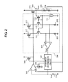
- FIG. 2 is a circuit diagram of a voltage regulator including an overshoot suppression circuit according to a second embodiment of the present invention
- FIG. 3 is a circuit diagram illustrating an exemplary overshoot control circuit according to the embodiments of the present invention.
- FIG. 4 is a circuit diagram of a conventional voltage regulator including an overshoot suppression circuit.
- FIG. 1 is a circuit diagram of a voltage regulator including an overshoot suppression circuit according to a first embodiment of the present invention.
- the voltage regulator includes a reference voltage circuit 101 , an error amplifier circuit 102 , a bias circuit 103 for the error amplifier circuit 102 , an output transistor 104 , a voltage dividing resistor circuit 105 , a non-regulated state detection circuit 106 , an overshoot control circuit 107 , and a PMOS transistor 108 .
- the non-regulated state detection circuit 106 and the overshoot control circuit 107 constitute the overshoot suppression circuit.
- the voltage dividing resistor circuit 105 is connected between an output terminal 109 and a ground terminal.
- the error amplifier circuit 102 has a non-inverting input terminal for inputting a feedback voltage Vfb and an inverting input terminal for inputting a reference voltage Vref.
- the output transistor 104 has a gate connected to an output terminal of the error amplifier circuit 102 , a source connected to a power supply terminal, and a drain connected to the output terminal 109 .
- the non-regulated state detection circuit 106 inputs a voltage of the output terminal 109 and a voltage of the power supply terminal, and has an output terminal connected to the overshoot control circuit 107 .
- the overshoot control circuit 107 inputs the feedback voltage Vfb and the reference voltage Vref, and has output terminals connected to the bias circuit 103 and a gate of the PMOS transistor 108 .
- the voltage dividing resistor circuit 105 divides an output voltage Vout of the output terminal 109 to output the feedback voltage Vfb.
- the error amplifier circuit 102 compares the feedback voltage Vfb with the reference voltage Vref output from the reference voltage circuit 101 .
- the output transistor 104 is controlled by an output voltage of the error amplifier circuit 102 , and has the function of maintaining the voltage of the output terminal 109 to be constant.
- the non-regulated state detection circuit 106 detects a non-regulated state based on a current flowing through the output transistor 104 and the output voltage Vout of the output terminal 109 .
- the overshoot control circuit 107 detects an overshoot at the output terminal 109 based on the reference voltage Vref and the feedback voltage Vfb, and controls the PMOS transistor 108 and the bias circuit 103 . In response to a detection signal Vdet of the non-regulated state detection circuit 106 , the overshoot control circuit 107 controls an operating current of the overshoot control circuit 107 .
- the overshoot control circuit 107 is formed of a circuit illustrated in FIG. 3 , for example.
- the overshoot control circuit 107 illustrated in FIG. 3 includes an amplifier 301 for inputting the reference voltage Vref and the feedback voltage Vfb, and a bias circuit 302 for inputting the detection signal Vdet of the non-regulated state detection circuit 106 and controlling an operating current of the amplifier 301 .
- the overshoot control circuit 107 only needs to be a circuit for realizing the function of detecting an overshoot at the output terminal 109 , and the circuit configuration is not particularly limited. Further, the bias circuit 103 only needs to be a constant current circuit for increasing the current in response to a signal of the overshoot control circuit 107 , and the circuit configuration is not particularly limited.
- the non-regulated state detection circuit 106 includes PMOS transistors 110 , 112 , 113 , 116 , 117 , 120 , and 121 , NMOS transistors 114 , 115 , 118 , and 119 , and a constant current source 111 .
- the PMOS transistor 110 has a source connected to the output terminal 109 , and a gate and a drain connected to the constant current source 111 .
- the PMOS transistor 112 has a source connected to a drain of the PMOS transistor 113 , a gate connected to the gate and the drain of the PMOS transistor 110 , and a drain connected to a gate and a drain of the NMOS transistor 114 .
- the PMOS transistor 113 has a source connected to the power supply terminal, and a gate connected to the output terminal of the error amplifier circuit 102 .
- the NMOS transistor 114 has a source connected to the ground terminal, and a gate and a drain connected to a gate of the NMOS transistor 115 .
- the PMOS transistor 116 has a source connected to a drain of the PMOS transistor 117 , a gate connected to the gate and the drain of the PMOS transistor 110 , and a drain connected to a gate and a drain of the NMOS transistor 118 .
- the PMOS transistor 117 has a source connected to the power supply terminal, and a gate connected to the output terminal of the error amplifier circuit 102 .
- the NMOS transistor 118 has a source connected to the ground terminal, and a gate and a drain connected to a gate of the NMOS transistor 119 .
- the NMOS transistor 119 has a source connected to the ground terminal, and a drain connected to a gate and a drain of the PMOS transistor 120 .
- the PMOS transistor 120 has a source connected to the power supply terminal, and a gate and a drain connected to a gate of the PMOS transistor 121 .
- the PMOS transistor 121 and the NMOS transistor 115 are connected between the power supply terminal and the ground terminal, and a connection node thereof is the output terminal of the non-regulated state detection circuit 106 .
- the PMOS transistor 110 and the constant current source 111 detect a state of the output terminal 109 .
- the PMOS transistor 112 , the PMOS transistor 113 , and the NMOS transistor 114 constitute a first detection circuit.
- the first detection circuit outputs a detection result of the state of the output terminal 109 to the gate of the NMOS transistor 115 .
- the PMOS transistor 116 , the PMOS transistor 117 , the NMOS transistor 118 , the NMOS transistor 119 , and the PMOS transistor 120 constitute a second detection circuit.
- the second detection circuit outputs the detection result of the state of the output terminal 109 to the gate of the PMOS transistor 121 .
- the currents to be supplied by the PMOS transistor 121 and the NMOS transistor 115 are changed in accordance with the signals input to the respective gates thereof, and the signal Vdet is output to the output terminal of the non-regulated state detection circuit 106 based on a balance of the currents.
- the above-mentioned overshoot suppression circuit operates as follows to suppress an overshoot at the output terminal 109 .
- normal state The state in which the power supply voltage is sufficiently high and the output voltage Vout of the output terminal 109 is close to a predetermined voltage.
- non-regulated state The state in which the power supply voltage is low and the output terminal 109 outputs a voltage lower than a predetermined output voltage Vout.
- Each transistor in the non-regulated state detection circuit 106 is designed as follows, for example.
- the PMOS transistor 113 and the PMOS transistor 117 for mirroring a current of the output transistor 104 are designed so that the PMOS transistor 113 has a larger mirror ratio.
- the PMOS transistor 112 and the PMOS transistor 116 for minoring a current of the PMOS transistor 110 are designed so that the PMOS transistor 116 has a larger mirror ratio.
- the PMOS transistors 112 , 113 , 116 , and 117 are designed so that the currents supplied by the PMOS transistor 112 and the PMOS transistor 116 are sufficiently larger than the currents supplied by the PMOS transistor 113 and the PMOS transistor 117 in the normal state.
- the non-regulated state detection circuit 106 outputs a signal Vdet of Lo to the output terminal, thereby indicating that the output transistor 104 is in a saturated state.
- the overshoot control circuit 107 reduces the operating current to enter the normal state.
- the difference between the power supply voltage and the output voltage Vout is reduced.
- the output voltage Vout is low, and hence a voltage of Lo is input to the gates of the PMOS transistor 113 and the PMOS transistor 117 so that the PMOS transistor 113 and the PMOS transistor 117 are turned ON. Accordingly, drain voltages of the PMOS transistor 113 and the PMOS transistor 117 become the power supply voltage. In other words, the drain voltages of the PMOS transistor 113 and the PMOS transistor 117 become closer to the output voltage Vout. Even with the low output voltage Vout, the PMOS transistor 110 allows a current to flow because the current supplied from the bias circuit 111 is sufficiently small.
- a gate voltage of the PMOS transistor 110 becomes a voltage corresponding to the impedance of the bias circuit 111 and the PMOS transistor 110 and the output voltage Vout. Then, gate voltages of the PMOS transistor 112 and the PMOS transistor 116 are equal to the gate voltage of the PMOS transistor 110 . Further, source voltages of the PMOS transistor 112 and the PMOS transistor 116 are determined by the gate voltage of the PMOS transistor 110 and thresholds of the PMOS transistor 112 and the PMOS transistor 116 .
- the currents supplied by the PMOS transistor 112 and the PMOS transistor 116 are smaller than the currents supplied by the PMOS transistor 113 and the PMOS transistor 117 . Accordingly, the PMOS transistor 116 allows a larger current to flow than the current of the PMOS transistor 112 because the mirror ratio of the PMOS transistor 116 is larger than that of the PMOS transistor 112 . As a result of mirroring those currents, the PMOS transistor 121 allows a larger current to flow than the current of the NMOS transistor 115 . Accordingly, the non-regulated state detection circuit 106 outputs a signal Vdet of Hi to the output terminal, thereby indicating that the voltage regulator is in the non-regulated state.
- the overshoot control circuit 107 increases the operating current to enter a high-speed operating state. Accordingly, even when the power supply voltage is increased from this state and an overshoot occurs at the output terminal 109 , the overshoot control circuit 107 can detect the overshoot quickly to control the bias circuit 103 and the PMOS transistor 108 . Consequently, the overshoot at the output terminal 109 can be suppressed.
- the overshoot suppression circuit for the voltage regulator enters, in the normal state, a low consumption state in which the operating current of the overshoot control circuit 107 is small, and hence the current consumption can be reduced.
- the non-regulated state detection circuit 106 detects the non-regulated state of the voltage regulator, the operating current of the overshoot control circuit 107 is increased, and hence the overshoot at the output terminal 109 can be suppressed quickly.
- FIG. 2 illustrates a circuit diagram of a voltage regulator according to a second embodiment of the present invention.
- the non-regulated state detection circuit 106 is configured as follows.
- the first detection circuit is formed of the PMOS transistor 112 , the PMOS transistor 113 , and a resistor 202 .
- the second detection circuit is formed of the PMOS transistor 116 , the PMOS transistor 117 , and a resistor 203 .
- An output terminal of a comparator circuit 201 for inputting respective detection results serves as the output terminal of the non-regulated state detection circuit 106 .
- the voltage regulator according to the embodiments of the present invention is configured so that, when an overshoot is detected, the current of the output transistor 104 is decreased while the current of the bias circuit 103 is increased in response to the signal from the overshoot control circuit 107 .
- the effect of suppressing the overshoot can be obtained, and hence the present invention is not limited to the configuration described above.
Landscapes
- Engineering & Computer Science (AREA)
- Physics & Mathematics (AREA)
- Electromagnetism (AREA)
- General Physics & Mathematics (AREA)
- Radar, Positioning & Navigation (AREA)
- Automation & Control Theory (AREA)
- Power Engineering (AREA)
- Continuous-Control Power Sources That Use Transistors (AREA)
Abstract
Description
Claims (2)
Applications Claiming Priority (3)
| Application Number | Priority Date | Filing Date | Title |
|---|---|---|---|
| JP2012-197541 | 2012-09-07 | ||
| JP2012197541A JP6130112B2 (en) | 2012-09-07 | 2012-09-07 | Voltage regulator |
| PCT/JP2013/068815 WO2014038284A1 (en) | 2012-09-07 | 2013-07-10 | Voltage regulator |
Related Parent Applications (1)
| Application Number | Title | Priority Date | Filing Date |
|---|---|---|---|
| PCT/JP2013/068815 Continuation WO2014038284A1 (en) | 2012-09-07 | 2013-07-10 | Voltage regulator |
Publications (2)
| Publication Number | Publication Date |
|---|---|
| US20150177752A1 US20150177752A1 (en) | 2015-06-25 |
| US9323258B2 true US9323258B2 (en) | 2016-04-26 |
Family
ID=50236902
Family Applications (1)
| Application Number | Title | Priority Date | Filing Date |
|---|---|---|---|
| US14/639,681 Expired - Fee Related US9323258B2 (en) | 2012-09-07 | 2015-03-05 | Voltage regulator |
Country Status (7)
| Country | Link |
|---|---|
| US (1) | US9323258B2 (en) |
| EP (1) | EP2894537B1 (en) |
| JP (1) | JP6130112B2 (en) |
| KR (1) | KR102052896B1 (en) |
| CN (1) | CN104603710B (en) |
| TW (1) | TWI582562B (en) |
| WO (1) | WO2014038284A1 (en) |
Cited By (4)
| Publication number | Priority date | Publication date | Assignee | Title |
|---|---|---|---|---|
| US20150061757A1 (en) * | 2013-08-28 | 2015-03-05 | Mediatek Singapore Pte. Ltd. | Low dropout linear regulators and starting methods therefor |
| US20160105113A1 (en) * | 2013-06-25 | 2016-04-14 | Seiko Instruments Inc. | Voltage regulator |
| US10747247B2 (en) * | 2016-12-22 | 2020-08-18 | New Japan Radio Co., Ltd. | Power supply circuit |
| US11567522B2 (en) | 2016-11-15 | 2023-01-31 | Realtek Semiconductor Corporation | Voltage reference buffer circuit |
Families Citing this family (13)
| Publication number | Priority date | Publication date | Assignee | Title |
|---|---|---|---|---|
| CN104142701B (en) | 2013-05-06 | 2016-08-24 | 意法半导体研发(深圳)有限公司 | Current-limiting circuit |
| JP6513943B2 (en) * | 2014-12-19 | 2019-05-15 | エイブリック株式会社 | Voltage regulator |
| DE102015216928B4 (en) | 2015-09-03 | 2021-11-04 | Dialog Semiconductor (Uk) Limited | Overvoltage clamp controller and procedures |
| US9645594B2 (en) * | 2015-10-13 | 2017-05-09 | STMicroelectronics Design & Application S.R.O. | Voltage regulator with dropout detector and bias current limiter and associated methods |
| US10031541B1 (en) * | 2017-07-05 | 2018-07-24 | Infineon Technologies Ag | Current sensing for linear voltage regulator |
| TWI633408B (en) | 2017-08-17 | 2018-08-21 | 力晶科技股份有限公司 | Voltage regulation device |
| KR101937268B1 (en) * | 2017-10-11 | 2019-04-09 | 현대오트론 주식회사 | Real-time slope control appartus for voltage regulator and operating method thereof |
| JP6986999B2 (en) * | 2018-03-15 | 2021-12-22 | エイブリック株式会社 | Voltage regulator |
| JP7065660B2 (en) * | 2018-03-22 | 2022-05-12 | エイブリック株式会社 | Voltage regulator |
| CN110134176B (en) * | 2018-09-05 | 2024-05-28 | 江西联智集成电路有限公司 | LDO circuit and wireless charging system |
| CN110221647B (en) * | 2019-06-28 | 2020-09-08 | 上海视欧光电科技有限公司 | Voltage stabilizer |
| JP7391791B2 (en) * | 2020-08-12 | 2023-12-05 | 株式会社東芝 | constant voltage circuit |
| JP2023018250A (en) * | 2021-07-27 | 2023-02-08 | ローム株式会社 | linear regulator circuit |
Citations (10)
| Publication number | Priority date | Publication date | Assignee | Title |
|---|---|---|---|---|
| JP2001022455A (en) | 1999-07-09 | 2001-01-26 | New Japan Radio Co Ltd | Regulator circuit |
| JP2003330555A (en) | 2002-05-14 | 2003-11-21 | Renesas Technology Corp | Semiconductor integrated circuit and ic card |
| JP2005301439A (en) | 2004-04-07 | 2005-10-27 | Ricoh Co Ltd | Voltage regulator |
| JP2006301787A (en) | 2005-04-18 | 2006-11-02 | Ricoh Co Ltd | Constant-voltage power supply circuit |
| US20070115045A1 (en) * | 2003-08-07 | 2007-05-24 | Toshihisa Nagata | Constant voltage circuit |
| US20080265852A1 (en) * | 2007-04-27 | 2008-10-30 | Takashi Imura | Voltage regulator |
| JP2009146130A (en) | 2007-12-13 | 2009-07-02 | Oki Semiconductor Co Ltd | Dropper type regulator |
| US20090189584A1 (en) * | 2008-01-24 | 2009-07-30 | Teruo Suzuki | Voltage regulator |
| JP2009199501A (en) | 2008-02-25 | 2009-09-03 | Seiko Instruments Inc | Voltage regulator |
| US8072198B2 (en) * | 2009-02-10 | 2011-12-06 | Seiko Instruments Inc. | Voltage regulator |
Family Cites Families (8)
| Publication number | Priority date | Publication date | Assignee | Title |
|---|---|---|---|---|
| DE3723579C1 (en) * | 1987-07-16 | 1989-02-16 | Sgs Halbleiterbauelemente Gmbh | Longitudinal voltage regulator |
| JP2001306163A (en) * | 2000-04-27 | 2001-11-02 | Matsushita Electric Ind Co Ltd | Regulator circuit with protective function by analog mos against excess current |
| JP4050671B2 (en) * | 2003-01-08 | 2008-02-20 | 株式会社リコー | Constant voltage circuit |
| JP2006139673A (en) * | 2004-11-15 | 2006-06-01 | Seiko Instruments Inc | Voltage regulator |
| JP4892366B2 (en) * | 2007-02-01 | 2012-03-07 | セイコーインスツル株式会社 | Overcurrent protection circuit and voltage regulator |
| JP4929043B2 (en) * | 2007-05-15 | 2012-05-09 | 株式会社リコー | Overcurrent protection circuit and electronic device provided with the overcurrent protection circuit |
| JP5279544B2 (en) * | 2009-02-17 | 2013-09-04 | セイコーインスツル株式会社 | Voltage regulator |
| JP5828206B2 (en) * | 2011-01-24 | 2015-12-02 | 凸版印刷株式会社 | Constant voltage circuit |
-
2012
- 2012-09-07 JP JP2012197541A patent/JP6130112B2/en not_active Expired - Fee Related
-
2013
- 2013-07-10 CN CN201380046042.2A patent/CN104603710B/en not_active Expired - Fee Related
- 2013-07-10 WO PCT/JP2013/068815 patent/WO2014038284A1/en unknown
- 2013-07-10 KR KR1020157005713A patent/KR102052896B1/en active IP Right Grant
- 2013-07-10 EP EP13835676.1A patent/EP2894537B1/en active Active
- 2013-07-22 TW TW102126099A patent/TWI582562B/en active
-
2015
- 2015-03-05 US US14/639,681 patent/US9323258B2/en not_active Expired - Fee Related
Patent Citations (10)
| Publication number | Priority date | Publication date | Assignee | Title |
|---|---|---|---|---|
| JP2001022455A (en) | 1999-07-09 | 2001-01-26 | New Japan Radio Co Ltd | Regulator circuit |
| JP2003330555A (en) | 2002-05-14 | 2003-11-21 | Renesas Technology Corp | Semiconductor integrated circuit and ic card |
| US20070115045A1 (en) * | 2003-08-07 | 2007-05-24 | Toshihisa Nagata | Constant voltage circuit |
| JP2005301439A (en) | 2004-04-07 | 2005-10-27 | Ricoh Co Ltd | Voltage regulator |
| JP2006301787A (en) | 2005-04-18 | 2006-11-02 | Ricoh Co Ltd | Constant-voltage power supply circuit |
| US20080265852A1 (en) * | 2007-04-27 | 2008-10-30 | Takashi Imura | Voltage regulator |
| JP2009146130A (en) | 2007-12-13 | 2009-07-02 | Oki Semiconductor Co Ltd | Dropper type regulator |
| US20090189584A1 (en) * | 2008-01-24 | 2009-07-30 | Teruo Suzuki | Voltage regulator |
| JP2009199501A (en) | 2008-02-25 | 2009-09-03 | Seiko Instruments Inc | Voltage regulator |
| US8072198B2 (en) * | 2009-02-10 | 2011-12-06 | Seiko Instruments Inc. | Voltage regulator |
Non-Patent Citations (1)
| Title |
|---|
| International Search Report, and English language translation thereof, in corresponding International Application No. PCT/JP2013/068815, dated Aug. 13, 2013, 10 pages. |
Cited By (6)
| Publication number | Priority date | Publication date | Assignee | Title |
|---|---|---|---|---|
| US20160105113A1 (en) * | 2013-06-25 | 2016-04-14 | Seiko Instruments Inc. | Voltage regulator |
| US10177655B2 (en) * | 2013-06-25 | 2019-01-08 | Ablic Inc. | Voltage regulator including a non-regulated state detection circuit |
| US20150061757A1 (en) * | 2013-08-28 | 2015-03-05 | Mediatek Singapore Pte. Ltd. | Low dropout linear regulators and starting methods therefor |
| US9977443B2 (en) | 2013-08-28 | 2018-05-22 | Mediatek Singapore Pte. Ltd. | Low dropout linear regulators and starting methods therefor |
| US11567522B2 (en) | 2016-11-15 | 2023-01-31 | Realtek Semiconductor Corporation | Voltage reference buffer circuit |
| US10747247B2 (en) * | 2016-12-22 | 2020-08-18 | New Japan Radio Co., Ltd. | Power supply circuit |
Also Published As
| Publication number | Publication date |
|---|---|
| JP6130112B2 (en) | 2017-05-17 |
| EP2894537B1 (en) | 2020-02-26 |
| US20150177752A1 (en) | 2015-06-25 |
| TWI582562B (en) | 2017-05-11 |
| CN104603710B (en) | 2016-10-12 |
| KR102052896B1 (en) | 2019-12-06 |
| CN104603710A (en) | 2015-05-06 |
| EP2894537A4 (en) | 2016-04-27 |
| KR20150048763A (en) | 2015-05-07 |
| EP2894537A1 (en) | 2015-07-15 |
| WO2014038284A1 (en) | 2014-03-13 |
| TW201423302A (en) | 2014-06-16 |
| JP2014052886A (en) | 2014-03-20 |
Similar Documents
| Publication | Publication Date | Title |
|---|---|---|
| US9323258B2 (en) | Voltage regulator | |
| US9141121B2 (en) | Voltage regulator | |
| US8957659B2 (en) | Voltage regulator | |
| US7948223B2 (en) | Constant voltage circuit using plural error amplifiers to improve response speed | |
| US7821242B2 (en) | Constant voltage circuit and method of controlling ouput voltage of constant voltage circuit | |
| US9857817B2 (en) | Sink/source output stage with operating point current control circuit for fast transient loading | |
| JP4953246B2 (en) | Voltage regulator | |
| JP5987206B2 (en) | Voltage regulator circuit arrangement and associated operating method | |
| US7199566B2 (en) | Voltage regulator | |
| US8742819B2 (en) | Current limiting circuitry and method for pass elements and output stages | |
| US9831757B2 (en) | Voltage regulator | |
| US9236732B2 (en) | Voltage regulator | |
| TWI801493B (en) | voltage regulator | |
| US20150188421A1 (en) | Voltage regulator | |
| US10175708B2 (en) | Power supply device | |
| US9886052B2 (en) | Voltage regulator | |
| US9720428B2 (en) | Voltage regulator | |
| US9946276B2 (en) | Voltage regulators with current reduction mode | |
| US20130241508A1 (en) | Voltage regulator | |
| US9891642B2 (en) | Current source and current supply system with hysteresis |
Legal Events
| Date | Code | Title | Description |
|---|---|---|---|
| AS | Assignment |
Owner name: SEIKO INSTRUMENTS INC., JAPAN Free format text: ASSIGNMENT OF ASSIGNORS INTEREST;ASSIGNORS:NAKASHIMO, TAKAO;KUROZO, TADASHI;REEL/FRAME:035152/0603 Effective date: 20150120 |
|
| AS | Assignment |
Owner name: SII SEMICONDUCTOR CORPORATION ., JAPAN Free format text: ASSIGNMENT OF ASSIGNORS INTEREST;ASSIGNOR:SEIKO INSTRUMENTS INC;REEL/FRAME:037783/0166 Effective date: 20160209 |
|
| AS | Assignment |
Owner name: SII SEMICONDUCTOR CORPORATION, JAPAN Free format text: CORRECTIVE ASSIGNMENT TO CORRECT THE EXECUTION DATE PREVIOUSLY RECORDED AT REEL: 037783 FRAME: 0166. ASSIGNOR(S) HEREBY CONFIRMS THE ASSIGNMENT;ASSIGNOR:SEIKO INSTRUMENTS INC;REEL/FRAME:037903/0928 Effective date: 20160201 |
|
| STCF | Information on status: patent grant |
Free format text: PATENTED CASE |
|
| AS | Assignment |
Owner name: ABLIC INC., JAPAN Free format text: CHANGE OF NAME;ASSIGNOR:SII SEMICONDUCTOR CORPORATION;REEL/FRAME:045567/0927 Effective date: 20180105 |
|
| MAFP | Maintenance fee payment |
Free format text: PAYMENT OF MAINTENANCE FEE, 4TH YEAR, LARGE ENTITY (ORIGINAL EVENT CODE: M1551); ENTITY STATUS OF PATENT OWNER: LARGE ENTITY Year of fee payment: 4 |
|
| FEPP | Fee payment procedure |
Free format text: MAINTENANCE FEE REMINDER MAILED (ORIGINAL EVENT CODE: REM.); ENTITY STATUS OF PATENT OWNER: LARGE ENTITY |
|
| LAPS | Lapse for failure to pay maintenance fees |
Free format text: PATENT EXPIRED FOR FAILURE TO PAY MAINTENANCE FEES (ORIGINAL EVENT CODE: EXP.); ENTITY STATUS OF PATENT OWNER: LARGE ENTITY |
|
| STCH | Information on status: patent discontinuation |
Free format text: PATENT EXPIRED DUE TO NONPAYMENT OF MAINTENANCE FEES UNDER 37 CFR 1.362 |
|
| FP | Lapsed due to failure to pay maintenance fee |
Effective date: 20240426 |