US9281422B2 - Spectral imaging detector - Google Patents
Spectral imaging detector Download PDFInfo
- Publication number
- US9281422B2 US9281422B2 US14/006,703 US201214006703A US9281422B2 US 9281422 B2 US9281422 B2 US 9281422B2 US 201214006703 A US201214006703 A US 201214006703A US 9281422 B2 US9281422 B2 US 9281422B2
- Authority
- US
- United States
- Prior art keywords
- photosensor
- scintillator
- substrate
- photosensor substrate
- detector
- Prior art date
- Legal status (The legal status is an assumption and is not a legal conclusion. Google has not performed a legal analysis and makes no representation as to the accuracy of the status listed.)
- Active
Links
- 238000000701 chemical imaging Methods 0.000 title description 6
- 239000000758 substrate Substances 0.000 claims abstract description 93
- 238000000034 method Methods 0.000 claims abstract description 22
- 230000000295 complement effect Effects 0.000 claims abstract description 15
- 230000008878 coupling Effects 0.000 claims abstract description 12
- 238000010168 coupling process Methods 0.000 claims abstract description 12
- 238000005859 coupling reaction Methods 0.000 claims abstract description 12
- 230000005855 radiation Effects 0.000 claims description 22
- 238000003384 imaging method Methods 0.000 claims description 11
- 239000000463 material Substances 0.000 claims description 9
- 238000002591 computed tomography Methods 0.000 description 8
- 230000003595 spectral effect Effects 0.000 description 6
- 230000037361 pathway Effects 0.000 description 4
- 230000000712 assembly Effects 0.000 description 3
- 238000000429 assembly Methods 0.000 description 3
- 239000000853 adhesive Substances 0.000 description 2
- 230000001070 adhesive effect Effects 0.000 description 2
- 230000004075 alteration Effects 0.000 description 2
- 238000001514 detection method Methods 0.000 description 2
- 238000012986 modification Methods 0.000 description 2
- 230000004048 modification Effects 0.000 description 2
- 230000008901 benefit Effects 0.000 description 1
- 230000003287 optical effect Effects 0.000 description 1
- 238000000926 separation method Methods 0.000 description 1
- 229910052710 silicon Inorganic materials 0.000 description 1
- 239000010703 silicon Substances 0.000 description 1
Images


Classifications
-
- G—PHYSICS
- G01—MEASURING; TESTING
- G01T—MEASUREMENT OF NUCLEAR OR X-RADIATION
- G01T1/00—Measuring X-radiation, gamma radiation, corpuscular radiation, or cosmic radiation
- G01T1/16—Measuring radiation intensity
- G01T1/20—Measuring radiation intensity with scintillation detectors
- G01T1/2006—Measuring radiation intensity with scintillation detectors using a combination of a scintillator and photodetector which measures the means radiation intensity
-
- H—ELECTRICITY
- H01—ELECTRIC ELEMENTS
- H01L—SEMICONDUCTOR DEVICES NOT COVERED BY CLASS H10
- H01L31/00—Semiconductor devices sensitive to infrared radiation, light, electromagnetic radiation of shorter wavelength or corpuscular radiation and specially adapted either for the conversion of the energy of such radiation into electrical energy or for the control of electrical energy by such radiation; Processes or apparatus specially adapted for the manufacture or treatment thereof or of parts thereof; Details thereof
- H01L31/02—Details
- H01L31/0232—Optical elements or arrangements associated with the device
- H01L31/02322—Optical elements or arrangements associated with the device comprising luminescent members, e.g. fluorescent sheets upon the device
-
- G—PHYSICS
- G01—MEASURING; TESTING
- G01T—MEASUREMENT OF NUCLEAR OR X-RADIATION
- G01T1/00—Measuring X-radiation, gamma radiation, corpuscular radiation, or cosmic radiation
- G01T1/16—Measuring radiation intensity
- G01T1/20—Measuring radiation intensity with scintillation detectors
- G01T1/2018—Scintillation-photodiode combinations
-
- G—PHYSICS
- G01—MEASURING; TESTING
- G01T—MEASUREMENT OF NUCLEAR OR X-RADIATION
- G01T1/00—Measuring X-radiation, gamma radiation, corpuscular radiation, or cosmic radiation
- G01T1/29—Measurement performed on radiation beams, e.g. position or section of the beam; Measurement of spatial distribution of radiation
- G01T1/2914—Measurement of spatial distribution of radiation
- G01T1/2985—In depth localisation, e.g. using positron emitters; Tomographic imaging (longitudinal and transverse section imaging; apparatus for radiation diagnosis sequentially in different planes, steroscopic radiation diagnosis)
Definitions
- the following generally relates to spectral imaging and more particularly to a spectral imaging detector, and is described in connection with computed tomography (CT). However, it is also amenable to other imaging modalities.
- CT computed tomography
- a conventional computed tomography (CT) scanner includes a rotating gantry rotatably mounted to a generally stationary gantry.
- the rotating gantry supports an x-ray tube and a detector array, which is mounted on the rotatable gantry opposite the x-ray tube, across an examination region.
- the rotating gantry and hence the x-ray tube and the detector array rotate around the examination region about a longitudinal or z-axis.
- the x-ray tube is configured to emit radiation that traverses the examination region (and a portion of a subject or object in the examination region) and illuminates the detector array.
- the detector array detects the radiation and generates electrical signals indicative of the examination region and the subject or object disposed therein.
- a reconstructor reconstructs the projection data, generating volumetric image data.
- the scanner may include an energy-resolving detector array such as a double-decker detector array.
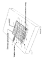
- An example portion of a double-decker detector array 100 is shown in FIG. 1 .
- the detector 100 includes a plurality of detector modules 102 aligned with respect to each other along a substrate 104 in an x-direction 106 .
- Each module 102 includes first and second scintillator rows 108 and 110 optically coupled to corresponding first and second detection regions 112 and 114 of a photodiode substrate 116 .
- the first and second scintillator rows 108 and 110 are arranged with respect to each other such that the first scintillator row 108 is above the second scintillator element 110 with respect to the incoming radiation 120 .
- the first and second scintillator rows 108 and 110 and the detection regions 112 and 114 extend along a z-direction 122 , forming multiple rows of detector elements.
- the resolution of the detector array 100 in the x-direction 106 generally is limited by a finite thickness 124 of the photodiode substrate 116 of each module 102 in the x-direction 106 , which has been on the order of one hundred (100) microns to four hundred (400) microns.
- thinner photodiode substrates are fragile and not well-suited for constructing detector modules such as the detector modules 102 of the detector array 100 .
- a method includes obtaining a photosensor substrate having two opposing major surfaces. One of the two opposing major surfaces includes at least one photosensor row of at least one photosensor element, and the obtained photosensor substrate has a thickness equal to or greater than one hundred microns.
- the method further includes optically coupling a scintillator array to the photosensor substrate.
- the scintillator array includes at least one complementary scintillator row of at least one complementary scintillator element, and the at least one complementary scintillator row is optically coupled to the at least one photosensor row and the at least one complementary scintillator element is optically coupled to the at least one photosensor element.
- the method further includes thinning the photosensor substrate optically coupled to the scintillator producing a thinned photosensor substrate that is optically coupled to the scintillator and that has a thickness on the order of less than one hundred microns.
- an imaging detector includes at least one detector tile including a tile substrate and a plurality of detector modules arranged along an x-direction along the tile substrate.
- a detector module includes a scintillator array having at least one scintillator row of scintillator elements extending along a z-direction coupled to at least one photosensor row of photosensor elements of a photosensor substrate.
- the photosensor substrate is coupled to the scintillator array and has an initial thickness that is equal to or greater than one hundred microns, and the photosensor substrate of the imaging detector has a thinned thickness of less than one hundred microns.
- a method includes assembling an imaging detector module of an imaging system, wherein the imaging detector module includes a scintillator optically coupled to a photosensor substrate, which has a thickness less than one hundred microns.
- the invention may take form in various components and arrangements of components, and in various steps and arrangements of steps.
- the drawings are only for purposes of illustrating the preferred embodiments and are not to be construed as limiting the invention.
- FIG. 1 schematically illustrates a perspective view of a prior art double-decker spectral detector array.
- FIG. 2 schematically illustrates an example imaging system with a spectral detector array including a detector tile with a plurality of detector modules.
- FIG. 3 schematically illustrates a side view of a detector module from the z-direction.
- FIGS. 4-12 illustrate a method for assembling the detector module of FIG. 3 .
- FIG. 13 illustrates an embodiment in which a support carrier is utilized to facilitate making the individual photo-sensor substrates.
- FIG. 2 schematically illustrates an imaging system 200 such as a computed tomography (CT) scanner.
- the imaging system 200 includes a generally stationary gantry portion 202 and a rotating gantry portion 204 .
- the rotating gantry portion 204 is rotatably supported by the generally stationary gantry portion 202 via a bearing (not shown) or the like.
- a radiation source 206 such as an x-ray tube, is supported by the rotating gantry portion 204 and rotates therewith around an examination region 208 about a longitudinal or z-axis 210 in connection with a frame of reference shown at 212 .
- a source collimator 214 collimates radiation emitted by the radiation source 206 , producing a generally cone, fan, wedge or otherwise-shaped radiation beam that traverse the examination region 208 .
- An energy-resolving detector array 218 subtends an angular arc opposite the examination region 208 relative to the radiation source 206 and detects radiation that traverses the examination region 208 .
- the illustrated detector array 218 includes a plurality of tiles 220 .
- Each tile 220 includes a plurality of detector modules 222 1 , . . . , 222 N (wherein N is an integer), arranged on a tile substrate 242 , with respect to each other, along the x-direction.
- the plurality of detector modules 222 1 , . . . , 222 N are also referred to herein as detector modules 222 .
- Each detector module 222 includes a plurality of rows 224 1 , . . . , 224 M (wherein M is an integer equal to or greater than one, and collectively referred to as 224 ) of scintillator elements 226 1 , . . . , 226 K and 228 1 , . . . , 228 K (wherein K is an integer, and collectively referred to as 226 and 228 ) extending along the z-direction.
- M 2
- the detector module is a spectral detector module.
- the rows of scintillator elements 226 and 228 are optically coupled to a corresponding plurality of rows 230 1 , . . .
- 230 M (collectively referred to as 230 ) of photosensor elements 232 1 , . . . , and 234 1 , . . . (collectively referred to as 232 and 234 ) of a photosensor substrate 236 extending along the z-direction.
- Each detector module 222 also includes electrically conductive pathways or pins 238 . Where the detector module 222 further includes processing electronics 240 incorporated into the photosensor substrate 236 (as shown), the electrically conductive pathways or pins 238 are used to route power and digital signals from the processing electronics 240 to the tile substrate 242 . Where the processing electronics 240 are located external to the photosensor substrate 236 , the electrically conductive pathways or pins 238 are used to route signals from the photosensor elements 232 and 234 to the tile substrate 242
- the photosensor substrate 236 in one instance, has an x-axis thickness of less than one hundred (100) microns.
- the detector array 218 can include more detector modules 222 for a given x-axis length relative to a configuration of the detector array with a thicker photosensor substrate (i.e., greater than 100 microns), and hence provide higher resolution in the x-direction.
- such a detector array may include thirty (30) to sixty (60) percent more detector modules 222 .
- Such a detector array may be considered a high definition detector array.
- a reconstructor 246 reconstructs the signals generated by the detector array 218 and generates volumetric image data indicative of the examination region 208 .
- the data from the different rows 230 of photosensor elements 232 and 234 can be individually processed for spectral information and/or combined (e.g., by summing the outputs of the different elements in the same ray path) to produce conventional non-spectral CT data.
- a subject support 248 is configured to position the object or subject in the x, y, and/or z directions with respect to the examination region 208 before, during and/or after scanning the object or the subject.
- a general purpose computing system serves as an operator console 250 , and includes an output device such as a display, an input device such as a keyboard, mouse, and/or the like, one or more processor and computer readable storage medium (e.g., physical memory).
- the console 250 allows the operator to control operation of the system 200 , for example, allowing the operator to select a spectral imaging protocol and/or spectral imaging reconstruction algorithm, initiate scanning, etc.
- FIG. 3 schematically illustrates a side view of a detector module 222 from the z-axis direction.
- the detector module 222 is shown as having two scintillator rows 224 1 and 224 2 and two corresponding photosensor rows 230 1 and 230 2 .
- the detector module 222 may have one or more of each of the scintillator rows 224 and the photosensor rows 224 .
- the detector module 222 includes the photosensor substrate 236 .
- the illustrated photosensor substrate 236 has a thickness 300 on the order of fifty (50) microns (plus or minus a predetermined tolerance), such as a thickness value from a range of ten (10) to ninety (90) microns, twenty-five (25) to seventy-five (75) microns, forty (40) to sixty (60) microns, and/or other thickness value in one or more other ranges.
- a suitable material of the photosensor substrate 236 includes, but is not limited to silicon.
- the photosensor substrate 236 includes a first major surface 302 , with a first region 304 and a second region 306 , and a second opposing major surface 308 .
- the photosensor rows 230 1 and 230 2 are located in the first region 304 of the first major surface 302 .
- the photosensor row 230 1 is an upper row, which is closer to the radiation source 206 ( FIG. 1 ) and hence the incoming radiation
- the photosensor row 230 2 is a lower row, which is farther from the radiation source 206 ( FIG. 1 ) and hence the incoming radiation.
- the scintillator row 224 1 is an upper scintillator element, which is closer to the radiation source 206 ( FIG. 1 ) and hence the incoming radiation
- the scintillator row 224 2 is a lower row, which is farther from the radiation source 206 ( FIG. 1 ) and hence the incoming radiation.
- the upper scintillator row 224 1 is optically coupled to the corresponding upper photosensor row 230 1
- the lower scintillator row 224 2 is optically coupled to the corresponding lower photosensor row 230 2 .
- the upper and lower scintillator row 224 1 and 224 2 are rectangular shaped and are about equal in size. However, it is to be understood that other shapes and different sized scintillator row 224 1 and 224 2 are contemplated herein. Furthermore, spacing between the scintillator row 224 1 and 224 2 can be smaller or larger. Moreover, as the depths (and material) of the scintillator rows 224 can influence energy separation and/or x-ray statistics, the depths, generally, are such that the upper scintillator row 224 1 is primarily responsive to lower energy photons and the lower scintillator row 224 2 is primarily responsive to higher energy photons.
- the photosensor substrate 236 optionally includes the processing electronics 240 (for processing signals from the photosensor elements 232 and 234 ) that are part of the photosensor substrate 236 . As such, there will be fewer electrical pathways from the photosensor substrate 236 to the tile substrate 242 , and z-axis widths of the photosensor elements 232 and 234 can be narrowed, increasing detector resolution in the z-direction.
- processing electronics 240 for processing signals from the photosensor elements 232 and 234
- z-axis widths of the photosensor elements 232 and 234 can be narrowed, increasing detector resolution in the z-direction.
- a non-limiting example of a photosensor substrate with processing electronics incorporated therein is described in patent application PCT/IB2009/054818, filed Oct. 29, 2009, and entitled “Spectral Imaging Detector” (WO/2010/058309), which is incorporated herein by reference in its entirety.
- the sides of the scintillator rows 224 not affixed to the substrate 236 are surrounded by reflective material 312 , which extends over the entire first major surface 302 .
- the combination of the scintillator rows 224 and the reflective material 312 is referred to herein as scintillator array 310 .
- the reflective material 312 can be omitted.
- the reflective material 312 may only cover the first region 304 .
- FIGS. 4-12 describe an approach for assembling the detector array 218 .
- a photosensor substrate having a thickness of greater than one hundred (100) microns is obtained.
- the photosensor substrate 236 is obtained.
- An example of the substrate 236 is schematically illustrated in FIG. 5 and includes the two photosensor rows 232 and 234 , a region 502 for the processing electronics 240 , electrically conductive pads 504 for electrical components, and electrically conductive pads 506 for the electrically conductive pins 238 .
- FIG. 6 schematically shows an embodiment in which the scintillator array 310 to be affixed to the photosensor substrate 236 includes a first surface 602 with a recess 604 and a second surface 606 in the recess 604 for the processing electronics 240 , the electrical components, and the electrically conductive pins 238 .
- various electronics are mounted to the photosensor substrate.
- an integrated chip 702 (including the processing electronics 240 and/or other components) is mounted to the region 502
- electrical components 704 e.g., passive components
- the electrically conductive pins 238 connected to a lead frame 708 are mounted to the electrically conductive pads 506 .
- a scintillator is affixed to the photosensor substrate with the installed electronics, forming a scintillator-photosensor assembly.
- FIG. 8 schematically shows the photosensor substrate 236 with the scintillator array 310 affixed thereto via an optical adhesive, forming a scintillator-photosensor assembly 804 . Note that there are cavities 806 between the electrically conductive pins 238 .
- FIG. 9 schematically shows the scintillator-photosensor assembly 804 with adhesive 902 in cavities 806 between the electrically conductive pins 238 . Note that the lead frame 708 has been removed from the scintillator-photosensor assembly 804 .
- the photosensor substrate is thinned to a thickness of fifty (50) microns or less.
- FIG. 10 schematically shows the scintillator-photosensor assembly 804 with a thinned photosensor substrate 236 having a thickness of fifty (50) microns or less.
- the photosensor substrate 236 can be thinned via grinding. Other thinner techniques are also contemplated herein.
- a detector tile is created from a plurality of the scintillator-photosensor assemblies 804 .
- FIGS. 11 and 12 respectively show bottom and top perspective views in which a plurality of the scintillator-photosensor assemblies 804 are physically and electrically connected to the tile substrate 242 via the pins 238 forming the tile 220 .
- the tile substrate 242 also includes electrically conductive pins 1102 for the physically and electrically connecting the tile 220 to the detector array 218 .
- FIG. 13 illustrates an embodiment in which a support carrier 1302 is utilized to facilitate making the individual substrates 236 .
- a sheet 1304 of material including a plurality of substrates 236 is processed and thinned, for example, to a thickness of less than one hundred microns.
- the sheet 1304 is then transferred to the support carrier 1302 .
- the processing electronics 240 are mounted to the plurality of substrates 236 .
- the individual substrates 236 are then cut from the sheet using a laser, mechanical saw, etc. and left on the carrier 1302 .
- a vacuum chuck feature of the carrier is activated after the individual substrates 236 are cut.
- the scintillator array 310 is then optically coupled to the bonded to the individual substrates 236 and cured.
- the resulting assemblies can then be further processed as described herein.
- processing electronics 240 are located external to the photosensor substrate 236 .
- the module 222 includes a single scintillator row optically couple to a single photosensor row.
- each scintillator row and each photosensor row respectively includes a single scintillator element and a single photosensor element.
Landscapes
- General Physics & Mathematics (AREA)
- Physics & Mathematics (AREA)
- Spectroscopy & Molecular Physics (AREA)
- Life Sciences & Earth Sciences (AREA)
- High Energy & Nuclear Physics (AREA)
- Molecular Biology (AREA)
- Health & Medical Sciences (AREA)
- Condensed Matter Physics & Semiconductors (AREA)
- Electromagnetism (AREA)
- Engineering & Computer Science (AREA)
- Computer Hardware Design (AREA)
- Microelectronics & Electronic Packaging (AREA)
- Power Engineering (AREA)
- Measurement Of Radiation (AREA)
- Apparatus For Radiation Diagnosis (AREA)
Priority Applications (1)
| Application Number | Priority Date | Filing Date | Title |
|---|---|---|---|
| US14/006,703 US9281422B2 (en) | 2011-03-24 | 2012-03-19 | Spectral imaging detector |
Applications Claiming Priority (3)
| Application Number | Priority Date | Filing Date | Title |
|---|---|---|---|
| US201161467044P | 2011-03-24 | 2011-03-24 | |
| PCT/IB2012/051300 WO2012127403A2 (en) | 2011-03-24 | 2012-03-19 | Spectral imaging detector |
| US14/006,703 US9281422B2 (en) | 2011-03-24 | 2012-03-19 | Spectral imaging detector |
Related Parent Applications (1)
| Application Number | Title | Priority Date | Filing Date |
|---|---|---|---|
| PCT/IB2012/051300 A-371-Of-International WO2012127403A2 (en) | 2011-03-24 | 2012-03-19 | Spectral imaging detector |
Related Child Applications (1)
| Application Number | Title | Priority Date | Filing Date |
|---|---|---|---|
| US15/014,297 Division US9599725B2 (en) | 2011-03-24 | 2016-02-03 | Spectral imaging detector |
Publications (2)
| Publication Number | Publication Date |
|---|---|
| US20140015081A1 US20140015081A1 (en) | 2014-01-16 |
| US9281422B2 true US9281422B2 (en) | 2016-03-08 |
Family
ID=45937487
Family Applications (2)
| Application Number | Title | Priority Date | Filing Date |
|---|---|---|---|
| US14/006,703 Active US9281422B2 (en) | 2011-03-24 | 2012-03-19 | Spectral imaging detector |
| US15/014,297 Active US9599725B2 (en) | 2011-03-24 | 2016-02-03 | Spectral imaging detector |
Family Applications After (1)
| Application Number | Title | Priority Date | Filing Date |
|---|---|---|---|
| US15/014,297 Active US9599725B2 (en) | 2011-03-24 | 2016-02-03 | Spectral imaging detector |
Country Status (6)
| Country | Link |
|---|---|
| US (2) | US9281422B2 (ja) |
| EP (1) | EP2689269B1 (ja) |
| JP (1) | JP6071077B2 (ja) |
| CN (1) | CN103443652B (ja) |
| RU (1) | RU2595795C2 (ja) |
| WO (1) | WO2012127403A2 (ja) |
Families Citing this family (17)
| Publication number | Priority date | Publication date | Assignee | Title |
|---|---|---|---|---|
| EP2997397B1 (en) | 2013-05-16 | 2017-10-04 | Koninklijke Philips N.V. | Imaging detector |
| CN105723243B (zh) | 2013-11-15 | 2019-07-09 | 皇家飞利浦有限公司 | 柔性基底上的双面有机光探测器 |
| EP3120383B1 (en) * | 2015-01-15 | 2017-11-29 | Koninklijke Philips N.V. | Imaging detector module assembly |
| EP3532872B1 (en) * | 2016-10-26 | 2024-05-01 | Koninklijke Philips N.V. | Radiation detector scintillator with an integral through-hole interconnect |
| US10247007B2 (en) | 2017-05-02 | 2019-04-02 | General Electric Company | Airfoil shape for a turbine rotor blade |
| US10352170B2 (en) | 2017-05-02 | 2019-07-16 | General Electric Company | Airfoil shape for a turbine rotor blade |
| US10422227B2 (en) | 2017-05-02 | 2019-09-24 | General Electric Company | Airfoil shape for a turbine rotor blade |
| US10280774B2 (en) | 2017-05-03 | 2019-05-07 | General Electric Company | Turbine nozzle airfoil profile |
| US10415406B2 (en) | 2017-05-03 | 2019-09-17 | General Electric Company | Turbine nozzle airfoil profile |
| US10408072B2 (en) | 2017-05-08 | 2019-09-10 | General Electric Company | Turbine nozzle airfoil profile |
| US10436034B2 (en) | 2017-05-15 | 2019-10-08 | General Electric Company | Airfoil shape for a turbine rotor blade |
| US10533440B2 (en) | 2017-05-15 | 2020-01-14 | General Electric Company | Turbine nozzle airfoil profile |
| WO2019041172A1 (en) | 2017-08-30 | 2019-03-07 | Shenzhen United Imaging Healthcare Co., Ltd. | SYSTEM, METHOD AND DETECTOR MODULE FOR PET IMAGING |
| CN111133338A (zh) * | 2017-08-31 | 2020-05-08 | 皇家飞利浦有限公司 | 具有单片闪烁体的多层探测器 |
| DE102018200845B4 (de) | 2018-01-19 | 2021-05-06 | Siemens Healthcare Gmbh | Montageverfahren für die Herstellung eines Röntgendetektors, Röntgendetektor und Röntgengerät |
| US20200185450A1 (en) * | 2018-12-06 | 2020-06-11 | Analog Devices, Inc. | Shielded integrated device packages |
| IT201900010638A1 (it) * | 2019-07-02 | 2021-01-02 | St Microelectronics Srl | Rilevatore di radiazione a scintillatore e dosimetro corrispondente |
Citations (31)
| Publication number | Priority date | Publication date | Assignee | Title |
|---|---|---|---|---|
| US6362480B1 (en) * | 1998-09-10 | 2002-03-26 | Siemens Aktiengesellschaft | Radiation detector, particularly for a computed tomography apparatus |
| US20020163993A1 (en) * | 2000-12-29 | 2002-11-07 | Hoffman David M. | High density flex interconnect for CT detectors |
| US6510195B1 (en) * | 2001-07-18 | 2003-01-21 | Koninklijke Philips Electronics, N.V. | Solid state x-radiation detector modules and mosaics thereof, and an imaging method and apparatus employing the same |
| US20030169847A1 (en) * | 2001-11-21 | 2003-09-11 | University Of Massachusetts Medical Center | System and method for x-ray fluoroscopic imaging |
| US20050072931A1 (en) * | 2003-10-06 | 2005-04-07 | General Electric Company | Solid-state radiation imager with back-side irradiation |
| US20050167603A1 (en) | 2004-01-29 | 2005-08-04 | Ge Medical Systems Global Technology Company, Llc | Apparatus for detecting ionizing radiation |
| US20070057192A1 (en) * | 2003-12-09 | 2007-03-15 | Koninklijke Philips Electronics Nv | Shielding for an x-ray detector |
| US20070085088A1 (en) * | 2001-04-11 | 2007-04-19 | Nihon Kessho Kogaku Co., Ltd. | Component of a radiation detector comprising a substrate with positioning structure for a photoelectric element array |
| US20070235654A1 (en) * | 2004-11-22 | 2007-10-11 | Ge Medical Systems Global Technology Company, Llc | X-ray radiation detector, x-ray imaging apparatus, x-ray ct apparatus and method of manufacturing x-ray detector |
| US20080067392A1 (en) | 2004-08-20 | 2008-03-20 | Kazuhisa Miyaguchi | Radiation Imaging Device and Radiation Imaging Method |
| US20080203309A1 (en) * | 2005-04-22 | 2008-08-28 | Koninklijke Philips Electronics N.V. | Digital silicon photomultiplier for TOF-PET |
| US20080210877A1 (en) | 2005-04-26 | 2008-09-04 | Koninklijke Philips Electronics N. V. | Double Decker Detector For Spectral Ct |
| US20080253507A1 (en) * | 2005-10-05 | 2008-10-16 | Koninklijke Philips Electronics N. V. | Computed Tomography Detector Using Thin Circuits |
| US20090121146A1 (en) * | 2006-03-30 | 2009-05-14 | Koninklijke Philips Electronics N. V. | Radiation detector array |
| US20090140156A1 (en) * | 2004-10-28 | 2009-06-04 | Siemens Aktiengesellschaft | Radiation Detector for Detecting Radiation |
| US20090152447A1 (en) * | 2007-12-17 | 2009-06-18 | Nihon Kessho Kogaku Co., Ltd. | Photo Detector and Photo Detection Apparatus Provided with Photo Detector |
| US20090181491A1 (en) * | 2006-11-24 | 2009-07-16 | Tower Semiconductor Ltd. | High-Resolution Integrated X-Ray CMOS Image Sensor |
| US7692156B1 (en) * | 2006-08-23 | 2010-04-06 | Radiation Monitoring Devices, Inc. | Beam-oriented pixellated scintillators for radiation imaging |
| WO2010058309A2 (en) | 2008-11-18 | 2010-05-27 | Koninklijke Philips Electronics N.V. | Spectral imaging detector |
| US20100155606A1 (en) * | 2008-12-19 | 2010-06-24 | Samsung Electronics Co., Ltd. | Method and apparatus for acquiring images created by penetration of radioactive ray |
| US20100200760A1 (en) * | 2009-02-06 | 2010-08-12 | Koninklijke Philips Electronics N.V. | Radiation detector with a stack of scintillator elements and photodiode arrays |
| US20100220833A1 (en) | 2005-04-26 | 2010-09-02 | Koninklijke Philips Electronics N. V. | Detector array for spectral ct |
| US20100264322A1 (en) | 2007-12-21 | 2010-10-21 | Koninklijke Philips Electronics N.V. | Radiation-sensitive detector with a scintillator in a composite resin |
| US20100276600A1 (en) * | 2007-11-09 | 2010-11-04 | Koninklijke Philips Electronics N.V. | Protection of hygroscopic scintillators |
| US20100308227A1 (en) * | 2008-02-04 | 2010-12-09 | Hiromichi Tonami | Radiation detector and tomography equipment provided with the same |
| US20110056618A1 (en) * | 2008-06-05 | 2011-03-10 | Hiromichi Tonami | Method of manufacturing radiation detector |
| US20110113611A1 (en) * | 2008-07-22 | 2011-05-19 | Hiromichi Tonami | Method of manufacturing radiation tomography apparatus |
| EP2404249A1 (en) | 2009-03-05 | 2012-01-11 | SanDisk IL Ltd. | System for optimizing the transfer of stored content in response to a triggering event |
| US20120193540A1 (en) * | 2011-01-31 | 2012-08-02 | Fujifilm Corporation | Radiological image detection apparatus and method for manufacturing the same |
| US20130248723A1 (en) * | 2010-07-30 | 2013-09-26 | Varian Medical Systems, Inc. | Radiation detector with multiple operating schemes |
| US8586933B2 (en) * | 2007-04-25 | 2013-11-19 | Koninklijke Philips N.V. | Radiation detector having a split laminate optical coupling |
Family Cites Families (13)
| Publication number | Priority date | Publication date | Assignee | Title |
|---|---|---|---|---|
| JPS57172272A (en) * | 1981-04-17 | 1982-10-23 | Toshiba Corp | Multichannel type radiation detector |
| US5043582A (en) * | 1985-12-11 | 1991-08-27 | General Imagining Corporation | X-ray imaging system and solid state detector therefor |
| JPS62231222A (ja) | 1986-03-31 | 1987-10-09 | Nitto Electric Ind Co Ltd | 液晶配向膜形成用溶液 |
| US5179284A (en) * | 1991-08-21 | 1993-01-12 | General Electric Company | Solid state radiation imager having a reflective and protective coating |
| RU2123710C1 (ru) * | 1996-01-31 | 1998-12-20 | Товарищество с ограниченной ответственностью "Медтех" | Матричный рентгеновский приемник |
| FR2758630B1 (fr) * | 1997-01-21 | 1999-04-09 | Thomson Tubes Electroniques | Procede de scellement etanche d'un detecteur de rayonnement a l'etat solide et detecteur obtenu par ce procede |
| US6114703A (en) * | 1997-10-21 | 2000-09-05 | The Regents Of The University Of California | High resolution scintillation detector with semiconductor readout |
| JP5038209B2 (ja) * | 2001-04-11 | 2012-10-03 | 日本結晶光学株式会社 | 放射線検出装置 |
| AU2003250429A1 (en) * | 2002-09-18 | 2004-04-08 | Koninklijke Philips Electronics N.V. | Radiation detector |
| US7399972B2 (en) * | 2005-06-09 | 2008-07-15 | Nihon Kessho Kogaku Co., Ltd. | Component for radiation detector and radiation detector |
| US7737409B2 (en) * | 2008-06-12 | 2010-06-15 | Analog Devices, Inc. | Silicon detector and method for constructing silicon detectors |
| CN102216807B (zh) * | 2008-11-21 | 2016-08-17 | 皇家飞利浦电子股份有限公司 | 平铺式辐射检测器的组装方法 |
| JP5247486B2 (ja) * | 2009-01-16 | 2013-07-24 | 浜松ホトニクス株式会社 | 裏面入射型フォトダイオードアレイ及び放射線検出器 |
-
2012
- 2012-03-19 RU RU2013147397/28A patent/RU2595795C2/ru not_active IP Right Cessation
- 2012-03-19 JP JP2014500514A patent/JP6071077B2/ja active Active
- 2012-03-19 EP EP20120713356 patent/EP2689269B1/en active Active
- 2012-03-19 US US14/006,703 patent/US9281422B2/en active Active
- 2012-03-19 CN CN201280014657.2A patent/CN103443652B/zh active Active
- 2012-03-19 WO PCT/IB2012/051300 patent/WO2012127403A2/en active Application Filing
-
2016
- 2016-02-03 US US15/014,297 patent/US9599725B2/en active Active
Patent Citations (32)
| Publication number | Priority date | Publication date | Assignee | Title |
|---|---|---|---|---|
| US6362480B1 (en) * | 1998-09-10 | 2002-03-26 | Siemens Aktiengesellschaft | Radiation detector, particularly for a computed tomography apparatus |
| US20020163993A1 (en) * | 2000-12-29 | 2002-11-07 | Hoffman David M. | High density flex interconnect for CT detectors |
| US20070085088A1 (en) * | 2001-04-11 | 2007-04-19 | Nihon Kessho Kogaku Co., Ltd. | Component of a radiation detector comprising a substrate with positioning structure for a photoelectric element array |
| US6510195B1 (en) * | 2001-07-18 | 2003-01-21 | Koninklijke Philips Electronics, N.V. | Solid state x-radiation detector modules and mosaics thereof, and an imaging method and apparatus employing the same |
| US20030169847A1 (en) * | 2001-11-21 | 2003-09-11 | University Of Massachusetts Medical Center | System and method for x-ray fluoroscopic imaging |
| US20050072931A1 (en) * | 2003-10-06 | 2005-04-07 | General Electric Company | Solid-state radiation imager with back-side irradiation |
| US20070057192A1 (en) * | 2003-12-09 | 2007-03-15 | Koninklijke Philips Electronics Nv | Shielding for an x-ray detector |
| US20050167603A1 (en) | 2004-01-29 | 2005-08-04 | Ge Medical Systems Global Technology Company, Llc | Apparatus for detecting ionizing radiation |
| US20080067392A1 (en) | 2004-08-20 | 2008-03-20 | Kazuhisa Miyaguchi | Radiation Imaging Device and Radiation Imaging Method |
| US20090140156A1 (en) * | 2004-10-28 | 2009-06-04 | Siemens Aktiengesellschaft | Radiation Detector for Detecting Radiation |
| US20070235654A1 (en) * | 2004-11-22 | 2007-10-11 | Ge Medical Systems Global Technology Company, Llc | X-ray radiation detector, x-ray imaging apparatus, x-ray ct apparatus and method of manufacturing x-ray detector |
| US20080203309A1 (en) * | 2005-04-22 | 2008-08-28 | Koninklijke Philips Electronics N.V. | Digital silicon photomultiplier for TOF-PET |
| US20080210877A1 (en) | 2005-04-26 | 2008-09-04 | Koninklijke Philips Electronics N. V. | Double Decker Detector For Spectral Ct |
| US20100220833A1 (en) | 2005-04-26 | 2010-09-02 | Koninklijke Philips Electronics N. V. | Detector array for spectral ct |
| US20080253507A1 (en) * | 2005-10-05 | 2008-10-16 | Koninklijke Philips Electronics N. V. | Computed Tomography Detector Using Thin Circuits |
| US20090121146A1 (en) * | 2006-03-30 | 2009-05-14 | Koninklijke Philips Electronics N. V. | Radiation detector array |
| US7692156B1 (en) * | 2006-08-23 | 2010-04-06 | Radiation Monitoring Devices, Inc. | Beam-oriented pixellated scintillators for radiation imaging |
| US20090181491A1 (en) * | 2006-11-24 | 2009-07-16 | Tower Semiconductor Ltd. | High-Resolution Integrated X-Ray CMOS Image Sensor |
| US8586933B2 (en) * | 2007-04-25 | 2013-11-19 | Koninklijke Philips N.V. | Radiation detector having a split laminate optical coupling |
| US20100276600A1 (en) * | 2007-11-09 | 2010-11-04 | Koninklijke Philips Electronics N.V. | Protection of hygroscopic scintillators |
| US20090152447A1 (en) * | 2007-12-17 | 2009-06-18 | Nihon Kessho Kogaku Co., Ltd. | Photo Detector and Photo Detection Apparatus Provided with Photo Detector |
| US20100264322A1 (en) | 2007-12-21 | 2010-10-21 | Koninklijke Philips Electronics N.V. | Radiation-sensitive detector with a scintillator in a composite resin |
| US20100308227A1 (en) * | 2008-02-04 | 2010-12-09 | Hiromichi Tonami | Radiation detector and tomography equipment provided with the same |
| US20110056618A1 (en) * | 2008-06-05 | 2011-03-10 | Hiromichi Tonami | Method of manufacturing radiation detector |
| US20110113611A1 (en) * | 2008-07-22 | 2011-05-19 | Hiromichi Tonami | Method of manufacturing radiation tomography apparatus |
| WO2010058309A2 (en) | 2008-11-18 | 2010-05-27 | Koninklijke Philips Electronics N.V. | Spectral imaging detector |
| US20110210256A1 (en) * | 2008-11-18 | 2011-09-01 | Koninklijke Philips Electronics N.V. | Spectral imaging detector |
| US20100155606A1 (en) * | 2008-12-19 | 2010-06-24 | Samsung Electronics Co., Ltd. | Method and apparatus for acquiring images created by penetration of radioactive ray |
| US20100200760A1 (en) * | 2009-02-06 | 2010-08-12 | Koninklijke Philips Electronics N.V. | Radiation detector with a stack of scintillator elements and photodiode arrays |
| EP2404249A1 (en) | 2009-03-05 | 2012-01-11 | SanDisk IL Ltd. | System for optimizing the transfer of stored content in response to a triggering event |
| US20130248723A1 (en) * | 2010-07-30 | 2013-09-26 | Varian Medical Systems, Inc. | Radiation detector with multiple operating schemes |
| US20120193540A1 (en) * | 2011-01-31 | 2012-08-02 | Fujifilm Corporation | Radiological image detection apparatus and method for manufacturing the same |
Also Published As
| Publication number | Publication date |
|---|---|
| US9599725B2 (en) | 2017-03-21 |
| WO2012127403A3 (en) | 2012-12-27 |
| US20160154121A1 (en) | 2016-06-02 |
| JP6071077B2 (ja) | 2017-02-01 |
| WO2012127403A2 (en) | 2012-09-27 |
| JP2014513279A (ja) | 2014-05-29 |
| CN103443652B (zh) | 2017-02-15 |
| RU2595795C2 (ru) | 2016-08-27 |
| US20140015081A1 (en) | 2014-01-16 |
| RU2013147397A (ru) | 2015-04-27 |
| EP2689269B1 (en) | 2015-05-13 |
| EP2689269A2 (en) | 2014-01-29 |
| CN103443652A (zh) | 2013-12-11 |
Similar Documents
| Publication | Publication Date | Title |
|---|---|---|
| US9599725B2 (en) | Spectral imaging detector | |
| US9012857B2 (en) | Multi-layer horizontal computed tomography (CT) detector array with at least one thin photosensor array layer disposed between at least two scintillator array layers | |
| US20080253507A1 (en) | Computed Tomography Detector Using Thin Circuits | |
| JP5455620B2 (ja) | 放射線検出器および当該検出器を含む装置 | |
| NL2008201C2 (en) | Detector systems with anode incidence face and methods of fabricating the same. | |
| RU2647206C1 (ru) | Сенсорное устройство и система визуализации для обнаружения сигналов излучения | |
| US9638810B2 (en) | Imaging detector | |
| US8525119B2 (en) | Detector array with pre-focused anti-scatter grid | |
| JP6816129B2 (ja) | モジュール式x線検出器 | |
| JP6194126B2 (ja) | モジュライメージング検出器asic | |
| US20210278553A1 (en) | Three-dimensional solid state imaging photodetector | |
| JP7034635B2 (ja) | 検出器モジュール、放射線検出器、x線コンピュータ断層撮影装置及び放射線検出器の製造方法 |
Legal Events
| Date | Code | Title | Description |
|---|---|---|---|
| AS | Assignment |
Owner name: KONINKLIJKE PHILIPS ELECTRONICS N V, NETHERLANDS Free format text: ASSIGNMENT OF ASSIGNORS INTEREST;ASSIGNORS:LUHTA, RANDALL PETER;MATTSON, RODNEY ARNOLD;SIGNING DATES FROM 20110314 TO 20110324;REEL/FRAME:031255/0942 |
|
| STCF | Information on status: patent grant |
Free format text: PATENTED CASE |
|
| MAFP | Maintenance fee payment |
Free format text: PAYMENT OF MAINTENANCE FEE, 4TH YEAR, LARGE ENTITY (ORIGINAL EVENT CODE: M1551); ENTITY STATUS OF PATENT OWNER: LARGE ENTITY Year of fee payment: 4 |
|
| MAFP | Maintenance fee payment |
Free format text: PAYMENT OF MAINTENANCE FEE, 8TH YEAR, LARGE ENTITY (ORIGINAL EVENT CODE: M1552); ENTITY STATUS OF PATENT OWNER: LARGE ENTITY Year of fee payment: 8 |