US9274416B2 - Method for forming photo-mask and OPC method - Google Patents

Method for forming photo-mask and OPC method Download PDF

Info

Publication number
US9274416B2
US9274416B2 US14/023,476 US201314023476A US9274416B2 US 9274416 B2 US9274416 B2 US 9274416B2 US 201314023476 A US201314023476 A US 201314023476A US 9274416 B2 US9274416 B2 US 9274416B2
Authority
US
United States
Prior art keywords
photo
mask pattern
mask
opc
line
Prior art date
Legal status (The legal status is an assumption and is not a legal conclusion. Google has not performed a legal analysis and makes no representation as to the accuracy of the status listed.)
Active, expires
Application number
US14/023,476
Other versions
US20150072272A1 (en
Inventor
Chun-Hsien Huang
Ming-Jui Chen
Chia-Wei Huang
Hsin-Yu Chen
Kai-Lin Chuang
Current Assignee (The listed assignees may be inaccurate. Google has not performed a legal analysis and makes no representation or warranty as to the accuracy of the list.)
United Microelectronics Corp
Original Assignee
United Microelectronics Corp
Priority date (The priority date is an assumption and is not a legal conclusion. Google has not performed a legal analysis and makes no representation as to the accuracy of the date listed.)
Filing date
Publication date
Application filed by United Microelectronics Corp filed Critical United Microelectronics Corp
Priority to US14/023,476 priority Critical patent/US9274416B2/en
Assigned to UNITED MICROELECTRONICS CORP. reassignment UNITED MICROELECTRONICS CORP. ASSIGNMENT OF ASSIGNORS INTEREST (SEE DOCUMENT FOR DETAILS). Assignors: CHEN, HSIN-YU, CHEN, MING-JUI, CHUANG, KAI-LIN, HUANG, CHIA-WEI, HUANG, CHUN-HSIEN
Publication of US20150072272A1 publication Critical patent/US20150072272A1/en
Application granted granted Critical
Publication of US9274416B2 publication Critical patent/US9274416B2/en
Active legal-status Critical Current
Adjusted expiration legal-status Critical

Links

Images

Classifications

    • GPHYSICS
    • G03PHOTOGRAPHY; CINEMATOGRAPHY; ANALOGOUS TECHNIQUES USING WAVES OTHER THAN OPTICAL WAVES; ELECTROGRAPHY; HOLOGRAPHY
    • G03FPHOTOMECHANICAL PRODUCTION OF TEXTURED OR PATTERNED SURFACES, e.g. FOR PRINTING, FOR PROCESSING OF SEMICONDUCTOR DEVICES; MATERIALS THEREFOR; ORIGINALS THEREFOR; APPARATUS SPECIALLY ADAPTED THEREFOR
    • G03F1/00Originals for photomechanical production of textured or patterned surfaces, e.g., masks, photo-masks, reticles; Mask blanks or pellicles therefor; Containers specially adapted therefor; Preparation thereof
    • G03F1/36Masks having proximity correction features; Preparation thereof, e.g. optical proximity correction [OPC] design processes
    • GPHYSICS
    • G03PHOTOGRAPHY; CINEMATOGRAPHY; ANALOGOUS TECHNIQUES USING WAVES OTHER THAN OPTICAL WAVES; ELECTROGRAPHY; HOLOGRAPHY
    • G03FPHOTOMECHANICAL PRODUCTION OF TEXTURED OR PATTERNED SURFACES, e.g. FOR PRINTING, FOR PROCESSING OF SEMICONDUCTOR DEVICES; MATERIALS THEREFOR; ORIGINALS THEREFOR; APPARATUS SPECIALLY ADAPTED THEREFOR
    • G03F1/00Originals for photomechanical production of textured or patterned surfaces, e.g., masks, photo-masks, reticles; Mask blanks or pellicles therefor; Containers specially adapted therefor; Preparation thereof
    • G03F1/68Preparation processes not covered by groups G03F1/20 - G03F1/50
    • G03F1/72Repair or correction of mask defects
    • G03F1/144

Definitions

  • the present invention relates to an OPC method and method using the OPC method for forming at least a photo-mask, and more particularly, the photo-masks are used in a self aligned via (SAV) process.
  • SAV self aligned via
  • the integrated circuit layout is first designed and formed as a photo-mask pattern.
  • the photo-mask pattern is then proportionally transferred to a photoresist layer positioned on the semiconductor wafer.
  • the design rule of line width and space between lines or devices becomes finer.
  • the width is subject to optical characteristics.
  • the interval between transparent regions in a mask is scaled down with device size.
  • the light passes through the mask, diffraction occurs and reduces resolution.
  • the light through the regions having small interval sizes is influenced by the transparent regions having large interval sizes and results in deformation of the transfer pattern.
  • OPC optical proximity correction
  • the “dual damascene” process is widely used to form a metal interconnection system which is consisted of metal lines and plugs.
  • the OPC method used for forming the masks of the metal interconnection system is not well studied.
  • the present invention therefore provides a method for forming at least a photo-mask, which can be used in a dual-damascene process, especially a SAV process.
  • a method for forming a photo-mask is provided.
  • a first photo-mask pattern relating to a first line, an original second photo-mask pattern relating to a first via plug, and a third photo-mask pattern relating to a second line are provided.
  • the first line, the first via plug and the second line are disposed in sequence in a semiconductor structure, and the first via plug is disposed at the intersection of the first line and the second line.
  • a first optical proximity correction (OPC) process is performed, comprising a comparing step and/or a modification step for the original second photo-mask pattern.
  • a second OPC process is performed, comprising enlarging a width of the second photo-mask pattern along the first direction.
  • a revised second photo-resist pattern is formed.
  • a contour simulation process is performed to make sure the revised second photo-mask pattern is larger or equal to the original second-mask pattern.
  • the first photo-mask pattern is output to form a first photo-mask
  • the revised second photo-mask pattern is output to form a second photo-mask
  • the third photo-mask pattern is output to form a third photo-mask.
  • an OPC process is provided.
  • a first photo-mask pattern relating to a first line, an original second photo-mask pattern relating to a first via plug, and a third photo-mask pattern relating to a second line are provided.
  • the first line, the first via plug and the second line are disposed in sequence in a semiconductor structure, and the first via plug is disposed at the intersection of the first line and the second line.
  • a first optical proximity correction (OPC) process is performed, comprising a comparing step and/or a modification step for the original second photo-mask pattern.
  • a second OPC process is performed, comprising enlarging a width of the second photo-mask pattern along the first direction.
  • a revised second photo-resist pattern is formed.
  • a contour simulation process is performed to make sure the revised second photo-mask pattern is larger or equal to the original second-mask pattern.
  • the method is characterized in that the second OPC process is performed to enlarge the width of the second photo-mask pattern along the first direction. Since it is specially applied to the SAV process, the second photo-mask with enlarged width can gain more process window but does not affect the formed area of the first via plug.
  • FIG. 1 to FIG. 7 show schematic diagrams of the semiconductor structure in the present invention.
  • FIG. 8 shows a flow chart of the method for forming a photo-resist in the present invention.
  • FIG. 9 to FIG. 13 show schematic diagrams of the layout of the first photo-mask, the second photo-mask, and the third photo-mask in the present invention.
  • the present invention is related to a method for forming photo-masks which is used in a semiconductor process to form a semiconductor structure.
  • the semiconductor process is a metal dual damascene process
  • the semiconductor structure is a metal interconnection system, but is not limited thereto.
  • FIG. 1 and FIG. 7 show schematic diagrams of the semiconductor structure in the present invention, wherein FIG. 1 shows a top view and FIG. 7 shows a three dimensional view. As shown in FIG. 1 and FIG.
  • the semiconductor structure to be formed in the present invention for example, includes a first metal line 304 , a first via plug 314 and a second metal line 312 , which are disposed in a first dielectric layer 302 and a second dielectric layer 306 .
  • the first metal line 304 extends along a first direction 400
  • the second metal line 312 extends along a second direction 402 .
  • the first direction 400 and the second direction 402 is substantially perpendicular to each other, but is not limited thereto. It is noted that the numbering only shows the relative position but does not indicate the real stacking position on the substrate.
  • the semiconductor device shown in FIG. 1 and FIG. 7 is fabricated by a “self aligned via (SAV) process” which includes using a first photo- mask (not shown) corresponding to the first metal line 304 , a second photo-mask (not shown) corresponding to the first via plug 314 , and a third photo-mask (not shown) corresponding to the second metal line 312 .
  • SAV self aligned via
  • FIG. 2 to FIG. 7 show three dimensional schematic diagrams of the method for forming a semiconductor structure in the present invention.
  • a substrate 300 is provided.
  • the substrate 300 may be a silicon substrate or a dielectric layer on the silicon substrate, but is not limited thereto.
  • a first dielectric layer 302 is formed on the substrate 300 .
  • the first metal line 304 stretching along the first direction 400 is formed in the first dielectric layer 302 .
  • the step of forming the first metal line 304 includes forming a photoresist layer (not shown) and then patterning it by using the first photo-mask (not shown), then, an etching process is carried out by using the patterned photoresist layer as a mask to pattern the first dielectric layer 302 , thereby forming a trench (not shown), then filling a metal layer into the trench and performing a planarization process.
  • the first metal line 304 is therefore in the first dielectric layer 302 .
  • a second dielectric layer 306 is formed on the first dielectric layer 302 .
  • the step of forming the trench 308 includes a photo-etching-process (PEP) by using the third photo-mask (not shown) (which may be similar to the steps shown above), so as to form a patterned mask layer 307 .
  • PEP photo-etching-process
  • the trench 308 is formed in the second dielectric layer 306 and is stretching along the second direction 402 .
  • a photoresist layer 309 is formed on the second dielectric layer 306 , filling the trench 308 and covering the patterned mask layer 307 .
  • a lithography process is performed by using a second photo-mask (not shown) to form an opening 311 .
  • the opening 311 therefore exposes the second dielectric layer 306 in the trench 308 .
  • the opening 311 is large than expected (for example, a width of the opening 311 is larger than the width of the trench 308 along the first direction 400 ). But since the second dielectric layer 306 in the trench 308 is not covered by the patterned mask layer 307 , after forming the opening 311 , only the second dielectric layer 306 in the trench 308 is exposed.
  • an etching process is carried out by using the patterned photoresist layer 309 as a mask to etch the second dielectric layer 306 until exposing the first metal line 304 .
  • the patterned mask layer 307 which has an etching selectivity with respect to the second dielectric layer 306 , only the second dielectric layer 306 in the trench 308 is removed, and those outside the trench 308 covered by the patterned mask layer 307 is not removed.
  • the photoresist layer 309 is removed away.
  • a via 313 exposing the first metal line 304 is therefore formed.
  • a metal material is filled into the trench 308 and the via 313 and a planarization process is performed by using the patterned mask layer 307 as a mask.
  • the patterned mask layer 307 can be completely removed or partially removed. Accordingly, the metal material in the trench 308 becomes a second metal line 312 and the metal material in the via 313 becomes the first via plug 314 .
  • the first via plug 314 is therefore referred as a “self aligned via (SAV)” and the method through FIG. 2 to FIG. 7 is referred as a SAV process.
  • SAV self aligned via
  • the present invention further provides a method for forming a first photo-mask, a second photo-mask, and a third photo-mask, wherein the first photo-mask corresponds to the first metal line 304 , the second photo-mask corresponds to the first via plug 314 , and the third photo-mask corresponds to the second metal line 312 .
  • FIG. 8 illustrating a flow chart of the method for forming a photo-resist in the present invention.
  • FIG. 9 to FIG. 13 are schematic diagrams showing the layout of the first photo-mask, the second photo-mask, and the third photo-mask in the present invention.
  • a first photo-mask pattern 304 M, a second photo-mask pattern 314 M and a third photo-mask pattern 312 M are provided.
  • the first photo-mask pattern 304 M is related to the first metal line 304 in FIG. 1
  • the second photo-mask pattern 314 M is related to the first via plug 314 in FIG. 1
  • the third photo-mask pattern 312 M is related to the second metal line 312 in FIG. 1
  • the first photo-mask pattern 304 M extends along a first direction 400 and the third photo-resist mask pattern 312 M extends along a second direction 402 .
  • the second photo-resist mask pattern 314 M is disposed at the intersection of the first photo-mask pattern 304 M and the third photo-mask pattern 312 M.
  • a first optical proximity correction (OPC) process is performed.
  • the first OPC can be any conventional OPC methods that include a comparing step and/or a modification step.
  • the comparing step considers the shape, the area or the relative position of the second photo-mask pattern 314 M according to a rule, and if the second photo-mask pattern 314 M needs to be modified, the modification step will modify the second photo-mask pattern 314 M.
  • the original second photo-mask pattern 314 M becomes a second photo-mask pattern 314 M′, which has a greater area in the present embodiment.
  • the original second photo-mask pattern 314 M is not changed.
  • a second OPC process is performed by enlarging a width of the second photo-mask pattern 314 M′ along the second direction 402 to form a second photo-resist pattern 314 M′′.
  • the first via plug 314 (corresponding to the second photo-mask pattern 314 M) is formed within the trench 308 (corresponding to the third photo-mask pattern 312 M), so enlarging the width of the second photo-mask pattern 314 M′ along the second direction 402 would not affect the formed area of the first via plug 314 .
  • enlarging the width of the second photo-mask pattern 314 M′ can increase the process window so the accuracy of the method can be improved.
  • the enlarging step can be performed by a Boolean process to calculate the value of the enlarging width.
  • the length of the second photo-mask pattern 314 M′ along the first direction 400 can be reduced, so as to maintain the depth of field (DOF) of each via pattern and keep the area around a fixed value.
  • DOF depth of field
  • the sequence of the first OPC process and the second OPC process can be exchanged.
  • the first OPC process is performed before the second OPC process.
  • a contour simulation process is performed to make sure the revised second photo-mask pattern 314 M′′′ is larger or equal to the original second-mask pattern 314 M. If the revised second photo-mask pattern 314 M′′′ is smaller than the original second photo-mask pattern 314 M, another modification process is carried out to enlarge the revised second mask pattern 314 M′′′ until it is not less than the original second mask pattern 314 M.
  • the first photo-mask pattern 304 M is output to form a first photo-mask (not shown)
  • the revised second photo-mask pattern 314 M′′′ is output to form a second photo-mask (not shown)
  • the third photo-mask pattern 312 M is output to form a third photo-mask pattern (not shown).
  • the first photo-mask, the second photo-mask and the third photo-mask pattern can be used in the SAV method, as shown in FIG. 2 to FIG. 7 for example, so as to form the semiconductor device in FIG. 1 and FIG. 7 .
  • the method for forming a photo-mask in the present invention is not limited to the above-mentioned embodiment.
  • the structure to be formed is not limited to the dual damascene structure in FIG. 1 and FIG. 7 , but can be any structure that has an upper line pattern, a lower line pattern and a via pattern disposed therebetween.
  • the upper line pattern can intersect the lower pattern in any angle and the via pattern is located at the intersection.
  • the present invention provides a method for forming a photo-mask.
  • the method is characterized in that the second OPC process is performed to enlarge the width of the second photo-mask pattern along the second direction. Since the method is specially applied to the SAV process, the second photo-mask with enlarged width can gain more process window but does not affect the formed area of the first via plug.

Landscapes

  • Physics & Mathematics (AREA)
  • General Physics & Mathematics (AREA)
  • Exposure And Positioning Against Photoresist Photosensitive Materials (AREA)

Abstract

A method for forming a photo-mask is provided. A first photo-mask pattern relating to a first line, an original second photo-mask pattern relating to a first via plug, and a third photo-mask pattern relating to a second line are provided. A first optical proximity correction (OPC) process is performed. A second OPC process is performed, comprising enlarging a width of the second photo-mask pattern along the first direction to form a revised second photo-resist pattern. A contour simulation process is performed to make sure the revised second photo-mask pattern is larger or equal to the original second-mask pattern. The first photo-mask pattern, the revised second photo-mask pattern, and the third photo-mask pattern are output. The present invention further provides an OPC method.

Description

BACKGROUND OF THE INVENTION
1. Field of the Invention
The present invention relates to an OPC method and method using the OPC method for forming at least a photo-mask, and more particularly, the photo-masks are used in a self aligned via (SAV) process.
2. Description of the Prior Art
In semiconductor manufacturing processes, in order to transfer an integrated circuit layout onto a semiconductor wafer, the integrated circuit layout is first designed and formed as a photo-mask pattern. The photo-mask pattern is then proportionally transferred to a photoresist layer positioned on the semiconductor wafer.
In recent years, with the increasing miniaturization of semiconductor devices, the design rule of line width and space between lines or devices becomes finer. However, the width is subject to optical characteristics. To obtain fine-sized devices in the exposure, the interval between transparent regions in a mask is scaled down with device size. When the light passes through the mask, diffraction occurs and reduces resolution. Moreover, when light passes through the transparent regions of a mask having different interval sizes, the light through the regions having small interval sizes is influenced by the transparent regions having large interval sizes and results in deformation of the transfer pattern. Currently, a technique called “optical proximity correction (OPC)” is developed. The OPC method is used to imitate the feature that light passes through the photo-mask and to further compensate the pattern of the mask to form the desired pattern after the exposure process.
In the conventional arts, the “dual damascene” process is widely used to form a metal interconnection system which is consisted of metal lines and plugs. However, the OPC method used for forming the masks of the metal interconnection system is not well studied.
SUMMARY OF THE INVENTION
The present invention therefore provides a method for forming at least a photo-mask, which can be used in a dual-damascene process, especially a SAV process.
A method for forming a photo-mask is provided. A first photo-mask pattern relating to a first line, an original second photo-mask pattern relating to a first via plug, and a third photo-mask pattern relating to a second line are provided. The first line, the first via plug and the second line are disposed in sequence in a semiconductor structure, and the first via plug is disposed at the intersection of the first line and the second line. A first optical proximity correction (OPC) process is performed, comprising a comparing step and/or a modification step for the original second photo-mask pattern. A second OPC process is performed, comprising enlarging a width of the second photo-mask pattern along the first direction. A revised second photo-resist pattern is formed. A contour simulation process is performed to make sure the revised second photo-mask pattern is larger or equal to the original second-mask pattern. The first photo-mask pattern is output to form a first photo-mask, the revised second photo-mask pattern is output to form a second photo-mask, and the third photo-mask pattern is output to form a third photo-mask.
According to another embodiment, an OPC process is provided. A first photo-mask pattern relating to a first line, an original second photo-mask pattern relating to a first via plug, and a third photo-mask pattern relating to a second line are provided. The first line, the first via plug and the second line are disposed in sequence in a semiconductor structure, and the first via plug is disposed at the intersection of the first line and the second line. A first optical proximity correction (OPC) process is performed, comprising a comparing step and/or a modification step for the original second photo-mask pattern. A second OPC process is performed, comprising enlarging a width of the second photo-mask pattern along the first direction. A revised second photo-resist pattern is formed. A contour simulation process is performed to make sure the revised second photo-mask pattern is larger or equal to the original second-mask pattern.
The method is characterized in that the second OPC process is performed to enlarge the width of the second photo-mask pattern along the first direction. Since it is specially applied to the SAV process, the second photo-mask with enlarged width can gain more process window but does not affect the formed area of the first via plug.
These and other objectives of the present invention will no doubt become obvious to those of ordinary skill in the art after reading the following detailed description of the preferred embodiment that is illustrated in the various figures and drawings.
BRIEF DESCRIPTION OF THE DRAWINGS
FIG. 1 to FIG. 7 show schematic diagrams of the semiconductor structure in the present invention.
FIG. 8 shows a flow chart of the method for forming a photo-resist in the present invention.
FIG. 9 to FIG. 13 show schematic diagrams of the layout of the first photo-mask, the second photo-mask, and the third photo-mask in the present invention.
DETAILED DESCRIPTION
To provide a better understanding of the presented invention, preferred embodiments will be made in detail. The preferred embodiments of the present invention are illustrated in the accompanying drawings with numbered elements.
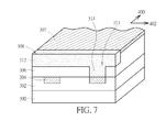
The present invention is related to a method for forming photo-masks which is used in a semiconductor process to form a semiconductor structure. In one embodiment, the semiconductor process is a metal dual damascene process, and the semiconductor structure is a metal interconnection system, but is not limited thereto. Please refer to FIG. 1 and FIG. 7, which show schematic diagrams of the semiconductor structure in the present invention, wherein FIG. 1 shows a top view and FIG. 7 shows a three dimensional view. As shown in FIG. 1 and FIG. 7, the semiconductor structure to be formed in the present invention, for example, includes a first metal line 304, a first via plug 314 and a second metal line 312, which are disposed in a first dielectric layer 302 and a second dielectric layer 306. In one embodiment, the first metal line 304 extends along a first direction 400, and the second metal line 312 extends along a second direction 402. Preferably, the first direction 400 and the second direction 402 is substantially perpendicular to each other, but is not limited thereto. It is noted that the numbering only shows the relative position but does not indicate the real stacking position on the substrate.
In one preferred embodiment, the semiconductor device shown in FIG. 1 and FIG. 7 is fabricated by a “self aligned via (SAV) process” which includes using a first photo- mask (not shown) corresponding to the first metal line 304, a second photo-mask (not shown) corresponding to the first via plug 314, and a third photo-mask (not shown) corresponding to the second metal line 312. For the detail description of the SAV process, please refer to FIG. 2 to FIG. 7, which show three dimensional schematic diagrams of the method for forming a semiconductor structure in the present invention.
As shown in FIG. 2, a substrate 300 is provided. The substrate 300 may be a silicon substrate or a dielectric layer on the silicon substrate, but is not limited thereto. A first dielectric layer 302 is formed on the substrate 300. The first metal line 304 stretching along the first direction 400 is formed in the first dielectric layer 302. The step of forming the first metal line 304, for example, includes forming a photoresist layer (not shown) and then patterning it by using the first photo-mask (not shown), then, an etching process is carried out by using the patterned photoresist layer as a mask to pattern the first dielectric layer 302, thereby forming a trench (not shown), then filling a metal layer into the trench and performing a planarization process. The first metal line 304 is therefore in the first dielectric layer 302. After forming the first metal line 304, a second dielectric layer 306 is formed on the first dielectric layer 302.
As shown in FIG. 3, at least a trench 308 is formed in the second dielectric layer 306. The step of forming the trench 308 includes a photo-etching-process (PEP) by using the third photo-mask (not shown) (which may be similar to the steps shown above), so as to form a patterned mask layer 307. By performing an etching process as using the patterned mask layer 307 as a hard mask, the trench 308 is formed in the second dielectric layer 306 and is stretching along the second direction 402.
As shown in FIG. 4, a photoresist layer 309 is formed on the second dielectric layer 306, filling the trench 308 and covering the patterned mask layer 307. Then, a lithography process is performed by using a second photo-mask (not shown) to form an opening 311. The opening 311 therefore exposes the second dielectric layer 306 in the trench 308. As shown FIG. 4, in some circumstances, the opening 311 is large than expected (for example, a width of the opening 311 is larger than the width of the trench 308 along the first direction 400). But since the second dielectric layer 306 in the trench 308 is not covered by the patterned mask layer 307, after forming the opening 311, only the second dielectric layer 306 in the trench 308 is exposed.
As shown in FIG. 5, an etching process is carried out by using the patterned photoresist layer 309 as a mask to etch the second dielectric layer 306 until exposing the first metal line 304. Similarly, due to the patterned mask layer 307 which has an etching selectivity with respect to the second dielectric layer 306, only the second dielectric layer 306 in the trench 308 is removed, and those outside the trench 308 covered by the patterned mask layer 307 is not removed.
As shown in FIG. 6, the photoresist layer 309 is removed away. A via 313 exposing the first metal line 304 is therefore formed. Lastly, as shown in FIG. 7, a metal material is filled into the trench 308 and the via 313 and a planarization process is performed by using the patterned mask layer 307 as a mask. The patterned mask layer 307 can be completely removed or partially removed. Accordingly, the metal material in the trench 308 becomes a second metal line 312 and the metal material in the via 313 becomes the first via plug 314. As shown in the above description, since the via 313 can only be formed within the trench 308, the first via plug 314 is therefore referred as a “self aligned via (SAV)” and the method through FIG. 2 to FIG. 7 is referred as a SAV process.
According to the SAV process, the present invention further provides a method for forming a first photo-mask, a second photo-mask, and a third photo-mask, wherein the first photo-mask corresponds to the first metal line 304, the second photo-mask corresponds to the first via plug 314, and the third photo-mask corresponds to the second metal line 312. Please refer to FIG. 8, illustrating a flow chart of the method for forming a photo-resist in the present invention. For detail description, please also refer to FIG. 9 to FIG. 13, which are schematic diagrams showing the layout of the first photo-mask, the second photo-mask, and the third photo-mask in the present invention.
As shown in the step 500 of FIG. 8 and FIG. 9, a first photo-mask pattern 304M, a second photo-mask pattern 314M and a third photo-mask pattern 312M are provided. In the present invention, the first photo-mask pattern 304M is related to the first metal line 304 in FIG. 1, the second photo-mask pattern 314M is related to the first via plug 314 in FIG. 1, and the third photo-mask pattern 312M is related to the second metal line 312 in FIG. 1. The first photo-mask pattern 304M extends along a first direction 400 and the third photo-resist mask pattern 312M extends along a second direction 402. The second photo-resist mask pattern 314M is disposed at the intersection of the first photo-mask pattern 304M and the third photo-mask pattern 312M.
As shown in the step 502 of FIG. 8 and FIG. 10, a first optical proximity correction (OPC) process is performed. In one embodiment, the first OPC can be any conventional OPC methods that include a comparing step and/or a modification step. The comparing step considers the shape, the area or the relative position of the second photo-mask pattern 314M according to a rule, and if the second photo-mask pattern 314M needs to be modified, the modification step will modify the second photo-mask pattern 314M. After the modification step of the first OPC process, the original second photo-mask pattern 314M becomes a second photo-mask pattern 314M′, which has a greater area in the present embodiment. In another embodiment, if no modification step is required, the original second photo-mask pattern 314M is not changed.
As shown in the step 504 of FIG. 8 and FIG. 11, a second OPC process is performed by enlarging a width of the second photo-mask pattern 314M′ along the second direction 402 to form a second photo-resist pattern 314M″. It is understood that, according to the SAV process, the first via plug 314 (corresponding to the second photo-mask pattern 314M) is formed within the trench 308 (corresponding to the third photo-mask pattern 312M), so enlarging the width of the second photo-mask pattern 314M′ along the second direction 402 would not affect the formed area of the first via plug 314. On the other hand, enlarging the width of the second photo-mask pattern 314M′ can increase the process window so the accuracy of the method can be improved. In one embodiment, the enlarging step can be performed by a Boolean process to calculate the value of the enlarging width. In another embodiment, as shown in FIG. 12, the length of the second photo-mask pattern 314M′ along the first direction 400 can be reduced, so as to maintain the depth of field (DOF) of each via pattern and keep the area around a fixed value. After the second OPC process, the second photo-mask pattern 314M″′ becomes a revised second photo-mask pattern 314M″′.
In one embodiment, the sequence of the first OPC process and the second OPC process can be exchanged. Preferably, the first OPC process is performed before the second OPC process.
As shown in the step 506 of FIG. 8 and FIG. 13, a contour simulation process is performed to make sure the revised second photo-mask pattern 314M″′ is larger or equal to the original second-mask pattern 314M. If the revised second photo-mask pattern 314M″′ is smaller than the original second photo-mask pattern 314M, another modification process is carried out to enlarge the revised second mask pattern 314M″′ until it is not less than the original second mask pattern 314M.
Lastly, the first photo-mask pattern 304M is output to form a first photo-mask (not shown), the revised second photo-mask pattern 314M″′ is output to form a second photo-mask (not shown), and the third photo-mask pattern 312M is output to form a third photo-mask pattern (not shown). Thereafter, the first photo-mask, the second photo-mask and the third photo-mask pattern can be used in the SAV method, as shown in FIG. 2 to FIG. 7 for example, so as to form the semiconductor device in FIG. 1 and FIG. 7.
It is noted that the method for forming a photo-mask in the present invention is not limited to the above-mentioned embodiment. For example, the structure to be formed is not limited to the dual damascene structure in FIG. 1 and FIG. 7, but can be any structure that has an upper line pattern, a lower line pattern and a via pattern disposed therebetween. The upper line pattern can intersect the lower pattern in any angle and the via pattern is located at the intersection.
In summary, the present invention provides a method for forming a photo-mask. The method is characterized in that the second OPC process is performed to enlarge the width of the second photo-mask pattern along the second direction. Since the method is specially applied to the SAV process, the second photo-mask with enlarged width can gain more process window but does not affect the formed area of the first via plug.
Those skilled in the art will readily observe that numerous modifications and alterations of the device and method may be made while retaining the teachings of the invention. Accordingly, the above disclosure should be construed as limited only by the metes and bounds of the appended claims.

Claims (10)

What is claimed is:
1. A method for forming a photo-mask, comprising:
providing a first photo-mask pattern relating to a first line, an original second photo-mask pattern relating to a first via plug, and a third photo-mask pattern relating to a second line, wherein the original second photo-mask pattern is defined only at an intersection of the first photo-mask pattern and the third photo-mask pattern, the first metal line, the first via plug and the second line are disposed in sequence in a semiconductor structure, and the first line extends along a first direction, the second line extends along a second direction, the first via plug is disposed at the intersection of the first line and the second line;
performing a first optical proximity correction (OPC) process by using a computer, comprising a comparing step and/or a modification step for the original second photo-mask pattern;
performing a second OPC process, comprising enlarging a width of the original second photo-mask pattern along the second direction, wherein after the first OPC process and the second OPC process, the original second photo-mask pattern becomes a revised second photo-resist pattern;
after the second OPC process, performing a contour simulation process to make sure the revised second photo-mask pattern is larger or equal to the original second-mask pattern; and
outputting the first photo-mask pattern to form a first photo-mask, outputting the revised second photo-mask pattern to form a second photo-mask, and outputting the third photo-mask pattern to form a third photo-mask.
2. A method for forming a photo-mask according to claim 1, wherein the second OPC process is performed after the first OPC process.
3. A method for forming a photo-mask according to claim 1, wherein the second OPC process comprises a Boolean process.
4. A method for forming a photo-mask according to claim 1, wherein the second OPC process further comprises reducing a length of the original second photo-mask pattern along the first direction.
5. A method for forming a photo-mask according to claim 1, wherein the first direction is substantially perpendicular to the second direction.
6. A method for forming a photo-mask according to claim 1, wherein the semiconductor structure is formed by a self aligned via process by using the first photo-mask, the second photo-mask and the third photo-mask.
7. An optical proximity correction (OPC) process, comprising:
providing a first photo-mask pattern relating to a first line, an original second photo-mask pattern relating to a first via plug, and a third photo-mask pattern relating to a second line, wherein the original second photo-mask pattern is defined only at an intersection of the first photo-mask pattern and the third photo-mask pattern, the first line, the first via plug and the second line are disposed in sequence in a semiconductor structure, and the first line extends along a first direction, the second line extends along a second direction, the first via plug is disposed at the intersection of the first line and the second line;
performing a first optical proximity correction (OPC) process by using a computer, comprising a comparing step and/or a modification step for the original second photo-mask pattern;
performing a second OPC process, comprising enlarging a width of the original second photo-mask pattern along the second direction, wherein after the first OPC process and the second OPC process, the original second photo-mask pattern becomes a revised second photo-resist pattern; and
after the second OPC process, performing a contour simulation process to make sure the revised second photo-mask pattern is larger or equal to the original second-mask pattern.
8. An OPC method according to claim 7, wherein the second OPC process is performed after the first OPC process.
9. An OPC method according to claim 7, wherein the second OPC process comprises a Boolean process.
10. An OPC method according to claim 7, wherein the second OPC process further comprises reducing a length of the original second photo-mask pattern along the first direction.
US14/023,476 2013-09-11 2013-09-11 Method for forming photo-mask and OPC method Active 2034-06-05 US9274416B2 (en)

Priority Applications (1)

Application Number Priority Date Filing Date Title
US14/023,476 US9274416B2 (en) 2013-09-11 2013-09-11 Method for forming photo-mask and OPC method

Applications Claiming Priority (1)

Application Number Priority Date Filing Date Title
US14/023,476 US9274416B2 (en) 2013-09-11 2013-09-11 Method for forming photo-mask and OPC method

Publications (2)

Publication Number Publication Date
US20150072272A1 US20150072272A1 (en) 2015-03-12
US9274416B2 true US9274416B2 (en) 2016-03-01

Family

ID=52625941

Family Applications (1)

Application Number Title Priority Date Filing Date
US14/023,476 Active 2034-06-05 US9274416B2 (en) 2013-09-11 2013-09-11 Method for forming photo-mask and OPC method

Country Status (1)

Country Link
US (1) US9274416B2 (en)

Citations (6)

* Cited by examiner, † Cited by third party
Publication number Priority date Publication date Assignee Title
US6968532B2 (en) 2003-10-08 2005-11-22 Intel Corporation Multiple exposure technique to pattern tight contact geometries
US7142282B2 (en) 2003-10-17 2006-11-28 Intel Corporation Device including contacts
US20090181314A1 (en) * 2008-01-14 2009-07-16 Jiing-Shin Shyu Reverse Dummy Insertion Algorithm
US7887996B2 (en) 2007-03-30 2011-02-15 Nanya Technology Corp. Method of pattern transfer
US8058177B2 (en) 2008-07-31 2011-11-15 Intel Corporation Winged vias to increase overlay margin
US20130024824A1 (en) * 2011-07-20 2013-01-24 Chia-Wei Huang Optical Proximity Correction Method

Patent Citations (6)

* Cited by examiner, † Cited by third party
Publication number Priority date Publication date Assignee Title
US6968532B2 (en) 2003-10-08 2005-11-22 Intel Corporation Multiple exposure technique to pattern tight contact geometries
US7142282B2 (en) 2003-10-17 2006-11-28 Intel Corporation Device including contacts
US7887996B2 (en) 2007-03-30 2011-02-15 Nanya Technology Corp. Method of pattern transfer
US20090181314A1 (en) * 2008-01-14 2009-07-16 Jiing-Shin Shyu Reverse Dummy Insertion Algorithm
US8058177B2 (en) 2008-07-31 2011-11-15 Intel Corporation Winged vias to increase overlay margin
US20130024824A1 (en) * 2011-07-20 2013-01-24 Chia-Wei Huang Optical Proximity Correction Method

Also Published As

Publication number Publication date
US20150072272A1 (en) 2015-03-12

Similar Documents

Publication Publication Date Title
US11126774B2 (en) Layout optimization of a main pattern and a cut pattern
JP5567248B2 (en) Double exposure double resist layer process to form gate pattern
US9064085B2 (en) Method for adjusting target layout based on intensity of background light in etch mask layer
US11507725B2 (en) Integrated circuit layouts with line-end extensions
TW201931434A (en) Method for preparing a patterned target layer
TW201913226A (en) Method of manufacturing semiconductor device
TW201539536A (en) Methods for forming patterns in a semiconductor device
JP2009076677A (en) Method of manufacturing semiconductor device and method of designing photomask
US10593551B2 (en) Method to increase the process window in double patterning process
US9651855B2 (en) Methods for optical proximity correction in the design and fabrication of integrated circuits using extreme ultraviolet lithography
US9316901B2 (en) Method for forming patterns
TWI581055B (en) Method for forming masks
US20100234973A1 (en) Pattern verifying method, method of manufacturing a semiconductor device and pattern verifying program
US9274416B2 (en) Method for forming photo-mask and OPC method
US8627242B1 (en) Method for making photomask layout
US20140282295A1 (en) Method for Forming Photo-masks and OPC Method
KR100809705B1 (en) Formation method of image contour for prediction of semiconductor device pattern
KR100944332B1 (en) Method for manufacturing mask of the semiconductor device and method for manufacturing the semiconductor device
US9563738B2 (en) Optical proximity correction method
US9329471B1 (en) Achieving a critical dimension target based on resist characteristics
TW201430903A (en) Method for forming semiconductor device
TWI573249B (en) Method for manufacturing semiconductor layout pattern, method for manufacturing semiconductor device, and semiconductor device
JP2013109289A (en) Method for creating mask and method for manufacturing semiconductor device
KR20100001814A (en) Method for manufacturing semiconductor device
KR20090068638A (en) Method for manufacturing a pattern mask of semiconductor devices

Legal Events

Date Code Title Description
AS Assignment

Owner name: UNITED MICROELECTRONICS CORP., TAIWAN

Free format text: ASSIGNMENT OF ASSIGNORS INTEREST;ASSIGNORS:HUANG, CHUN-HSIEN;CHEN, MING-JUI;HUANG, CHIA-WEI;AND OTHERS;REEL/FRAME:031179/0001

Effective date: 20130901

STCF Information on status: patent grant

Free format text: PATENTED CASE

MAFP Maintenance fee payment

Free format text: PAYMENT OF MAINTENANCE FEE, 4TH YEAR, LARGE ENTITY (ORIGINAL EVENT CODE: M1551); ENTITY STATUS OF PATENT OWNER: LARGE ENTITY

Year of fee payment: 4

MAFP Maintenance fee payment

Free format text: PAYMENT OF MAINTENANCE FEE, 8TH YEAR, LARGE ENTITY (ORIGINAL EVENT CODE: M1552); ENTITY STATUS OF PATENT OWNER: LARGE ENTITY

Year of fee payment: 8