US9208993B2 - Charged-particle microscopy with enhanced electron detection - Google Patents
Charged-particle microscopy with enhanced electron detection Download PDFInfo
- Publication number
- US9208993B2 US9208993B2 US14/558,334 US201414558334A US9208993B2 US 9208993 B2 US9208993 B2 US 9208993B2 US 201414558334 A US201414558334 A US 201414558334A US 9208993 B2 US9208993 B2 US 9208993B2
- Authority
- US
- United States
- Prior art keywords
- sample
- map
- electrons
- pixel position
- detector
- Prior art date
- Legal status (The legal status is an assumption and is not a legal conclusion. Google has not performed a legal analysis and makes no representation as to the accuracy of the status listed.)
- Active
Links
Images


Classifications
-
- G—PHYSICS
- G01—MEASURING; TESTING
- G01N—INVESTIGATING OR ANALYSING MATERIALS BY DETERMINING THEIR CHEMICAL OR PHYSICAL PROPERTIES
- G01N23/00—Investigating or analysing materials by the use of wave or particle radiation, e.g. X-rays or neutrons, not covered by groups G01N3/00 – G01N17/00, G01N21/00 or G01N22/00
- G01N23/22—Investigating or analysing materials by the use of wave or particle radiation, e.g. X-rays or neutrons, not covered by groups G01N3/00 – G01N17/00, G01N21/00 or G01N22/00 by measuring secondary emission from the material
- G01N23/225—Investigating or analysing materials by the use of wave or particle radiation, e.g. X-rays or neutrons, not covered by groups G01N3/00 – G01N17/00, G01N21/00 or G01N22/00 by measuring secondary emission from the material using electron or ion
-
- H—ELECTRICITY
- H01—ELECTRIC ELEMENTS
- H01J—ELECTRIC DISCHARGE TUBES OR DISCHARGE LAMPS
- H01J37/00—Discharge tubes with provision for introducing objects or material to be exposed to the discharge, e.g. for the purpose of examination or processing thereof
- H01J37/02—Details
- H01J37/22—Optical, image processing or photographic arrangements associated with the tube
-
- H—ELECTRICITY
- H01—ELECTRIC ELEMENTS
- H01J—ELECTRIC DISCHARGE TUBES OR DISCHARGE LAMPS
- H01J37/00—Discharge tubes with provision for introducing objects or material to be exposed to the discharge, e.g. for the purpose of examination or processing thereof
- H01J37/02—Details
- H01J37/244—Detectors; Associated components or circuits therefor
-
- H—ELECTRICITY
- H01—ELECTRIC ELEMENTS
- H01J—ELECTRIC DISCHARGE TUBES OR DISCHARGE LAMPS
- H01J37/00—Discharge tubes with provision for introducing objects or material to be exposed to the discharge, e.g. for the purpose of examination or processing thereof
- H01J37/02—Details
- H01J37/22—Optical, image processing or photographic arrangements associated with the tube
- H01J37/222—Image processing arrangements associated with the tube
-
- H—ELECTRICITY
- H01—ELECTRIC ELEMENTS
- H01J—ELECTRIC DISCHARGE TUBES OR DISCHARGE LAMPS
- H01J37/00—Discharge tubes with provision for introducing objects or material to be exposed to the discharge, e.g. for the purpose of examination or processing thereof
- H01J37/26—Electron or ion microscopes; Electron or ion diffraction tubes
- H01J37/261—Details
- H01J37/265—Controlling the tube; circuit arrangements adapted to a particular application not otherwise provided, e.g. bright-field-dark-field illumination
-
- H—ELECTRICITY
- H01—ELECTRIC ELEMENTS
- H01J—ELECTRIC DISCHARGE TUBES OR DISCHARGE LAMPS
- H01J37/00—Discharge tubes with provision for introducing objects or material to be exposed to the discharge, e.g. for the purpose of examination or processing thereof
- H01J37/26—Electron or ion microscopes; Electron or ion diffraction tubes
- H01J37/28—Electron or ion microscopes; Electron or ion diffraction tubes with scanning beams
-
- G—PHYSICS
- G01—MEASURING; TESTING
- G01N—INVESTIGATING OR ANALYSING MATERIALS BY DETERMINING THEIR CHEMICAL OR PHYSICAL PROPERTIES
- G01N2223/00—Investigating materials by wave or particle radiation
- G01N2223/40—Imaging
- G01N2223/418—Imaging electron microscope
-
- H—ELECTRICITY
- H01—ELECTRIC ELEMENTS
- H01J—ELECTRIC DISCHARGE TUBES OR DISCHARGE LAMPS
- H01J2237/00—Discharge tubes exposing object to beam, e.g. for analysis treatment, etching, imaging
- H01J2237/153—Correcting image defects, e.g. stigmators
-
- H—ELECTRICITY
- H01—ELECTRIC ELEMENTS
- H01J—ELECTRIC DISCHARGE TUBES OR DISCHARGE LAMPS
- H01J2237/00—Discharge tubes exposing object to beam, e.g. for analysis treatment, etching, imaging
- H01J2237/22—Treatment of data
- H01J2237/221—Image processing
-
- H—ELECTRICITY
- H01—ELECTRIC ELEMENTS
- H01J—ELECTRIC DISCHARGE TUBES OR DISCHARGE LAMPS
- H01J2237/00—Discharge tubes exposing object to beam, e.g. for analysis treatment, etching, imaging
- H01J2237/244—Detection characterized by the detecting means
- H01J2237/2441—Semiconductor detectors, e.g. diodes
-
- H—ELECTRICITY
- H01—ELECTRIC ELEMENTS
- H01J—ELECTRIC DISCHARGE TUBES OR DISCHARGE LAMPS
- H01J2237/00—Discharge tubes exposing object to beam, e.g. for analysis treatment, etching, imaging
- H01J2237/244—Detection characterized by the detecting means
- H01J2237/24495—Signal processing, e.g. mixing of two or more signals
-
- H—ELECTRICITY
- H01—ELECTRIC ELEMENTS
- H01J—ELECTRIC DISCHARGE TUBES OR DISCHARGE LAMPS
- H01J2237/00—Discharge tubes exposing object to beam, e.g. for analysis treatment, etching, imaging
- H01J2237/26—Electron or ion microscopes
- H01J2237/28—Scanning microscopes
- H01J2237/2803—Scanning microscopes characterised by the imaging method
- H01J2237/2804—Scattered primary beam
-
- H—ELECTRICITY
- H01—ELECTRIC ELEMENTS
- H01J—ELECTRIC DISCHARGE TUBES OR DISCHARGE LAMPS
- H01J2237/00—Discharge tubes exposing object to beam, e.g. for analysis treatment, etching, imaging
- H01J2237/26—Electron or ion microscopes
- H01J2237/28—Scanning microscopes
- H01J2237/2813—Scanning microscopes characterised by the application
Definitions
- the invention relates to a method of investigating a flux of output electrons emanating from a sample in a charged-particle microscope, which flux is produced in response to irradiation of the sample by a beam of input charged particles.
- the invention additionally relates to a charged-particle microscope comprising:
- Charged-particle microscopy is a well-known and increasingly important technique for imaging microscopic objects, particularly in the form of electron microscopy.
- the basic genus of electron microscope has undergone evolution into a number of well-known apparatus species, such as the Transmission Electron Microscope (TEM), Scanning Electron Microscope (SEM), and Scanning Transmission Electron Microscope (STEM), and also into various sub-species, such as so-called “dual-beam” tools (e.g. a FIB-SEM), which additionally employ a “machining” Focused Ion Beam (FIB), allowing supportive activities such as ion-beam milling or Ion-Beam-Induced Deposition (IBID), for example.
- TEM Transmission Electron Microscope
- SEM Scanning Electron Microscope
- STEM Scanning Transmission Electron Microscope
- FIB-SEM dual-beam tools
- FIB Focused Ion Beam
- supportive activities such as ion-beam mill
- the electron beam used to irradiate a sample will generally be of significantly higher energy than in the case of a SEM (e.g. 300 keV vs. 10 keV), so as to allow its constituent electrons to penetrate the full depth of the sample; for related reasons, a sample investigated in a TEM will also generally need to be thinner than one investigated in a SEM.
- the imaging beam is “on” for an extended period of time during a given imaging session; however, electron microscopes are also available in which imaging occurs on the basis of a relatively short “flash” or “burst” of electrons, such an approach being of potential benefit when attempting to image moving samples or radiation-sensitive specimens, for example.
- output radiation may, for example, comprise electrons (including so-called Secondary Electrons and/or Backscattered Electrons), visible/infrared/ultraviolet light (fluorescence and cathodoluminescence) and X-rays.
- electrons including so-called Secondary Electrons and/or Backscattered Electrons
- visible/infrared/ultraviolet light fluorescence and cathodoluminescence
- X-rays X-rays.
- the imaging of a sample using an electron flux emanating therefrom exploits the fact that, for given input beam parameters, the number and/or energy of electrons emerging from a given point on the sample will be influenced by the structure and/or composition of the sample at the point in question. Recording and visually rendering the flux value as a function of position on the sample can thus be used to create an “image” of the sample (or at least a part thereof).
- a problem with this procedure is that the electron generation and detection processes involved are intrinsically “convoluted”, inter alia as a result of the following:
- the current invention exploits the insight that the statistical nature of the electron emission process set forth above can be exploited advantageously rather than being regarded as a nuisance.
- the inventors took the unusual step of recording multiple images of a sample—not for conventional noise reduction purposes, but to act purely as a basis to perform statistical analysis. This might generally be considered as counter-productive, e.g. in terms of throughput penalty and generally increased radiation dose to the sample.
- S statistical averages/means
- ⁇ 2 S variances
- the flux of output electrons comprises BS electrons.
- BS electrons lend themselves particularly to application of the statistical processing approach of the present invention because they tend to have a relatively large energy spread. Moreover, they tend to yield better detection contrast than secondary electrons, for example.
- the relatively high energy of BS electrons (as compared to secondary electrons) makes them relatively easy to detect vis-à-vis the typical detection threshold of commonly employed detectors.
- the employed detector is a solid state detector.
- Solid state detectors have certain advantages over more conventional dynode-based PMTs. For example, the former have good linearity in detected energy, and tend to be (much) smaller and cheaper than the latter. In addition, the former can, if desired, be relatively easily embodied as integrated pixelated detectors, which is not possible for the latter. In the context of such solid state detectors, the inventors have achieved particularly good results for the current invention with detectors that employ boron-doped detection cells (such as a delta-doped boron p + n photodiode, for example).
- Such boron-doped detectors are advantageous inter alia in that they are relatively sensitive and highly linear, even for electron energies as low as ca. 200 eV.
- More information can, for example, be gleaned from the following technical journal links:
- FIG. 1 renders an elevational view of a charged-particle microscope that lends itself to use with the current invention.
- FIG. 2A shows a conventional BS electron image of part of a tin-on-carbon sample.
- FIG. 2B shows the subject of FIG. 2A , but now rendered as a first-type map (E-map) using the current invention, and revealing compositional information.
- FIG. 2C also shows the subject of FIG. 2A , but now rendered as a second-type map (N-map) using the current invention, and inter alia revealing (mainly) topographical information.
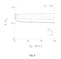
- FIG. 3 graphically illustrates how the energy of BS electrons emitted from a test sample depends on the elemental constitution of that sample.
- FIG. 1 is a highly schematic depiction of a charged-particle microscope 400 , which, in this case, is a SEM.
- the microscope 400 comprises a particle-optical column 402 , which produces a beam 404 of input charged particles (in this case, an electron beam).
- the particle-optical column 402 is mounted on a vacuum chamber 406 , which comprises a sample holder/stage 408 for holding a sample 410 .
- the vacuum chamber 406 is evacuated using vacuum pumps (not depicted).
- the particle-optical column 402 comprises an electron source 412 (such as a Schottky gun), lenses 414 , 416 to focus the electron beam 404 onto the sample 410 , and a deflection unit 418 (to perform beam steering/scanning of the beam 404 ).
- the apparatus 400 further comprises a controller/computer processing apparatus 424 for controlling inter alia the deflection unit 418 , lenses 414 , 416 and detectors 100 , 420 , and displaying information gathered from the detectors 100 , 420 on a display unit 426 .
- the detectors 420 , 100 are chosen from a variety of possible detector types that can be used to examine different types of output radiation emanating from the sample 410 in response to irradiation by the input beam 404 . In the apparatus depicted here, the following detector choices have been made:
- output radiation comprising, for example, X-rays, infrared/visible/ultraviolet light, secondary electrons and backscattered (BS) electrons—emanates from the sample 410 .
- output radiation is position-sensitive (due to said scanning motion)
- the information obtained from the detectors 100 , 420 will also be position-dependent.
- This fact allows the output of detector 420 to be used to produce a BS electron image of (part of) the sample 410 , which image is basically a map of an output of detector 420 as a function of scan-path position on the sample 410 .
- the signals from the detectors 100 , 420 are processed by the controller 424 , and displayed on display unit 426 .
- processing may include operations such as combining, integrating, subtracting, false colouring, edge enhancing, and other processing known to the skilled artisan.
- automated recognition processes e.g. as used for particle analysis
- the controller 424 and/or a dedicated separate processing unit (not shown)—can be used to perform the following actions:
- FIGS. 2A , 2 B and 2 C illustrate the effect of a particular embodiment of the current invention as enacted using a set-up as set forth in Embodiment 1 above.
- the figures all show part of the same sample 410 , which in this case comprises tin (Sn) droplets sputtered on carbon (C), imaged using BS electrons in a SEM on the basis of the following imaging parameters:
- FIG. 2A shows a conventional BS electron image of part of the employed sample 410 , being an averaged image derived from the set ⁇ I j ⁇ .
- this image is convoluted/unresolved as regards the energies (E) and numbers (N) of BS electrons triggering the detection events used to assemble the image.
- E energies
- N numbers
- the image in FIG. 2A can be deconvolved/resolved into a pair of separate maps.
- FIG. 2B shows the subject of FIG. 2A , but now rendered using the current invention as a first-type map (E-map) as alluded to above, and revealing compositional information of the employed sample 410 .
- the contrast-to-noise ratio (CNR) for the depicted map is ca. 3.56.
- FIG. 2C also shows the subject of FIG. 2A , but now rendered using the current invention as a second-type map (N-map) as alluded to above, and revealing inter alia (mostly) topographical information of the employed sample 410 .
- FIG. 3 graphically illustrates how the energy of BS electrons emitted from a test sample depends on the elemental constitution of that sample.
- the graph plots detected BS electron energy E (normalized to the landing energy E o of the input beam) as a function of said landing energy E o , for test samples comprising pure Au, Cu, Si and C.
- the fact that the plotted E-curves are clearly separated from one another over most of their extent (above about E o ⁇ 1 keV) illustrates the type of composition-dependent contrast that underlies the concept of an E-map as referred to above.
Landscapes
- Chemical & Material Sciences (AREA)
- Analytical Chemistry (AREA)
- Engineering & Computer Science (AREA)
- Computer Vision & Pattern Recognition (AREA)
- Physics & Mathematics (AREA)
- Health & Medical Sciences (AREA)
- Life Sciences & Earth Sciences (AREA)
- Biochemistry (AREA)
- General Health & Medical Sciences (AREA)
- General Physics & Mathematics (AREA)
- Immunology (AREA)
- Pathology (AREA)
- Analysing Materials By The Use Of Radiation (AREA)
- Image Processing (AREA)
Applications Claiming Priority (3)
| Application Number | Priority Date | Filing Date | Title |
|---|---|---|---|
| EP13195289 | 2013-12-02 | ||
| EP13195289.7 | 2013-12-02 | ||
| EP13195289.7A EP2879156A1 (en) | 2013-12-02 | 2013-12-02 | Charged-particle microscopy with enhanced electron detection |
Publications (2)
| Publication Number | Publication Date |
|---|---|
| US20150155131A1 US20150155131A1 (en) | 2015-06-04 |
| US9208993B2 true US9208993B2 (en) | 2015-12-08 |
Family
ID=49674236
Family Applications (1)
| Application Number | Title | Priority Date | Filing Date |
|---|---|---|---|
| US14/558,334 Active US9208993B2 (en) | 2013-12-02 | 2014-12-02 | Charged-particle microscopy with enhanced electron detection |
Country Status (4)
| Country | Link |
|---|---|
| US (1) | US9208993B2 (enExample) |
| EP (2) | EP2879156A1 (enExample) |
| JP (1) | JP6294216B2 (enExample) |
| CN (1) | CN104681382B (enExample) |
Families Citing this family (8)
| Publication number | Priority date | Publication date | Assignee | Title |
|---|---|---|---|---|
| EP3040714A1 (en) | 2014-12-30 | 2016-07-06 | Fei Company | Charged Particle Microscope with improved spectroscopic functionality |
| EP3106862B1 (en) | 2015-06-18 | 2019-01-16 | FEI Company | Method of ptychographic imaging |
| US10122946B2 (en) | 2015-11-11 | 2018-11-06 | Fei Company | Method for detecting particulate radiation |
| US10685759B2 (en) * | 2017-01-16 | 2020-06-16 | Fei Company | Statistical analysis in X-ray imaging |
| JP6796616B2 (ja) * | 2018-05-24 | 2020-12-09 | 日本電子株式会社 | 荷電粒子線装置および画像取得方法 |
| JP7072457B2 (ja) * | 2018-07-12 | 2022-05-20 | 株式会社堀場製作所 | 試料分析装置、電子顕微鏡、及び集光ミラーユニット |
| EP3726206B1 (en) * | 2019-03-26 | 2022-11-02 | FEI Company | Methods and systems for inclusion analysis |
| US10928336B1 (en) * | 2019-07-29 | 2021-02-23 | Applied Materials Israel Ltd. | X-ray based evaluation of a status of a structure of a substrate |
Citations (12)
| Publication number | Priority date | Publication date | Assignee | Title |
|---|---|---|---|---|
| WO2000070646A1 (en) | 1999-05-14 | 2000-11-23 | Applied Materials, Inc. | Secondary electron spectroscopy method and system |
| WO2003003402A1 (en) | 2001-06-29 | 2003-01-09 | Kla-Tencor Corporation | Energy filter multiplexing |
| US20040188611A1 (en) * | 2003-01-06 | 2004-09-30 | Shuichi Takeuchi | Scanning electron microscope and sample observing method using it |
| JP2005134181A (ja) | 2003-10-29 | 2005-05-26 | Jeol Ltd | データ処理方法及び分析装置 |
| US20050134181A1 (en) | 2003-12-19 | 2005-06-23 | Baocai Jang | Pulsed high-power flash lamps made of compound quartz glass tubes and process for manufacture thereof |
| WO2006019564A2 (en) | 2004-07-16 | 2006-02-23 | Tangle, Inc. | Therapeutic hand toys |
| WO2006109564A1 (ja) | 2005-04-11 | 2006-10-19 | Shimadzu Corporation | 走査ビーム装置のデータ処理方法 |
| US20080251718A1 (en) * | 2007-04-16 | 2008-10-16 | Ebara Corporation | Electron beam apparatus and sample observation method using the same |
| WO2009079195A1 (en) | 2007-12-17 | 2009-06-25 | Alis Corporation | Ion beam imaging |
| US20120032078A1 (en) * | 2010-08-04 | 2012-02-09 | Fei Company | Backscatter Reduction in Thin Electron Detectors |
| US20130054153A1 (en) | 2011-03-23 | 2013-02-28 | Tescan, A.S. | Method and apparatus for material analysis by a focused electron beam using characteristic x-rays and back-scattered electrons |
| EP2665083A2 (en) | 2012-05-17 | 2013-11-20 | Fei Company | Scanning microscope having an adaptive scan |
Family Cites Families (2)
| Publication number | Priority date | Publication date | Assignee | Title |
|---|---|---|---|---|
| JP2007220317A (ja) * | 2006-02-14 | 2007-08-30 | Jeol Ltd | 電子ビーム検査方法および装置 |
| EP2648208B1 (en) * | 2012-04-05 | 2017-08-09 | Fei Company | Charged-particle microscope providing depth-resolved imagery |
-
2013
- 2013-12-02 EP EP13195289.7A patent/EP2879156A1/en not_active Withdrawn
-
2014
- 2014-11-28 EP EP14195296.0A patent/EP2879157B1/en active Active
- 2014-12-01 JP JP2014243188A patent/JP6294216B2/ja active Active
- 2014-12-02 CN CN201410718566.8A patent/CN104681382B/zh active Active
- 2014-12-02 US US14/558,334 patent/US9208993B2/en active Active
Patent Citations (12)
| Publication number | Priority date | Publication date | Assignee | Title |
|---|---|---|---|---|
| WO2000070646A1 (en) | 1999-05-14 | 2000-11-23 | Applied Materials, Inc. | Secondary electron spectroscopy method and system |
| WO2003003402A1 (en) | 2001-06-29 | 2003-01-09 | Kla-Tencor Corporation | Energy filter multiplexing |
| US20040188611A1 (en) * | 2003-01-06 | 2004-09-30 | Shuichi Takeuchi | Scanning electron microscope and sample observing method using it |
| JP2005134181A (ja) | 2003-10-29 | 2005-05-26 | Jeol Ltd | データ処理方法及び分析装置 |
| US20050134181A1 (en) | 2003-12-19 | 2005-06-23 | Baocai Jang | Pulsed high-power flash lamps made of compound quartz glass tubes and process for manufacture thereof |
| WO2006019564A2 (en) | 2004-07-16 | 2006-02-23 | Tangle, Inc. | Therapeutic hand toys |
| WO2006109564A1 (ja) | 2005-04-11 | 2006-10-19 | Shimadzu Corporation | 走査ビーム装置のデータ処理方法 |
| US20080251718A1 (en) * | 2007-04-16 | 2008-10-16 | Ebara Corporation | Electron beam apparatus and sample observation method using the same |
| WO2009079195A1 (en) | 2007-12-17 | 2009-06-25 | Alis Corporation | Ion beam imaging |
| US20120032078A1 (en) * | 2010-08-04 | 2012-02-09 | Fei Company | Backscatter Reduction in Thin Electron Detectors |
| US20130054153A1 (en) | 2011-03-23 | 2013-02-28 | Tescan, A.S. | Method and apparatus for material analysis by a focused electron beam using characteristic x-rays and back-scattered electrons |
| EP2665083A2 (en) | 2012-05-17 | 2013-11-20 | Fei Company | Scanning microscope having an adaptive scan |
Non-Patent Citations (2)
| Title |
|---|
| Sznitman, Raphael, et al. "Efficient Scanning for EM Based Target Localization," Medical Image Computing and Computer-Assisted Intervention, 2012, pp. 337-344. |
| Sznitman, Raphael, et al., "Efficient Scanning for EM Based Target Localization", Medical Image Computing and Computer-Assisted Intervention Miccai, 2012, Berlin, Heidelberg, pp. 337-344. |
Also Published As
| Publication number | Publication date |
|---|---|
| CN104681382B (zh) | 2017-07-07 |
| US20150155131A1 (en) | 2015-06-04 |
| CN104681382A (zh) | 2015-06-03 |
| EP2879157A1 (en) | 2015-06-03 |
| JP2015106565A (ja) | 2015-06-08 |
| EP2879156A1 (en) | 2015-06-03 |
| JP6294216B2 (ja) | 2018-03-14 |
| EP2879157B1 (en) | 2016-01-13 |
Similar Documents
| Publication | Publication Date | Title |
|---|---|---|
| US9208993B2 (en) | Charged-particle microscopy with enhanced electron detection | |
| US10620142B2 (en) | X-ray spectroscopy in a charged-particle microscope | |
| EP2963673B1 (en) | Computational scanning microscopy with improved resolution | |
| US9618460B2 (en) | Method of performing tomographic imaging of a sample in a charged-particle microscope | |
| EP2525385A1 (en) | Charged-particle microscope | |
| US9812287B2 (en) | Charged particle microscope with improved spectroscopic functionality | |
| JP5050705B2 (ja) | 質量分析装置 | |
| CN103718268A (zh) | 带电粒子线装置 | |
| JP6155123B2 (ja) | 合成されたスペクトルデータを用いた分光法 | |
| CN109411320B (zh) | 透射带电粒子显微镜中的衍射图案检测 | |
| US9805910B1 (en) | Automated SEM nanoprobe tool | |
| EP3240013B1 (en) | Three-dimensional imaging in charged-particle microscopy | |
| US20180233322A1 (en) | Emission noise correction of a charged particle source | |
| KR20200138659A (ko) | 하전 입자 현미경을 사용한 샘플 검사 방법 | |
| JP7068811B2 (ja) | X線イメージングの統計的分析 | |
| EP2698805A1 (en) | Method of performing EDX in a charged-particle microscope | |
| CN120177530A (zh) | 使用带电粒子束和有源像素控制传感器来分析样品的系统和方法 | |
| KR101413287B1 (ko) | 입자빔의 방출 이미지 획득 장치 및 방법 | |
| JP2004354091A (ja) | 基板検査装置、基板検査方法および半導体装置の製造方法 |
Legal Events
| Date | Code | Title | Description |
|---|---|---|---|
| AS | Assignment |
Owner name: FEI COMPANY, OREGON Free format text: ASSIGNMENT OF ASSIGNORS INTEREST;ASSIGNORS:SLUIJTERMAN, ALBERTUS A. S.;BOSCH, ERIC G. T.;REEL/FRAME:034427/0127 Effective date: 20140908 |
|
| STCF | Information on status: patent grant |
Free format text: PATENTED CASE |
|
| MAFP | Maintenance fee payment |
Free format text: PAYMENT OF MAINTENANCE FEE, 4TH YEAR, LARGE ENTITY (ORIGINAL EVENT CODE: M1551); ENTITY STATUS OF PATENT OWNER: LARGE ENTITY Year of fee payment: 4 |
|
| MAFP | Maintenance fee payment |
Free format text: PAYMENT OF MAINTENANCE FEE, 8TH YEAR, LARGE ENTITY (ORIGINAL EVENT CODE: M1552); ENTITY STATUS OF PATENT OWNER: LARGE ENTITY Year of fee payment: 8 |