US9202707B2 - Semiconductor device manufacturing method - Google Patents
Semiconductor device manufacturing method Download PDFInfo
- Publication number
- US9202707B2 US9202707B2 US14/376,644 US201314376644A US9202707B2 US 9202707 B2 US9202707 B2 US 9202707B2 US 201314376644 A US201314376644 A US 201314376644A US 9202707 B2 US9202707 B2 US 9202707B2
- Authority
- US
- United States
- Prior art keywords
- film
- etching
- plasma
- torr
- photoresist layer
- Prior art date
- Legal status (The legal status is an assumption and is not a legal conclusion. Google has not performed a legal analysis and makes no representation as to the accuracy of the status listed.)
- Active
Links
Images


Classifications
-
- H01L21/3065—
-
- H—ELECTRICITY
- H10—SEMICONDUCTOR DEVICES; ELECTRIC SOLID-STATE DEVICES NOT OTHERWISE PROVIDED FOR
- H10P—GENERIC PROCESSES OR APPARATUS FOR THE MANUFACTURE OR TREATMENT OF DEVICES COVERED BY CLASS H10
- H10P50/00—Etching of wafers, substrates or parts of devices
- H10P50/20—Dry etching; Plasma etching; Reactive-ion etching
- H10P50/24—Dry etching; Plasma etching; Reactive-ion etching of semiconductor materials
- H10P50/242—Dry etching; Plasma etching; Reactive-ion etching of semiconductor materials of Group IV materials
-
- H—ELECTRICITY
- H01—ELECTRIC ELEMENTS
- H01J—ELECTRIC DISCHARGE TUBES OR DISCHARGE LAMPS
- H01J37/00—Discharge tubes with provision for introducing objects or material to be exposed to the discharge, e.g. for the purpose of examination or processing thereof
- H01J37/32—Gas-filled discharge tubes
- H01J37/32009—Arrangements for generation of plasma specially adapted for examination or treatment of objects, e.g. plasma sources
- H01J37/32082—Radio frequency generated discharge
- H01J37/32091—Radio frequency generated discharge the radio frequency energy being capacitively coupled to the plasma
-
- H—ELECTRICITY
- H01—ELECTRIC ELEMENTS
- H01J—ELECTRIC DISCHARGE TUBES OR DISCHARGE LAMPS
- H01J37/00—Discharge tubes with provision for introducing objects or material to be exposed to the discharge, e.g. for the purpose of examination or processing thereof
- H01J37/32—Gas-filled discharge tubes
- H01J37/32009—Arrangements for generation of plasma specially adapted for examination or treatment of objects, e.g. plasma sources
- H01J37/32082—Radio frequency generated discharge
- H01J37/32137—Radio frequency generated discharge controlling of the discharge by modulation of energy
- H01J37/32155—Frequency modulation
- H01J37/32165—Plural frequencies
-
- H01L21/0273—
-
- H01L21/308—
-
- H01L21/31116—
-
- H01L21/31138—
-
- H01L21/31144—
-
- H01L21/76838—
-
- H01L27/11556—
-
- H01L27/11582—
-
- H—ELECTRICITY
- H10—SEMICONDUCTOR DEVICES; ELECTRIC SOLID-STATE DEVICES NOT OTHERWISE PROVIDED FOR
- H10B—ELECTRONIC MEMORY DEVICES
- H10B41/00—Electrically erasable-and-programmable ROM [EEPROM] devices comprising floating gates
- H10B41/20—Electrically erasable-and-programmable ROM [EEPROM] devices comprising floating gates characterised by three-dimensional [3D] arrangements, e.g. with cells on different height levels
- H10B41/23—Electrically erasable-and-programmable ROM [EEPROM] devices comprising floating gates characterised by three-dimensional [3D] arrangements, e.g. with cells on different height levels with source and drain on different levels, e.g. with sloping channels
- H10B41/27—Electrically erasable-and-programmable ROM [EEPROM] devices comprising floating gates characterised by three-dimensional [3D] arrangements, e.g. with cells on different height levels with source and drain on different levels, e.g. with sloping channels the channels comprising vertical portions, e.g. U-shaped channels
-
- H—ELECTRICITY
- H10—SEMICONDUCTOR DEVICES; ELECTRIC SOLID-STATE DEVICES NOT OTHERWISE PROVIDED FOR
- H10B—ELECTRONIC MEMORY DEVICES
- H10B43/00—EEPROM devices comprising charge-trapping gate insulators
- H10B43/20—EEPROM devices comprising charge-trapping gate insulators characterised by three-dimensional [3D] arrangements, e.g. with cells on different height levels
- H10B43/23—EEPROM devices comprising charge-trapping gate insulators characterised by three-dimensional [3D] arrangements, e.g. with cells on different height levels with source and drain on different levels, e.g. with sloping channels
- H10B43/27—EEPROM devices comprising charge-trapping gate insulators characterised by three-dimensional [3D] arrangements, e.g. with cells on different height levels with source and drain on different levels, e.g. with sloping channels the channels comprising vertical portions, e.g. U-shaped channels
-
- H—ELECTRICITY
- H10—SEMICONDUCTOR DEVICES; ELECTRIC SOLID-STATE DEVICES NOT OTHERWISE PROVIDED FOR
- H10P—GENERIC PROCESSES OR APPARATUS FOR THE MANUFACTURE OR TREATMENT OF DEVICES COVERED BY CLASS H10
- H10P50/00—Etching of wafers, substrates or parts of devices
- H10P50/20—Dry etching; Plasma etching; Reactive-ion etching
- H10P50/28—Dry etching; Plasma etching; Reactive-ion etching of insulating materials
- H10P50/282—Dry etching; Plasma etching; Reactive-ion etching of insulating materials of inorganic materials
- H10P50/283—Dry etching; Plasma etching; Reactive-ion etching of insulating materials of inorganic materials by chemical means
-
- H—ELECTRICITY
- H10—SEMICONDUCTOR DEVICES; ELECTRIC SOLID-STATE DEVICES NOT OTHERWISE PROVIDED FOR
- H10P—GENERIC PROCESSES OR APPARATUS FOR THE MANUFACTURE OR TREATMENT OF DEVICES COVERED BY CLASS H10
- H10P50/00—Etching of wafers, substrates or parts of devices
- H10P50/20—Dry etching; Plasma etching; Reactive-ion etching
- H10P50/28—Dry etching; Plasma etching; Reactive-ion etching of insulating materials
- H10P50/286—Dry etching; Plasma etching; Reactive-ion etching of insulating materials of organic materials
- H10P50/287—Dry etching; Plasma etching; Reactive-ion etching of insulating materials of organic materials by chemical means
-
- H—ELECTRICITY
- H10—SEMICONDUCTOR DEVICES; ELECTRIC SOLID-STATE DEVICES NOT OTHERWISE PROVIDED FOR
- H10P—GENERIC PROCESSES OR APPARATUS FOR THE MANUFACTURE OR TREATMENT OF DEVICES COVERED BY CLASS H10
- H10P50/00—Etching of wafers, substrates or parts of devices
- H10P50/69—Etching of wafers, substrates or parts of devices using masks for semiconductor materials
- H10P50/691—Etching of wafers, substrates or parts of devices using masks for semiconductor materials for Group V materials or Group III-V materials
-
- H—ELECTRICITY
- H10—SEMICONDUCTOR DEVICES; ELECTRIC SOLID-STATE DEVICES NOT OTHERWISE PROVIDED FOR
- H10P—GENERIC PROCESSES OR APPARATUS FOR THE MANUFACTURE OR TREATMENT OF DEVICES COVERED BY CLASS H10
- H10P50/00—Etching of wafers, substrates or parts of devices
- H10P50/73—Etching of wafers, substrates or parts of devices using masks for insulating materials
-
- H—ELECTRICITY
- H10—SEMICONDUCTOR DEVICES; ELECTRIC SOLID-STATE DEVICES NOT OTHERWISE PROVIDED FOR
- H10P—GENERIC PROCESSES OR APPARATUS FOR THE MANUFACTURE OR TREATMENT OF DEVICES COVERED BY CLASS H10
- H10P76/00—Manufacture or treatment of masks on semiconductor bodies, e.g. by lithography or photolithography
- H10P76/20—Manufacture or treatment of masks on semiconductor bodies, e.g. by lithography or photolithography of masks comprising organic materials
- H10P76/204—Manufacture or treatment of masks on semiconductor bodies, e.g. by lithography or photolithography of masks comprising organic materials of organic photoresist masks
-
- H—ELECTRICITY
- H10—SEMICONDUCTOR DEVICES; ELECTRIC SOLID-STATE DEVICES NOT OTHERWISE PROVIDED FOR
- H10W—GENERIC PACKAGES, INTERCONNECTIONS, CONNECTORS OR OTHER CONSTRUCTIONAL DETAILS OF DEVICES COVERED BY CLASS H10
- H10W20/00—Interconnections in chips, wafers or substrates
- H10W20/01—Manufacture or treatment
- H10W20/031—Manufacture or treatment of conductive parts of the interconnections
-
- H—ELECTRICITY
- H01—ELECTRIC ELEMENTS
- H01J—ELECTRIC DISCHARGE TUBES OR DISCHARGE LAMPS
- H01J2237/00—Discharge tubes exposing object to beam, e.g. for analysis treatment, etching, imaging
- H01J2237/32—Processing objects by plasma generation
- H01J2237/33—Processing objects by plasma generation characterised by the type of processing
- H01J2237/334—Etching
Definitions
- the present invention relates to a semiconductor device manufacturing method.
- Manufacturing a three-dimensional (3D) stacked semiconductor memory such as the 3D NAND flash memory includes a process of etching a multilayer stacked film into a stepped configuration using a plasma (see e.g. Patent Document 1).
- a plasma see e.g. Patent Document 1
- the above effect is achieved by decreasing an ion energy of ions that contribute to etching the mask material in the vertical direction so that etching in the vertical direction may be suppressed and encouraging isotropic etching by radicals.
- Patent Document 1 Japanese Laid-Open Patent Publication No. 2009-266944
- the etch rate of the mask material may decrease owing to the decrease in the ion energy. Accordingly, there is a demand for a method of increasing the etch rate for etching the mask material in the lateral direction while increasing throughput.
- one aspect of the present invention relates to providing a semiconductor device manufacturing method that is capable of increasing the etch rate for etching the mask material in the lateral direction and increasing throughput.
- a semiconductor device manufacturing method includes introducing a processing gas into a parallel plate type plasma processing apparatus including an upper electrode and a lower electrode, applying a high frequency power to the lower electrode, generating a plasma within the plasma processing apparatus, etching with the plasma a multilayer film including a first film and a second film with differing dielectric constants alternately stacked on a substrate using a photoresist layer arranged on the multilayer film as a mask, and forming the multilayer film into a stepped configuration.
- the semiconductor device manufacturing method includes a first step of etching the first film using the photoresist layer as the mask; a second step of adjusting a pressure within a processing chamber of the plasma processing apparatus to be greater than or equal to 6 Torr and less than or equal to 30 Torr, generating the plasma by applying a first high frequency power for biasing and a second high frequency power for plasma generation to the lower electrode, and etching the photoresist layer using the generated plasma to reduce an area of the photoresist layer in a lateral direction; and a third step of etching the second film using the photoresist layer and the first film as the mask.
- the first step through the third step are repeated a predetermined number of times.
- a semiconductor device manufacturing method may be provided that is capable of increasing the etch rate for etching the mask material in the lateral direction and increasing throughput.
- FIG. 1 schematically illustrates a configuration of a 3D stacked semiconductor memory according to an embodiment of the present invention
- FIG. 2 is a cross-sectional view along line 1 - 1 of FIG. 1 ;
- FIG. 3 is a longitudinal cross-sectional view illustrating an overall configuration of a semiconductor device manufacturing apparatus according to an embodiment of the present invention
- FIG. 4 illustrates etching steps of a semiconductor device manufacturing method according to an embodiment of the present invention
- FIG. 5 illustrates principles of etching executed on a semiconductor device according to an embodiment of the present invention
- FIG. 6 illustrates principles of etching executed on a semiconductor device according to an embodiment of the present invention
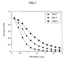
- FIG. 7 is a graph illustrating an ion incidence angle depending on the pressure
- FIG. 8 is a graph illustrating an ion incidence angle depending on the pressure
- FIG. 9 illustrates experimental results of lateral etching executed by a plasma processing apparatus A according to Embodiments 1, 2, and a Comparison Example
- FIG. 10 illustrates experimental results of lateral etching executed by a plasma processing apparatus B according to Embodiments 1, 2, and the Comparison Example.
- FIG. 11 illustrates graphs numerically representing the experimental results of FIGS. 9 and 10 .
- FIG. 1 is a perspective view schematically illustrating a configuration of 3D NAND flash memory.
- FIG. 2 is a cross-sectional view along line 1 - 1 of the 3D NAND flash memory illustrated in FIG. 1 .
- the 3D NAND flash memory is an example of a 3D stacked semiconductor memory.
- the 3D NAND flash memory 100 illustrated in FIG. 1 is made up of a plurality of blocks each constituting a unit for erasure, for example.
- two blocks BK 1 and BK 2 are illustrated.
- a source diffusion layer 102 formed within a semiconductor substrate may be provided as a common layer for all the blocks of the 3D NAND flash memory 100 , for example.
- the source diffusion layer 102 is connected to a source line SL via a contact plug PS.
- a first film and a second film having differing relative dielectric constants may be alternately stacked on the source diffusion layer 102 to form a stacked multilayer film, for example.
- the multilayer film is illustrated by a 6-layer structure in FIG. 1 for the sake of convenience, the multilayer film be made up of 16 layers, 32 layers, or even more layers.
- FIG. 1 five films corresponding to the five layers other than the uppermost layer of the multilayer structure are arranged into plates within each of the blocks BK 1 and BK 2 , and their X-direction end portions are arranged into a stepped configuration in order to establish contact with each of the films.
- the multilayer film is arranged into a pyramid shape.
- the lowermost layer of the multilayer film corresponds to a source line side select gate line SGS, and the four layers other than the lowermost layer and the uppermost layer correspond to word lines WL.
- the uppermost layer is made up of a plurality of conductive lines extending in the X direction.
- six conductive lines may be arranged within one block BK 1 .
- the six conductive lines of the uppermost layer may correspond to six bit line side select gate lines SGD.
- a plurality of active layers AC for configuring a NAND cell unit are arranged into columns extending in the Z direction (i.e. vertical direction with respect to semiconductor substrate surface) to penetrate through the plurality of layers and reach the source diffusion layer 102 .
- a plurality of bit lines BL extending in the Y direction are connected to the upper ends of the plurality of active layers AC.
- the source line side select gate line SGS is connected to a leader line SGS 1 extending in the X direction via a contact plug PSG.
- the word lines WL are connected to leader lines W 1 -W 4 extending in the X direction via contact plugs PW 1 -PW 4 .
- bit line side select gate lines SGD are connected to leader lines SGD 1 extending in the X direction via contact plugs PSD.
- the plurality of bit lines BL, the leader lines SGD 1 , and the leader lines WL 1 -WL 4 may be made of metal, for example.
- FIG. 2 is a cross-sectional view along line 1 - 1 of FIG. 1 .
- the source line side select gate line SGS and word lines WL 1 -WL 4 are connected to a transistor Tr included in a driver (not shown) via the contact plug PSG and the contact plugs PW 1 -PW 4 , which establish connection with the leader line SGS 1 and the leader lines W 1 -W 4 extending in the X direction.
- the plasma processing apparatus 10 illustrated in FIG. 3 is configured as a lower side dual frequency parallel plate type plasma etching apparatus (capacitively coupled plasma etching apparatus).
- the plasma processing apparatus 10 includes a cylindrical vacuum chamber (processing chamber) 11 (simply referred to as “chamber” hereinafter) made of aluminum having an alumite-treated (anodized) surface, for example.
- the chamber 11 may be grounded, for example.
- a mounting table 12 configured to hold a semiconductor wafer W (hereinafter, simply referred to as a “wafer W”) thereon as a workpiece is arranged within the chamber 11 .
- the mounting table 12 may be made of aluminum, for example, and is supported on a cylindrical support 16 via an insulating cylindrical holder 14 .
- the cylindrical support 16 extends vertically upward from a bottom of the chamber 11 .
- a focus ring 18 that may be made of silicon, for example, is arranged on a top surface of the mounting table to surround the outer edge of an electrostatic chuck 40 .
- An exhaust path 20 is formed between a sidewall of the chamber 11 and the cylindrical support 16 .
- a ring-shaped baffle plate 22 is arranged in the exhaust path 20 .
- An exhaust port 24 is formed at a bottom portion of the exhaust path 20 and is connected to an exhaust device 28 via an exhaust line 26 .
- the exhaust device 28 includes a vacuum pump (not shown) and is configured to depressurize a processing space within the chamber 11 to a predetermined vacuum level.
- a gate valve 30 configured to open/close an entry/exit port for the wafer W is provided at the sidewall of the chamber 11 .
- a first high frequency power supply 31 for drawing ions from within the plasma (for biasing) and a second high frequency power supply 32 for plasma generation are electrically connected to the mounting table 12 via a matching unit 33 and a matching unit 34 , respectively.
- the first high frequency power supply 31 is configured to apply to the mounting table 12 a first high frequency power having a suitable frequency such as 3.2 MHz for drawing ions from within a plasma.
- the second high frequency power supply 31 is configured to apply to the mounting table 12 a second high frequency power having a frequency such as 100 MHz for generating a plasma within the chamber 11 .
- the mounting table 12 also acts as a lower electrode.
- a shower head 38 which is described below, is provided at a ceiling portion of the chamber 11 .
- the shower head 38 acts as an upper electrode at a ground potential. In this way, the second high frequency power from the second high frequency power supply 32 is capacitively applied between the mounting table 12 and the shower head 38 .
- the electrostatic chuck 40 configured to hold the wafer W by an electrostatic attractive force is provided on the top surface of the mounting table 12 .
- the electrostatic chuck 40 includes an electrode 40 a that is made of a conductive film and is arranged between a pair of insulating films.
- a DC voltage supply 42 is electrically connected to the electrode 40 a via a switch 43 .
- the electrostatic chuck 40 electrostatically attracts and holds the wafer W by a Coulomb force that is generated when a voltage is applied thereto from the DC voltage supply 42 .
- a heat transfer gas supply source 52 is configured to supply a heat transfer gas such as He gas between the backside surface of the wafer W and the top surface of the electrostatic chuck 40 through a gas supply line 54 .
- the shower head 38 disposed at the ceiling portion of the chamber 11 includes an electrode plate 56 having multiple gas holes 56 a and an electrode supporting body 58 configured to detachably hold the electrode plate 56 .
- the gas supply source 62 supplies gas to the shower head 38 via a gas supply pipe 64 , which is connected to a gas inlet 60 a . In this way, the gas may be introduced into the chamber 11 from the multiple gas holes 56 a.
- a magnet 66 is arranged to extend annularly or concentrically around the chamber 11 such that the magnetic force of the magnet 66 may act to keep plasma confined within a plasma generation space of the chamber 11 .
- a coolant path 70 is formed within the mounting table 12 .
- a coolant cooled to a predetermined temperature is supplied to the coolant path 70 from a chiller unit 71 via pipes 72 and 73 .
- a heater 75 is arranged at the lower side of the electrostatic chuck 40 .
- a desired AC voltage is applied to the heater 75 from an AC power supply 44 .
- the temperature of the wafer W may be adjusted to a desired temperature through cooling by the chiller unit 71 and heating by the heater 75 . Note that such temperature control is performed based on a command from a control device 80 .
- the control device 80 is configured to control the individual components of the plasma processing apparatus 10 such as the exhaust device 28 , the AC power supply 44 , the DC voltage supply 42 , the switch 43 for the electrostatic chuck, the first high frequency power supply 31 , the second high frequency power supply 32 , the matching units 33 and 34 , the heat transfer gas supply source 52 , the gas supply source 62 , and the chiller unit 71 .
- the control device 80 is also connected to a host computer (not shown).
- the control device 80 includes a CPU (Central Processing Unit), a ROM (Read Only Memory), and a RAM (Random Access Memory), which are not shown.
- the CPU executes a plasma process according to various recipes stored in a storage unit (not shown).
- the storage unit storing the recipes may be configured by RAM or ROM using a semiconductor memory, a magnetic disk, or an optical disk, for example.
- the recipes may be stored in a storage medium and loaded in the storage unit via a driver (not shown), for example. Alternatively, the recipes may be downloaded to the storage unit via a network (not shown), for example.
- a DSP digital signal processor
- the functions of the control device 80 may be implemented by software, hardware, or a combination thereof.
- the gate valve 30 When performing an etching process using the plasma processing apparatus 10 having the above-described configuration, first, the gate valve 30 is opened, and the wafer W is loaded into the chamber 11 while being held by a transfer arm. Then, the wafer W is held by pusher pins (not shown), and the wafer W is placed on the electrostatic chuck 40 when the pusher pins are lowered. After the wafer W is loaded, the gate valve 30 is closed. Then, an etching gas is introduced into the chamber 11 from the gas supply source 62 at a predetermined flow rate and flow rate ratio, and the internal pressure of the chamber 11 is reduced to a predetermined pressure by the exhaust device 28 .
- high frequency powers at predetermined power levels are supplied to the mounting table 12 from the first high frequency power supply 31 and the second high frequency power supply 32 .
- a voltage from the DC voltage supply 42 is applied to the electrode 40 a of the electrostatic chuck 40 so that the wafer W may be fixed to the electrostatic chuck 40 .
- the heat transfer gas supply source 52 supplies a heat transfer gas such as He gas between the top surface of the electrostatic chuck 40 and the backside surface of the wafer W.
- Etching gas sprayed into the chamber 11 from the shower head 38 is excited into a plasma by the second high frequency power from the second high frequency power supply 32 .
- a plasma is generated within the plasma generation space between the upper electrode (shower head 38 ) and the lower electrode (mounting table 12 ), and a main surface of the wafer W is etched by the generated plasma. Also, ions within the plasma may be drawn toward the wafer W by the first high frequency power from the first high frequency power supply 31 .
- the wafer W is lifted and held by the pusher pins, the gate valve 30 is opened, and the transfer arm is introduced into the chamber 11 . Then, the pusher pins are lowered so that the wafer W may be held by the transfer arm. Then, the transfer arm exits the chamber 11 , and a next wafer W is loaded into the chamber 11 by the transfer arm.
- FIG. 4 illustrates an initial state (S 1 ) before etching steps of the present embodiment are started, a first step (S 2 ), a second step (S 3 ), a third step (S 4 ), and a final state (S 5 ) after the etching steps are completed.
- a stepped configuration is formed on a multilayer film.
- a 36-layer multilayer film ml having a first film 110 and a second film 120 alternately stacked on a substrate S is formed.
- the multilayer film ml may be a stacked film having at least 16 layers of the first film 110 and the second film 120 alternately arranged on each other, for example.
- the first film 110 and the second film 120 are insulating films having differing relative dielectric constants.
- a silicon oxide (SiO 2 ) film is used as the first film 110 and a silicon nitride (SiN) film is used as the second film 120 to form the multilayer film ml made up of films having differing relative dielectric constants.
- the combination of the first film 110 and the second film 120 is not limited to the above silicon oxide film/silicon nitride film combination.
- a polysilicon (impurity-doped) film may be used as the first film 110 and a polysilicon (non-doped) film may be used as the second film 120 .
- the first film 110 and the second film 120 have differing relative dielectric constants based on whether impurities are doped.
- a material such as boron may be doped as an impurity, for example.
- a silicon oxide (SiO 2 ) film may be used as the first film 110 and a polysilicon (impurity-doped) film may be used as the second film 120
- a silicon oxide (SiO 2 ) film may be used as the first film 110 and a polysilicon (non-doped) film may be used as the second film 120 .
- a photoresist layer PR that acts as a mask is arranged directly above the multilayer film ml. By etching the photoresist layer PR primarily in the lateral direction, a stepped configuration may be formed at the multilayer film ml.
- the photoresist layer PR may be made of an organic film or an amorphous carbon ( ⁇ -C) film, for example.
- the photoresist layer PR may be an i-line (365 nm wavelength) photoresist layer, for example.
- the photoresist layer PR is used as a mask to etch the silicon oxide (SiO 2 ) film corresponding to the first film 110 .
- a so-called normal etching process is performed where etching in the vertical direction is encouraged by the ion energy.
- the process conditions for this step are as follows:
- the photoresist layer PR is etched.
- the etch rate for etching in the lateral direction is increased with respect to the etch rate for etching in the vertical direction, and process conditions are optimized such that the photoresist layer PR may be etched in the lateral direction as much as possible.
- the process conditions for etching the photoresist layer PR in the lateral direction are described in detail below.
- the photoresist layer PR and the first film 110 are used as the mask to etch the second film 120 .
- etching in the vertical direction is encouraged by the ion energy, and the following process conditions are used:
- the first step through the third step are repeatedly executed.
- the multilayer ml may be formed into a stepped configuration.
- the so-called normal etching process is performed in which etching in the vertical direction is primarily encouraged.
- the second step calls for a technique for selectively etching the photoresist layer PR in the lateral direction rather than the vertical direction.
- a technique for actively etching the photoresist layer PR in the lateral direction has not been readily available.
- a technique has been used that involves suppressing etching in the vertical direction by decreasing the ion energy contributing to vertical etching of the photoresist layer PR and encouraging isotropic etching by radicals.
- this technique because the ion energy is decreased, the etch rate is decreased and a longer processing time is required, thereby leading to a decrease in throughput.
- the ion energy is increased by applying biasing power to the substrate S without implementing any countermeasures, although the lateral etch rate may be accelerated, the vertical etch rate is accelerated even further such that selective etching in the lateral direction becomes difficult.
- a technique is in demand for increasing a ratio of the lateral etch rate with respect to the vertical etch rate; namely, a photoresist layer trim ratio (lateral etch rate/vertical etch rate) corresponding to an index of etching in the lateral direction.
- a semiconductor device manufacturing method involves not only encouraging isotropic etching by radicals but also increasing a contribution ratio of ions to lateral etching over vertical etching and increasing the photoresist layer trim ratio. Accordingly, process conditions are adjusted so that incidence of ions in the lateral direction may be increased. In the following, measures for optimizing process conditions for increasing the etch rate in the lateral direction is described.
- a high frequency power for biasing is not applied to the lower electrode to draw ions from within a plasma in a vertical direction toward the substrate.
- the pressure is set to approximately several hundred mTorr upon performing the etching process.
- the relationship between the angle of ions incident on the substrate (ion angle) and the pressure is placed under scrutiny.
- ions having positive charges, electrons having negative charges, and radicals having neutral charges of a plasma exist within a plasma space.
- the radicals primarily contribute to chemical etching through a chemical reaction between the radicals and the stacked layer film, and the ions primarily contribute to physical etching through bombardment of the ions against the substrate.
- the radicals (O*) primarily contribute to isotropic etching of the photoresist layer PR.
- the direction of etching by the ions (O 2 +) depends on the ion angle.
- the incidence angle ⁇ of the ions is ideally 45 degrees.
- the incidence angle ⁇ of the ions is less than 45 degrees, etching in the vertical direction tends to be encouraged by the ions as the incidence angle ⁇ of the ions becomes smaller (i.e., as the incidence angle ⁇ of the ions comes closer to 0 degrees).
- the ratio of lateral etching by the ion energy is decreased.
- the incidence angle ⁇ of the ions when the incidence angle ⁇ of the ions is greater than 45 degrees, it becomes increasingly difficult for the ions to reach a bottom portion of a surface to be etched (side faces SW in FIG. 5 ) as the incidence angle ⁇ of the ions becomes greater (i.e., as the incidence angle ⁇ of the ions comes closer to 90 degrees). As a result, the contribution ratio of the ion energy to etching in the lateral direction is decreased.
- FIGS. 7 and 8 are graphs illustrating the relationship between the incidence angle of the ions and the pressure.
- the horizontal axis represents the incidence angle of the ions (ion angle) and the vertical axis represents the IADF (ion angle distribution function).
- the ions within a plasma may be oriented in various angles.
- the ion angle depends upon the pressure. Specifically, within a pressure region on the order of 100 mTorr, approximately 20% of the ions within the plasma are oriented at an ion diffusion angle (corresponding to the ion incidence angle) of one degree. At this angle, the ions hardly contribute to etching in the lateral direction. That is, as can be appreciated from the graphs of FIG.
- etching is performed under a high pressure range on the order of several Torr to increase the contribution ratio of the ions to etching in the lateral direction.
- the horizontal axis represents the pressure (Torr) and the vertical axis represents the FWHM (Full-Width Half-Maximum) of the ion angle.
- the FWHM of the ion angle corresponds to one half (1 ⁇ 2) of a value obtained by subtracting a minimum value of the angle distribution from a maximum value of the angle distribution.
- the FWHM is an index of the ion having the most representative energy among the ions within the plasma.
- the pressure is preferably adjusted such that the representative ion has an incidence angle of 45 degrees. In this way, the contribution of ions to etching in the lateral direction may be maximized.
- the pressure may be within a range of 6-30 Torr such that the FWHM of the ion angle may be within a range of 15-75 degrees.
- the etch rate for etching the photoresist layer PR may be increased and trimming at a high throughput may be enabled.
- the ions when the pressure is adjusted to a high pressure range of 6-30 Torr, the ions are accelerated and the ions may collide at a higher frequency when the ions enter the sheath region as illustrated in FIG. 5 .
- the ions when the ions enter the sheath region, the ions may form an angle more easily owing to the collision, and as a result, the ion angles of the ions within the sheath region may be increased.
- the pressure is below 6 Torr, the frequency of collision of the ions within the plasma before they reach the substrate may be reduced, and the ions within the sheath region are less likely to four angles.
- the ions are more likely to be incident in a vertical direction with respect to the substrate, and the contribution of the ions to etching in the lateral direction may be reduced relative to their contribution to etching in the vertical direction.
- the pressure is above 30 Torr, the frequency of collision of the ions within the plasma before they reach the substrate is increased such that the ion energy is reduced.
- the contribution of the ions to etching in the lateral direction may be reduced.
- the pressure within a processing chamber is adjusted to 6-30 Torr so that the ion diffusion angle of the ions within the plasma may be 15-75 degrees, and a high frequency power for plasma generation and a high frequency power for biasing are applied to the lower electrode.
- a plasma generated in this way is used to etch the photoresist layer PR to reduce the area of the photoresist layer PR in the lateral direction.
- the pressure within the processing chamber may be adjusted to be within a range of 10-26 Torr so that the ion diffusion angle may be within a range of 25-65 degrees.
- the pressure within the processing chamber may be adjusted to be within a range of 14-22 Torr so that the ion diffusion angle may be within a range of 35-55 degrees.
- FIG. 9 illustrates experimental results of using the lower side dual frequency power application type semiconductor device manufacturing apparatus (referred to as “plasma processing apparatus A” hereinafter) in which an electrode gap between the upper electrode and the lower electrode (referred to as “gap” hereinafter) is comparatively smaller.
- FIG. 10 illustrates experimental results of using the upper/lower side power application type semiconductor manufacturing apparatus (referred to as “plasma processing apparatus B” hereinafter) in which the gap between the upper electrode and the lower electrode is comparatively larger. Note that the plasma processing apparatus A and the plasma processing apparatus B are capacitively coupled plasma processing apparatuses.
- processing chamber seal refers to filling the processing chamber with oxygen (O 2 ) gas and closing an APC (automatic pressure controller) after the pressure within the processing chamber reaches a predetermined pressure to thereby seal the gas within the processing chamber.
- APC automatic pressure controller
- etching is performed under the above process conditions. Note that in the Comparative Example, the first high frequency power LF for drawing in ions from within the plasma is not applied. That is, in the Comparative Example, ions do not actively contribute to etching the photoresist layer PR, and etching is encouraged mainly by radicals as in the conventional method.
- Embodiment 1 a first high frequency power LF of 0.28 (W/cm 2 ) is applied to the lower electrode.
- a first high frequency power LF of 0.71 (W/cm 2 ) is applied to the lower electrode. Accordingly, in Embodiment 1 and Embodiment 2, etching is encouraged by ions and radicals. Thus, under a high pressure atmosphere, ions may actively contribute to etching in Embodiment 1 and Embodiment 2.
- the photoresist layer trim ratios in Embodiment 1 and Embodiment 2 are the same or higher than the photoresist layer trim ratio in the Comparative Example.
- the photoresist layer trim ratio in Embodiment 2 is the same as the photoresist layer trim ratio in the Comparative Example.
- the photoresist layer trim ratio in Embodiment 1 when the pressure is 5 Torr, and the photoresist layer trim ratios in Embodiment 1 and Embodiment 2 when the pressure is 9 Torr are higher than the photoresist layer trim ratio in the Comparative Example.
- the photoresist layer trim ratio in Embodiment 1 is approximately two times the photoresist layer trim ratio in the Comparative Example.
- the photoresist layer trim ratio may be increased as the pressure is increased and the first high frequency power LF is applied. That is, the above experimental results indicate that in the case where the plasma processing apparatus A is used, ions within the plasma may effectively contribute to etching in the lateral direction when the pressure within the processing chamber is higher than 5 Torr and the first high frequency power LF for biasing is within a range of 0.28-0.71 (W/cm 2 ).
- etching is performed under the above process conditions. Note that in the Comparative Example, the first high frequency power LF for drawing ions from within the plasma is not applied. That is, in the Comparative Example, ions do not actively contribute to etching the photoresist layer PR, and etching is encouraged mainly by radicals as in the conventional method.
- Embodiment 1 a first high frequency power LF of 0.28 (W/cm 2 ) is applied to the lower electrode.
- a first high frequency power LF of 0.71 (W/cm 2 ) is applied to the lower electrode. Accordingly, in Embodiment 1 and Embodiment 2, etching is encouraged by ions and radicals. Thus, under a high pressure atmosphere, ions are expected to actively contribute to etching in Embodiment 1 and Embodiment 2.
- FIG. 11 illustrates graphic comparisons of the experimental results of FIGS. 9 and 10 .
- the plasma processing apparatus A of FIG. 11 corresponds to the semiconductor device manufacturing apparatus that was used to execute the etching process under the process conditions indicated in FIG. 9 .
- the plasma processing apparatus B of FIG. 11 corresponds to the semiconductor device manufacturing apparatus that was used to execute the etching process under the process conditions indicated in FIG. 10 .
- the photoresist layer trim ratio is substantially increased compared to the photoresist layer trim ratio of the Comparative Example. That is, when a high frequency power LF for biasing is applied as in Embodiment 1 and Embodiment 2 and when the pressure is adjusted to a high pressure in the plasma processing apparatus A, a substantial increase in the photoresist trim ratio may be observed.
- the plasma processing apparatus B when a high frequency power LF for biasing is applied according to Embodiment 1 and Embodiment 2 and when the pressure is adjusted to 5 Torr, the photoresist layer trim ratio does not rise to a level as high as the photoresist layer trim ratio achieved by the plasma processing apparatus A. That is, when a high frequency power LF for biasing is applied as in Embodiment 1 and Embodiment 2 and the pressure is adjusted to a high pressure in the plasma processing apparatus B, the lateral etch rate tends to be lower compared to cases where a lower pressure is used and an increase in the lateral etch rate relative to an increase in the high frequency power LF is rather small.
- the photoresist layer trim ratio when the pressure is 5 Torr and a high frequency power LF of 500 W for biasing is applied in the plasma processing apparatus A, the photoresist layer trim ratio is greater than 0.6.
- the photoresist layer trim ratio when the pressure is 5 Torr and a high frequency power LF of 500 W for biasing is applied in the plasma processing apparatus B, the photoresist layer trim ratio is less than 0.4. That is, in this case, the photoresist layer trim ratio in the plasma processing apparatus A is approximately 1.5 times the photoresist layer trim ratio in the plasma processing apparatus B. Further, the photoresist layer trim ratio in the plasma processing apparatus A when the pressure is 9 Torr and a high frequency power LF of 500 W is applied is approximately 2 times the photoresist layer trim ratio in the plasma processing apparatus B when the pressure is 5 Torr.
- the gap between the upper electrode and the lower electrode in the plasma processing apparatus B is greater than the gap in the plasma processing apparatus A.
- the high frequency power for plasma generation is applied to the upper electrode, and as a result, a plasma is generated near the upper electrode.
- the high frequency power for plasma generation is applied to the lower electrode, and as a result, a plasma is generated near the lower electrode. Accordingly, in the plasma processing apparatus B, the travel distance of ions within the plasma before they reach the substrate is relatively long. Thus, in the plasma processing apparatus B, the ions within the plasma collide with numerous gases before they reach the substrate, and as a result, most of the ion energy may be depleted.
- the travel distance of ions within the plasma before they reach the substrate is relatively short. Accordingly, in the plasma processing apparatus A, the ions within the plasma are less likely to collide with gases before reaching the substrate in comparison to the plasma processing apparatus B. As a result, the loss of ion energy before the ions reach the substrate may not be so large in the plasma processing apparatus A.
- the gap between the upper electrode and the lower electrode is preferably arranged to be within a range of 20-40 mm and the high frequency power for biasing is preferably applied to the lower electrode.
- an inductively coupled plasma processing apparatus (not shown)
- a coil is arranged outside the chamber and a dielectric window is formed at a ceiling portion of the chamber positioned below the coil. Electromagnetic waves emitted from the coil pass through the dielectric window to be introduced into the chamber.
- the intensity distribution of the electromagnetic waves introduced into the chamber has a pattern substantially corresponding to the shape of the coil.
- the gap In order to prevent such unevenness in the plasma density, the gap needs to be widened to enable diffusion of the plasma. Thus, in view of such structural constraints of the inductively coupled plasma processing apparatus, a relatively wide gap needs to be secured in order to achieve in-plane uniformity for microfabrication.
- the travel distance of ions travelling from within the plasma to the substrate may be relatively long. Accordingly, even when the pressure is adjusted to a high pressure of several Torr, the ions within the plasma are likely to collide with numerous gases before reaching the substrate such that most of the ion energy may be depleted. As a result, etching in the lateral direction may not be adequately encouraged, and the lateral etch rate may not be adequately increased.
- the photoresist layer PR which is formed on the multilayer film ml, is etched by an etching process that satisfies all of the following process conditions (1)-(4).
- Etching is performed using a parallel plate type plasma processing apparatus (capacitively coupled plasma processing apparatus) in which the gap between the upper electrode and the lower electrode is 20-40 mm.
- the pressure within the processing chamber is adjusted to be greater than or equal to 6 Torr and less than or equal to 30 Torr such that the diffusion angle of the ions within the plasma may be greater than or equal to 15 degrees and less than or equal to 75 degrees.
- the high frequency power for biasing (LF) is applied to the lower electrode.
- a high frequency power of 0.28-0.71 (W/cm 2 ) is preferably applied as the high frequency power for biasing.
- the photoresist layer trim ratio may be increased and the lateral etch rate may be increased. Accordingly, in the second step of the present embodiment, the photoresist layer PR may be etched in the lateral direction at a desirable etch rate to reduce the area of the photoresist layer PR in the lateral direction. In this way, the throughput may be increased. Also, the photoresist layer PR may be prevented from being removed while the multilayer film ml is still being etched into a stepped configuration.
- O 2 gas process chamber seal
- a semiconductor device manufacturing method is not limited to the above embodiment, and for example, the processing gas used in the second step may include at least one gas selected from a group consisting of O 2 , H 2 , N 2 , CO, and CO 2 .
- the gas is supplied in a sealed state in the second step of the above embodiment, in other embodiments, a desired gas may be continually supplied in an ordinary manner at a predetermined gas flow rate.
- the workpiece subject to a plasma process in the present invention is not limited to a semiconductor wafer but may be a large substrate for a flat panel display (FPD), an electroluminescence (EL) element, or a substrate for a solar battery, for example.
- FPD flat panel display
- EL electroluminescence
- the pressure within the processing chamber may be adjusted to be greater than or equal to 10 Torr and less than or equal to 26 Torr in the second step.
- the pressure within the processing chamber may be adjusted to be greater than or equal to 14 Torr and less than or equal to 22 Torr in the second step.
- a high frequency power for biasing that is greater than or equal to 0.28 W/cm 2 and less than or equal to 0.71 W/cm 2 may be applied to the lower electrode in the second step.
- At least one gas selected from a group consisting of O 2 , H 2 , N 2 , CO, and CO 2 may be used as a processing gas in the second step.
- the first film may be made of a silicon oxide film and the second film may be made of a silicon nitride film.
- the multilayer film may have at least sixteen layers of the first film and the second film alternately stacked on each other.
Landscapes
- Physics & Mathematics (AREA)
- Engineering & Computer Science (AREA)
- Plasma & Fusion (AREA)
- Chemical & Material Sciences (AREA)
- Analytical Chemistry (AREA)
- Drying Of Semiconductors (AREA)
- Semiconductor Memories (AREA)
- Plasma Technology (AREA)
- Internal Circuitry In Semiconductor Integrated Circuit Devices (AREA)
- Non-Volatile Memory (AREA)
Abstract
Description
| |
30 mT (=3.99966 Pa) |
| First High Frequency Power/ |
1000/400 W (141.5 W/cm2, |
| High Frequency Power | 56.6 W/cm2) |
| Gas Type & Gas Flow Rate | O2/Ar/C4F6 = 30/1000/16 sccm |
| Pressure | 150 mT (=19.9983 Pa) |
| First High Frequency Power/ |
300/800 W (42.5 W/cm2, |
| High Frequency Power | 113.2 W/cm2) |
| Gas Type & Gas Flow Rate | CH2F2/Ar/C2 = 140/400/70 sccm |
| |
35 mm | ||
| High Frequency Power Application | Lower side dual | ||
| Method | frequency | ||
| Frequency of |
100 MHz | ||
| Power Supply (HF) | |||
| High Frequency Power of Second High | 1000 W (1.415 W/cm2) | ||
| Frequency Power Supply | |||
| Frequency of First High Frequency | 3.2 MHz | ||
| Power Supply (LF) | |||
| High Frequency Power of First High | Comparative Example: | ||
| Frequency Power Supply | 0 W/cm2 | ||
| Embodiment 1: | |||
| 200 W (0.28 W/cm2) | |||
| Embodiment 2: | |||
| 500 W (0.71 W/cm2) | |||
| Gas Type | O2 (Processing | ||
| chamber seal) | |||
| Heat | He | 20 | |
| Pressure | |||
| 3 Conditions: | |||
| 1, 5, 9 Torr | |||
| Gap | 87 mm | ||
| High Frequency Power Application | Upper/lower side dual | ||
| Method | frequency | ||
| Frequency of Second High Frequency | 60 MHz | ||
| Power Supply (HF) | |||
| High Frequency Power of Second High | 1000 W (1.415 W/cm2) | ||
| Frequency Power Supply | |||
| Frequency of First High Frequency | 13.56 MHz | ||
| Power Supply (LF) | |||
| High Frequency Power of First High | Comparative Example: | ||
| Frequency Power Supply | 0 W/cm2 | ||
| Embodiment 1: | |||
| 200 W (0.28 W/cm2) | |||
| Embodiment 2: | |||
| 500 W (0.71 W/cm2) | |||
| Gas Type | O2 (Processing chamber | ||
| seal) | |||
| Heat | He | 20 | |
| Pressure | |||
| 4 Conditions: | |||
| 0.1, 0.5, 1, 5 Torr | |||
- 10 plasma processing apparatus
- 11 chamber
- 12 mounting table (lower electrode)
- 31 first high frequency power supply (for biasing)
- 32 second high frequency power supply (for plasma generation)
- 38 shower head (upper electrode)
- 62 gas supply source
- 80 control device
- 110 first film
- 120 second film
- PR photoresist film
Claims (8)
Priority Applications (1)
| Application Number | Priority Date | Filing Date | Title |
|---|---|---|---|
| US14/376,644 US9202707B2 (en) | 2012-02-17 | 2013-02-05 | Semiconductor device manufacturing method |
Applications Claiming Priority (5)
| Application Number | Priority Date | Filing Date | Title |
|---|---|---|---|
| JP2012-033372 | 2012-02-17 | ||
| JP2012033372A JP5912637B2 (en) | 2012-02-17 | 2012-02-17 | Manufacturing method of semiconductor device |
| US201261603405P | 2012-02-27 | 2012-02-27 | |
| PCT/JP2013/052633 WO2013121936A1 (en) | 2012-02-17 | 2013-02-05 | Semiconductor device manufacturing method |
| US14/376,644 US9202707B2 (en) | 2012-02-17 | 2013-02-05 | Semiconductor device manufacturing method |
Publications (2)
| Publication Number | Publication Date |
|---|---|
| US20140363980A1 US20140363980A1 (en) | 2014-12-11 |
| US9202707B2 true US9202707B2 (en) | 2015-12-01 |
Family
ID=48984049
Family Applications (1)
| Application Number | Title | Priority Date | Filing Date |
|---|---|---|---|
| US14/376,644 Active US9202707B2 (en) | 2012-02-17 | 2013-02-05 | Semiconductor device manufacturing method |
Country Status (6)
| Country | Link |
|---|---|
| US (1) | US9202707B2 (en) |
| JP (1) | JP5912637B2 (en) |
| KR (1) | KR102038608B1 (en) |
| CN (1) | CN104081502B (en) |
| TW (1) | TW201351499A (en) |
| WO (1) | WO2013121936A1 (en) |
Cited By (4)
| Publication number | Priority date | Publication date | Assignee | Title |
|---|---|---|---|---|
| US10347502B2 (en) | 2017-09-07 | 2019-07-09 | Samsung Electronics Co., Ltd. | Methods for manufacturing semiconductor devices having three-dimensionally arranged memory cells |
| US10529732B2 (en) | 2018-04-18 | 2020-01-07 | Yangtze Memory Technologies Co., Ltd. | Method for forming staircase structure of three-dimensional memory device |
| US12283547B2 (en) | 2021-02-22 | 2025-04-22 | Yangtze Memory Technologies Co., Ltd. | Contact structures for three-dimensional memory devices and methods for forming the same |
| US12512329B2 (en) | 2023-04-06 | 2025-12-30 | Tokyo Electron Limited | Multi level contact etch |
Families Citing this family (425)
| Publication number | Priority date | Publication date | Assignee | Title |
|---|---|---|---|---|
| US10378106B2 (en) | 2008-11-14 | 2019-08-13 | Asm Ip Holding B.V. | Method of forming insulation film by modified PEALD |
| US9394608B2 (en) | 2009-04-06 | 2016-07-19 | Asm America, Inc. | Semiconductor processing reactor and components thereof |
| US12444651B2 (en) | 2009-08-04 | 2025-10-14 | Novellus Systems, Inc. | Tungsten feature fill with nucleation inhibition |
| US8802201B2 (en) | 2009-08-14 | 2014-08-12 | Asm America, Inc. | Systems and methods for thin-film deposition of metal oxides using excited nitrogen-oxygen species |
| US9312155B2 (en) | 2011-06-06 | 2016-04-12 | Asm Japan K.K. | High-throughput semiconductor-processing apparatus equipped with multiple dual-chamber modules |
| US9793148B2 (en) | 2011-06-22 | 2017-10-17 | Asm Japan K.K. | Method for positioning wafers in multiple wafer transport |
| US10364496B2 (en) | 2011-06-27 | 2019-07-30 | Asm Ip Holding B.V. | Dual section module having shared and unshared mass flow controllers |
| US10854498B2 (en) | 2011-07-15 | 2020-12-01 | Asm Ip Holding B.V. | Wafer-supporting device and method for producing same |
| US20130023129A1 (en) | 2011-07-20 | 2013-01-24 | Asm America, Inc. | Pressure transmitter for a semiconductor processing environment |
| US9017481B1 (en) | 2011-10-28 | 2015-04-28 | Asm America, Inc. | Process feed management for semiconductor substrate processing |
| US11437269B2 (en) | 2012-03-27 | 2022-09-06 | Novellus Systems, Inc. | Tungsten feature fill with nucleation inhibition |
| US8946830B2 (en) | 2012-04-04 | 2015-02-03 | Asm Ip Holdings B.V. | Metal oxide protective layer for a semiconductor device |
| US9558931B2 (en) | 2012-07-27 | 2017-01-31 | Asm Ip Holding B.V. | System and method for gas-phase sulfur passivation of a semiconductor surface |
| US9659799B2 (en) | 2012-08-28 | 2017-05-23 | Asm Ip Holding B.V. | Systems and methods for dynamic semiconductor process scheduling |
| US9021985B2 (en) | 2012-09-12 | 2015-05-05 | Asm Ip Holdings B.V. | Process gas management for an inductively-coupled plasma deposition reactor |
| US9324811B2 (en) | 2012-09-26 | 2016-04-26 | Asm Ip Holding B.V. | Structures and devices including a tensile-stressed silicon arsenic layer and methods of forming same |
| US10714315B2 (en) | 2012-10-12 | 2020-07-14 | Asm Ip Holdings B.V. | Semiconductor reaction chamber showerhead |
| US9640416B2 (en) | 2012-12-26 | 2017-05-02 | Asm Ip Holding B.V. | Single-and dual-chamber module-attachable wafer-handling chamber |
| US20160376700A1 (en) | 2013-02-01 | 2016-12-29 | Asm Ip Holding B.V. | System for treatment of deposition reactor |
| US9589770B2 (en) | 2013-03-08 | 2017-03-07 | Asm Ip Holding B.V. | Method and systems for in-situ formation of intermediate reactive species |
| US9484191B2 (en) | 2013-03-08 | 2016-11-01 | Asm Ip Holding B.V. | Pulsed remote plasma method and system |
| US9564309B2 (en) | 2013-03-14 | 2017-02-07 | Asm Ip Holding B.V. | Si precursors for deposition of SiN at low temperatures |
| US9824881B2 (en) | 2013-03-14 | 2017-11-21 | Asm Ip Holding B.V. | Si precursors for deposition of SiN at low temperatures |
| US8993054B2 (en) | 2013-07-12 | 2015-03-31 | Asm Ip Holding B.V. | Method and system to reduce outgassing in a reaction chamber |
| US9018111B2 (en) | 2013-07-22 | 2015-04-28 | Asm Ip Holding B.V. | Semiconductor reaction chamber with plasma capabilities |
| US9793115B2 (en) | 2013-08-14 | 2017-10-17 | Asm Ip Holding B.V. | Structures and devices including germanium-tin films and methods of forming same |
| US9240412B2 (en) | 2013-09-27 | 2016-01-19 | Asm Ip Holding B.V. | Semiconductor structure and device and methods of forming same using selective epitaxial process |
| US9556516B2 (en) | 2013-10-09 | 2017-01-31 | ASM IP Holding B.V | Method for forming Ti-containing film by PEALD using TDMAT or TDEAT |
| US9543140B2 (en) | 2013-10-16 | 2017-01-10 | Asm Ip Holding B.V. | Deposition of boron and carbon containing materials |
| US9576790B2 (en) | 2013-10-16 | 2017-02-21 | Asm Ip Holding B.V. | Deposition of boron and carbon containing materials |
| US9343308B2 (en) * | 2013-10-28 | 2016-05-17 | Asm Ip Holding B.V. | Method for trimming carbon-containing film at reduced trimming rate |
| US10179947B2 (en) | 2013-11-26 | 2019-01-15 | Asm Ip Holding B.V. | Method for forming conformal nitrided, oxidized, or carbonized dielectric film by atomic layer deposition |
| US9401273B2 (en) | 2013-12-11 | 2016-07-26 | Asm Ip Holding B.V. | Atomic layer deposition of silicon carbon nitride based materials |
| US10683571B2 (en) | 2014-02-25 | 2020-06-16 | Asm Ip Holding B.V. | Gas supply manifold and method of supplying gases to chamber using same |
| US9447498B2 (en) | 2014-03-18 | 2016-09-20 | Asm Ip Holding B.V. | Method for performing uniform processing in gas system-sharing multiple reaction chambers |
| US10167557B2 (en) | 2014-03-18 | 2019-01-01 | Asm Ip Holding B.V. | Gas distribution system, reactor including the system, and methods of using the same |
| US11015245B2 (en) | 2014-03-19 | 2021-05-25 | Asm Ip Holding B.V. | Gas-phase reactor and system having exhaust plenum and components thereof |
| US9404587B2 (en) | 2014-04-24 | 2016-08-02 | ASM IP Holding B.V | Lockout tagout for semiconductor vacuum valve |
| US10858737B2 (en) | 2014-07-28 | 2020-12-08 | Asm Ip Holding B.V. | Showerhead assembly and components thereof |
| US9543180B2 (en) | 2014-08-01 | 2017-01-10 | Asm Ip Holding B.V. | Apparatus and method for transporting wafers between wafer carrier and process tool under vacuum |
| US9890456B2 (en) | 2014-08-21 | 2018-02-13 | Asm Ip Holding B.V. | Method and system for in situ formation of gas-phase compounds |
| US9576792B2 (en) | 2014-09-17 | 2017-02-21 | Asm Ip Holding B.V. | Deposition of SiN |
| US9997405B2 (en) | 2014-09-30 | 2018-06-12 | Lam Research Corporation | Feature fill with nucleation inhibition |
| US9657845B2 (en) | 2014-10-07 | 2017-05-23 | Asm Ip Holding B.V. | Variable conductance gas distribution apparatus and method |
| US10941490B2 (en) | 2014-10-07 | 2021-03-09 | Asm Ip Holding B.V. | Multiple temperature range susceptor, assembly, reactor and system including the susceptor, and methods of using the same |
| KR102300403B1 (en) | 2014-11-19 | 2021-09-09 | 에이에스엠 아이피 홀딩 비.브이. | Method of depositing thin film |
| CN105762115B (en) * | 2014-12-18 | 2018-12-21 | 中芯国际集成电路制造(上海)有限公司 | The forming method of memory device |
| KR102263121B1 (en) | 2014-12-22 | 2021-06-09 | 에이에스엠 아이피 홀딩 비.브이. | Semiconductor device and manufacuring method thereof |
| US9478415B2 (en) | 2015-02-13 | 2016-10-25 | Asm Ip Holding B.V. | Method for forming film having low resistance and shallow junction depth |
| US10529542B2 (en) | 2015-03-11 | 2020-01-07 | Asm Ip Holdings B.V. | Cross-flow reactor and method |
| US10276355B2 (en) | 2015-03-12 | 2019-04-30 | Asm Ip Holding B.V. | Multi-zone reactor, system including the reactor, and method of using the same |
| US9613824B2 (en) * | 2015-05-14 | 2017-04-04 | Tokyo Electron Limited | Etching method |
| JP6449141B2 (en) * | 2015-06-23 | 2019-01-09 | 東京エレクトロン株式会社 | Etching processing method and plasma processing apparatus |
| US10458018B2 (en) | 2015-06-26 | 2019-10-29 | Asm Ip Holding B.V. | Structures including metal carbide material, devices including the structures, and methods of forming same |
| US10600673B2 (en) | 2015-07-07 | 2020-03-24 | Asm Ip Holding B.V. | Magnetic susceptor to baseplate seal |
| US10043661B2 (en) | 2015-07-13 | 2018-08-07 | Asm Ip Holding B.V. | Method for protecting layer by forming hydrocarbon-based extremely thin film |
| US9899291B2 (en) | 2015-07-13 | 2018-02-20 | Asm Ip Holding B.V. | Method for protecting layer by forming hydrocarbon-based extremely thin film |
| US10083836B2 (en) | 2015-07-24 | 2018-09-25 | Asm Ip Holding B.V. | Formation of boron-doped titanium metal films with high work function |
| US10087525B2 (en) | 2015-08-04 | 2018-10-02 | Asm Ip Holding B.V. | Variable gap hard stop design |
| US9647114B2 (en) | 2015-08-14 | 2017-05-09 | Asm Ip Holding B.V. | Methods of forming highly p-type doped germanium tin films and structures and devices including the films |
| US10410857B2 (en) | 2015-08-24 | 2019-09-10 | Asm Ip Holding B.V. | Formation of SiN thin films |
| US9711345B2 (en) | 2015-08-25 | 2017-07-18 | Asm Ip Holding B.V. | Method for forming aluminum nitride-based film by PEALD |
| US9960072B2 (en) | 2015-09-29 | 2018-05-01 | Asm Ip Holding B.V. | Variable adjustment for precise matching of multiple chamber cavity housings |
| US9704878B2 (en) | 2015-10-08 | 2017-07-11 | Samsung Electronics Co., Ltd. | Nonvolatile memory devices and methods of forming same |
| KR102522161B1 (en) * | 2015-10-08 | 2023-04-17 | 삼성전자주식회사 | Semiconductor device and method for manufacturing the same |
| US9909214B2 (en) | 2015-10-15 | 2018-03-06 | Asm Ip Holding B.V. | Method for depositing dielectric film in trenches by PEALD |
| US10211308B2 (en) | 2015-10-21 | 2019-02-19 | Asm Ip Holding B.V. | NbMC layers |
| US10322384B2 (en) | 2015-11-09 | 2019-06-18 | Asm Ip Holding B.V. | Counter flow mixer for process chamber |
| US9455138B1 (en) | 2015-11-10 | 2016-09-27 | Asm Ip Holding B.V. | Method for forming dielectric film in trenches by PEALD using H-containing gas |
| US9905420B2 (en) | 2015-12-01 | 2018-02-27 | Asm Ip Holding B.V. | Methods of forming silicon germanium tin films and structures and devices including the films |
| US9607837B1 (en) | 2015-12-21 | 2017-03-28 | Asm Ip Holding B.V. | Method for forming silicon oxide cap layer for solid state diffusion process |
| US9735024B2 (en) | 2015-12-28 | 2017-08-15 | Asm Ip Holding B.V. | Method of atomic layer etching using functional group-containing fluorocarbon |
| US9627221B1 (en) | 2015-12-28 | 2017-04-18 | Asm Ip Holding B.V. | Continuous process incorporating atomic layer etching |
| US11139308B2 (en) | 2015-12-29 | 2021-10-05 | Asm Ip Holding B.V. | Atomic layer deposition of III-V compounds to form V-NAND devices |
| US10529554B2 (en) | 2016-02-19 | 2020-01-07 | Asm Ip Holding B.V. | Method for forming silicon nitride film selectively on sidewalls or flat surfaces of trenches |
| US9754779B1 (en) | 2016-02-19 | 2017-09-05 | Asm Ip Holding B.V. | Method for forming silicon nitride film selectively on sidewalls or flat surfaces of trenches |
| US10468251B2 (en) | 2016-02-19 | 2019-11-05 | Asm Ip Holding B.V. | Method for forming spacers using silicon nitride film for spacer-defined multiple patterning |
| US10501866B2 (en) | 2016-03-09 | 2019-12-10 | Asm Ip Holding B.V. | Gas distribution apparatus for improved film uniformity in an epitaxial system |
| US10343920B2 (en) | 2016-03-18 | 2019-07-09 | Asm Ip Holding B.V. | Aligned carbon nanotubes |
| US9892913B2 (en) | 2016-03-24 | 2018-02-13 | Asm Ip Holding B.V. | Radial and thickness control via biased multi-port injection settings |
| US10190213B2 (en) | 2016-04-21 | 2019-01-29 | Asm Ip Holding B.V. | Deposition of metal borides |
| US10865475B2 (en) | 2016-04-21 | 2020-12-15 | Asm Ip Holding B.V. | Deposition of metal borides and silicides |
| US10087522B2 (en) | 2016-04-21 | 2018-10-02 | Asm Ip Holding B.V. | Deposition of metal borides |
| US10032628B2 (en) | 2016-05-02 | 2018-07-24 | Asm Ip Holding B.V. | Source/drain performance through conformal solid state doping |
| US10367080B2 (en) | 2016-05-02 | 2019-07-30 | Asm Ip Holding B.V. | Method of forming a germanium oxynitride film |
| KR102592471B1 (en) | 2016-05-17 | 2023-10-20 | 에이에스엠 아이피 홀딩 비.브이. | Method of forming metal interconnection and method of fabricating semiconductor device using the same |
| US11453943B2 (en) | 2016-05-25 | 2022-09-27 | Asm Ip Holding B.V. | Method for forming carbon-containing silicon/metal oxide or nitride film by ALD using silicon precursor and hydrocarbon precursor |
| US10388509B2 (en) | 2016-06-28 | 2019-08-20 | Asm Ip Holding B.V. | Formation of epitaxial layers via dislocation filtering |
| US10612137B2 (en) | 2016-07-08 | 2020-04-07 | Asm Ip Holdings B.V. | Organic reactants for atomic layer deposition |
| US9859151B1 (en) | 2016-07-08 | 2018-01-02 | Asm Ip Holding B.V. | Selective film deposition method to form air gaps |
| US9793135B1 (en) | 2016-07-14 | 2017-10-17 | ASM IP Holding B.V | Method of cyclic dry etching using etchant film |
| US10714385B2 (en) | 2016-07-19 | 2020-07-14 | Asm Ip Holding B.V. | Selective deposition of tungsten |
| US10381226B2 (en) | 2016-07-27 | 2019-08-13 | Asm Ip Holding B.V. | Method of processing substrate |
| KR102532607B1 (en) | 2016-07-28 | 2023-05-15 | 에이에스엠 아이피 홀딩 비.브이. | Substrate processing apparatus and method of operating the same |
| US9812320B1 (en) | 2016-07-28 | 2017-11-07 | Asm Ip Holding B.V. | Method and apparatus for filling a gap |
| US10177025B2 (en) | 2016-07-28 | 2019-01-08 | Asm Ip Holding B.V. | Method and apparatus for filling a gap |
| US10395919B2 (en) | 2016-07-28 | 2019-08-27 | Asm Ip Holding B.V. | Method and apparatus for filling a gap |
| US9887082B1 (en) | 2016-07-28 | 2018-02-06 | Asm Ip Holding B.V. | Method and apparatus for filling a gap |
| US10090316B2 (en) | 2016-09-01 | 2018-10-02 | Asm Ip Holding B.V. | 3D stacked multilayer semiconductor memory using doped select transistor channel |
| CN106206454B (en) * | 2016-09-12 | 2019-05-03 | 武汉新芯集成电路制造有限公司 | A method of forming 3D nand flash memory |
| US10410943B2 (en) | 2016-10-13 | 2019-09-10 | Asm Ip Holding B.V. | Method for passivating a surface of a semiconductor and related systems |
| US9997366B2 (en) * | 2016-10-19 | 2018-06-12 | Lam Research Corporation | Silicon oxide silicon nitride stack ion-assisted etch |
| US10643826B2 (en) | 2016-10-26 | 2020-05-05 | Asm Ip Holdings B.V. | Methods for thermally calibrating reaction chambers |
| US11532757B2 (en) | 2016-10-27 | 2022-12-20 | Asm Ip Holding B.V. | Deposition of charge trapping layers |
| US10435790B2 (en) | 2016-11-01 | 2019-10-08 | Asm Ip Holding B.V. | Method of subatmospheric plasma-enhanced ALD using capacitively coupled electrodes with narrow gap |
| US10643904B2 (en) | 2016-11-01 | 2020-05-05 | Asm Ip Holdings B.V. | Methods for forming a semiconductor device and related semiconductor device structures |
| US10714350B2 (en) | 2016-11-01 | 2020-07-14 | ASM IP Holdings, B.V. | Methods for forming a transition metal niobium nitride film on a substrate by atomic layer deposition and related semiconductor device structures |
| US10229833B2 (en) | 2016-11-01 | 2019-03-12 | Asm Ip Holding B.V. | Methods for forming a transition metal nitride film on a substrate by atomic layer deposition and related semiconductor device structures |
| US10134757B2 (en) | 2016-11-07 | 2018-11-20 | Asm Ip Holding B.V. | Method of processing a substrate and a device manufactured by using the method |
| KR102546317B1 (en) | 2016-11-15 | 2023-06-21 | 에이에스엠 아이피 홀딩 비.브이. | Gas supply unit and substrate processing apparatus including the same |
| US10340135B2 (en) | 2016-11-28 | 2019-07-02 | Asm Ip Holding B.V. | Method of topologically restricted plasma-enhanced cyclic deposition of silicon or metal nitride |
| KR102762543B1 (en) | 2016-12-14 | 2025-02-05 | 에이에스엠 아이피 홀딩 비.브이. | Substrate processing apparatus |
| US9916980B1 (en) | 2016-12-15 | 2018-03-13 | Asm Ip Holding B.V. | Method of forming a structure on a substrate |
| US11581186B2 (en) | 2016-12-15 | 2023-02-14 | Asm Ip Holding B.V. | Sequential infiltration synthesis apparatus |
| US11447861B2 (en) | 2016-12-15 | 2022-09-20 | Asm Ip Holding B.V. | Sequential infiltration synthesis apparatus and a method of forming a patterned structure |
| KR102700194B1 (en) | 2016-12-19 | 2024-08-28 | 에이에스엠 아이피 홀딩 비.브이. | Substrate processing apparatus |
| US10269558B2 (en) | 2016-12-22 | 2019-04-23 | Asm Ip Holding B.V. | Method of forming a structure on a substrate |
| US10867788B2 (en) | 2016-12-28 | 2020-12-15 | Asm Ip Holding B.V. | Method of forming a structure on a substrate |
| US11390950B2 (en) | 2017-01-10 | 2022-07-19 | Asm Ip Holding B.V. | Reactor system and method to reduce residue buildup during a film deposition process |
| US10655221B2 (en) | 2017-02-09 | 2020-05-19 | Asm Ip Holding B.V. | Method for depositing oxide film by thermal ALD and PEALD |
| US10468261B2 (en) | 2017-02-15 | 2019-11-05 | Asm Ip Holding B.V. | Methods for forming a metallic film on a substrate by cyclical deposition and related semiconductor device structures |
| US10529563B2 (en) | 2017-03-29 | 2020-01-07 | Asm Ip Holdings B.V. | Method for forming doped metal oxide films on a substrate by cyclical deposition and related semiconductor device structures |
| US10283353B2 (en) | 2017-03-29 | 2019-05-07 | Asm Ip Holding B.V. | Method of reforming insulating film deposited on substrate with recess pattern |
| US10103040B1 (en) | 2017-03-31 | 2018-10-16 | Asm Ip Holding B.V. | Apparatus and method for manufacturing a semiconductor device |
| USD830981S1 (en) | 2017-04-07 | 2018-10-16 | Asm Ip Holding B.V. | Susceptor for semiconductor substrate processing apparatus |
| KR102457289B1 (en) | 2017-04-25 | 2022-10-21 | 에이에스엠 아이피 홀딩 비.브이. | Method for depositing a thin film and manufacturing a semiconductor device |
| US10446393B2 (en) | 2017-05-08 | 2019-10-15 | Asm Ip Holding B.V. | Methods for forming silicon-containing epitaxial layers and related semiconductor device structures |
| US10770286B2 (en) | 2017-05-08 | 2020-09-08 | Asm Ip Holdings B.V. | Methods for selectively forming a silicon nitride film on a substrate and related semiconductor device structures |
| US10892156B2 (en) | 2017-05-08 | 2021-01-12 | Asm Ip Holding B.V. | Methods for forming a silicon nitride film on a substrate and related semiconductor device structures |
| US10504742B2 (en) | 2017-05-31 | 2019-12-10 | Asm Ip Holding B.V. | Method of atomic layer etching using hydrogen plasma |
| US11056353B2 (en) | 2017-06-01 | 2021-07-06 | Asm Ip Holding B.V. | Method and structure for wet etch utilizing etch protection layer comprising boron and carbon |
| US10886123B2 (en) | 2017-06-02 | 2021-01-05 | Asm Ip Holding B.V. | Methods for forming low temperature semiconductor layers and related semiconductor device structures |
| US12040200B2 (en) | 2017-06-20 | 2024-07-16 | Asm Ip Holding B.V. | Semiconductor processing apparatus and methods for calibrating a semiconductor processing apparatus |
| US11306395B2 (en) | 2017-06-28 | 2022-04-19 | Asm Ip Holding B.V. | Methods for depositing a transition metal nitride film on a substrate by atomic layer deposition and related deposition apparatus |
| US10685834B2 (en) | 2017-07-05 | 2020-06-16 | Asm Ip Holdings B.V. | Methods for forming a silicon germanium tin layer and related semiconductor device structures |
| KR20190009245A (en) | 2017-07-18 | 2019-01-28 | 에이에스엠 아이피 홀딩 비.브이. | Methods for forming a semiconductor device structure and related semiconductor device structures |
| US11374112B2 (en) | 2017-07-19 | 2022-06-28 | Asm Ip Holding B.V. | Method for depositing a group IV semiconductor and related semiconductor device structures |
| US11018002B2 (en) | 2017-07-19 | 2021-05-25 | Asm Ip Holding B.V. | Method for selectively depositing a Group IV semiconductor and related semiconductor device structures |
| US10541333B2 (en) | 2017-07-19 | 2020-01-21 | Asm Ip Holding B.V. | Method for depositing a group IV semiconductor and related semiconductor device structures |
| US10590535B2 (en) | 2017-07-26 | 2020-03-17 | Asm Ip Holdings B.V. | Chemical treatment, deposition and/or infiltration apparatus and method for using the same |
| US10605530B2 (en) | 2017-07-26 | 2020-03-31 | Asm Ip Holding B.V. | Assembly of a liner and a flange for a vertical furnace as well as the liner and the vertical furnace |
| US10312055B2 (en) | 2017-07-26 | 2019-06-04 | Asm Ip Holding B.V. | Method of depositing film by PEALD using negative bias |
| TWI815813B (en) | 2017-08-04 | 2023-09-21 | 荷蘭商Asm智慧財產控股公司 | Showerhead assembly for distributing a gas within a reaction chamber |
| US10692741B2 (en) | 2017-08-08 | 2020-06-23 | Asm Ip Holdings B.V. | Radiation shield |
| US10770336B2 (en) | 2017-08-08 | 2020-09-08 | Asm Ip Holding B.V. | Substrate lift mechanism and reactor including same |
| US11769682B2 (en) | 2017-08-09 | 2023-09-26 | Asm Ip Holding B.V. | Storage apparatus for storing cassettes for substrates and processing apparatus equipped therewith |
| US10249524B2 (en) | 2017-08-09 | 2019-04-02 | Asm Ip Holding B.V. | Cassette holder assembly for a substrate cassette and holding member for use in such assembly |
| US11139191B2 (en) | 2017-08-09 | 2021-10-05 | Asm Ip Holding B.V. | Storage apparatus for storing cassettes for substrates and processing apparatus equipped therewith |
| US10236177B1 (en) | 2017-08-22 | 2019-03-19 | ASM IP Holding B.V.. | Methods for depositing a doped germanium tin semiconductor and related semiconductor device structures |
| USD900036S1 (en) | 2017-08-24 | 2020-10-27 | Asm Ip Holding B.V. | Heater electrical connector and adapter |
| US11830730B2 (en) | 2017-08-29 | 2023-11-28 | Asm Ip Holding B.V. | Layer forming method and apparatus |
| KR102491945B1 (en) | 2017-08-30 | 2023-01-26 | 에이에스엠 아이피 홀딩 비.브이. | Substrate processing apparatus |
| US11056344B2 (en) | 2017-08-30 | 2021-07-06 | Asm Ip Holding B.V. | Layer forming method |
| US11295980B2 (en) | 2017-08-30 | 2022-04-05 | Asm Ip Holding B.V. | Methods for depositing a molybdenum metal film over a dielectric surface of a substrate by a cyclical deposition process and related semiconductor device structures |
| KR102401446B1 (en) | 2017-08-31 | 2022-05-24 | 에이에스엠 아이피 홀딩 비.브이. | Substrate processing apparatus |
| US10607895B2 (en) | 2017-09-18 | 2020-03-31 | Asm Ip Holdings B.V. | Method for forming a semiconductor device structure comprising a gate fill metal |
| KR102630301B1 (en) | 2017-09-21 | 2024-01-29 | 에이에스엠 아이피 홀딩 비.브이. | Method of sequential infiltration synthesis treatment of infiltrateable material and structures and devices formed using same |
| US10844484B2 (en) | 2017-09-22 | 2020-11-24 | Asm Ip Holding B.V. | Apparatus for dispensing a vapor phase reactant to a reaction chamber and related methods |
| US10658205B2 (en) | 2017-09-28 | 2020-05-19 | Asm Ip Holdings B.V. | Chemical dispensing apparatus and methods for dispensing a chemical to a reaction chamber |
| US10403504B2 (en) | 2017-10-05 | 2019-09-03 | Asm Ip Holding B.V. | Method for selectively depositing a metallic film on a substrate |
| US10319588B2 (en) | 2017-10-10 | 2019-06-11 | Asm Ip Holding B.V. | Method for depositing a metal chalcogenide on a substrate by cyclical deposition |
| US10923344B2 (en) | 2017-10-30 | 2021-02-16 | Asm Ip Holding B.V. | Methods for forming a semiconductor structure and related semiconductor structures |
| KR102443047B1 (en) | 2017-11-16 | 2022-09-14 | 에이에스엠 아이피 홀딩 비.브이. | Substrate processing apparatus method and apparatus manufactured thereby |
| US10910262B2 (en) | 2017-11-16 | 2021-02-02 | Asm Ip Holding B.V. | Method of selectively depositing a capping layer structure on a semiconductor device structure |
| US11022879B2 (en) | 2017-11-24 | 2021-06-01 | Asm Ip Holding B.V. | Method of forming an enhanced unexposed photoresist layer |
| WO2019103613A1 (en) | 2017-11-27 | 2019-05-31 | Asm Ip Holding B.V. | A storage device for storing wafer cassettes for use with a batch furnace |
| WO2019103610A1 (en) | 2017-11-27 | 2019-05-31 | Asm Ip Holding B.V. | Apparatus including a clean mini environment |
| US10290508B1 (en) | 2017-12-05 | 2019-05-14 | Asm Ip Holding B.V. | Method for forming vertical spacers for spacer-defined patterning |
| JP2019121750A (en) * | 2018-01-11 | 2019-07-22 | 東京エレクトロン株式会社 | Etching method and etching apparatus |
| US10872771B2 (en) | 2018-01-16 | 2020-12-22 | Asm Ip Holding B. V. | Method for depositing a material film on a substrate within a reaction chamber by a cyclical deposition process and related device structures |
| WO2019142055A2 (en) | 2018-01-19 | 2019-07-25 | Asm Ip Holding B.V. | Method for depositing a gap-fill layer by plasma-assisted deposition |
| TWI799494B (en) | 2018-01-19 | 2023-04-21 | 荷蘭商Asm 智慧財產控股公司 | Deposition method |
| USD903477S1 (en) | 2018-01-24 | 2020-12-01 | Asm Ip Holdings B.V. | Metal clamp |
| US11018047B2 (en) | 2018-01-25 | 2021-05-25 | Asm Ip Holding B.V. | Hybrid lift pin |
| USD880437S1 (en) | 2018-02-01 | 2020-04-07 | Asm Ip Holding B.V. | Gas supply plate for semiconductor manufacturing apparatus |
| US10535516B2 (en) | 2018-02-01 | 2020-01-14 | Asm Ip Holdings B.V. | Method for depositing a semiconductor structure on a surface of a substrate and related semiconductor structures |
| US11081345B2 (en) | 2018-02-06 | 2021-08-03 | Asm Ip Holding B.V. | Method of post-deposition treatment for silicon oxide film |
| CN108557758B (en) * | 2018-02-08 | 2020-04-28 | 南京大学 | Method for growing nanowire array by guiding steps of circularly alternately etching homogeneous multistage slope surface |
| US10896820B2 (en) | 2018-02-14 | 2021-01-19 | Asm Ip Holding B.V. | Method for depositing a ruthenium-containing film on a substrate by a cyclical deposition process |
| KR102657269B1 (en) | 2018-02-14 | 2024-04-16 | 에이에스엠 아이피 홀딩 비.브이. | Method for depositing a ruthenium-containing film on a substrate by a cyclic deposition process |
| US10731249B2 (en) | 2018-02-15 | 2020-08-04 | Asm Ip Holding B.V. | Method of forming a transition metal containing film on a substrate by a cyclical deposition process, a method for supplying a transition metal halide compound to a reaction chamber, and related vapor deposition apparatus |
| US10658181B2 (en) | 2018-02-20 | 2020-05-19 | Asm Ip Holding B.V. | Method of spacer-defined direct patterning in semiconductor fabrication |
| KR102636427B1 (en) | 2018-02-20 | 2024-02-13 | 에이에스엠 아이피 홀딩 비.브이. | Substrate processing method and apparatus |
| US10975470B2 (en) | 2018-02-23 | 2021-04-13 | Asm Ip Holding B.V. | Apparatus for detecting or monitoring for a chemical precursor in a high temperature environment |
| US10580783B2 (en) | 2018-03-01 | 2020-03-03 | Sandisk Technologies Llc | Multi-tier three-dimensional memory device containing differential etch rate field oxides and method of making the same |
| US11473195B2 (en) | 2018-03-01 | 2022-10-18 | Asm Ip Holding B.V. | Semiconductor processing apparatus and a method for processing a substrate |
| US11629406B2 (en) | 2018-03-09 | 2023-04-18 | Asm Ip Holding B.V. | Semiconductor processing apparatus comprising one or more pyrometers for measuring a temperature of a substrate during transfer of the substrate |
| US11114283B2 (en) | 2018-03-16 | 2021-09-07 | Asm Ip Holding B.V. | Reactor, system including the reactor, and methods of manufacturing and using same |
| KR102646467B1 (en) | 2018-03-27 | 2024-03-11 | 에이에스엠 아이피 홀딩 비.브이. | Method of forming an electrode on a substrate and a semiconductor device structure including an electrode |
| US11088002B2 (en) | 2018-03-29 | 2021-08-10 | Asm Ip Holding B.V. | Substrate rack and a substrate processing system and method |
| US11230766B2 (en) | 2018-03-29 | 2022-01-25 | Asm Ip Holding B.V. | Substrate processing apparatus and method |
| US10510536B2 (en) | 2018-03-29 | 2019-12-17 | Asm Ip Holding B.V. | Method of depositing a co-doped polysilicon film on a surface of a substrate within a reaction chamber |
| KR102501472B1 (en) | 2018-03-30 | 2023-02-20 | 에이에스엠 아이피 홀딩 비.브이. | Substrate processing method |
| KR102600229B1 (en) | 2018-04-09 | 2023-11-10 | 에이에스엠 아이피 홀딩 비.브이. | Substrate supporting device, substrate processing apparatus including the same and substrate processing method |
| US10580645B2 (en) | 2018-04-30 | 2020-03-03 | Asm Ip Holding B.V. | Plasma enhanced atomic layer deposition (PEALD) of SiN using silicon-hydrohalide precursors |
| US12025484B2 (en) | 2018-05-08 | 2024-07-02 | Asm Ip Holding B.V. | Thin film forming method |
| TWI843623B (en) | 2018-05-08 | 2024-05-21 | 荷蘭商Asm Ip私人控股有限公司 | Methods for depositing an oxide film on a substrate by a cyclical deposition process and related device structures |
| US12272527B2 (en) | 2018-05-09 | 2025-04-08 | Asm Ip Holding B.V. | Apparatus for use with hydrogen radicals and method of using same |
| TWI879056B (en) | 2018-05-11 | 2025-04-01 | 荷蘭商Asm Ip私人控股有限公司 | Methods for forming a doped metal carbide film on a substrate and related semiconductor device structures |
| KR102596988B1 (en) | 2018-05-28 | 2023-10-31 | 에이에스엠 아이피 홀딩 비.브이. | Method of processing a substrate and a device manufactured by the same |
| US11718913B2 (en) | 2018-06-04 | 2023-08-08 | Asm Ip Holding B.V. | Gas distribution system and reactor system including same |
| TWI840362B (en) | 2018-06-04 | 2024-05-01 | 荷蘭商Asm Ip私人控股有限公司 | Wafer handling chamber with moisture reduction |
| US11286562B2 (en) | 2018-06-08 | 2022-03-29 | Asm Ip Holding B.V. | Gas-phase chemical reactor and method of using same |
| KR102568797B1 (en) | 2018-06-21 | 2023-08-21 | 에이에스엠 아이피 홀딩 비.브이. | Substrate processing system |
| US10797133B2 (en) | 2018-06-21 | 2020-10-06 | Asm Ip Holding B.V. | Method for depositing a phosphorus doped silicon arsenide film and related semiconductor device structures |
| TWI819010B (en) | 2018-06-27 | 2023-10-21 | 荷蘭商Asm Ip私人控股有限公司 | Cyclic deposition methods for forming metal-containing material and films and structures including the metal-containing material |
| CN120591748A (en) | 2018-06-27 | 2025-09-05 | Asm Ip私人控股有限公司 | Cyclic deposition methods for forming metal-containing materials and films and structures |
| US10612136B2 (en) | 2018-06-29 | 2020-04-07 | ASM IP Holding, B.V. | Temperature-controlled flange and reactor system including same |
| KR102686758B1 (en) | 2018-06-29 | 2024-07-18 | 에이에스엠 아이피 홀딩 비.브이. | Method for depositing a thin film and manufacturing a semiconductor device |
| US10388513B1 (en) | 2018-07-03 | 2019-08-20 | Asm Ip Holding B.V. | Method for depositing silicon-free carbon-containing film as gap-fill layer by pulse plasma-assisted deposition |
| US10755922B2 (en) | 2018-07-03 | 2020-08-25 | Asm Ip Holding B.V. | Method for depositing silicon-free carbon-containing film as gap-fill layer by pulse plasma-assisted deposition |
| US10767789B2 (en) | 2018-07-16 | 2020-09-08 | Asm Ip Holding B.V. | Diaphragm valves, valve components, and methods for forming valve components |
| US10483099B1 (en) | 2018-07-26 | 2019-11-19 | Asm Ip Holding B.V. | Method for forming thermally stable organosilicon polymer film |
| US11053591B2 (en) | 2018-08-06 | 2021-07-06 | Asm Ip Holding B.V. | Multi-port gas injection system and reactor system including same |
| US10883175B2 (en) | 2018-08-09 | 2021-01-05 | Asm Ip Holding B.V. | Vertical furnace for processing substrates and a liner for use therein |
| US10829852B2 (en) | 2018-08-16 | 2020-11-10 | Asm Ip Holding B.V. | Gas distribution device for a wafer processing apparatus |
| US11430674B2 (en) | 2018-08-22 | 2022-08-30 | Asm Ip Holding B.V. | Sensor array, apparatus for dispensing a vapor phase reactant to a reaction chamber and related methods |
| US11024523B2 (en) | 2018-09-11 | 2021-06-01 | Asm Ip Holding B.V. | Substrate processing apparatus and method |
| KR102707956B1 (en) | 2018-09-11 | 2024-09-19 | 에이에스엠 아이피 홀딩 비.브이. | Method for deposition of a thin film |
| US11049751B2 (en) | 2018-09-14 | 2021-06-29 | Asm Ip Holding B.V. | Cassette supply system to store and handle cassettes and processing apparatus equipped therewith |
| CN110970344B (en) | 2018-10-01 | 2024-10-25 | Asmip控股有限公司 | Substrate holding device, system including the same and method of using the same |
| US12482648B2 (en) | 2018-10-02 | 2025-11-25 | Asm Ip Holding B.V. | Selective passivation and selective deposition |
| JP2020056104A (en) | 2018-10-02 | 2020-04-09 | エーエスエム アイピー ホールディング ビー.ブイ. | Selective passivation and selective deposition |
| US11232963B2 (en) | 2018-10-03 | 2022-01-25 | Asm Ip Holding B.V. | Substrate processing apparatus and method |
| KR102592699B1 (en) | 2018-10-08 | 2023-10-23 | 에이에스엠 아이피 홀딩 비.브이. | Substrate support unit and apparatuses for depositing thin film and processing the substrate including the same |
| US10847365B2 (en) | 2018-10-11 | 2020-11-24 | Asm Ip Holding B.V. | Method of forming conformal silicon carbide film by cyclic CVD |
| US10811256B2 (en) | 2018-10-16 | 2020-10-20 | Asm Ip Holding B.V. | Method for etching a carbon-containing feature |
| KR102546322B1 (en) | 2018-10-19 | 2023-06-21 | 에이에스엠 아이피 홀딩 비.브이. | Substrate processing apparatus and substrate processing method |
| KR102605121B1 (en) | 2018-10-19 | 2023-11-23 | 에이에스엠 아이피 홀딩 비.브이. | Substrate processing apparatus and substrate processing method |
| USD948463S1 (en) | 2018-10-24 | 2022-04-12 | Asm Ip Holding B.V. | Susceptor for semiconductor substrate supporting apparatus |
| US10381219B1 (en) | 2018-10-25 | 2019-08-13 | Asm Ip Holding B.V. | Methods for forming a silicon nitride film |
| US12378665B2 (en) | 2018-10-26 | 2025-08-05 | Asm Ip Holding B.V. | High temperature coatings for a preclean and etch apparatus and related methods |
| US11087997B2 (en) | 2018-10-31 | 2021-08-10 | Asm Ip Holding B.V. | Substrate processing apparatus for processing substrates |
| KR102748291B1 (en) | 2018-11-02 | 2024-12-31 | 에이에스엠 아이피 홀딩 비.브이. | Substrate support unit and substrate processing apparatus including the same |
| US11572620B2 (en) | 2018-11-06 | 2023-02-07 | Asm Ip Holding B.V. | Methods for selectively depositing an amorphous silicon film on a substrate |
| US11031242B2 (en) | 2018-11-07 | 2021-06-08 | Asm Ip Holding B.V. | Methods for depositing a boron doped silicon germanium film |
| US10847366B2 (en) | 2018-11-16 | 2020-11-24 | Asm Ip Holding B.V. | Methods for depositing a transition metal chalcogenide film on a substrate by a cyclical deposition process |
| US10818758B2 (en) | 2018-11-16 | 2020-10-27 | Asm Ip Holding B.V. | Methods for forming a metal silicate film on a substrate in a reaction chamber and related semiconductor device structures |
| US10559458B1 (en) | 2018-11-26 | 2020-02-11 | Asm Ip Holding B.V. | Method of forming oxynitride film |
| US12040199B2 (en) | 2018-11-28 | 2024-07-16 | Asm Ip Holding B.V. | Substrate processing apparatus for processing substrates |
| US11217444B2 (en) | 2018-11-30 | 2022-01-04 | Asm Ip Holding B.V. | Method for forming an ultraviolet radiation responsive metal oxide-containing film |
| KR102636428B1 (en) | 2018-12-04 | 2024-02-13 | 에이에스엠 아이피 홀딩 비.브이. | A method for cleaning a substrate processing apparatus |
| KR102828798B1 (en) | 2018-12-05 | 2025-07-02 | 램 리써치 코포레이션 | Void free low stress filling |
| US11158513B2 (en) | 2018-12-13 | 2021-10-26 | Asm Ip Holding B.V. | Methods for forming a rhenium-containing film on a substrate by a cyclical deposition process and related semiconductor device structures |
| JP7504584B2 (en) | 2018-12-14 | 2024-06-24 | エーエスエム・アイピー・ホールディング・ベー・フェー | Method and system for forming device structures using selective deposition of gallium nitride - Patents.com |
| TWI819180B (en) | 2019-01-17 | 2023-10-21 | 荷蘭商Asm 智慧財產控股公司 | Methods of forming a transition metal containing film on a substrate by a cyclical deposition process |
| KR102727227B1 (en) | 2019-01-22 | 2024-11-07 | 에이에스엠 아이피 홀딩 비.브이. | Semiconductor processing device |
| CN111524788B (en) | 2019-02-01 | 2023-11-24 | Asm Ip私人控股有限公司 | Method for forming topologically selective films of silicon oxide |
| US12261081B2 (en) | 2019-02-13 | 2025-03-25 | Lam Research Corporation | Tungsten feature fill with inhibition control |
| TWI845607B (en) | 2019-02-20 | 2024-06-21 | 荷蘭商Asm Ip私人控股有限公司 | Cyclical deposition method and apparatus for filling a recess formed within a substrate surface |
| KR102626263B1 (en) | 2019-02-20 | 2024-01-16 | 에이에스엠 아이피 홀딩 비.브이. | Cyclical deposition method including treatment step and apparatus for same |
| KR102638425B1 (en) | 2019-02-20 | 2024-02-21 | 에이에스엠 아이피 홀딩 비.브이. | Method and apparatus for filling a recess formed within a substrate surface |
| KR20200102357A (en) | 2019-02-20 | 2020-08-31 | 에이에스엠 아이피 홀딩 비.브이. | Apparatus and methods for plug fill deposition in 3-d nand applications |
| TWI842826B (en) | 2019-02-22 | 2024-05-21 | 荷蘭商Asm Ip私人控股有限公司 | Substrate processing apparatus and method for processing substrate |
| CN111627809B (en) * | 2019-02-28 | 2024-03-22 | 东京毅力科创株式会社 | Substrate processing method and substrate processing apparatus |
| KR102762833B1 (en) | 2019-03-08 | 2025-02-04 | 에이에스엠 아이피 홀딩 비.브이. | STRUCTURE INCLUDING SiOCN LAYER AND METHOD OF FORMING SAME |
| KR102782593B1 (en) | 2019-03-08 | 2025-03-14 | 에이에스엠 아이피 홀딩 비.브이. | Structure Including SiOC Layer and Method of Forming Same |
| KR102858005B1 (en) | 2019-03-08 | 2025-09-09 | 에이에스엠 아이피 홀딩 비.브이. | Method for Selective Deposition of Silicon Nitride Layer and Structure Including Selectively-Deposited Silicon Nitride Layer |
| JP2020167398A (en) | 2019-03-28 | 2020-10-08 | エーエスエム・アイピー・ホールディング・ベー・フェー | Door openers and substrate processing equipment provided with door openers |
| KR102809999B1 (en) | 2019-04-01 | 2025-05-19 | 에이에스엠 아이피 홀딩 비.브이. | Method of manufacturing semiconductor device |
| US11447864B2 (en) | 2019-04-19 | 2022-09-20 | Asm Ip Holding B.V. | Layer forming method and apparatus |
| KR20200125453A (en) | 2019-04-24 | 2020-11-04 | 에이에스엠 아이피 홀딩 비.브이. | Gas-phase reactor system and method of using same |
| KR102929471B1 (en) | 2019-05-07 | 2026-02-20 | 에이에스엠 아이피 홀딩 비.브이. | Chemical source vessel with dip tube |
| KR102869364B1 (en) | 2019-05-07 | 2025-10-10 | 에이에스엠 아이피 홀딩 비.브이. | Method for Reforming Amorphous Carbon Polymer Film |
| KR102929472B1 (en) | 2019-05-10 | 2026-02-20 | 에이에스엠 아이피 홀딩 비.브이. | Method of depositing material onto a surface and structure formed according to the method |
| JP7598201B2 (en) | 2019-05-16 | 2024-12-11 | エーエスエム・アイピー・ホールディング・ベー・フェー | Wafer boat handling apparatus, vertical batch furnace and method |
| JP7612342B2 (en) | 2019-05-16 | 2025-01-14 | エーエスエム・アイピー・ホールディング・ベー・フェー | Wafer boat handling apparatus, vertical batch furnace and method |
| USD975665S1 (en) | 2019-05-17 | 2023-01-17 | Asm Ip Holding B.V. | Susceptor shaft |
| USD947913S1 (en) | 2019-05-17 | 2022-04-05 | Asm Ip Holding B.V. | Susceptor shaft |
| USD935572S1 (en) | 2019-05-24 | 2021-11-09 | Asm Ip Holding B.V. | Gas channel plate |
| USD922229S1 (en) | 2019-06-05 | 2021-06-15 | Asm Ip Holding B.V. | Device for controlling a temperature of a gas supply unit |
| KR20200141003A (en) | 2019-06-06 | 2020-12-17 | 에이에스엠 아이피 홀딩 비.브이. | Gas-phase reactor system including a gas detector |
| KR102918757B1 (en) | 2019-06-10 | 2026-01-28 | 에이에스엠 아이피 홀딩 비.브이. | Method for cleaning quartz epitaxial chambers |
| KR20200143254A (en) | 2019-06-11 | 2020-12-23 | 에이에스엠 아이피 홀딩 비.브이. | Method of forming an electronic structure using an reforming gas, system for performing the method, and structure formed using the method |
| USD944946S1 (en) | 2019-06-14 | 2022-03-01 | Asm Ip Holding B.V. | Shower plate |
| USD931978S1 (en) | 2019-06-27 | 2021-09-28 | Asm Ip Holding B.V. | Showerhead vacuum transport |
| KR102911421B1 (en) | 2019-07-03 | 2026-01-12 | 에이에스엠 아이피 홀딩 비.브이. | Temperature control assembly for substrate processing apparatus and method of using same |
| JP7499079B2 (en) | 2019-07-09 | 2024-06-13 | エーエスエム・アイピー・ホールディング・ベー・フェー | Plasma device using coaxial waveguide and substrate processing method |
| CN112216646B (en) | 2019-07-10 | 2026-02-10 | Asmip私人控股有限公司 | Substrate support assembly and substrate processing apparatus including the thereof |
| CN110416077A (en) * | 2019-07-12 | 2019-11-05 | 深圳市华星光电技术有限公司 | The dry etching method and film layer structure of film layer structure |
| KR102895115B1 (en) | 2019-07-16 | 2025-12-03 | 에이에스엠 아이피 홀딩 비.브이. | Substrate processing apparatus |
| KR20210010816A (en) | 2019-07-17 | 2021-01-28 | 에이에스엠 아이피 홀딩 비.브이. | Radical assist ignition plasma system and method |
| KR102860110B1 (en) | 2019-07-17 | 2025-09-16 | 에이에스엠 아이피 홀딩 비.브이. | Methods of forming silicon germanium structures |
| US11643724B2 (en) | 2019-07-18 | 2023-05-09 | Asm Ip Holding B.V. | Method of forming structures using a neutral beam |
| TWI839544B (en) | 2019-07-19 | 2024-04-21 | 荷蘭商Asm Ip私人控股有限公司 | Method of forming topology-controlled amorphous carbon polymer film |
| KR102903090B1 (en) | 2019-07-19 | 2025-12-19 | 에이에스엠 아이피 홀딩 비.브이. | Method of Forming Topology-Controlled Amorphous Carbon Polymer Film |
| TWI851767B (en) | 2019-07-29 | 2024-08-11 | 荷蘭商Asm Ip私人控股有限公司 | Methods for selective deposition utilizing n-type dopants and/or alternative dopants to achieve high dopant incorporation |
| CN112309900B (en) | 2019-07-30 | 2025-11-04 | Asmip私人控股有限公司 | Substrate processing equipment |
| CN112309899B (en) | 2019-07-30 | 2025-11-14 | Asmip私人控股有限公司 | Substrate processing equipment |
| US12169361B2 (en) | 2019-07-30 | 2024-12-17 | Asm Ip Holding B.V. | Substrate processing apparatus and method |
| US11587814B2 (en) | 2019-07-31 | 2023-02-21 | Asm Ip Holding B.V. | Vertical batch furnace assembly |
| US11227782B2 (en) | 2019-07-31 | 2022-01-18 | Asm Ip Holding B.V. | Vertical batch furnace assembly |
| US11587815B2 (en) | 2019-07-31 | 2023-02-21 | Asm Ip Holding B.V. | Vertical batch furnace assembly |
| KR20210018759A (en) | 2019-08-05 | 2021-02-18 | 에이에스엠 아이피 홀딩 비.브이. | Liquid level sensor for a chemical source vessel |
| KR20210018761A (en) | 2019-08-09 | 2021-02-18 | 에이에스엠 아이피 홀딩 비.브이. | heater assembly including cooling apparatus and method of using same |
| USD965524S1 (en) | 2019-08-19 | 2022-10-04 | Asm Ip Holding B.V. | Susceptor support |
| USD965044S1 (en) | 2019-08-19 | 2022-09-27 | Asm Ip Holding B.V. | Susceptor shaft |
| JP7810514B2 (en) | 2019-08-21 | 2026-02-03 | エーエスエム・アイピー・ホールディング・ベー・フェー | Film-forming raw material mixed gas generating device and film-forming device |
| KR20210024423A (en) | 2019-08-22 | 2021-03-05 | 에이에스엠 아이피 홀딩 비.브이. | Method for forming a structure with a hole |
| USD940837S1 (en) | 2019-08-22 | 2022-01-11 | Asm Ip Holding B.V. | Electrode |
| USD979506S1 (en) | 2019-08-22 | 2023-02-28 | Asm Ip Holding B.V. | Insulator |
| USD930782S1 (en) | 2019-08-22 | 2021-09-14 | Asm Ip Holding B.V. | Gas distributor |
| USD949319S1 (en) | 2019-08-22 | 2022-04-19 | Asm Ip Holding B.V. | Exhaust duct |
| US11286558B2 (en) | 2019-08-23 | 2022-03-29 | Asm Ip Holding B.V. | Methods for depositing a molybdenum nitride film on a surface of a substrate by a cyclical deposition process and related semiconductor device structures including a molybdenum nitride film |
| KR102928101B1 (en) | 2019-08-23 | 2026-02-13 | 에이에스엠 아이피 홀딩 비.브이. | Method for depositing silicon oxide film having improved quality by peald using bis(diethylamino)silane |
| KR102868968B1 (en) | 2019-09-03 | 2025-10-10 | 에이에스엠 아이피 홀딩 비.브이. | Methods and apparatus for depositing a chalcogenide film and structures including the film |
| KR102806450B1 (en) | 2019-09-04 | 2025-05-12 | 에이에스엠 아이피 홀딩 비.브이. | Methods for selective deposition using a sacrificial capping layer |
| KR102733104B1 (en) | 2019-09-05 | 2024-11-22 | 에이에스엠 아이피 홀딩 비.브이. | Substrate processing apparatus |
| US12469693B2 (en) | 2019-09-17 | 2025-11-11 | Asm Ip Holding B.V. | Method of forming a carbon-containing layer and structure including the layer |
| US11562901B2 (en) | 2019-09-25 | 2023-01-24 | Asm Ip Holding B.V. | Substrate processing method |
| CN112593212B (en) | 2019-10-02 | 2023-12-22 | Asm Ip私人控股有限公司 | Method for forming topologically selective silicon oxide film through cyclic plasma enhanced deposition process |
| TWI846953B (en) | 2019-10-08 | 2024-07-01 | 荷蘭商Asm Ip私人控股有限公司 | Substrate processing device |
| KR20210042810A (en) | 2019-10-08 | 2021-04-20 | 에이에스엠 아이피 홀딩 비.브이. | Reactor system including a gas distribution assembly for use with activated species and method of using same |
| TW202128273A (en) | 2019-10-08 | 2021-08-01 | 荷蘭商Asm Ip私人控股有限公司 | Gas injection system, reactor system, and method of depositing material on surface of substratewithin reaction chamber |
| TWI846966B (en) | 2019-10-10 | 2024-07-01 | 荷蘭商Asm Ip私人控股有限公司 | Method of forming a photoresist underlayer and structure including same |
| US12009241B2 (en) | 2019-10-14 | 2024-06-11 | Asm Ip Holding B.V. | Vertical batch furnace assembly with detector to detect cassette |
| TWI834919B (en) | 2019-10-16 | 2024-03-11 | 荷蘭商Asm Ip私人控股有限公司 | Method of topology-selective film formation of silicon oxide |
| US11637014B2 (en) | 2019-10-17 | 2023-04-25 | Asm Ip Holding B.V. | Methods for selective deposition of doped semiconductor material |
| KR102845724B1 (en) | 2019-10-21 | 2025-08-13 | 에이에스엠 아이피 홀딩 비.브이. | Apparatus and methods for selectively etching films |
| KR20210050453A (en) | 2019-10-25 | 2021-05-07 | 에이에스엠 아이피 홀딩 비.브이. | Methods for filling a gap feature on a substrate surface and related semiconductor structures |
| US11646205B2 (en) | 2019-10-29 | 2023-05-09 | Asm Ip Holding B.V. | Methods of selectively forming n-type doped material on a surface, systems for selectively forming n-type doped material, and structures formed using same |
| KR102890638B1 (en) | 2019-11-05 | 2025-11-25 | 에이에스엠 아이피 홀딩 비.브이. | Structures with doped semiconductor layers and methods and systems for forming same |
| US11501968B2 (en) | 2019-11-15 | 2022-11-15 | Asm Ip Holding B.V. | Method for providing a semiconductor device with silicon filled gaps |
| KR102861314B1 (en) | 2019-11-20 | 2025-09-17 | 에이에스엠 아이피 홀딩 비.브이. | Method of depositing carbon-containing material on a surface of a substrate, structure formed using the method, and system for forming the structure |
| US11450529B2 (en) | 2019-11-26 | 2022-09-20 | Asm Ip Holding B.V. | Methods for selectively forming a target film on a substrate comprising a first dielectric surface and a second metallic surface |
| CN112951697B (en) | 2019-11-26 | 2025-07-29 | Asmip私人控股有限公司 | Substrate processing apparatus |
| CN120998766A (en) | 2019-11-29 | 2025-11-21 | Asm Ip私人控股有限公司 | Substrate processing equipment |
| CN120432376A (en) | 2019-11-29 | 2025-08-05 | Asm Ip私人控股有限公司 | Substrate processing equipment |
| JP7527928B2 (en) | 2019-12-02 | 2024-08-05 | エーエスエム・アイピー・ホールディング・ベー・フェー | Substrate processing apparatus and substrate processing method |
| KR20210070898A (en) | 2019-12-04 | 2021-06-15 | 에이에스엠 아이피 홀딩 비.브이. | Substrate processing apparatus |
| CN112992667A (en) | 2019-12-17 | 2021-06-18 | Asm Ip私人控股有限公司 | Method of forming vanadium nitride layer and structure including vanadium nitride layer |
| US11527403B2 (en) | 2019-12-19 | 2022-12-13 | Asm Ip Holding B.V. | Methods for filling a gap feature on a substrate surface and related semiconductor structures |
| JP7636892B2 (en) | 2020-01-06 | 2025-02-27 | エーエスエム・アイピー・ホールディング・ベー・フェー | Channeled Lift Pins |
| TWI901623B (en) | 2020-01-06 | 2025-10-21 | 荷蘭商Asm Ip私人控股有限公司 | Gas supply assembly and valve plate assembly |
| US11993847B2 (en) | 2020-01-08 | 2024-05-28 | Asm Ip Holding B.V. | Injector |
| KR102882467B1 (en) | 2020-01-16 | 2025-11-05 | 에이에스엠 아이피 홀딩 비.브이. | Method of forming high aspect ratio features |
| KR102675856B1 (en) | 2020-01-20 | 2024-06-17 | 에이에스엠 아이피 홀딩 비.브이. | Method of forming thin film and method of modifying surface of thin film |
| TWI889744B (en) | 2020-01-29 | 2025-07-11 | 荷蘭商Asm Ip私人控股有限公司 | Contaminant trap system, and baffle plate stack |
| TWI871421B (en) | 2020-02-03 | 2025-02-01 | 荷蘭商Asm Ip私人控股有限公司 | Devices and structures including a vanadium or indium layer and methods and systems for forming the same |
| KR20210100010A (en) | 2020-02-04 | 2021-08-13 | 에이에스엠 아이피 홀딩 비.브이. | Method and apparatus for transmittance measurements of large articles |
| US11776846B2 (en) | 2020-02-07 | 2023-10-03 | Asm Ip Holding B.V. | Methods for depositing gap filling fluids and related systems and devices |
| KR20210103953A (en) | 2020-02-13 | 2021-08-24 | 에이에스엠 아이피 홀딩 비.브이. | Gas distribution assembly and method of using same |
| KR102916725B1 (en) | 2020-02-13 | 2026-01-23 | 에이에스엠 아이피 홀딩 비.브이. | Substrate processing apparatus including light receiving device and calibration method of light receiving device |
| US11781243B2 (en) | 2020-02-17 | 2023-10-10 | Asm Ip Holding B.V. | Method for depositing low temperature phosphorous-doped silicon |
| TWI895326B (en) | 2020-02-28 | 2025-09-01 | 荷蘭商Asm Ip私人控股有限公司 | System dedicated for parts cleaning |
| CN113363196A (en) | 2020-03-04 | 2021-09-07 | Asm Ip私人控股有限公司 | Alignment fixture for reactor system |
| US11876356B2 (en) | 2020-03-11 | 2024-01-16 | Asm Ip Holding B.V. | Lockout tagout assembly and system and method of using same |
| KR20210116240A (en) | 2020-03-11 | 2021-09-27 | 에이에스엠 아이피 홀딩 비.브이. | Substrate handling device with adjustable joints |
| KR102775390B1 (en) | 2020-03-12 | 2025-02-28 | 에이에스엠 아이피 홀딩 비.브이. | Method for Fabricating Layer Structure Having Target Topological Profile |
| US12173404B2 (en) | 2020-03-17 | 2024-12-24 | Asm Ip Holding B.V. | Method of depositing epitaxial material, structure formed using the method, and system for performing the method |
| KR102755229B1 (en) | 2020-04-02 | 2025-01-14 | 에이에스엠 아이피 홀딩 비.브이. | Thin film forming method |
| TWI887376B (en) | 2020-04-03 | 2025-06-21 | 荷蘭商Asm Ip私人控股有限公司 | Method for manufacturing semiconductor device |
| TWI888525B (en) | 2020-04-08 | 2025-07-01 | 荷蘭商Asm Ip私人控股有限公司 | Apparatus and methods for selectively etching silcon oxide films |
| US11821078B2 (en) | 2020-04-15 | 2023-11-21 | Asm Ip Holding B.V. | Method for forming precoat film and method for forming silicon-containing film |
| KR20210128343A (en) | 2020-04-15 | 2021-10-26 | 에이에스엠 아이피 홀딩 비.브이. | Method of forming chromium nitride layer and structure including the chromium nitride layer |
| US11996289B2 (en) | 2020-04-16 | 2024-05-28 | Asm Ip Holding B.V. | Methods of forming structures including silicon germanium and silicon layers, devices formed using the methods, and systems for performing the methods |
| TW202143328A (en) | 2020-04-21 | 2021-11-16 | 荷蘭商Asm Ip私人控股有限公司 | Method for adjusting a film stress |
| TWI887400B (en) | 2020-04-24 | 2025-06-21 | 荷蘭商Asm Ip私人控股有限公司 | Methods and apparatus for stabilizing vanadium compounds |
| KR20210132600A (en) | 2020-04-24 | 2021-11-04 | 에이에스엠 아이피 홀딩 비.브이. | Methods and systems for depositing a layer comprising vanadium, nitrogen, and a further element |
| TW202208671A (en) | 2020-04-24 | 2022-03-01 | 荷蘭商Asm Ip私人控股有限公司 | Methods of forming structures including vanadium boride and vanadium phosphide layers |
| US11898243B2 (en) | 2020-04-24 | 2024-02-13 | Asm Ip Holding B.V. | Method of forming vanadium nitride-containing layer |
| KR102866804B1 (en) | 2020-04-24 | 2025-09-30 | 에이에스엠 아이피 홀딩 비.브이. | Vertical batch furnace assembly comprising a cooling gas supply |
| KR102783898B1 (en) | 2020-04-29 | 2025-03-18 | 에이에스엠 아이피 홀딩 비.브이. | Solid source precursor vessel |
| KR20210134869A (en) | 2020-05-01 | 2021-11-11 | 에이에스엠 아이피 홀딩 비.브이. | Fast FOUP swapping with a FOUP handler |
| TWI907417B (en) | 2020-05-04 | 2025-12-11 | 荷蘭商Asm Ip私人控股有限公司 | Semiconductor processing system |
| JP7736446B2 (en) | 2020-05-07 | 2025-09-09 | エーエスエム・アイピー・ホールディング・ベー・フェー | Reactor system with tuned circuit |
| KR102788543B1 (en) | 2020-05-13 | 2025-03-27 | 에이에스엠 아이피 홀딩 비.브이. | Laser alignment fixture for a reactor system |
| US12057314B2 (en) | 2020-05-15 | 2024-08-06 | Asm Ip Holding B.V. | Methods for silicon germanium uniformity control using multiple precursors |
| KR102905441B1 (en) | 2020-05-19 | 2025-12-30 | 에이에스엠 아이피 홀딩 비.브이. | Substrate processing apparatus |
| KR102795476B1 (en) | 2020-05-21 | 2025-04-11 | 에이에스엠 아이피 홀딩 비.브이. | Structures including multiple carbon layers and methods of forming and using same |
| KR20210145079A (en) | 2020-05-21 | 2021-12-01 | 에이에스엠 아이피 홀딩 비.브이. | Flange and apparatus for processing substrates |
| KR102702526B1 (en) | 2020-05-22 | 2024-09-03 | 에이에스엠 아이피 홀딩 비.브이. | Apparatus for depositing thin films using hydrogen peroxide |
| KR20210146802A (en) | 2020-05-26 | 2021-12-06 | 에이에스엠 아이피 홀딩 비.브이. | Method for depositing boron and gallium containing silicon germanium layers |
| TWI876048B (en) | 2020-05-29 | 2025-03-11 | 荷蘭商Asm Ip私人控股有限公司 | Substrate processing device |
| TW202212620A (en) | 2020-06-02 | 2022-04-01 | 荷蘭商Asm Ip私人控股有限公司 | Apparatus for processing substrate, method of forming film, and method of controlling apparatus for processing substrate |
| KR20210156219A (en) | 2020-06-16 | 2021-12-24 | 에이에스엠 아이피 홀딩 비.브이. | Method for depositing boron containing silicon germanium layers |
| TWI908816B (en) | 2020-06-24 | 2025-12-21 | 荷蘭商Asm Ip私人控股有限公司 | Method for forming a layer provided with silicon |
| TWI873359B (en) | 2020-06-30 | 2025-02-21 | 荷蘭商Asm Ip私人控股有限公司 | Substrate processing method |
| TWI896694B (en) | 2020-07-01 | 2025-09-11 | 荷蘭商Asm Ip私人控股有限公司 | Depositing method, semiconductor structure, and depositing system |
| TW202202649A (en) | 2020-07-08 | 2022-01-16 | 荷蘭商Asm Ip私人控股有限公司 | Substrate processing method |
| TWI864307B (en) | 2020-07-17 | 2024-12-01 | 荷蘭商Asm Ip私人控股有限公司 | Structures, methods and systems for use in photolithography |
| KR20220011092A (en) | 2020-07-20 | 2022-01-27 | 에이에스엠 아이피 홀딩 비.브이. | Method and system for forming structures including transition metal layers |
| TWI878570B (en) | 2020-07-20 | 2025-04-01 | 荷蘭商Asm Ip私人控股有限公司 | Method and system for depositing molybdenum layers |
| TW202219303A (en) | 2020-07-27 | 2022-05-16 | 荷蘭商Asm Ip私人控股有限公司 | Thin film deposition process |
| KR20220020210A (en) | 2020-08-11 | 2022-02-18 | 에이에스엠 아이피 홀딩 비.브이. | Methods for Depositing a Titinum Aluminun Carbide Film Structuru on a Substrate and Releated Semiconductor Structures |
| KR102915124B1 (en) | 2020-08-14 | 2026-01-19 | 에이에스엠 아이피 홀딩 비.브이. | Method for processing a substrate |
| US12040177B2 (en) | 2020-08-18 | 2024-07-16 | Asm Ip Holding B.V. | Methods for forming a laminate film by cyclical plasma-enhanced deposition processes |
| KR20220026500A (en) | 2020-08-25 | 2022-03-04 | 에이에스엠 아이피 홀딩 비.브이. | Method of cleaning a surface |
| TW202534193A (en) | 2020-08-26 | 2025-09-01 | 荷蘭商Asm Ip私人控股有限公司 | Method of forming metal silicon oxide layer and metal silicon oxynitride layer |
| KR20220027772A (en) | 2020-08-27 | 2022-03-08 | 에이에스엠 아이피 홀딩 비.브이. | Method and system for forming patterned structures using multiple patterning process |
| TWI904232B (en) | 2020-09-10 | 2025-11-11 | 荷蘭商Asm Ip私人控股有限公司 | Methods for depositing gap filing fluids and related systems and devices |
| USD990534S1 (en) | 2020-09-11 | 2023-06-27 | Asm Ip Holding B.V. | Weighted lift pin |
| KR20220036866A (en) | 2020-09-16 | 2022-03-23 | 에이에스엠 아이피 홀딩 비.브이. | Silicon oxide deposition method |
| USD1012873S1 (en) | 2020-09-24 | 2024-01-30 | Asm Ip Holding B.V. | Electrode for semiconductor processing apparatus |
| TWI889903B (en) | 2020-09-25 | 2025-07-11 | 荷蘭商Asm Ip私人控股有限公司 | Semiconductor processing method |
| US12009224B2 (en) | 2020-09-29 | 2024-06-11 | Asm Ip Holding B.V. | Apparatus and method for etching metal nitrides |
| CN114388427A (en) | 2020-10-06 | 2022-04-22 | Asm Ip私人控股有限公司 | Method and system for forming silicon nitride on sidewalls of features |
| KR20220045900A (en) | 2020-10-06 | 2022-04-13 | 에이에스엠 아이피 홀딩 비.브이. | Deposition method and an apparatus for depositing a silicon-containing material |
| CN114293174A (en) | 2020-10-07 | 2022-04-08 | Asm Ip私人控股有限公司 | Gas supply unit and substrate processing apparatus including the same |
| KR102855834B1 (en) | 2020-10-14 | 2025-09-04 | 에이에스엠 아이피 홀딩 비.브이. | Method of Depositing Material on Stepped Structure |
| KR102873665B1 (en) | 2020-10-15 | 2025-10-17 | 에이에스엠 아이피 홀딩 비.브이. | Method of manufacturing semiconductor device, and substrate treatment apparatus using ether-cat |
| TW202217037A (en) | 2020-10-22 | 2022-05-01 | 荷蘭商Asm Ip私人控股有限公司 | Method of depositing vanadium metal, structure, device and a deposition assembly |
| TW202223136A (en) | 2020-10-28 | 2022-06-16 | 荷蘭商Asm Ip私人控股有限公司 | Method for forming layer on substrate, and semiconductor processing system |
| TW202229620A (en) | 2020-11-12 | 2022-08-01 | 特文特大學 | Deposition system, method for controlling reaction condition, method for depositing |
| TW202229795A (en) | 2020-11-23 | 2022-08-01 | 荷蘭商Asm Ip私人控股有限公司 | A substrate processing apparatus with an injector |
| TW202235649A (en) | 2020-11-24 | 2022-09-16 | 荷蘭商Asm Ip私人控股有限公司 | Methods for filling a gap and related systems and devices |
| KR20220076343A (en) | 2020-11-30 | 2022-06-08 | 에이에스엠 아이피 홀딩 비.브이. | an injector configured for arrangement within a reaction chamber of a substrate processing apparatus |
| KR20220077875A (en) | 2020-12-02 | 2022-06-09 | 에이에스엠 아이피 홀딩 비.브이. | Cleaning fixture for showerhead assemblies |
| KR20220081905A (en) | 2020-12-09 | 2022-06-16 | 에이에스엠 아이피 홀딩 비.브이. | Silicon precursors for silicon silicon nitride deposition |
| US12255053B2 (en) | 2020-12-10 | 2025-03-18 | Asm Ip Holding B.V. | Methods and systems for depositing a layer |
| US12159788B2 (en) | 2020-12-14 | 2024-12-03 | Asm Ip Holding B.V. | Method of forming structures for threshold voltage control |
| CN114639631A (en) | 2020-12-16 | 2022-06-17 | Asm Ip私人控股有限公司 | Fixing device for measuring jumping and swinging |
| TW202232639A (en) | 2020-12-18 | 2022-08-16 | 荷蘭商Asm Ip私人控股有限公司 | Wafer processing apparatus with a rotatable table |
| TW202226899A (en) | 2020-12-22 | 2022-07-01 | 荷蘭商Asm Ip私人控股有限公司 | Plasma treatment device having matching box |
| TW202242184A (en) | 2020-12-22 | 2022-11-01 | 荷蘭商Asm Ip私人控股有限公司 | Precursor capsule, precursor vessel, vapor deposition assembly, and method of loading solid precursor into precursor vessel |
| TW202231903A (en) | 2020-12-22 | 2022-08-16 | 荷蘭商Asm Ip私人控股有限公司 | Transition metal deposition method, transition metal layer, and deposition assembly for depositing transition metal on substrate |
| CN112951802A (en) * | 2021-02-22 | 2021-06-11 | 长江存储科技有限责任公司 | Three-dimensional memory device and method of fabricating the same |
| USD981973S1 (en) | 2021-05-11 | 2023-03-28 | Asm Ip Holding B.V. | Reactor wall for substrate processing apparatus |
| USD980813S1 (en) | 2021-05-11 | 2023-03-14 | Asm Ip Holding B.V. | Gas flow control plate for substrate processing apparatus |
| USD1023959S1 (en) | 2021-05-11 | 2024-04-23 | Asm Ip Holding B.V. | Electrode for substrate processing apparatus |
| USD980814S1 (en) | 2021-05-11 | 2023-03-14 | Asm Ip Holding B.V. | Gas distributor for substrate processing apparatus |
| USD990441S1 (en) | 2021-09-07 | 2023-06-27 | Asm Ip Holding B.V. | Gas flow control plate |
| USD1099184S1 (en) | 2021-11-29 | 2025-10-21 | Asm Ip Holding B.V. | Weighted lift pin |
| USD1060598S1 (en) | 2021-12-03 | 2025-02-04 | Asm Ip Holding B.V. | Split showerhead cover |
| TW202439440A (en) * | 2023-02-15 | 2024-10-01 | 日商東京威力科創股份有限公司 | Plasma treatment method and plasma treatment device |
Citations (6)
| Publication number | Priority date | Publication date | Assignee | Title |
|---|---|---|---|---|
| US6635185B2 (en) * | 1997-12-31 | 2003-10-21 | Alliedsignal Inc. | Method of etching and cleaning using fluorinated carbonyl compounds |
| US20070281491A1 (en) * | 2006-06-05 | 2007-12-06 | Lam Research Corporation | Residue free hardmask trim |
| US20090050271A1 (en) * | 2007-08-20 | 2009-02-26 | Lam Research Corporation | Mask trimming |
| JP2009266944A (en) | 2008-04-23 | 2009-11-12 | Toshiba Corp | Three-dimensional stacked nonvolatile semiconductor memory |
| US20120119287A1 (en) * | 2010-11-17 | 2012-05-17 | Samsung Electronics Co., Ltd. | 3d semiconductor devices and methods of fabricating same |
| US20120306089A1 (en) * | 2011-06-02 | 2012-12-06 | Micron Technology, Inc. | Apparatuses including stair-step structures and methods of forming the same |
Family Cites Families (10)
| Publication number | Priority date | Publication date | Assignee | Title |
|---|---|---|---|---|
| JPH04280629A (en) * | 1991-03-08 | 1992-10-06 | Fujitsu Ltd | Manufacturing method of film stepwise structure and semiconductor device using the same |
| US6391787B1 (en) * | 2000-10-13 | 2002-05-21 | Lam Research Corporation | Stepped upper electrode for plasma processing uniformity |
| JP2008078404A (en) * | 2006-09-21 | 2008-04-03 | Toshiba Corp | Semiconductor memory and manufacturing method thereof |
| JP2009170661A (en) * | 2008-01-16 | 2009-07-30 | Toshiba Corp | Manufacturing method of semiconductor device |
| JP2009200443A (en) * | 2008-02-25 | 2009-09-03 | Toshiba Corp | Nonvolatile semiconductor storage device, and its manufacturing method |
| KR101434588B1 (en) * | 2008-06-11 | 2014-08-29 | 삼성전자주식회사 | Semiconductor device and manufacturing method thereof |
| JP5330017B2 (en) * | 2009-02-17 | 2013-10-30 | 株式会社東芝 | Nonvolatile semiconductor memory device and manufacturing method thereof |
| JP2011003722A (en) * | 2009-06-18 | 2011-01-06 | Toshiba Corp | Method for manufacturing semiconductor device |
| US7786020B1 (en) * | 2009-07-30 | 2010-08-31 | Hynix Semiconductor Inc. | Method for fabricating nonvolatile memory device |
| JP2011166061A (en) * | 2010-02-15 | 2011-08-25 | Toshiba Corp | Method of manufacturing semiconductor device |
-
2012
- 2012-02-17 JP JP2012033372A patent/JP5912637B2/en active Active
-
2013
- 2013-02-05 KR KR1020147021411A patent/KR102038608B1/en active Active
- 2013-02-05 WO PCT/JP2013/052633 patent/WO2013121936A1/en not_active Ceased
- 2013-02-05 CN CN201380007751.XA patent/CN104081502B/en active Active
- 2013-02-05 US US14/376,644 patent/US9202707B2/en active Active
- 2013-02-08 TW TW102105074A patent/TW201351499A/en not_active IP Right Cessation
Patent Citations (6)
| Publication number | Priority date | Publication date | Assignee | Title |
|---|---|---|---|---|
| US6635185B2 (en) * | 1997-12-31 | 2003-10-21 | Alliedsignal Inc. | Method of etching and cleaning using fluorinated carbonyl compounds |
| US20070281491A1 (en) * | 2006-06-05 | 2007-12-06 | Lam Research Corporation | Residue free hardmask trim |
| US20090050271A1 (en) * | 2007-08-20 | 2009-02-26 | Lam Research Corporation | Mask trimming |
| JP2009266944A (en) | 2008-04-23 | 2009-11-12 | Toshiba Corp | Three-dimensional stacked nonvolatile semiconductor memory |
| US20120119287A1 (en) * | 2010-11-17 | 2012-05-17 | Samsung Electronics Co., Ltd. | 3d semiconductor devices and methods of fabricating same |
| US20120306089A1 (en) * | 2011-06-02 | 2012-12-06 | Micron Technology, Inc. | Apparatuses including stair-step structures and methods of forming the same |
Cited By (5)
| Publication number | Priority date | Publication date | Assignee | Title |
|---|---|---|---|---|
| US10347502B2 (en) | 2017-09-07 | 2019-07-09 | Samsung Electronics Co., Ltd. | Methods for manufacturing semiconductor devices having three-dimensionally arranged memory cells |
| US10529732B2 (en) | 2018-04-18 | 2020-01-07 | Yangtze Memory Technologies Co., Ltd. | Method for forming staircase structure of three-dimensional memory device |
| US10930662B2 (en) | 2018-04-18 | 2021-02-23 | Yangtze Memory Technologies Co., Ltd. | Method for forming staircase structure of three-dimensional memory device |
| US12283547B2 (en) | 2021-02-22 | 2025-04-22 | Yangtze Memory Technologies Co., Ltd. | Contact structures for three-dimensional memory devices and methods for forming the same |
| US12512329B2 (en) | 2023-04-06 | 2025-12-30 | Tokyo Electron Limited | Multi level contact etch |
Also Published As
| Publication number | Publication date |
|---|---|
| KR102038608B1 (en) | 2019-10-30 |
| TWI563561B (en) | 2016-12-21 |
| JP2013171890A (en) | 2013-09-02 |
| TW201351499A (en) | 2013-12-16 |
| WO2013121936A1 (en) | 2013-08-22 |
| KR20140125370A (en) | 2014-10-28 |
| JP5912637B2 (en) | 2016-04-27 |
| CN104081502B (en) | 2016-06-29 |
| CN104081502A (en) | 2014-10-01 |
| US20140363980A1 (en) | 2014-12-11 |
Similar Documents
| Publication | Publication Date | Title |
|---|---|---|
| US9202707B2 (en) | Semiconductor device manufacturing method | |
| US9384992B2 (en) | Plasma processing method | |
| US9396960B2 (en) | Plasma processing method and plasma processing apparatus | |
| US9666446B2 (en) | Etching method | |
| US9412617B2 (en) | Plasma processing method and plasma processing apparatus | |
| US9536707B2 (en) | Etching method of multilayered film | |
| US9865471B2 (en) | Etching method and etching apparatus | |
| US9786512B2 (en) | Etching method | |
| US9607811B2 (en) | Workpiece processing method | |
| US9390935B2 (en) | Etching method | |
| KR101957348B1 (en) | Plasma processing apparatus and plasma processing method | |
| KR20180063383A (en) | Plasma treatment method and plasma treatment device | |
| US20250022706A1 (en) | Substrate processing method and substrate processing apparatus | |
| US10658193B2 (en) | Etching method and etching apparatus | |
| US9530671B2 (en) | Etching method | |
| US11574814B2 (en) | Substrate and substrate processing method | |
| JP7267484B2 (en) | Etching method and etching apparatus | |
| JP2015056499A (en) | Substrate processing method and substrate processing apparatus |
Legal Events
| Date | Code | Title | Description |
|---|---|---|---|
| AS | Assignment |
Owner name: TOKYO ELECTRON LIMITED, JAPAN Free format text: ASSIGNMENT OF ASSIGNORS INTEREST;ASSIGNORS:KAWAMATA, MASAYA;HONDA, MASANOBU;SIGNING DATES FROM 20140728 TO 20140801;REEL/FRAME:033464/0863 |
|
| STCF | Information on status: patent grant |
Free format text: PATENTED CASE |
|
| MAFP | Maintenance fee payment |
Free format text: PAYMENT OF MAINTENANCE FEE, 4TH YEAR, LARGE ENTITY (ORIGINAL EVENT CODE: M1551); ENTITY STATUS OF PATENT OWNER: LARGE ENTITY Year of fee payment: 4 |
|
| MAFP | Maintenance fee payment |
Free format text: PAYMENT OF MAINTENANCE FEE, 8TH YEAR, LARGE ENTITY (ORIGINAL EVENT CODE: M1552); ENTITY STATUS OF PATENT OWNER: LARGE ENTITY Year of fee payment: 8 |