US9198332B2 - Cooling-type switching element module - Google Patents
Cooling-type switching element module Download PDFInfo
- Publication number
- US9198332B2 US9198332B2 US14/145,451 US201314145451A US9198332B2 US 9198332 B2 US9198332 B2 US 9198332B2 US 201314145451 A US201314145451 A US 201314145451A US 9198332 B2 US9198332 B2 US 9198332B2
- Authority
- US
- United States
- Prior art keywords
- switching element
- conductor pipe
- cooling
- pipe
- outer conductor
- Prior art date
- Legal status (The legal status is an assumption and is not a legal conclusion. Google has not performed a legal analysis and makes no representation as to the accuracy of the status listed.)
- Active, expires
Links
Images


Classifications
-
- H—ELECTRICITY
- H05—ELECTRIC TECHNIQUES NOT OTHERWISE PROVIDED FOR
- H05K—PRINTED CIRCUITS; CASINGS OR CONSTRUCTIONAL DETAILS OF ELECTRIC APPARATUS; MANUFACTURE OF ASSEMBLAGES OF ELECTRICAL COMPONENTS
- H05K7/00—Constructional details common to different types of electric apparatus
- H05K7/20—Modifications to facilitate cooling, ventilating, or heating
- H05K7/2089—Modifications to facilitate cooling, ventilating, or heating for power electronics, e.g. for inverters for controlling motor
- H05K7/20927—Liquid coolant without phase change
-
- H—ELECTRICITY
- H01—ELECTRIC ELEMENTS
- H01L—SEMICONDUCTOR DEVICES NOT COVERED BY CLASS H10
- H01L24/00—Arrangements for connecting or disconnecting semiconductor or solid-state bodies; Methods or apparatus related thereto
- H01L24/01—Means for bonding being attached to, or being formed on, the surface to be connected, e.g. chip-to-package, die-attach, "first-level" interconnects; Manufacturing methods related thereto
- H01L24/34—Strap connectors, e.g. copper straps for grounding power devices; Manufacturing methods related thereto
- H01L24/36—Structure, shape, material or disposition of the strap connectors prior to the connecting process
- H01L24/37—Structure, shape, material or disposition of the strap connectors prior to the connecting process of an individual strap connector
-
- H—ELECTRICITY
- H01—ELECTRIC ELEMENTS
- H01L—SEMICONDUCTOR DEVICES NOT COVERED BY CLASS H10
- H01L24/00—Arrangements for connecting or disconnecting semiconductor or solid-state bodies; Methods or apparatus related thereto
- H01L24/01—Means for bonding being attached to, or being formed on, the surface to be connected, e.g. chip-to-package, die-attach, "first-level" interconnects; Manufacturing methods related thereto
- H01L24/34—Strap connectors, e.g. copper straps for grounding power devices; Manufacturing methods related thereto
- H01L24/39—Structure, shape, material or disposition of the strap connectors after the connecting process
- H01L24/40—Structure, shape, material or disposition of the strap connectors after the connecting process of an individual strap connector
-
- H—ELECTRICITY
- H01—ELECTRIC ELEMENTS
- H01L—SEMICONDUCTOR DEVICES NOT COVERED BY CLASS H10
- H01L2224/00—Indexing scheme for arrangements for connecting or disconnecting semiconductor or solid-state bodies and methods related thereto as covered by H01L24/00
- H01L2224/01—Means for bonding being attached to, or being formed on, the surface to be connected, e.g. chip-to-package, die-attach, "first-level" interconnects; Manufacturing methods related thereto
- H01L2224/34—Strap connectors, e.g. copper straps for grounding power devices; Manufacturing methods related thereto
- H01L2224/36—Structure, shape, material or disposition of the strap connectors prior to the connecting process
- H01L2224/37—Structure, shape, material or disposition of the strap connectors prior to the connecting process of an individual strap connector
- H01L2224/37001—Core members of the connector
- H01L2224/37099—Material
- H01L2224/371—Material with a principal constituent of the material being a metal or a metalloid, e.g. boron [B], silicon [Si], germanium [Ge], arsenic [As], antimony [Sb], tellurium [Te] and polonium [Po], and alloys thereof
-
- H—ELECTRICITY
- H01—ELECTRIC ELEMENTS
- H01L—SEMICONDUCTOR DEVICES NOT COVERED BY CLASS H10
- H01L2224/00—Indexing scheme for arrangements for connecting or disconnecting semiconductor or solid-state bodies and methods related thereto as covered by H01L24/00
- H01L2224/01—Means for bonding being attached to, or being formed on, the surface to be connected, e.g. chip-to-package, die-attach, "first-level" interconnects; Manufacturing methods related thereto
- H01L2224/34—Strap connectors, e.g. copper straps for grounding power devices; Manufacturing methods related thereto
- H01L2224/36—Structure, shape, material or disposition of the strap connectors prior to the connecting process
- H01L2224/37—Structure, shape, material or disposition of the strap connectors prior to the connecting process of an individual strap connector
- H01L2224/3754—Coating
- H01L2224/37599—Material
-
- H—ELECTRICITY
- H01—ELECTRIC ELEMENTS
- H01L—SEMICONDUCTOR DEVICES NOT COVERED BY CLASS H10
- H01L2224/00—Indexing scheme for arrangements for connecting or disconnecting semiconductor or solid-state bodies and methods related thereto as covered by H01L24/00
- H01L2224/01—Means for bonding being attached to, or being formed on, the surface to be connected, e.g. chip-to-package, die-attach, "first-level" interconnects; Manufacturing methods related thereto
- H01L2224/34—Strap connectors, e.g. copper straps for grounding power devices; Manufacturing methods related thereto
- H01L2224/39—Structure, shape, material or disposition of the strap connectors after the connecting process
- H01L2224/40—Structure, shape, material or disposition of the strap connectors after the connecting process of an individual strap connector
- H01L2224/401—Disposition
- H01L2224/40135—Connecting between different semiconductor or solid-state bodies, i.e. chip-to-chip
- H01L2224/40137—Connecting between different semiconductor or solid-state bodies, i.e. chip-to-chip the bodies being arranged next to each other, e.g. on a common substrate
-
- H—ELECTRICITY
- H01—ELECTRIC ELEMENTS
- H01L—SEMICONDUCTOR DEVICES NOT COVERED BY CLASS H10
- H01L2924/00—Indexing scheme for arrangements or methods for connecting or disconnecting semiconductor or solid-state bodies as covered by H01L24/00
-
- H—ELECTRICITY
- H01—ELECTRIC ELEMENTS
- H01L—SEMICONDUCTOR DEVICES NOT COVERED BY CLASS H10
- H01L2924/00—Indexing scheme for arrangements or methods for connecting or disconnecting semiconductor or solid-state bodies as covered by H01L24/00
- H01L2924/0001—Technical content checked by a classifier
- H01L2924/00014—Technical content checked by a classifier the subject-matter covered by the group, the symbol of which is combined with the symbol of this group, being disclosed without further technical details
-
- H—ELECTRICITY
- H01—ELECTRIC ELEMENTS
- H01L—SEMICONDUCTOR DEVICES NOT COVERED BY CLASS H10
- H01L2924/00—Indexing scheme for arrangements or methods for connecting or disconnecting semiconductor or solid-state bodies as covered by H01L24/00
- H01L2924/10—Details of semiconductor or other solid state devices to be connected
- H01L2924/11—Device type
- H01L2924/13—Discrete devices, e.g. 3 terminal devices
- H01L2924/1304—Transistor
- H01L2924/1305—Bipolar Junction Transistor [BJT]
- H01L2924/13055—Insulated gate bipolar transistor [IGBT]
-
- H—ELECTRICITY
- H01—ELECTRIC ELEMENTS
- H01L—SEMICONDUCTOR DEVICES NOT COVERED BY CLASS H10
- H01L2924/00—Indexing scheme for arrangements or methods for connecting or disconnecting semiconductor or solid-state bodies as covered by H01L24/00
- H01L2924/15—Details of package parts other than the semiconductor or other solid state devices to be connected
- H01L2924/181—Encapsulation
Definitions
- the present invention relates to a cooling-type switching element module, and, in particular, to a structure for causing a coolant to flow so as to cool switching elements.
- Electric-powered vehicles that travel using a motor generator such as hybrid electric vehicles and electric vehicles, are widely used.
- an electric-powered vehicle incorporates an electric power conversion circuit that converts electric power between a motor generator and a secondary battery.
- the electric power conversion circuit includes, for example, a step-up/step-down converter for converting a voltage, and an inverter for converting direct current electric power to alternating current electric power.
- the electric power conversion circuit is therefore provided with a cooler for the switching elements.
- the cooler includes, for example, heat dissipation fins provided with channels through which a coolant flows.
- the greater the volume of the channels the better the cooling performance.
- the cooler may be larger sized.
- an inductance component included in a wiring conductor of the electric power conversion circuit may increase in magnitude depending on the arrangement of the switching elements. In consideration that such an inductance component may cause a surge voltage in the electric power conversion circuit and its surrounding electric circuits, the design and manufacturing costs for a high withstand voltage may increase.
- JP 2002-26215 A discloses a cooling fluid cooling-type semiconductor device.
- This device includes a plurality of flat cooling tubes and a plurality of semiconductor modules that are arranged in parallel. Each of the semiconductor modules is interposed in a gap between adjacent flat cooling tubes.
- This publication describes that cooling performance is improved by pinching two flat cooling tubes between which a semiconductor module is interposed, by means of a U-shaped spring component.
- JP 2004-297846 A discloses an electric power conversion device including a cooler. This electric power conversion device is used for a motor, and the cooler is arranged around a drive shaft of the motor. An electric power semiconductor module for supplying electric power to the motor is attached on a cooling surface of the cooler. This publication describes that the above-described structure downsizes the electric power conversion device.
- JP 2001-128467 A discloses an electric power conversion device that uses an intelligent power module (IPM).
- This electric power conversion device has an insulator interposed between a flat plate conductor connected to a positive electrode terminal of the IPM and a flat plate conductor connected to a negative electrode terminal of the IPM to form a smoothing capacitor between the positive electrode terminal and the negative electrode terminal.
- This publication describes that the above-described smoothing capacitor prevents a surging voltage from occurring in the circuit.
- JP 2007-116840 A discloses an inverter module.
- a plurality of insulating substrates on which switching elements are mounted are arranged in a circumferential direction at predetermined intervals with respect to the center axis of a cylindrical housing.
- Conductors connected to the insulating substrates are arranged within the plurality of insulating substrates.
- An object of the present invention is to provide a switching element module having a cooling function, in which improved cooling performance, improved electrical performance, and downsizing are achieved.
- a cooling-type switching element module comprising an outer conductor pipe; an inner conductor pipe that is at least partially located within the outer conductor pipe, and transmits electric power in conjunction with the outer conductor pipe; and a plurality of first switching elements and a plurality of second switching elements, wherein the inner conductor pipe has a projecting portion that projects from an opening of the outer conductor pipe, each of the first switching elements is provided on an outer surface of the outer conductor pipe, each of the second switching elements is provided on an outer surface of the projecting portion, and a coolant flows within the inner conductor pipe, outside the projecting portion, and outside the outer conductor pipe.
- the cooling-type switching element module according to the present invention further comprises a conductor having one of the first switching elements interposed between the conductor and the outer conductor pipe, and having one of the second switching elements interposed between the conductor and the projecting portion.
- a cooling-type switching element module comprising an outer conductor pipe; an inner conductor pipe that is located within the outer conductor pipe, and transmits electric power in conjunction with the outer conductor pipe; and a plurality of first switching elements and a plurality of second switching elements, wherein the outer conductor pipe has an extension portion that is extended from a position located on one end of the inner conductor pipe, each of the first switching elements is provided on an inner surface of the extension portion, each of the second switching elements is provided on an inner surface of the inner conductor pipe, and a coolant flows within the inner conductor pipe, within the extension portion, and outside the outer conductor pipe.
- the cooling-type switching element module according to the present invention further comprises a conductor having one of the first switching elements interposed between the conductor and the extension portion, and having one of the second switching elements interposed between the conductor and the inner conductor pipe.
- each pair composed of one of the first switching elements and one of the second switching elements, the first switching element and the second switching element in each switching element pair are aligned in a longitudinal direction of the outer conductor pipe and the inner conductor pipe, and the plurality of switching element pairs are arranged in a circumferential direction of the inner conductor pipe and the outer conductor pipe with the first switching element and the second switching element forming each pair being arranged in the same direction.
- each of the outer conductor pipe and the inner conductor pipe has a polygonal column shape, and one of the switching element pairs is provided on one flat side surface of the outer conductor pipe and the inner conductor pipe.
- the switching element pairs comprise a plurality of switching element pairs constituting a first inverter; and a plurality of switching element pairs constituting a second inverter, wherein the switching element pairs constituting the first inverter and the switching element pairs constituting the second inverter are provided on adjacent flat side surfaces of the outer conductor pipe and the inner conductor pipe.
- FIG. 1 is a perspective view of a cooling-type switching element module according to a first embodiment
- FIG. 2 is a cross-sectional view of the cooling-type switching element module according to the first embodiment
- FIG. 3 is a cross-sectional view of the cooling-type switching element module according to the first embodiment
- FIG. 4 is a cross-sectional view of the cooling-type switching element module according to the first embodiment
- FIG. 5 is a circuit diagram of an inverter
- FIG. 6 is a cross-sectional view of a cooling-type switching element module according to a modification example
- FIG. 7 is a cross-sectional view of the cooling-type switching element module according to the modification example.
- FIG. 8 is a cross-sectional view of the cooling-type switching element module according to the modification example.
- FIG. 9 is a cross-sectional view of a cooling-type switching element module according to an application example.
- FIG. 10 is a top view of the cooling-type switching element module according to the application example.
- FIG. 11 is an enlarged view of a joint portion
- FIG. 12 is a cross-sectional view of a cooling-type switching element module according to a second embodiment
- FIG. 13 is a cross-sectional view of the cooling-type switching element module according to the second embodiment.
- FIG. 14 is a cross-sectional view of the cooling-type switching element module according to the second embodiment.
- FIG. 15 is a cross-sectional view of a cooling-type switching element module according to a third embodiment
- FIG. 16 is a cross-sectional view of the cooling-type switching element module according to the third embodiment.
- FIG. 17 is a cross-sectional view of the cooling-type switching element module according to the third embodiment.
- FIG. 1 shows a perspective view of a cooling-type switching element module 1 according to a first embodiment of the present invention.
- an inverter having a plurality of switching elements is housed in a cylindrical housing 12 .
- a positive electrode conductor P and a negative electrode conductor N for transmitting direct current electric power extend from one end of the housing 12 .
- a U phase conductor, a V phase conductor, and a W phase conductor for transmitting three-phase alternating current electric power extend from the other end of the housing 12 .
- Each of these conductors is formed of a metal strip, and is also referred to as a bus bar.
- a coolant inlet 14 and a coolant outlet 16 are provided on the side surface of the housing 12 .
- a coolant for cooling the switching elements enters through the coolant inlet 14 .
- the coolant cools the switching elements provided in the housing 12 , and then exits through the coolant outlet 16 .
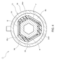
- FIG. 2 shows a cross-sectional view taken along line AOB in FIG. 1 .
- FIGS. 3 and 4 respectively show cross-sectional views taken along lines CD and EF in FIG. 2 .
- the housing 12 includes a cylindrical pipe portion 18 , a first lid portion 20 that covers one end of the pipe portion 18 , and a second lid portion 22 that covers another end of the pipe portion 18 .
- the housing 12 is formed of, for example, metal such as iron or aluminum, or an insulator such as ceramic. Although in this example the housing 12 has a cylindrical shape, the housing 12 may have a different polygonal column shape.
- An outer conductor pipe 24 and an inner conductor pipe 26 are arranged within the housing 12 to share the same axis with the pipe portion 18 .
- the outer conductor pipe 24 and the inner conductor pipe 26 have a hexagonal column shape, and are arranged such that the side surfaces are parallel to each other.
- An insulating layer 28 is provided between the outer conductor pipe 24 and the inner conductor pipe 26 .
- a material having high withstand voltage and high thermal conductivity is used, such as aluminum nitride, aluminum oxide, or mica.
- the right end of the outer conductor pipe 24 is covered by an outer conductor plate 30
- the right end of the inner conductor pipe 26 is covered by an inner conductor plate 31 .
- the right side of the inner conductor pipe 26 is located within the outer conductor pipe 24 , and a remaining portion of the inner conductor pipe 26 projects to the left side from an opening 24 a of the outer conductor pipe 24 .
- the remaining portion is a projecting portion 26 b .
- the switching elements are arranged at predetermined positions near the openings 24 a , 26 a of the outer conductor pipe 24 and the inner conductor pipe 26 , and a greater thickness is provided in an outward direction near the openings 24 a , 26 a of the outer conductor pipe 24 and the inner conductor pipe 26 than in other portions.
- the positive electrode conductor P pierces the second lid portion 22 of the housing 12 , and is joined to the outer conductor plate 30 .
- the positive electrode conductor P and the second lid portion 22 are electrically insulated from each other.
- an insulator material is provided between the positive electrode conductor P and the second lid portion 22 .
- the negative electrode conductor N pierces the second lid portion 22 and the outer conductor plate 30 , and is joined to the inner conductor plate 31 .
- the insulating layer 28 is provided between the negative electrode conductor N and the outer conductor pipe 24 , and between the negative electrode conductor N and the second lid portion 22 .
- the negative electrode conductor N and the second lid portion 22 may directly contact each other.
- first switching elements 32 U, 32 V, and 32 W are arranged on every other side surface of the hexagonal column shape (three side surfaces that are not adjacent to each other) of a portion of the outer conductor pipe 24 that forms a double-layer structure in conjunction with the inner conductor pipe 26 .
- this hexagonal column shape is a regular hexagonal column shape
- the first switching elements 32 U, 32 V, and 32 W are arranged at intervals of 120°.
- Each first switching element is plate-shaped, and has flat terminals on both plate surfaces.
- a control line 34 extends from a side surface of each first switching element.
- each first switching element faces a side surface of the outer conductor pipe 24 , and is attached to the side surface of the outer conductor pipe 24 .
- the terminal of each first switching element that is located closer to the outer conductor pipe 24 is electrically connected to the side surface of the outer conductor pipe 24 by soldering or another method.
- the first switching elements 32 U, 32 V, and 32 W for example, an insulated gate bipolar transistor (IGBT) is used.
- IGBT insulated gate bipolar transistor
- the plate surface on which a collector terminal is provided faces the outer conductor pipe 24
- the plate surface on which an emitter terminal is provided faces opposite the outer conductor pipe 24 side.
- second switching elements 36 U, 36 V, and 36 W are arranged on every other side surface of the hexagonal column shape of the inner conductor pipe 26 .
- this hexagonal column shape is a regular hexagonal column shape
- the second switching elements 36 U, 36 V, and 36 W are arranged at intervals of 120°.
- Each second switching element is plate-shaped, and has flat terminals on both plate surfaces.
- a control line 34 extends from a side surface of each second switching element.
- One of the plate surfaces of each second switching element faces a side surface of the inner conductor pipe 26 , and is attached to the side surface of the inner conductor pipe 26 .
- the terminal of each second switching element that is located closer to the inner conductor pipe 26 is electrically connected to the side surface of the inner conductor pipe 26 by soldering or another method.
- the plate surface on which an emitter terminal is provided faces the inner conductor pipe 26
- the plate surface on which a collector terminal is provided faces opposite the inner conductor pipe 26 side.
- the U phase first switching element 32 U and the U phase second switching element 36 U are aligned in a longitudinal direction of the outer conductor pipe 24 and the inner conductor pipe 26 .
- the V phase first switching element 32 V and the V phase second switching element 36 V are also aligned in the longitudinal direction of the outer conductor pipe 24 and the inner conductor pipe 26
- the W phase first switching element 32 W and the W phase second switching element 36 W are also aligned in the longitudinal direction of the outer conductor pipe 24 and the inner conductor pipe 26 .
- the plate surfaces of the first switching elements 32 U, 32 V, and 32 W that face the inside direction of the conductor pipes 24 and 26 are referred to as inner surfaces, and the plate surfaces on the opposite side are referred to as outer surfaces.
- the plate surfaces of the second switching elements 36 U, 36 V, and 36 W that face the inside direction of the conductor pipes 24 and 26 are referred to as inner surfaces, and the plate surfaces on the opposite side are referred to as outer surfaces.
- the U phase conductor is attached to the outer surfaces of the U phase first switching element 32 U and the U phase second switching element 36 U.
- the U phase first switching element 32 U is interposed between the U phase conductor and the outer conductor pipe 24
- the U phase second switching element 36 U is interposed between the U phase conductor and the projecting portion of the inner conductor pipe 26 .
- the U phase conductor is electrically connected to the terminals provided on the outer surfaces of the U phase first switching element 320 and the U phase second switching element 36 U by soldering or another method.
- the V phase conductor is attached to the outer surfaces of the V phase first switching element 32 V and the V phase second switching element 36 V.
- the V phase first switching element 32 V is interposed between the V phase conductor and the outer conductor pipe 24
- the V phase second switching element 36 V is interposed between the V phase conductor and the projecting portion of the inner conductor pipe 26 .
- the V phase conductor is electrically connected to the terminals provided on the outer surfaces of the V phase first switching element 32 V and the V phase second switching element 36 V by soldering or another method.
- the W phase conductor is attached to the outer surfaces of the W phase first switching element 32 W and the W phase second switching element 36 W.
- the W phase first switching element 32 W is interposed between the W phase conductor and the outer conductor pipe 24
- the W phase second switching element 36 W is interposed between the W phase conductor and the projecting portion of the inner conductor pipe 26 .
- the W phase conductor is electrically connected to the terminals provided on the outer surfaces of the W phase first switching element 32 W and the W phase second switching element 36 W by soldering or another method.
- the U phase conductor, the V phase conductor, and the W phase conductor are elongated in the left direction, and pierce the first lid portion 20 to extend to the outside of the housing 12 .
- the first lid portion 20 is formed of a conductive material, the phase conductors and the first lid portion 20 are electrically insulated from each other. In this case, an insulator material is provided between the phase conductors and the first lid portion 20 .
- the control lines 34 for the first switching elements 32 U, 32 V, and 32 W and the second switching elements 36 U, 36 V, and 36 W are elongated in the right direction, and pierce the second lid portion 22 to extend to the outside of the housing 12 .
- the control lines 34 and the second lid portion 22 are electrically insulated from each other. In this case, an insulator material is provided between the control lines 34 and the second lid portion 22 .
- the outer conductor pipe 24 , the inner conductor pipe 26 , the insulating layer 28 , the first switching elements 32 U, 32 V, and 32 W, the second switching elements 36 U, 36 V, and 36 W, and the phase conductors are molded by a molding resin 38 , and integrated as a molded body 48 .
- a molding resin 38 a heat-resistant and thermally conductive material such as an epoxy resin is used.
- the thickness of a right end portion of the side wall of the pipe portion 18 is increased in an inward direction to reduce the inner diameter.
- the molded body 48 is attached to the housing 12 at a portion in which the inner diameter in the right end of the pipe portion 18 is reduced. Further, a coolant flow channel 46 through which a coolant flows is formed in a region between the molded body 48 and the housing 12 .
- FIG. 5 shows a circuit diagram of an inverter included in the cooling-type switching element module 1 .
- the inverter includes switching element pairs 40 U, 40 V, and 40 W respectively corresponding to the U phase conductor, the V phase conductor, and the W phase conductor.
- the U phase switching element pair 40 U is a pair consisting of the U phase first switching element 32 U and the U phase second switching element 36 U
- the V phase switching element pair 40 V is a pair consisting of the V phase first switching element 32 V and the V phase second switching element 36 V
- the W phase switching element pair 40 W is a pair consisting of the W phase first switching element 32 W and the W phase second switching element 36 W.
- Each of the first switching elements 32 U, 32 V, and 32 W has one end connected to the positive electrode conductor P, and has another end connected to respective one end of each of the second switching elements 36 U, 36 V, and 36 W that pair with the first switching elements 32 U, 32 V, and 32 W. Another end of each of the second switching elements 36 U, 36 V, and 36 W is connected to the negative electrode conductor N.
- the U phase conductor, the V phase conductor, and the W phase conductor are respectively connected to connection nodes between the first switching elements 32 U, 32 V, and 32 W and the second switching elements 36 U, 36 V, and 36 W of the corresponding switching element pairs.
- the circuit is configured such that a terminal on the upper side of each switching element is a collector terminal, and a terminal on the lower side of each switching element is an emitter terminal.
- the control lines 34 are respectively connected to gate terminals of the first switching elements 32 U, 32 V, and 32 W and the second switching elements 36 U, 36 V, and 36 W.
- a direct current voltage corresponding to direct current electric power transmitted by the positive electrode conductor P and the negative electrode conductor N is converted into a three-phase alternating current voltage through switching operations of the switching element pairs 40 U, 40 V, and 40 W.
- the U phase voltage, the V phase voltage, and the W phase voltage are respectively output to the U phase conductor, the V phase conductor, and the W phase conductor.
- the U phase conductor, the V phase conductor, and the W phase conductor transmit three-phase alternating current electric power corresponding to the three-phase alternating current voltage.
- each switching element includes a rectifying element
- the three-phase alternating current voltage corresponding to the three-phase alternating current electric power transmitted by the U phase conductor, the V phase conductor, and the W phase conductor is converted into a direct current voltage through the rectification of the switching elements.
- the positive electrode conductor P and the negative electrode conductor N transmit direct current electric power corresponding to the direct current voltage.
- a structure for causing a coolant to flow will be described below with reference to FIG. 2 .
- the coolant for example, a fluorine-based liquid such as Fluorinert®, or water may be used. Also, a gas may be used as the coolant.
- an electrically conductive coolant may be used.
- An inlet tube 42 is inserted through the side surface of the housing 12 .
- the inlet tube 42 pierces the side wall of the pipe portion 18 , the coolant flow channel 46 , the molding resin 38 , the side wall of the outer conductor pipe 24 , and the side wall of the inner conductor pipe 26 , and communicates with the inside of the inner conductor pipe 26 .
- an outlet tube 44 is inserted through the side surface of the housing 12 , and communicates with the coolant flow channel 46 .
- One end of the inlet tube 42 that is present outside the housing 12 forms the coolant inlet 14
- one end of the outlet tube 44 that is present outside the housing 12 forms the coolant outlet 16 .
- the coolant that has entered through the coolant inlet 14 passes through the inlet tube 42 , and reaches the inside of the inner conductor pipe 26 .
- the coolant passes through the inside of the inner conductor pipe 26 while absorbing heat from the first switching elements 32 U, 32 V, and 32 W and the second switching elements 36 U, 36 V, and 36 W of the switching element pairs 40 U, 40 V, and 40 W, and reaches the coolant flow channel 46 through the inner conductor pipe 26 .
- the coolant passes through the coolant flow channel 46 that is present between the first lid portion 20 and the molded body 48 , and reaches the coolant flow channel 46 that is present between the pipe portion 18 and the molded body 48 .
- the coolant passes through the coolant flow channel 46 that is present between the pipe portion 18 and the molded body 48 while absorbing heat from the second switching elements 36 U, 36 V, and 36 W and the first switching elements 32 U, 32 V, and 32 W of the switching element pairs 40 U, 40 V, and 40 W, and then passes through the outlet tube 44 to be emitted through the coolant outlet 16 .
- the coolant may flow in the reverse direction.
- a voltage applied to the positive electrode conductor P and the negative electrode conductor N is applied to the switching element pairs 40 U, 40 V, and 40 W via the outer conductor pipe 24 and the inner conductor pipe 26 .
- the outer conductor pipe 24 and the inner conductor pipe 26 are opposed to each other in close proximity with the insulating layer 28 being interposed therebetween over a large area.
- the capacitance between the outer conductor pipe 24 and the inner conductor pipe 26 is increased, and respective inductance components are decreased. This prevents a surge voltage from occurring in the inverter.
- the lengths of the current paths from the positive electrode conductor P and the negative electrode conductor N to the switching element pairs 40 U, 40 V, and 40 W for the respective phases are uniform for the respective phases. This reduces variations in electric constants (such as parasitic inductances, parasitic capacitances, or loss resistances) between the phases, and prevents the nonuniformity of phase voltages and phase currents.
- first switching elements 32 U, 32 V, and 32 W and the second switching elements 36 U, 36 V, and 36 W of the switching element pairs 40 U, 40 V, and 40 W are cooled from both sides by the coolant flowing within the inner conductor pipe 26 , and by the coolant flowing through the coolant flow channel 46 . This reduces thermal resistance with respect to the same rate of coolant flow, and enhances the cooling effect.
- the switching element pairs for the respective phases are arranged along the circumferential direction of the outer conductor pipe 24 and the inner conductor pipe 26 . This prevents variations in cooling performance between the phases.
- the feature of arranging the switching elements 32 U, 32 V, 32 W, 36 U, 36 V, and 36 W on the outer conductor pipe 24 and the inner conductor pipe 26 which transmit direct current electric power, and through which a coolant flows eliminates wasted space, and downsizes the cooling-type switching element module. Also, because the structure for electric power transmission and cooling is integrated within the housing 12 , the number of components and the costs are reduced.
- FIG. 6 shows a cross-sectional view of a cooling-type switching element module taken along a plane perpendicular to the longitudinal direction.
- FIG. 7 shows a cross-sectional view taken along line GH in FIG. 6 .
- FIG. 6 is a cross-sectional view taken along line gh in FIG. 7 .
- Components identical to those shown in FIGS. 1 to 5 are denoted by the same reference numerals, and their descriptions are not repeated here.
- the coolant flow channel is branched into narrow channels, and the branch coolant flow channels 46 U, 46 V, and 46 W are provided at positions corresponding to the switching element pairs 40 U, 40 V, and 40 W.
- the structure of the coolant flow channel 46 in a coolant flow zone 50 - 1 and a coolant flow zone 50 - 3 in FIG. 7 is similar to that of the coolant flow channel 46 shown in FIG. 2 .
- the coolant passes through the coolant flow channels 46 U, 46 V, and 46 W, absorbs heat from the switching elements 32 U, 32 V, 32 W, 36 U, 36 V, and 36 W of the switching element pairs 40 U, 40 V, and 40 W, joins into one in the coolant flow zone 50 - 3 , and then passes through the outlet tube 44 to be emitted through the coolant outlet 16 . It should be noted that the coolant may flow in the reverse direction.
- FIG. 8 shows a cooling-type switching element module 3 which is similar to the cooling-type switching element module 2 shown in FIGS. 6 and 7 , and in which the outer conductor pipe 24 and the inner conductor pipe 26 are replaced with those having a nearly triangle column shape.
- This nearly triangle column shape is formed by narrowing the width of every other adjacent side surface of six side surfaces that form a regular hexagonal column shape to make it resemble a triangle column shape.
- the rate of coolant flow is increased compared with the outer conductor pipe 24 and the inner conductor pipe 26 having a hexagonal column shape on the condition that the rate of coolant flow through the coolant inlet 14 and the coolant outlet 16 per unit time is constant, and the cooling performance is enhanced.
- the outer conductor pipe 24 and the inner conductor pipe 26 may be replaced with those having a nearly triangle column shape.
- Hybrid electric vehicles and the like often use a plurality of motor generators.
- Hybrid electric vehicles that are being developed in recent years include, for example, a motor generator for use in electric power generation, and a motor generator for use in driving and regenerative braking.
- An inverter is connected to each of the motor generators.
- FIG. 9 shows a cross-sectional view of two cooling-type switching element modules that are sectioned at an angle as in FIG. 2 .
- Cooling-type switching element modules 1 L and 1 R each have a structure similar to that of the cooling-type switching element module 1 shown in FIGS. 1 to 4 , and are bilaterally symmetrically arranged except for a joint portion 52 .
- Positive electrode conductors P and negative electrode conductors N of the two cooling-type switching element modules 1 L and 1 R are electrically connected in common.
- FIG. 10 shows a top view of the cooling-type switching element modules 1 L and 1 R.
- the negative electrode conductor N that extends in the left direction from the cooling-type switching element module 1 R located on the right side overlaps the negative electrode conductor N that extends in the right direction from the cooling-type switching element module 1 L located on the left side and is terminated, and is elongated in the upward direction in FIG. 10 from the position at which the two negative electrode conductors N overlap each other.
- the positive electrode conductors P and the negative electrode conductors N that extend from the cooling-type switching element modules 1 L and 1 R may overlap each other in the opposite relationship.
- the positive electrode conductor P that extends from the cooling-type switching element module 1 L located on the left side may be configured to be elongated in the upward direction
- the negative electrode conductor N that extends from the cooling-type switching element module 1 L located on the left side may be configured to be elongated in the upward direction
- FIG. 11 shows an enlarged view of the joint portion 52 .
- a positive electrode joint plate 54 L for holding the positive electrode conductor P of the cooling-type switching element module 1 L projects from the second lid portion 22 of the cooling-type switching element module 1 L to extend in the right direction.
- the positive electrode conductor P of the cooling-type switching element module 1 L is located on the upper surface of the positive electrode joint plate 54 L.
- a negative electrode joint plate 56 L for holding the negative electrode conductor N of the cooling-type switching element module 1 L projects from the second lid portion 22 of the cooling-type switching element module 1 L to extend in the right direction.
- the negative electrode conductor N of the cooling-type switching element module 1 L is located on the upper surface of the negative electrode joint plate 56 L.
- a positive electrode joint plate 54 R for holding the positive electrode conductor P of the cooling-type switching element module 1 R projects from the second lid portion 22 of the cooling-type switching element module 1 R to extend in the left direction.
- the positive electrode conductor P of the cooling-type switching element module 1 R is located on the lower surface of the positive electrode joint plate 54 R.
- a negative electrode joint plate 56 R for holding the negative electrode conductor N of the cooling-type switching element module 1 R projects from the second lid portion 22 of the cooling-type switching element module 1 R to extend in the left direction.
- the negative electrode conductor N of the cooling-type switching element module 1 R is located on the lower surface of the negative electrode joint plate 56 R.
- the cooling-type switching element modules 1 L and 1 R are fixed in a position in which the bolt holes of the positive electrode conductors P, the bolt holes of the negative electrode conductors N, the bolt holes of the positive electrode joint plates, and the bolt holes of the negative electrode joint plates match with each other.
- a bolt 58 is inserted into the bolt holes, and the positive electrode joint plates on both sides and the negative electrode joint plates on both sides are joined to each other by means of the bolt 58 and a nut 60 .
- the bolt 58 is formed of a conductive material, the bolt 58 is insulated from the positive electrode conductors P, and the bolt 58 is insulated from the negative electrode conductors N.
- FIGS. 12 and 13 shows a cross-sectional view of a cooling-type switching element module 4 taken along a plane perpendicular to the longitudinal direction.
- FIG. 14 shows a cross-sectional view taken along line IOJ in FIG. 12 .
- FIG. 12 is a cross-sectional view taken along line KM in FIG. 14
- FIG. 13 is a cross-sectional view taken along line QR in FIG. 14 .
- Components identical to those shown in FIGS. 1 to 5 are denoted by the same reference numerals, and their descriptions are not repeated here.
- the outer conductor pipe 24 is extended from a position in which an opening 26 a of the inner conductor pipe 26 is located.
- the first switching elements 32 U, 32 V, and 32 W are provided inside the extension portion 24 b of the outer conductor pipe 24
- the second switching elements 36 U, 36 V, and 36 W are provided inside the inner conductor pipe 26 .
- the outer conductor pipe 24 and the inner conductor pipe 26 are arranged within the housing 12 to share the same axis with the pipe portion 18 .
- the outer conductor pipe 24 and the inner conductor pipe 26 have a hexagonal column shape, and are arranged such that the side surfaces are parallel to each other.
- An insulating layer 28 is provided between the outer conductor pipe 24 and the inner conductor pipe 26 .
- the inner conductor pipe 26 is located inside the outer conductor pipe 24 , and the outer conductor pipe 24 has a extension portion 24 b extending from the position at which the opening 26 a of the inner conductor pipe 26 is located.
- the first switching elements 32 U, 32 V, and 32 W are arranged on every other side surface of the hexagonal column shape inside the extension portion of the outer conductor pipe 24 .
- One of the plate surfaces of each first switching element faces a side surface of the outer conductor pipe 24 , and is attached to the side surface of the outer conductor pipe 24 .
- the terminal of each first switching element that is located closer to the outer conductor pipe 24 is electrically connected to the side surface of the outer conductor pipe 24 by soldering or another method.
- the plate surface on which a collector terminal is provided faces the outer conductor pipe 24
- the plate surface on which an emitter terminal is provided faces opposite the outer conductor pipe 24 side.
- the second switching elements 36 U, 36 V, and 36 W are arranged on every other side surface of the hexagonal column shape inside the portion of the inner conductor pipe 26 that forms a double-layer structure in conjunction with the outer conductor pipe 24 .
- One of the plate surfaces of each second switching element 36 U, 36 V, or 36 W faces a side surface of the inner conductor pipe 26 , and is attached to the side surface of the inner conductor pipe 26 .
- the terminal of each second switching element that is located closer to the inner conductor pipe 26 is electrically connected to the side surface of the inner conductor pipe 26 by soldering or another method.
- the plate surface on which an emitter terminal is provided faces the inner conductor pipe 26
- the plate surface on which a collector terminal is provided faces opposite the inner conductor pipe 26 side.
- the thicknesses of the U phase conductor, the V phase conductor, and the W phase conductor are increased in an outward direction in portions that are attached to the respectively corresponding first switching elements 32 U, 32 V, and 32 W and the respectively corresponding second switching elements 36 U, 36 V, and 36 W.
- Each of the first switching elements 32 U, 32 V, and 32 W and the second switching elements 36 U, 36 V, and 36 W in the respective phases has an inner surface to which one of the phase conductors corresponding to the respective phases is attached.
- the first switching elements 32 Y, 32 V, and 32 W are interposed between one of the phase conductors and the extension portion of the outer conductor pipe 24
- the second switching elements 36 U, 36 V, and 36 W are interposed between one of the phase conductors and the inner conductor pipe 26 .
- the phase conductors are electrically connected to the terminals provided on the inner surfaces of the first switching elements 32 U, 32 V, and 32 W and the second switching elements 36 U, 36 V, and 36 W by soldering or another method.
- the phase conductors are elongated in the left direction, and pierce the first lid portion 20 to extend to the outside of the housing 12 .
- the first lid portion 20 is formed of a conductive material, the phase conductors and the first lid portion 20 are electrically insulated from each other. In this case, an insulator material is provided between the phase conductors and the first lid portion 20 .
- the outer conductor pipe 24 , the inner conductor pipe 26 , the insulating layer 28 , the first switching elements 32 U, 32 V, and 32 W, the second switching elements 36 U, 36 V, and 36 W, and the phase conductors are molded by a molding resin 38 within the outer conductor pipe 24 and the inner conductor pipe 26 , and integrated as a molded body 48 .
- the thickness of a right end portion of the side wall of the pipe portion 18 is increased in an inward direction to reduce the inner diameter.
- the molded body 48 is attached to the housing 12 at a portion in which the inner diameter in the right end of the pipe portion 18 is reduced.
- An inlet tube 42 is inserted through the side surface of the housing 12 .
- the inlet tube 42 pierces the side wall of the pipe portion 18 , the coolant flow channel 46 , the side wall of the outer conductor pipe 24 , the side wall of the inner conductor pipe 26 , and the molding resin 38 , and communicates with the inside of the inner conductor pipe 26 .
- an outlet tube 44 is inserted through the side surface of the housing 12 , and communicates with the coolant flow channel 46 .
- One end of the inlet tube 42 that is present outside the housing 12 forms the coolant inlet 14
- one end of the outlet tube 44 that is present outside the housing 12 forms the coolant outlet 16 .
- the coolant that has entered through the coolant inlet 14 passes through the inlet tube 42 , and reaches the inside of the inner conductor pipe 26 .
- the coolant passes through the inside of the inner conductor pipe 26 and the inside of the extension portion of the outer conductor pipe 24 while absorbing heat from the second switching elements 36 U, 36 V, and 36 W and the first switching elements 32 U, 32 V, and 32 W of the switching element pairs 40 U, 40 V, and 40 W, and reaches the coolant flow channel 46 through the outer conductor pipe 24 .
- the coolant passes through the coolant flow channel 46 that is present between the first lid portion 20 and the molded body 48 , and reaches the coolant flow channel 46 that is present between the pipe portion 18 and the outer conductor pipe 24 .
- the coolant passes through the coolant flow channel 46 that is present between the pipe portion 18 and the molded body 48 while absorbing heat from the first switching elements 32 U, 32 V, and 32 W and the second switching elements 36 U, 36 V, and 36 W of the switching element pairs 40 U, 40 V, and 40 W, and then passes through the outlet tube 44 to be emitted through the coolant outlet 16 .
- the coolant may flow in the reverse direction.
- advantages similar to those of the first embodiment are achieved. More specifically, the advantages achieved not only include advantages of, for example, prevention of a surge voltage from occurring in the inverter and stabilization of the alternating current voltage, but also include advantages of, for example, enhancement in the cooling effect, downsizing of the cooling-type switching element module, and reduction in the number of components and the costs.
- FIGS. 15 and 16 show a cross-sectional view of a cooling-type switching element module 5 taken along a plane perpendicular to the longitudinal direction.
- FIG. 17 shows a cross-sectional view taken along line ST in FIG. 15 .
- FIG. 15 is a cross-sectional view taken along line XX in FIG. 17
- FIG. 16 is a cross-sectional view taken along line ⁇ in FIG. 17 .
- switching elements constituting two inverters are housed in a single housing 12 .
- Components identical to those shown in FIGS. 1 to 5 are denoted by the same reference numerals, and their descriptions are not repeated here.
- first switching elements 32 U- 1 , 32 V- 1 , and 32 W- 1 of a first inverter are arranged on every other side surface (three surfaces that are not adjacent to each other) of a portion of the outer conductor pipe 24 that forms a double-layer structure in conjunction with the inner conductor pipe 26 .
- a first switching element 32 U- 2 of a second inverter is provided on a side surface that is located opposite the side surface on which the first switching element 32 U- 1 of the first inverter is provided.
- a first switching element 32 V- 2 of the second inverter is provided on a side surface that is located opposite the side surface on which the first switching element 32 V- 1 of the first inverter is provided
- a first switching element 32 W- 2 of the second inverter is provided on a side surface that is located opposite the side surface on which the first switching element 32 W- 1 of the first inverter is provided.
- the first switching elements 32 U- 1 , 32 V- 1 , and 32 W- 1 of the first inverter and the first switching elements 32 U- 2 , 32 V- 2 , and 32 W- 2 of the second inverter are arranged at positions rotationally symmetric by 180°.
- the first switching elements of the first inverter and the first switching elements of the second inverter are provided on adjacent side surfaces, and are alternately arranged in the order of 32 U- 1 , 32 W- 2 , 32 V- 1 , 32 U- 2 , 32 W- 1 , and 32 V- 2 in a clockwise direction.
- second switching elements 36 U- 1 , 36 V- 1 , and 36 W- 1 of the first inverter are arranged on every other side surface of the projecting portion of the inner conductor pipe 26 . Further, a second switching element 36 U- 2 of the second inverter is provided on a side surface that is located opposite the side surface on which the second switching element 36 U- 1 of the first inverter is provided.
- a second switching element 36 V- 2 of the second inverter is provided on a side surface that is located opposite the side surface on which the second switching element 36 V- 1 of the first inverter is provided
- a second switching element 36 W- 2 of the second inverter is provided on a side surface that is located opposite the side surface on which the second switching element 36 W- 1 of the first inverter is provided.
- the second switching elements 36 U- 1 , 36 V- 1 , and 36 W- 1 of the first inverter and the second switching elements 36 U- 2 , 36 V- 2 , and 36 W- 2 of the second inverter are arranged at positions rotationally symmetric by 180°.
- the second switching elements of the first inverter and the second switching elements of the second inverter are provided on adjacent side surfaces, and are alternately arranged in the order of 36 U- 1 , 36 W- 2 , 36 V- 1 , 36 U- 2 , 36 W- 1 , and 36 V- 2 in a clockwise direction.
- switching element pairs of the first inverter and the switching element pairs of the second inverter be alternately arranged along the perimeter of the outer conductor pipe 24 and the inner conductor pipe, but the order of arrangement may be changed in accordance with the design.
- a U phase conductor U 1 , a V phase conductor V 1 , and a W phase conductor W 1 of the first inverter are elongated in the left direction, and pierce the first lid portion 20 to extend to the outside of the housing 12 .
- the first lid portion 20 is formed of a conductive material, the phase conductors of the first inverter and the first lid portion 20 are electrically insulated from each other. In this case, an insulator material is provided between the phase conductors of the first inverter and the first lid portion 20 .
- a U phase conductor U 2 , a V phase conductor V 2 , and a W phase conductor W 2 of the second inverter are elongated in the right direction, and pierce the second lid portion 22 to extend to the outside of the housing 12 .
- the second lid portion 22 is formed of a conductive material, the phase conductors of the second inverter and the second lid portion 22 are electrically insulated from each other. In this case, an insulator material is provided between the phase conductors of the second inverter and the second lid portion 22 .
- three-phase conductors extend from both ends of the housing 12 .
- the positive electrode conductor P and the negative electrode conductor N are therefore inserted into the housing 12 by means of a structure as will be described below.
- the positive electrode conductor P pierces the pipe portion 18 and the molding resin 38 , and is joined to the outer conductor pipe 24 .
- the pipe portion 18 is formed of a conductive material
- the positive electrode conductor P and the pipe portion 18 are electrically insulated from each other.
- an insulator material is provided between the positive electrode conductor P and the pipe portion 18 .
- the negative electrode conductor N pierces the pipe portion 18 , the molding resin 38 , and the outer conductor pipe 24 , and is joined to the inner conductor pipe 26 .
- the pipe portion 18 When the pipe portion 18 is formed of a conductive material, the negative electrode conductor N and the pipe portion 18 are electrically insulated from each other. In this case, an insulator material is provided between the negative electrode conductor N and the pipe portion 18 . Further, an insulator material is provided between the negative electrode conductor N and the outer conductor pipe 24 , and the negative electrode conductor N and the outer conductor pipe 24 are electrically insulated from each other.
- inverters are housed.
- the present invention can be employed in a step-up/step-down converter that steps up or steps down a direct current voltage, or other electric power conversion circuits including switching element pairs.
- the present invention may be employed not only in an inverter that performs dc-ac conversion between direct current electric power and three-phase alternating current electric power, but also in an inverter that performs dc-ac conversion between direct current electric power and single-phase alternating current electric power, or between direct current electric power and polyphase alternating current electric power having four or more phases.
- fins for increasing the heat transfer area may be provided on the wall surface of the channel through which the coolant flows in the cooling-type switching element module.
- turbulence of the flow of the coolant or boiling of the coolant may be caused by, for example, forming a projection, a groove, or the like on the wall surface of the channel through which the coolant flows, or applying porous surface treatment. This is because turbulence of the flow of the coolant or boiling of the coolant can in some cases improve the cooling performance.
- each of the positive electrode conductor P, the negative electrode conductor N, the U phase conductor, the V phase conductor, and the W phase conductor is formed of a metal strip.
- These conductors may have a circular or a polygonal cross section other than hexagonal.
Abstract
Description
Claims (10)
Applications Claiming Priority (2)
| Application Number | Priority Date | Filing Date | Title |
|---|---|---|---|
| JP2013-003121 | 2013-01-11 | ||
| JP2013003121A JP5726215B2 (en) | 2013-01-11 | 2013-01-11 | Cooling type switching element module |
Publications (2)
| Publication Number | Publication Date |
|---|---|
| US20140198449A1 US20140198449A1 (en) | 2014-07-17 |
| US9198332B2 true US9198332B2 (en) | 2015-11-24 |
Family
ID=51164956
Family Applications (1)
| Application Number | Title | Priority Date | Filing Date |
|---|---|---|---|
| US14/145,451 Active 2034-07-03 US9198332B2 (en) | 2013-01-11 | 2013-12-31 | Cooling-type switching element module |
Country Status (2)
| Country | Link |
|---|---|
| US (1) | US9198332B2 (en) |
| JP (1) | JP5726215B2 (en) |
Cited By (3)
| Publication number | Priority date | Publication date | Assignee | Title |
|---|---|---|---|---|
| US10593609B2 (en) * | 2017-04-04 | 2020-03-17 | Toyota Jidosha Kabushiki Kaisha | Semiconductor device and power converter |
| US10985088B2 (en) * | 2016-05-24 | 2021-04-20 | Mitsubishi Electric Corporation | System comprising at least one power module comprising at least one power die that is cooled by liquid cooled system |
| US20220142012A1 (en) * | 2020-10-29 | 2022-05-05 | Ford Global Technologies, Llc | Liquid cooled terminal block assemblies |
Families Citing this family (10)
| Publication number | Priority date | Publication date | Assignee | Title |
|---|---|---|---|---|
| JP5694278B2 (en) * | 2012-11-21 | 2015-04-01 | 三菱電機株式会社 | Power converter |
| JP6156283B2 (en) * | 2014-08-07 | 2017-07-05 | 株式会社デンソー | Power converter |
| JP6166743B2 (en) * | 2015-02-20 | 2017-07-19 | 本田技研工業株式会社 | Power converter |
| ITUB20153344A1 (en) * | 2015-09-02 | 2017-03-02 | St Microelectronics Srl | ELECTRONIC POWER MODULE WITH IMPROVED THERMAL DISSIPATION AND ITS MANUFACTURING METHOD |
| US11013143B2 (en) * | 2016-11-12 | 2021-05-18 | Exascaler Inc. | Electronic device for liquid immersion cooling, power supply unit, and cooling system |
| WO2018206106A1 (en) * | 2017-05-10 | 2018-11-15 | Preh Gmbh | Casing for housing electronic components |
| FR3078448B1 (en) * | 2018-02-27 | 2020-02-28 | Institut Vedecom | BUS ASSEMBLY FORMING A HOUSING AND A THERMAL DISSIPATOR FOR AN ELECTRONIC POWER DEVICE |
| FR3111048A1 (en) * | 2020-05-26 | 2021-12-03 | Thales | Inverter device |
| US20220352137A1 (en) * | 2020-11-02 | 2022-11-03 | Dynex Semiconductor Limited | High power density 3d semiconductor module packaging |
| DE102021213427B3 (en) | 2021-11-29 | 2023-05-25 | Zf Friedrichshafen Ag | COMPACT POWER INVERTER MODULE |
Citations (20)
| Publication number | Priority date | Publication date | Assignee | Title |
|---|---|---|---|---|
| JP2000049281A (en) | 1998-07-31 | 2000-02-18 | Toshiba Corp | Semiconductor device |
| JP2001128467A (en) | 1999-10-27 | 2001-05-11 | Hitachi Ltd | Power conversion device |
| US6255672B1 (en) | 1997-11-26 | 2001-07-03 | Kabushiki Kaisha Toshiba | Semiconductor device |
| US20010033477A1 (en) | 2000-04-19 | 2001-10-25 | Seiji Inoue | Coolant cooled type semiconductor device |
| JP2002026215A (en) | 2000-06-30 | 2002-01-25 | Denso Corp | Cooling fluid cooling type semiconductor device |
| US20040189114A1 (en) | 2003-03-25 | 2004-09-30 | Nissan Motor Co., Ltd. | Power converter and related method |
| JP2004297847A (en) | 2003-03-25 | 2004-10-21 | Nissan Motor Co Ltd | Power convertor |
| JP2007116840A (en) | 2005-10-21 | 2007-05-10 | Nichicon Corp | Inverter module and inverter-integrated alternating current motor using the same |
| US7249929B2 (en) * | 2003-11-13 | 2007-07-31 | United Technologies Corporation | Bleed housing |
| JP2007335530A (en) | 2006-06-13 | 2007-12-27 | Toyota Motor Corp | Semiconductor module and semiconductor device |
| JP2008311496A (en) | 2007-06-15 | 2008-12-25 | Toyota Motor Corp | Cooling structure of semiconductor device |
| US7671382B2 (en) * | 2005-12-19 | 2010-03-02 | Mitsubishi Electric Corporation | Semiconductor device with thermoplastic resin to reduce warpage |
| US7687901B2 (en) * | 2005-01-24 | 2010-03-30 | Toyota Jidosha Kabushiki Kaisha | Heat dissipating fins opposite semiconductor elements |
| US7965508B2 (en) * | 2007-03-27 | 2011-06-21 | Denso Corporation | Cooling device for electronic component and power converter equipped with the same |
| JP2012239256A (en) | 2011-05-10 | 2012-12-06 | Denso Corp | Electric power conversion apparatus |
| US8363402B2 (en) * | 2007-09-17 | 2013-01-29 | International Business Machines Corporation | Integrated circuit stack |
| US8390131B2 (en) * | 2004-06-03 | 2013-03-05 | International Rectifier Corporation | Semiconductor device with reduced contact resistance |
| US8462529B2 (en) * | 2007-07-30 | 2013-06-11 | GM Global Technology Operations LLC | Power converter assembly with symmetrical layout of power modules |
| US8952525B2 (en) * | 2011-03-04 | 2015-02-10 | Hitachi Automotive Systems, Ltd. | Semiconductor module and method for manufacturing semiconductor module |
| US9072197B2 (en) * | 2011-03-10 | 2015-06-30 | Toyota Jidosha Kabushiki Kaisha | Cooling apparatus |
Family Cites Families (3)
| Publication number | Priority date | Publication date | Assignee | Title |
|---|---|---|---|---|
| DE19846156C1 (en) * | 1998-10-07 | 2000-07-27 | Bosch Gmbh Robert | Arrangement of a multi-phase converter |
| JP5241688B2 (en) * | 2009-11-13 | 2013-07-17 | 日立オートモティブシステムズ株式会社 | Power converter |
| JP5423811B2 (en) * | 2010-01-08 | 2014-02-19 | トヨタ自動車株式会社 | Semiconductor module |
-
2013
- 2013-01-11 JP JP2013003121A patent/JP5726215B2/en active Active
- 2013-12-31 US US14/145,451 patent/US9198332B2/en active Active
Patent Citations (22)
| Publication number | Priority date | Publication date | Assignee | Title |
|---|---|---|---|---|
| US6255672B1 (en) | 1997-11-26 | 2001-07-03 | Kabushiki Kaisha Toshiba | Semiconductor device |
| JP2000049281A (en) | 1998-07-31 | 2000-02-18 | Toshiba Corp | Semiconductor device |
| JP2001128467A (en) | 1999-10-27 | 2001-05-11 | Hitachi Ltd | Power conversion device |
| US20010033477A1 (en) | 2000-04-19 | 2001-10-25 | Seiji Inoue | Coolant cooled type semiconductor device |
| JP2002026215A (en) | 2000-06-30 | 2002-01-25 | Denso Corp | Cooling fluid cooling type semiconductor device |
| JP2004297846A (en) | 2003-03-25 | 2004-10-21 | Nissan Motor Co Ltd | Power convertor |
| JP2004297847A (en) | 2003-03-25 | 2004-10-21 | Nissan Motor Co Ltd | Power convertor |
| US20040189114A1 (en) | 2003-03-25 | 2004-09-30 | Nissan Motor Co., Ltd. | Power converter and related method |
| US7249929B2 (en) * | 2003-11-13 | 2007-07-31 | United Technologies Corporation | Bleed housing |
| US8390131B2 (en) * | 2004-06-03 | 2013-03-05 | International Rectifier Corporation | Semiconductor device with reduced contact resistance |
| US7687901B2 (en) * | 2005-01-24 | 2010-03-30 | Toyota Jidosha Kabushiki Kaisha | Heat dissipating fins opposite semiconductor elements |
| JP2007116840A (en) | 2005-10-21 | 2007-05-10 | Nichicon Corp | Inverter module and inverter-integrated alternating current motor using the same |
| US7671382B2 (en) * | 2005-12-19 | 2010-03-02 | Mitsubishi Electric Corporation | Semiconductor device with thermoplastic resin to reduce warpage |
| JP2007335530A (en) | 2006-06-13 | 2007-12-27 | Toyota Motor Corp | Semiconductor module and semiconductor device |
| US7965508B2 (en) * | 2007-03-27 | 2011-06-21 | Denso Corporation | Cooling device for electronic component and power converter equipped with the same |
| US20100182747A1 (en) | 2007-06-15 | 2010-07-22 | Toyota Jidosha Kabuishiki Kaisha | Semiconductor element cooling structure |
| JP2008311496A (en) | 2007-06-15 | 2008-12-25 | Toyota Motor Corp | Cooling structure of semiconductor device |
| US8462529B2 (en) * | 2007-07-30 | 2013-06-11 | GM Global Technology Operations LLC | Power converter assembly with symmetrical layout of power modules |
| US8363402B2 (en) * | 2007-09-17 | 2013-01-29 | International Business Machines Corporation | Integrated circuit stack |
| US8952525B2 (en) * | 2011-03-04 | 2015-02-10 | Hitachi Automotive Systems, Ltd. | Semiconductor module and method for manufacturing semiconductor module |
| US9072197B2 (en) * | 2011-03-10 | 2015-06-30 | Toyota Jidosha Kabushiki Kaisha | Cooling apparatus |
| JP2012239256A (en) | 2011-05-10 | 2012-12-06 | Denso Corp | Electric power conversion apparatus |
Cited By (4)
| Publication number | Priority date | Publication date | Assignee | Title |
|---|---|---|---|---|
| US10985088B2 (en) * | 2016-05-24 | 2021-04-20 | Mitsubishi Electric Corporation | System comprising at least one power module comprising at least one power die that is cooled by liquid cooled system |
| US10593609B2 (en) * | 2017-04-04 | 2020-03-17 | Toyota Jidosha Kabushiki Kaisha | Semiconductor device and power converter |
| US20220142012A1 (en) * | 2020-10-29 | 2022-05-05 | Ford Global Technologies, Llc | Liquid cooled terminal block assemblies |
| US11622479B2 (en) * | 2020-10-29 | 2023-04-04 | Ford Global Technologies, Llc | Liquid cooled terminal block assemblies |
Also Published As
| Publication number | Publication date |
|---|---|
| JP5726215B2 (en) | 2015-05-27 |
| JP2014135410A (en) | 2014-07-24 |
| US20140198449A1 (en) | 2014-07-17 |
Similar Documents
| Publication | Publication Date | Title |
|---|---|---|
| US9198332B2 (en) | Cooling-type switching element module | |
| US10319665B2 (en) | Cooler and cooler fixing method | |
| JP5447453B2 (en) | Switching module | |
| US7957135B2 (en) | Semiconductor module | |
| JP4719187B2 (en) | Semiconductor device cooling structure | |
| JP5544255B2 (en) | Semiconductor power module and power converter | |
| WO2012108048A1 (en) | Power conversion device | |
| CN103782380A (en) | Semiconductor module | |
| WO2007080922A1 (en) | Semiconductor power converter | |
| JP2012129309A (en) | Switching module | |
| JP6286541B2 (en) | Power module device and power conversion device | |
| JP4055042B2 (en) | Inverter device | |
| JP7139603B2 (en) | power converter | |
| JP2012005191A (en) | Power conversion apparatus | |
| JP2007180155A (en) | Condenser device | |
| JP6134798B2 (en) | Power converter | |
| US11222879B2 (en) | Semiconductor module structure | |
| JP6318668B2 (en) | Semiconductor device | |
| JPWO2019043886A1 (en) | Power converter | |
| JP7233510B1 (en) | power converter | |
| US20230395457A1 (en) | Power Semiconductor Device, Power Conversion Device, and Electric System | |
| JP2002209391A (en) | Semiconductor power converter | |
| WO2023092442A1 (en) | Integrated power semiconductor apparatus | |
| JP7074028B2 (en) | Power converter | |
| WO2021015050A1 (en) | Electric circuit device |
Legal Events
| Date | Code | Title | Description |
|---|---|---|---|
| AS | Assignment |
Owner name: TOYOTA JIDOSHA KABUSHIKI KAISHA, JAPAN Free format text: ASSIGNMENT OF ASSIGNORS INTEREST;ASSIGNORS:OSADA, HIROSHI;USUI, MASANORI;SUGIYAMA, TAKAHIDE;AND OTHERS;REEL/FRAME:031864/0135 Effective date: 20131213 |
|
| STCF | Information on status: patent grant |
Free format text: PATENTED CASE |
|
| MAFP | Maintenance fee payment |
Free format text: PAYMENT OF MAINTENANCE FEE, 4TH YEAR, LARGE ENTITY (ORIGINAL EVENT CODE: M1551); ENTITY STATUS OF PATENT OWNER: LARGE ENTITY Year of fee payment: 4 |
|
| AS | Assignment |
Owner name: DENSO CORPORATION, JAPAN Free format text: ASSIGNMENT OF ASSIGNORS INTEREST;ASSIGNOR:TOYOTA JIDOSHA KABUSHIKI KAISHA;REEL/FRAME:052285/0419 Effective date: 20191224 |
|
| AS | Assignment |
Owner name: DENSO CORPORATION, JAPAN Free format text: ASSIGNMENT OF ASSIGNORS INTEREST;ASSIGNOR:TOYOTA JIDOSHA KABUSHIKI KAISHA;REEL/FRAME:053727/0319 Effective date: 20200630 |
|
| MAFP | Maintenance fee payment |
Free format text: PAYMENT OF MAINTENANCE FEE, 8TH YEAR, LARGE ENTITY (ORIGINAL EVENT CODE: M1552); ENTITY STATUS OF PATENT OWNER: LARGE ENTITY Year of fee payment: 8 |