US9190440B2 - Image sensor and method for fabricating the same - Google Patents
Image sensor and method for fabricating the same Download PDFInfo
- Publication number
- US9190440B2 US9190440B2 US14/300,948 US201414300948A US9190440B2 US 9190440 B2 US9190440 B2 US 9190440B2 US 201414300948 A US201414300948 A US 201414300948A US 9190440 B2 US9190440 B2 US 9190440B2
- Authority
- US
- United States
- Prior art keywords
- image sensor
- region
- trench
- layer
- substrate
- Prior art date
- Legal status (The legal status is an assumption and is not a legal conclusion. Google has not performed a legal analysis and makes no representation as to the accuracy of the status listed.)
- Active
Links
- 238000000034 method Methods 0.000 title description 26
- 239000000758 substrate Substances 0.000 claims abstract description 76
- 230000004888 barrier function Effects 0.000 claims abstract description 68
- 238000009792 diffusion process Methods 0.000 claims abstract description 54
- 238000007667 floating Methods 0.000 claims abstract description 54
- 238000012546 transfer Methods 0.000 claims abstract description 39
- 238000006243 chemical reaction Methods 0.000 claims abstract description 35
- 238000009413 insulation Methods 0.000 claims description 28
- 239000000463 material Substances 0.000 claims description 13
- 230000000295 complement effect Effects 0.000 claims description 5
- 239000010410 layer Substances 0.000 description 159
- 239000012535 impurity Substances 0.000 description 21
- 230000008569 process Effects 0.000 description 17
- 238000002955 isolation Methods 0.000 description 12
- 238000012545 processing Methods 0.000 description 12
- 238000005530 etching Methods 0.000 description 11
- 230000002596 correlated effect Effects 0.000 description 10
- 238000010586 diagram Methods 0.000 description 10
- 238000005070 sampling Methods 0.000 description 9
- VYPSYNLAJGMNEJ-UHFFFAOYSA-N Silicium dioxide Chemical compound O=[Si]=O VYPSYNLAJGMNEJ-UHFFFAOYSA-N 0.000 description 8
- XUIMIQQOPSSXEZ-UHFFFAOYSA-N Silicon Chemical compound [Si] XUIMIQQOPSSXEZ-UHFFFAOYSA-N 0.000 description 6
- 239000011229 interlayer Substances 0.000 description 6
- 229910052710 silicon Inorganic materials 0.000 description 6
- 239000010703 silicon Substances 0.000 description 6
- 230000006866 deterioration Effects 0.000 description 5
- 230000007274 generation of a signal involved in cell-cell signaling Effects 0.000 description 5
- 230000015654 memory Effects 0.000 description 5
- 239000004065 semiconductor Substances 0.000 description 5
- 238000010521 absorption reaction Methods 0.000 description 4
- 238000004891 communication Methods 0.000 description 4
- 230000007547 defect Effects 0.000 description 4
- 229910052814 silicon oxide Inorganic materials 0.000 description 4
- 229910052581 Si3N4 Inorganic materials 0.000 description 3
- 230000000875 corresponding effect Effects 0.000 description 3
- 239000013078 crystal Substances 0.000 description 3
- 238000005286 illumination Methods 0.000 description 3
- 238000004519 manufacturing process Methods 0.000 description 3
- 229910021421 monocrystalline silicon Inorganic materials 0.000 description 3
- 150000004767 nitrides Chemical class 0.000 description 3
- 229910021420 polycrystalline silicon Inorganic materials 0.000 description 3
- 238000002203 pretreatment Methods 0.000 description 3
- 229910052681 coesite Inorganic materials 0.000 description 2
- 230000001276 controlling effect Effects 0.000 description 2
- 230000008878 coupling Effects 0.000 description 2
- 238000010168 coupling process Methods 0.000 description 2
- 238000005859 coupling reaction Methods 0.000 description 2
- 229910052906 cristobalite Inorganic materials 0.000 description 2
- 238000013461 design Methods 0.000 description 2
- 238000005468 ion implantation Methods 0.000 description 2
- 238000010295 mobile communication Methods 0.000 description 2
- 230000009467 reduction Effects 0.000 description 2
- 239000000377 silicon dioxide Substances 0.000 description 2
- HQVNEWCFYHHQES-UHFFFAOYSA-N silicon nitride Chemical compound N12[Si]34N5[Si]62N3[Si]51N64 HQVNEWCFYHHQES-UHFFFAOYSA-N 0.000 description 2
- 239000002356 single layer Substances 0.000 description 2
- 229910052682 stishovite Inorganic materials 0.000 description 2
- 230000007704 transition Effects 0.000 description 2
- 229910052905 tridymite Inorganic materials 0.000 description 2
- 230000015572 biosynthetic process Effects 0.000 description 1
- 230000000903 blocking effect Effects 0.000 description 1
- 238000013500 data storage Methods 0.000 description 1
- 230000000694 effects Effects 0.000 description 1
- 238000005516 engineering process Methods 0.000 description 1
- 238000010438 heat treatment Methods 0.000 description 1
- 238000011065 in-situ storage Methods 0.000 description 1
- 230000010354 integration Effects 0.000 description 1
- 238000005224 laser annealing Methods 0.000 description 1
- 239000011159 matrix material Substances 0.000 description 1
- 239000007769 metal material Substances 0.000 description 1
- 238000012986 modification Methods 0.000 description 1
- 230000004048 modification Effects 0.000 description 1
- 230000003287 optical effect Effects 0.000 description 1
- 230000003647 oxidation Effects 0.000 description 1
- 238000007254 oxidation reaction Methods 0.000 description 1
- 238000005498 polishing Methods 0.000 description 1
- 230000004044 response Effects 0.000 description 1
- 229920006395 saturated elastomer Polymers 0.000 description 1
- 230000035945 sensitivity Effects 0.000 description 1
- 239000000126 substance Substances 0.000 description 1
- 238000001039 wet etching Methods 0.000 description 1
Images


Classifications
-
- H—ELECTRICITY
- H01—ELECTRIC ELEMENTS
- H01L—SEMICONDUCTOR DEVICES NOT COVERED BY CLASS H10
- H01L27/00—Devices consisting of a plurality of semiconductor or other solid-state components formed in or on a common substrate
- H01L27/14—Devices consisting of a plurality of semiconductor or other solid-state components formed in or on a common substrate including semiconductor components sensitive to infrared radiation, light, electromagnetic radiation of shorter wavelength or corpuscular radiation and specially adapted either for the conversion of the energy of such radiation into electrical energy or for the control of electrical energy by such radiation
- H01L27/144—Devices controlled by radiation
- H01L27/146—Imager structures
- H01L27/14601—Structural or functional details thereof
- H01L27/1462—Coatings
- H01L27/14623—Optical shielding
-
- H—ELECTRICITY
- H01—ELECTRIC ELEMENTS
- H01L—SEMICONDUCTOR DEVICES NOT COVERED BY CLASS H10
- H01L27/00—Devices consisting of a plurality of semiconductor or other solid-state components formed in or on a common substrate
- H01L27/14—Devices consisting of a plurality of semiconductor or other solid-state components formed in or on a common substrate including semiconductor components sensitive to infrared radiation, light, electromagnetic radiation of shorter wavelength or corpuscular radiation and specially adapted either for the conversion of the energy of such radiation into electrical energy or for the control of electrical energy by such radiation
- H01L27/144—Devices controlled by radiation
- H01L27/146—Imager structures
- H01L27/14601—Structural or functional details thereof
- H01L27/14609—Pixel-elements with integrated switching, control, storage or amplification elements
- H01L27/1461—Pixel-elements with integrated switching, control, storage or amplification elements characterised by the photosensitive area
-
- H—ELECTRICITY
- H01—ELECTRIC ELEMENTS
- H01L—SEMICONDUCTOR DEVICES NOT COVERED BY CLASS H10
- H01L27/00—Devices consisting of a plurality of semiconductor or other solid-state components formed in or on a common substrate
- H01L27/14—Devices consisting of a plurality of semiconductor or other solid-state components formed in or on a common substrate including semiconductor components sensitive to infrared radiation, light, electromagnetic radiation of shorter wavelength or corpuscular radiation and specially adapted either for the conversion of the energy of such radiation into electrical energy or for the control of electrical energy by such radiation
- H01L27/144—Devices controlled by radiation
- H01L27/146—Imager structures
- H01L27/14601—Structural or functional details thereof
- H01L27/14609—Pixel-elements with integrated switching, control, storage or amplification elements
- H01L27/14612—Pixel-elements with integrated switching, control, storage or amplification elements involving a transistor
-
- H—ELECTRICITY
- H01—ELECTRIC ELEMENTS
- H01L—SEMICONDUCTOR DEVICES NOT COVERED BY CLASS H10
- H01L27/00—Devices consisting of a plurality of semiconductor or other solid-state components formed in or on a common substrate
- H01L27/14—Devices consisting of a plurality of semiconductor or other solid-state components formed in or on a common substrate including semiconductor components sensitive to infrared radiation, light, electromagnetic radiation of shorter wavelength or corpuscular radiation and specially adapted either for the conversion of the energy of such radiation into electrical energy or for the control of electrical energy by such radiation
- H01L27/144—Devices controlled by radiation
- H01L27/146—Imager structures
- H01L27/14601—Structural or functional details thereof
- H01L27/1464—Back illuminated imager structures
-
- H—ELECTRICITY
- H01—ELECTRIC ELEMENTS
- H01L—SEMICONDUCTOR DEVICES NOT COVERED BY CLASS H10
- H01L27/00—Devices consisting of a plurality of semiconductor or other solid-state components formed in or on a common substrate
- H01L27/14—Devices consisting of a plurality of semiconductor or other solid-state components formed in or on a common substrate including semiconductor components sensitive to infrared radiation, light, electromagnetic radiation of shorter wavelength or corpuscular radiation and specially adapted either for the conversion of the energy of such radiation into electrical energy or for the control of electrical energy by such radiation
- H01L27/144—Devices controlled by radiation
- H01L27/146—Imager structures
- H01L27/14643—Photodiode arrays; MOS imagers
-
- H—ELECTRICITY
- H01—ELECTRIC ELEMENTS
- H01L—SEMICONDUCTOR DEVICES NOT COVERED BY CLASS H10
- H01L29/00—Semiconductor devices adapted for rectifying, amplifying, oscillating or switching, or capacitors or resistors with at least one potential-jump barrier or surface barrier, e.g. PN junction depletion layer or carrier concentration layer; Details of semiconductor bodies or of electrodes thereof ; Multistep manufacturing processes therefor
- H01L29/66—Types of semiconductor device ; Multistep manufacturing processes therefor
- H01L29/68—Types of semiconductor device ; Multistep manufacturing processes therefor controllable by only the electric current supplied, or only the electric potential applied, to an electrode which does not carry the current to be rectified, amplified or switched
- H01L29/76—Unipolar devices, e.g. field effect transistors
- H01L29/762—Charge transfer devices
- H01L29/765—Charge-coupled devices
- H01L29/768—Charge-coupled devices with field effect produced by an insulated gate
- H01L29/76816—Output structures
-
- H—ELECTRICITY
- H01—ELECTRIC ELEMENTS
- H01L—SEMICONDUCTOR DEVICES NOT COVERED BY CLASS H10
- H01L29/00—Semiconductor devices adapted for rectifying, amplifying, oscillating or switching, or capacitors or resistors with at least one potential-jump barrier or surface barrier, e.g. PN junction depletion layer or carrier concentration layer; Details of semiconductor bodies or of electrodes thereof ; Multistep manufacturing processes therefor
- H01L29/66—Types of semiconductor device ; Multistep manufacturing processes therefor
- H01L29/68—Types of semiconductor device ; Multistep manufacturing processes therefor controllable by only the electric current supplied, or only the electric potential applied, to an electrode which does not carry the current to be rectified, amplified or switched
- H01L29/76—Unipolar devices, e.g. field effect transistors
- H01L29/762—Charge transfer devices
- H01L29/765—Charge-coupled devices
- H01L29/768—Charge-coupled devices with field effect produced by an insulated gate
- H01L29/76825—Structures for regeneration, refreshing, leakage compensation or the like
-
- H—ELECTRICITY
- H01—ELECTRIC ELEMENTS
- H01L—SEMICONDUCTOR DEVICES NOT COVERED BY CLASS H10
- H01L27/00—Devices consisting of a plurality of semiconductor or other solid-state components formed in or on a common substrate
- H01L27/14—Devices consisting of a plurality of semiconductor or other solid-state components formed in or on a common substrate including semiconductor components sensitive to infrared radiation, light, electromagnetic radiation of shorter wavelength or corpuscular radiation and specially adapted either for the conversion of the energy of such radiation into electrical energy or for the control of electrical energy by such radiation
- H01L27/144—Devices controlled by radiation
- H01L27/146—Imager structures
- H01L27/14601—Structural or functional details thereof
- H01L27/1462—Coatings
- H01L27/14621—Colour filter arrangements
-
- H—ELECTRICITY
- H01—ELECTRIC ELEMENTS
- H01L—SEMICONDUCTOR DEVICES NOT COVERED BY CLASS H10
- H01L27/00—Devices consisting of a plurality of semiconductor or other solid-state components formed in or on a common substrate
- H01L27/14—Devices consisting of a plurality of semiconductor or other solid-state components formed in or on a common substrate including semiconductor components sensitive to infrared radiation, light, electromagnetic radiation of shorter wavelength or corpuscular radiation and specially adapted either for the conversion of the energy of such radiation into electrical energy or for the control of electrical energy by such radiation
- H01L27/144—Devices controlled by radiation
- H01L27/146—Imager structures
- H01L27/14601—Structural or functional details thereof
- H01L27/14625—Optical elements or arrangements associated with the device
- H01L27/14627—Microlenses
Definitions
- Exemplary embodiments of the present invention relate to a semiconductor design technology, and more particularly, to an image sensor and a method for fabricating the same.
- An image sensor is a semiconductor element which changes a photonic image into an electrical signal.
- Image sensors generally include a plurality of pixels that are arranged in the shape of a two-dimensional matrix. Each of the pixels contains a photoelectric conversion region that generates a photo-charge in response to incident light and uses the photo-charge outputs to output a pixel signal.
- Exemplary embodiments of the present invention are directed to an image sensor and a method for fabricating the same.
- Exemplary embodiments of the present invention may prevent generation of photo-charges which cause noise in the floating diffusion region by forming the floating diffusion region with a barrier layer. Reduction in the signal to noise ratio relative to prior art results in improved image sensor characteristics.
- an image sensor may include a transfer gate formed on a front-side of a substrate, a photoelectric conversion region formed on a side of the transfer gate, a floating diffusion region including a trench formed on the other side of the transfer gate a barrier layer, which covers a bottom of the trench, and a conducting layer, which is gap-filled in the trench.
- the barrier layer may cover the bottom plane of the trench and a portion of the side plane of the trench.
- the barrier layer may include an insulation layer, which absorbs or reflects incident light.
- the barrier layer may include a single insulation layer or a stacked layer having a plurality of insulation layers with different refractive indexes.
- the barrier layer may include a stacked layer where a first insulation layer and a second insulation layer having different refractive indexes are alternately stacked.
- the conducting layer and the substrate may be composed of the same material.
- the conducting layer may include a first region of a first conductive type and a second region of second conductive type, which vertically overlap, and wherein the first conductive type and the second conductive type are complementary.
- the first region and the second region may be electrically coupled to the substrate.
- the image sensor may further include a color filter formed on a back-side of the substrate, and a micro lens formed on the color filter.
- an image sensor may include a transfer gate formed on a front-side of a substrate, a photoelectric conversion region formed on a side of the transfer gate, a floating diffusion region including a trench, which is formed in the other side of the transfer gate, a barrier layer, which covers a bottom of the trench, and a conducting layer, which is gap-filled in the trench, and a trap region formed under the trench.
- the trap region may be electrically separated from the conducting layer by the barrier layer.
- a ground voltage may be provided to the trap region.
- the barrier layer may cover a bottom plane of the trench and a portion of a side of the trench.
- the barrier layer may include an insulation layer, which absorbs or reflects incident light.
- the conducting layer and the substrate may be composed of the same material.
- the conducting layer may include a first region of a first conductive type and a second region of a second conductive type, which overlap vertically, and wherein the first conductive type and the second conductive type are complementary.
- the first region and the second region may be electrically coupled to the substrate.
- the image sensor may further include a color filter formed on a back-side of the substrate, and a micro lens formed on the color filter.
- a method for fabricating an image sensor may include forming a trench by selectively etching a substrate, forming a barrier layer which covers a bottom plane of the trench, forming a floating diffusion region including the trench, the barrier layer and a conducting layer by forming the conducting layer, which is gap-filled in the trench, forming a photoelectric conversion region in the substrate, and forming a transfer gate on the substrate such that the photoelectric conversion region and the floating diffusion region are disposed on a side of the substrate and the other side of the substrate.
- the forming of the barrier may include forming the barrier layer along a surface of a structure including the trench, forming a sacrificial layer, which is partially gap-filled in the trench, etching the barrier layer exposed by the sacrificial layer, and removing the sacrificial layer.
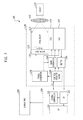
- FIG. 1 is an equivalent circuit diagram illustrating an image sensor in accordance with an exemplary embodiment of the present invention.
- FIG. 2 is a plane diagram illustrating a pixel of an image sensor in accordance with an exemplary embodiment of the present invention.
- FIG. 3 is a cross sectional view taken along A-A′ of FIG. 2 in accordance with an exemplary embodiment of the present invention.
- FIG. 4 is a cross sectional view taken along A-A′ of FIG. 2 in accordance with an exemplary embodiment of the present invention.
- FIGS. 5A and 5B are cross sectional views taken along A-A′ of FIG. 2 in accordance with an exemplary embodiment of the present invention.
- FIGS. 6A to 6E are cross sectional views illustrating a method for fabricating an image sensor in accordance with an exemplary embodiment of the present invention.
- FIG. 7 is a block diagram illustrating an image processing system in accordance with an exemplary embodiment of the present invention.
- FIG. 8 is a detailed block diagram illustrating an image sensor shown in FIG. 7 .
- FIG. 9 is a block diagram illustrating an image processing system in accordance with an exemplary embodiment of the present invention.
- ‘and/or’ represents that one or more of components arranged before and after ‘and/or’ is included.
- “connected/coupled” refers to one component not only directly coupling another component but also indirectly coupling another component through an intermediate component.
- a singular form may include a plural form (and vice versa) as long as it is not specifically mentioned.
- ‘include/comprise’ or ‘including/comprising’ used in the specification represents that one or more components, steps, operations, and elements exist or are added.
- Image sensors are classified into charge coupled device (CCD) image sensors and a CMOS image sensors. CMOS image sensors are further classified into front-side illumination (FSI) image sensors and back-side illumination (BSI) image sensors.
- FSI front-side illumination
- BSI back-side illumination
- the BSI image sensor has excellent operation characteristics, low manufacturing cost, and high manufacturing yield compared to other image sensors such as CCD image sensors or FSI image sensors.
- BSI image sensors have concerns regarding noise and signal deterioration caused by high signal to noise ratios.
- T will be a first conductive type and a second conductive type, which are complementary.
- the first conductive type is a P-type
- the second conductive type is an N-type.
- the first conductive type is an N-type
- the second conductive type is a P-type.
- Embodiments of the present invention include an image sensor and an image sensor fabrication method where characteristic deterioration is prevented by reducing the signal to noise ratio relative to the conventional art.
- the reduction in signal to noise ratio is accomplished by preventing unwanted photo-charges from being generated in regions other than the photoelectric conversion region.
- signal noise may result from un-wanted photo-charges being generated in a floating diffusion region (FD).
- FD floating diffusion region
- FIG. 1 is an equivalent circuit diagram illustrating an image sensor in accordance with an exemplary embodiment of the present invention.
- FIG. 2 is a plane diagram illustrating a pixel of an image sensor in accordance with an exemplary embodiment of the present invention.
- FIG. 3 is a cross sectional view taken along A-A′ of FIG. 2 in accordance with an exemplary embodiment of the present invention.
- a pixel of an imager sensor may include a photoelectric conversion region PD, a transfer transistor Tx, a drive transistor Dx, a reset transistor Rx, and a selection transistor Sx.
- the photoelectric conversion region PD may include a plurality of photoelectric conversion units, which are vertically overlapped. Each of the plurality of photoelectric conversion units may be a photo diode including an N-type impurity region 120 and a P-type impurity region 130 .
- a transfer gate of the transfer transistor Tx may be extended to the inside of the substrate.
- the transfer gate may include a recess gate, a saddle-fin gate, or a buried gate.
- a drain of the transfer transistor Tx may be a floating diffusion region M.
- the floating diffusion region FD may be a source of the reset transistor Rx.
- the floating diffusion region FD may be electrically coupled to a drive gate of the drive transistor Dx.
- the drive transistor Dx and the reset transistor Rx may be coupled in series.
- the drive transistor Dx may be coupled to the selection transistor Sx.
- the reset transistor Rx, the drive transistor Dx, and the selection transistor Sx may be shared among neighboring pixels, which may improve integration.
- an element isolation layer 110 may be formed on a substrate 100 .
- a gate of the transfer transistor Tx and a gate of the reset transistor Rx may be formed on the substrate 100 .
- the photoelectric conversion region PD may be formed on a side of the substrate 100 .
- the floating diffusion region FD may be formed on the other side of the substrate 100 .
- the photoelectric conversion region PD and the floating diffusion region FD may be formed by ion-implanting impurities on the substrate 100 .
- An interlayer insulation layer 140 including a signal generation circuit, may be formed on a front-side FS of the substrate 100 .
- a color filter 150 and a micro leas 160 may be formed on a back-side BS of the substrate 100 .
- a back-side illumination (BSI) image sensor may increase the light-reception area by illuminating light on a back-side of the substrate 100 .
- wavelengths with large absorption depth bandwidth e.g. a wavelength of red or green bandwidth
- a wavelength of large absorption depth bandwidth may reach the floating diffusion region FD and generate a photo-charge.
- the intended area to generate a photo-charge is the photoelectric conversion region PD.
- the charge is accumulated in the floating diffusion region FD and serves to produce a pixel signal.
- Photo-charges generated in the floating diffusion region FD act as a noise source in the pixel signal and deteriorate the image sensor characteristics. This is especially true when the photoelectric conversion region PD is saturated with photo-charges from a strong light source. This results in an increased signal to noise ratio and deterioration of image sensor characteristics due to photo-charges being generated in the floating diffusion region FD.
- Exemplary embodiments of the present invention may provide an image sensor and a method for fabricating the same that prevents unwanted photo-charges from being generated in the floating diffusion region FD.
- FIG. 4 is a cross sectional view taken along A-A′ of FIG. 2 in accordance with an exemplary embodiment of the present invention.
- an image sensor in accordance with an exemplary embodiment of the present invention may include a substrate 100 , an element isolation layer 110 , a transfer gate of a transfer transistor Tx, a reset gate of a reset transistor Rx, a photoelectric conversion region PD, a floating diffusion region FD, an interlayer insulation layer 140 , a color filter 150 , and a micro lens 160 .
- the substrate 100 may include a first conductive type semiconductor substrate.
- the semiconductor substrate may be in a single crystal state and include a silicon-containing material.
- the substrate 100 may be a bulk silicon substrate or a silicon layer isolated from a handle wafer.
- the element isolation layer 110 may be formed on the front-side FS of the substrate 100 .
- the element isolation layer 110 may be formed by a shallow trench isolation process and may include an insulation layer.
- a bottom plane of the element isolation layer may be extended to contact with a back-side BS of the substrate 100 .
- the transfer gate of the transfer transistor Tx and a reset gate of the reset transistor Rx may be formed on the substrate 100 .
- the photoelectric conversion region PD is formed on a side of the transfer gate of the transfer transistor Tx.
- the photoelectric conversion region PD may include at least one photoelectric conversion unit, which is vertically overlapped.
- the photoelectric conversion unit(s) may be a photo diode including a first impurity region 120 of a first conductive type, e.g., P-type impurity region, and a second conductive impurity region 130 of a second conductive type, e.g., N-type impurity region.
- the first impurity region 120 may have a thickness smaller than the thickness of the second impurity region and may contact the front-side FS of the substrate 100 .
- the second impurity region 130 may be separated from the back-side BS of the substrate 100 or be in contact with the back-side BS of the substrate 100 .
- the floating diffusion region FD may be formed on the other side of the substrate 100 .
- the floating diffusion region FD may include a trench 210 , which is formed in the transfer gate of the transfer transistor Tx; a barrier layer 220 , which covers a bottom plane of the trench 210 ; and a conducting layer 230 , which is gap-filled in the trench 210 .
- the trench 210 may be formed by etching the substrate 100 in an area corresponding to the floating diffusion region. From the front-side FS of the substrate, the trench 210 may have a depth corresponding to that of the floating diffusion region FD and may be formed through an impurity ion-implantation process.
- the barrier layer 220 prevents light from the back-side BS of the substrate from reaching the floating diffusion region FD.
- the barrier layer 220 covers the bottom plane of the trench 210 to efficiently block light coming from the back-side BS of the substrate 100 .
- the barrier layer 220 may be extended to the sides of the trench 210 . That is, the barrier layer 220 may cover a bottom plane and a side plane(s) of the trench 210 . If the barrier layer 220 is extended to the side plane of the trench 210 , the barrier layer 220 may be separated from the front-side FS of the substrate 100 to provide a current path between the photoelectric conversion region PD and the floating diffusion region FD, and between the floating diffusion region FD and a channel region of the reset transistor Rx.
- the barrier layer 220 may block light from reaching the floating diffusion region FD by absorption or reflection using an insulation layer.
- a metallic material it is not recommended to use a metallic material as the barrier layer 220 since unwanted photo-charges may be generated by light incident: on an interface between the barrier layer 220 and the substrate 100 or between the barrier layer 220 and the conducting layer 230 .
- the barrier layer 220 may include a single insulation layer selected from a group comprised of an oxide layer, a nitride layer, and an oxynitride layer, or a stacked layer where two or more of the just mentioned insulation layers are stacked. If the barrier layer 220 has a stacked insulation layer, the stacked insulation layer may be composed of a plurality of insulation layers having different refractive indexes to adjust the absorption rate or reflexibility of incident light. If the barrier layer 220 is a single insulation layer, the barrier layer 220 may be a silicon oxide layer SiO 2 . If the barrier layer 220 is the stacked layer, a silicon oxide layer SiO 2 and a silicon nitride layer Si 3 N 4 may be alternately stacked once or more.
- Light reflected from the barrier layer 220 falls on the photoelectric conversion region PD or exits to the outside. Although an unwanted photo-charge may be generated by light reflected from the barrier layer 220 , the probability is low and the effect on signal noise is generally negligible for photo-charges that are generated outside of the floating diffusion region FD.
- the conducting layer 230 which is gap-filled in the trench 210 , may have a second conductive type, and may operate as a drain of the transfer transistor Tx and a source of the reset transistor Rx.
- the conducting layer 230 may be contacted with the substrate 100 where no barrier layer 220 is present. That is, the conducting layer 230 may be electrically coupled to the substrate 100 .
- the conducting layer 230 may include the same material as the substrate 100 .
- the conducting layer 230 may include a silicon-containing material, a poly-silicon layer, or a single crystal silicon layer.
- the interlayer insulation layer 140 is formed on the front-side FS of the substrate 100 and includes a signal generation circuit.
- the interlayer insulation layer 140 may be comprised of a single layer or two stacked layers selected from a group comprised of an oxide layer, a nitride layer, and an oxynitride layer.
- the signal generation circuit formed within the interlayer insulation layer 140 may include a plurality of transistors, metallic lines of a multi-layer (not shown), and a contact plug (not shown), which couples them to each other.
- the signal generation circuit may generate a pixel signal corresponding to a photo-charge generated in the photoelectric conversion region PD.
- the plurality of transistors may include the transfer transistors Tx, the reset transistor Rx, the drive transistor Dx, and the selection transistor Sx.
- the color filter 150 may be formed on the back-side BS of the substrate 100 .
- the micro lens 160 may be formed on the color filter 150 .
- the aforementioned image sensor in accordance with the exemplary embodiment of the present invention may prevent unwanted photo-charges from being generated by having a floating diffusion region FD with a barrier layer 220 that blocks light from reaching the floating diffusion region FD.
- the image sensor may prevent deterioration of characteristics caused by an increase in signal to noise ratio, particularly when a strong light source is present.
- FIGS. 5A and 5B An image sensor in accordance with another exemplary embodiment of the present invention will now be described with reference to FIGS. 5A and 5B .
- FIGS. 5A and 5B For conveniently describing the embodiment, a detailed description of previously mentioned and common elements will be omitted.
- FIGS. 5A and 5B are cross sectional views taken along the A-A′ plane of FIG. 2 .
- the conducting layer 230 which is gap-filled in the trench 210 may include a first region 232 having a first conductive type and a second region 234 having a second conductive type, which vertically overlap.
- the first region 232 and the second region 234 may contact the substrate 100 where the barrier layer 220 is not formed. That is, the first region 232 and the second region 234 may be electrically coupled to the substrate 100 .
- the first region 232 may prevent the generation of dark current.
- the first region 232 may contacted the front-side FS of the substrate 100 , a bottom plane of the trench 210 , or a side plane of the trench 210 .
- the second region 234 may operate as a drain of the transfer transistor Tx and a source of the reset transistor Rx.
- the second region 234 may be disposed under the first region 232 or above the first region 232 . That is, the first region 232 may be in contact with the front-side FS of the substrate 100 .
- the second region 234 may be disposed under the first region 232 , or the first region 232 may be disposed under the second region 234 .
- the conducting layer 230 may prevent unwanted photo-charges from being generated in the floating diffusion region FD, reduce dark current, and improve image sensor characteristics.
- a trap region 250 may be formed under the floating diffusion region FD.
- the trap region 250 may remove the dark current from the surface of the trench 210 and may remove unwanted photo-charges generated by the light reflected from the barrier layer 220 .
- the trap region 250 may be an impurity region, which is formed by ion-implanting an impurity of the first conductive type on the substrate 100 .
- the trap region 250 may be electrically separated from the conducting layer 230 by the barrier layer 220 to prevent the generation of photo-charges caused by a junction between the trap region 250 and the conducting region 230 .
- the trap region 250 may be grounded.
- the trap region 250 prevents the unwanted photo-charges from being generated in the floating diffusion region FD, which improves image sensor characteristics and reduces dark current. Additionally, the signal to noise ratio may be reduced by removing the unwanted photo-charges generated by light reflected from the barrier layer 220 .
- FIGS. 6A to 6E are cross sectional views illustrating a method for fabricating an image sensor in accordance with an exemplary embodiment of the present invention. A method for fabricating the image sensor shown in FIG. 4 will now be described.
- a substrate 10 having a first conductive type is prepared.
- the semiconductor substrate may be in a single crystal state and may include a silicon-containing material.
- an element isolation layer 12 may be formed in the substrate 10 .
- the element isolation layer 12 may be formed through a shallow trench isolation (STI) process. That is, the element isolation layer 12 may be formed by first producing an element isolation trench via selectively etching the substrate 10 . An insulation layer may then be gap-filled in the element isolation trench,
- STI shallow trench isolation
- a trench 14 may be formed by etching the substrate 14 in an area that will be the floating diffusion region FD.
- the trench 14 may be formed using an etching process to provide space for forming the floating diffusion region FD.
- a barrier layer 16 may be formed along a surface of the substrate 10 , including the trench 14 .
- the barrier layer 16 may prevent photo-charges from being generated in the floating diffusion region FD and block light from reaching the floating diffusion region FD.
- the barrier layer 16 may include a material such as an insulation layer which absorbs or reflects the incident light.
- the barrier layer 16 may include a single layer or a stacked layer of two or more materials selected from a group comprised of an oxide layer, a nitride layer, and an oxynitride layer.
- the barrier layer 16 may be formed of a silicon oxide layer or at least two stacked layers where a silicon oxide layer and a silicon nitride layer are alternately stacked.
- a pre-treatment process for curing surface defects of the trench 14 may be performed prior to formation of the barrier layer 16 .
- the pre-treatment process may use an anneal process, e.g. a fast heat treatment or a laser anneal. Further, the pre-treatment process may cure surface defects of the trench 14 by forming a sacrificial layer on the surface of the structure, including the trench 14 , through thermal oxidation followed by removal of the sacrificial layer. For reference, surface defects of the trench 14 may operate as a source of a dark current.
- a bottom plane of the trench 14 may be covered by selectively etching the barrier layer 16 .
- the portion of the barrier layer which is etched to cover the bottom plane of the trench 14 will now be referred to as ‘ 16 A’.
- the barrier layer 16 A By etching the barrier layer 16 A to cover the bottom of the trench 14 , the incident light is prevented from reaching the floating diffusion region FD, a current path is provided between the photoelectric conversion region PD and the floating diffusion region FD, and between a channel region of the reset transistor Rx and the floating diffusion region FD.
- the barrier layer 16 A covers the bottom of the trench 14 and may be extended to the side(s) of the trench 14 .
- An etching process for the barrier layer 16 A may be accomplished by forming a sacrificial layer (not shown) to bury part of the trench 14 in the barrier layer 16 A, etching an exposed barrier layer 16 A, and removing the sacrificial layer.
- the etching process may be performed through a wet etching process to prevent substrate defects from occurring.
- a conducting layer 18 of a second conducting type is gap-filled in the trench 14 .
- a conducting layer 18 gap-fill process may be accomplished by forming the conducting layer 18 to cover the entire surface of the substrate 10 , including the trench 14 , and performing a planarization process, e.g., a chemical mechanical polishing (CMP) until the surface of the substrate 10 is exposed.
- CMP chemical mechanical polishing
- an impurity of the second conducting type may be implanted in situ, or the impurity of the second conducting type may be ion-implanted after the second conducting layer 18 is formed.
- the conducting layer 18 and the substrate 10 may be composed of the same material. More specifically, the conducting layer 18 may include a silicon-containing material. That is, the conducting layer 18 may include a poly-silicon layer or a single crystal silicon layer. The single crystal silicon layer may be formed through an epitaxial growth manner by using a seed as the surface of the trench 14 on which the barrier layer 16 A is not formed.
- the floating diffusion region FD including the trench 14 , the barrier layer 16 A, and the conducting layer 18 may be formed.
- the barrier layer 16 A may cover at least the bottom of the trench 14 and the conducting layer 18 may be gap-filled in the trench 14 .
- a post-treatment may be performed to improve interface characteristics of the junction between the substrate 10 and the conducting layer 18 .
- the post-treatment may be performed through a laser annealing process.
- the photoelectric conversion region PD may be formed in the substrate 10 .
- the photoelectric conversion region PD may have a first impurity region 20 of a first conducting type and a second impurity type region 22 of a second conducting type, which vertically overlap each other.
- the first impurity region 20 and the second impurity region 22 may be formed through an ion-implantation process.
- the transfer transistor Tx may be formed such that the photoelectric conversion region PD and the floating diffusion region FD are disposed on different sides of the substrate 10 . Further, an interlayer insulation layer 24 including a signal generation circuit of the reset transistor Rx, the drive transistor Dx, the selection transistor Sx, metallic lines of a multi-layer, and a plurality of contact plugs, may be formed.
- a color filter 26 may be formed on a back-side BS of the substrate 10 , and a micro lens 28 may be formed on the color filter 26 .
- an image sensor may be completed by using a published fabricating process.
- FIG. 7 is a block diagram illustrating an image processing system in accordance with an exemplary embodiment of the present invention.
- the image processing system 1000 may include an image sensor 1100 , a digital signal processor (DSP) 1200 , a display unit 1300 and a lens module 1500 .
- DSP digital signal processor
- the image sensor 1100 may include a pixel array 1110 , a row driver 1120 , a correlated double sampling (CDS) block 1130 , an analogue to digital converter (ADC) 1140 , a ramp signal generator 1160 , a timing generator 1170 , a control register 1180 and a buffer 1190 .
- CDS correlated double sampling
- ADC an analogue to digital converter
- the pixel array 1110 may include the above-described floating diffusion region FD in accordance with an exemplary embodiment of the present invention. More specifically, each of the plurality of pixels of the pixel array 1110 may include the floating diffusion region FD, which includes the transfer gate formed on the substrate, the photoelectric conversion region PD formed on a side of the transfer gate, the trench formed on the other side of the transfer gate, the barrier layer covering a bottom plane of the trench, and the conducting layer, which is gap-filled in the trench.
- the above-described floating diffusion region FD blocks unwanted photo-charges from being generated by blocking light from reaching the floating diffusion region FD. Thus, the characteristics of the image sensor may be improved by reducing the signal to noise ratio.
- the image sensor 1100 may detect an optical image of an object 1400 photographed by the lens module 1500 under the control of the digital signal processor (DSP) 1200 .
- the digital signal processor (DSP) 1200 may output to the display unit 1300 an image detected and outputted by the image sensor 1100 .
- the display unit 1300 may represent a device capable of displaying the image outputted from the digital signal processor (DSP) 1200 .
- the display unit 1300 may be a terminal of a computer, a mobile communication apparatus, or another image display apparatus.
- the digital signal processor (DSP) 1200 may include a camera controller 1201 , an image signal processor (ISP) 1203 and an interface (I/F) 1205 .
- the camera controller 1201 may control operation of the control resistor 1180 .
- the camera controller 1201 may control operation of the image sensor 1100 or the control register 1180 by using an inter-integrated circuit I 2 C.
- the image signal processor (ISP) 1203 may receive an image or image data, process the received image and output the processed image through the interface (I/F) 1205 to the display unit 1300 .
- FIG. 7 shows that the image signal processor (ISP) 1203 is included in the digital signal processor (DSP) 1200 .
- the image signal processor (ISP) 1203 may be disposed in the image sensor 1100 according to system design.
- the image sensor 1100 and the image signal processor (ISP) 1203 may be put together in a package, for example as a multi-chip package (MCP).
- MCP multi-chip package
- FIG. 8 is a detailed block diagram illustrating an image sensor shown in FIG. 7 .
- the timing generator 1170 may generate one or more control signals for controlling each of the row driver 1120 , the correlated double sampling (CDS) block 1130 , the analogue to digital converter (ADC) 1140 , and the ramp signal generator 1150 .
- the control register 1180 may generate one or more control signals for controlling the ramp signal generator 1160 , the timing generator 1170 , and the buffer 1190 .
- the control register 1180 may be controlled by the camera controller 1201 .
- the row driver 1120 may drive the pixel array by a row as a unit. For example, the row driver 1120 may generate a selection signal for selecting one of the plurality of rows.
- Each of the plurality of rows may include a plurality of pixels.
- FIG. 8 shows a simplified disposition of the plurality of pixels for a clearer description.
- the plurality of pixels may include the pixel array described above.
- the plurality of pixels may detect incident light and output an image reset signal and an image signal to the correlated double sampling (CDS) block 1130 .
- the pixel array in accordance with the present invention may prevent generation of dark current and deterioration of sensitivity due to the charge trap region. This may provide a good quality pixel signal, image reset signal, and image signal.
- the correlated double sampling (CDS) block 1130 may perform a correlated double sampling on each of the received image reset signals and the image signals.
- the analogue to digital converter (ADC) 1140 may compare a ramp signal outputted from the ramp signal generator 1160 and the correlated double sampled signal outputted from the correlated double sampling (CDS) block 1130 to output a comparison result signal, count transition time of the comparison result signal, and output the counted value to the buffer 1190 .
- ADC analogue to digital converter
- the analogue to digital converter (ADC) 1140 may include a comparing block 1145 and a counter block 1150 .
- the comparing block 1145 may include a plurality of comparators 1149 .
- Each of the plurality of comparators 1149 may be connected to the correlated double sampling (CDS) block 1130 and the ramp signal generator 1160 .
- the plurality of output signals from the correlated double sampling (CDS) block 1130 may be inputted to a first terminal, for example a negative terminal, of the respective comparators 1149 and the ramp signal from the ramp signal generator 1160 may be inputted to a second terminal, for example a positive terminal, of each of the comparators 1149 .
- the plurality of comparators 1149 may receive and compare the respective output signals from the correlated double sampling (CDS) block 1130 and the ramp signal from the ramp signal generator 1160 and output the comparison result signals.
- a comparison result signal outputted from a first comparator 1149 for comparing an output signal from one of the plurality of pixels and the ramp signal from the ramp signal generator 1160 , may correspond to a difference between the image signal and the image reset signal that varies depending on the amount of light received.
- the ramp signal generator 1160 may operate under the control of the timing generator 1170 .
- the counter block 1150 may include a plurality of counters 1151 .
- the plurality of counters 1151 may be connected to respective output terminals of the plurality of comparators 1149 .
- the counter block 1150 may count the transition time of the comparison result signal using a clock signal CNT_CLK outputted from the timing generator 1170 and output a digital signal or the counted value to the buffer 1190 .
- the counter block 1150 may output a plurality of digital image signals.
- Each of the counters 1151 may be an up/down counter or a bit-wise inversion counter.
- the buffer 1190 may store, sense, amplify, and output the plurality of digital image signals outputted from the analogue to digital converter (ADC) 1140 .
- the buffer 1190 may include a memory block 1191 and a sense amplifier 1192 .
- the memory block 1191 may include a plurality of memories 1193 storing the respective counted value outputted from the plurality counters 1151 .
- the counted value may represent a counted value with respect to a signal outputted from the plurality of pixels.
- the sense amplifier 1192 may sense and amplify each of the counted values outputted from the memory block 1191 .
- the image sensor 1100 may output the image data to the digital signal processor (DSP) 1200 .
- DSP digital signal processor
- FIG. 9 is a block diagram illustrating an image processing system including an image sensor in accordance with an embodiment of the present invention.
- the image processing system 2000 may be a data processing apparatus using or supporting mobile industry processor interfaces (MIPI) such as a mobile communication apparatus, a personal digital assistant (PDA), a mobile phone, or a smart phone.
- MIPI mobile industry processor interfaces
- the image processing system 2000 may be a portable apparatus such as a tablet computer.
- the image processing system 2000 may include an application processor 2010 an image sensor 2040 , and a display 2050 .
- a camera serial interface (CSI) host 2012 in the application processor 2010 may perform serial communication with the CSI device 2041 of the image sensor 2040 through a camera serial interface (CSI).
- the image sensor 2040 may include the image sensor in accordance with an embodiment of the present invention.
- a display serial interface (DSI) host 2011 may perform serial communication with the DSI device 2051 of the display 2050 through a display serial interface (DSI).
- the image processing system 2000 may further include a radio frequency (RF) chip 2060 capable of performing communication with the application processor 2010 .
- RF radio frequency
- a physical layer (PHY) 2013 of the application processor 2010 and a physical layer (PHY) 2061 of the radio frequency (RF) chip 2060 may exchange data according to mobile industry processor interface (MPI) digital radio frequency (DigRF),
- MPI mobile industry processor interface
- the image processing system 2000 may further include a geographic positioning system (GPS) 2020 , a data storage device 2070 , a memory 2085 such as dynamic random access memory (DRAM), and a speaker 2090 .
- the image processing system 2000 may perform communication through a worldwide interoperability for microwave access (Wimax) unit 2030 , a wireless local area network (WLAN) unit 2100 and an ultra-wideband (UWB) unit 2110 .
- Wimax worldwide interoperability for microwave access
- WLAN wireless local area network
- UWB ultra-wideband
Applications Claiming Priority (2)
| Application Number | Priority Date | Filing Date | Title |
|---|---|---|---|
| KR10-2013-0158162 | 2013-12-18 | ||
| KR1020130158162A KR20150071768A (ko) | 2013-12-18 | 2013-12-18 | 이미지 센서 및 그 제조방법 |
Publications (2)
| Publication Number | Publication Date |
|---|---|
| US20150171133A1 US20150171133A1 (en) | 2015-06-18 |
| US9190440B2 true US9190440B2 (en) | 2015-11-17 |
Family
ID=53369486
Family Applications (1)
| Application Number | Title | Priority Date | Filing Date |
|---|---|---|---|
| US14/300,948 Active US9190440B2 (en) | 2013-12-18 | 2014-06-10 | Image sensor and method for fabricating the same |
Country Status (3)
| Country | Link |
|---|---|
| US (1) | US9190440B2 (ko) |
| KR (1) | KR20150071768A (ko) |
| CN (1) | CN104733485B (ko) |
Families Citing this family (28)
| Publication number | Priority date | Publication date | Assignee | Title |
|---|---|---|---|---|
| JP2015095468A (ja) * | 2013-11-08 | 2015-05-18 | ソニー株式会社 | 固体撮像素子および固体撮像素子の製造方法、並びに電子機器 |
| US9443900B2 (en) * | 2014-08-25 | 2016-09-13 | Taiwan Semiconductor Manufacturing Co., Ltd. | Pixel with multigate structure for charge storage or charge transfer |
| US9613916B2 (en) | 2015-03-12 | 2017-04-04 | Taiwan Semiconductor Manufacturing Co., Ltd. | Protection ring for image sensors |
| WO2017112786A1 (en) | 2015-12-21 | 2017-06-29 | Google Inc. | Automatic suggestions for message exchange threads |
| KR102174346B1 (ko) | 2015-12-21 | 2020-11-04 | 구글 엘엘씨 | 메시징 애플리케이션들을 위한 자동적인 제안들 및 다른 콘텐츠 |
| WO2018057536A1 (en) | 2016-09-20 | 2018-03-29 | Google Llc | Bot requesting permission for accessing data |
| WO2018057541A1 (en) | 2016-09-20 | 2018-03-29 | Google Llc | Suggested responses based on message stickers |
| US10015124B2 (en) | 2016-09-20 | 2018-07-03 | Google Llc | Automatic response suggestions based on images received in messaging applications |
| US10416846B2 (en) | 2016-11-12 | 2019-09-17 | Google Llc | Determining graphical element(s) for inclusion in an electronic communication |
| KR102380819B1 (ko) * | 2017-04-12 | 2022-03-31 | 삼성전자주식회사 | 이미지 센서 |
| US10860854B2 (en) | 2017-05-16 | 2020-12-08 | Google Llc | Suggested actions for images |
| US10404636B2 (en) | 2017-06-15 | 2019-09-03 | Google Llc | Embedded programs and interfaces for chat conversations |
| US10348658B2 (en) | 2017-06-15 | 2019-07-09 | Google Llc | Suggested items for use with embedded applications in chat conversations |
| US10686996B2 (en) | 2017-06-26 | 2020-06-16 | Facebook Technologies, Llc | Digital pixel with extended dynamic range |
| US10598546B2 (en) * | 2017-08-17 | 2020-03-24 | Facebook Technologies, Llc | Detecting high intensity light in photo sensor |
| US10891526B2 (en) | 2017-12-22 | 2021-01-12 | Google Llc | Functional image archiving |
| US11906353B2 (en) | 2018-06-11 | 2024-02-20 | Meta Platforms Technologies, Llc | Digital pixel with extended dynamic range |
| US11463636B2 (en) | 2018-06-27 | 2022-10-04 | Facebook Technologies, Llc | Pixel sensor having multiple photodiodes |
| US10897586B2 (en) | 2018-06-28 | 2021-01-19 | Facebook Technologies, Llc | Global shutter image sensor |
| US11956413B2 (en) | 2018-08-27 | 2024-04-09 | Meta Platforms Technologies, Llc | Pixel sensor having multiple photodiodes and shared comparator |
| US11595602B2 (en) | 2018-11-05 | 2023-02-28 | Meta Platforms Technologies, Llc | Image sensor post processing |
| US11218660B1 (en) | 2019-03-26 | 2022-01-04 | Facebook Technologies, Llc | Pixel sensor having shared readout structure |
| CN109979955B (zh) * | 2019-04-03 | 2021-06-18 | 上海华力微电子有限公司 | 一种半导体结构及其制造方法 |
| US11943561B2 (en) | 2019-06-13 | 2024-03-26 | Meta Platforms Technologies, Llc | Non-linear quantization at pixel sensor |
| US11936998B1 (en) | 2019-10-17 | 2024-03-19 | Meta Platforms Technologies, Llc | Digital pixel sensor having extended dynamic range |
| US11902685B1 (en) | 2020-04-28 | 2024-02-13 | Meta Platforms Technologies, Llc | Pixel sensor having hierarchical memory |
| US11910114B2 (en) | 2020-07-17 | 2024-02-20 | Meta Platforms Technologies, Llc | Multi-mode image sensor |
| US11956560B2 (en) | 2020-10-09 | 2024-04-09 | Meta Platforms Technologies, Llc | Digital pixel sensor having reduced quantization operation |
Citations (4)
| Publication number | Priority date | Publication date | Assignee | Title |
|---|---|---|---|---|
| US6518109B2 (en) | 2000-12-29 | 2003-02-11 | Intel Corporation | Technique to produce isolated junctions by forming an insulation layer |
| KR100799111B1 (ko) | 2007-01-19 | 2008-01-29 | 주식회사 하이닉스반도체 | 반도체 소자의 트랜지스터 및 그 제조 방법 |
| US20120273653A1 (en) | 2011-04-27 | 2012-11-01 | Aptina Imaging Corporation | Image sensor array for the back side illumination with junction gate photodiode pixels |
| US20140367552A1 (en) * | 2013-06-18 | 2014-12-18 | Alexander Krymski D.B.A. Alexima | Image sensors, methods, and pixels with tri-level biased transfer gates |
Family Cites Families (3)
| Publication number | Priority date | Publication date | Assignee | Title |
|---|---|---|---|---|
| KR100907884B1 (ko) * | 2002-12-31 | 2009-07-15 | 동부일렉트로닉스 주식회사 | 반도체 포토 다이오드 및 이의 제조 방법 |
| KR100806783B1 (ko) * | 2006-12-29 | 2008-02-27 | 동부일렉트로닉스 주식회사 | 씨모스 이미지 센서 및 그 형성 방법 |
| CN103227183B (zh) * | 2013-04-08 | 2015-08-19 | 上海华力微电子有限公司 | 一种抑制背照式cmos图像传感器电学互扰的方法 |
-
2013
- 2013-12-18 KR KR1020130158162A patent/KR20150071768A/ko not_active Application Discontinuation
-
2014
- 2014-06-10 US US14/300,948 patent/US9190440B2/en active Active
- 2014-12-15 CN CN201410775820.8A patent/CN104733485B/zh active Active
Patent Citations (4)
| Publication number | Priority date | Publication date | Assignee | Title |
|---|---|---|---|---|
| US6518109B2 (en) | 2000-12-29 | 2003-02-11 | Intel Corporation | Technique to produce isolated junctions by forming an insulation layer |
| KR100799111B1 (ko) | 2007-01-19 | 2008-01-29 | 주식회사 하이닉스반도체 | 반도체 소자의 트랜지스터 및 그 제조 방법 |
| US20120273653A1 (en) | 2011-04-27 | 2012-11-01 | Aptina Imaging Corporation | Image sensor array for the back side illumination with junction gate photodiode pixels |
| US20140367552A1 (en) * | 2013-06-18 | 2014-12-18 | Alexander Krymski D.B.A. Alexima | Image sensors, methods, and pixels with tri-level biased transfer gates |
Also Published As
| Publication number | Publication date |
|---|---|
| CN104733485B (zh) | 2019-02-01 |
| US20150171133A1 (en) | 2015-06-18 |
| KR20150071768A (ko) | 2015-06-29 |
| CN104733485A (zh) | 2015-06-24 |
Similar Documents
| Publication | Publication Date | Title |
|---|---|---|
| US9190440B2 (en) | Image sensor and method for fabricating the same | |
| US9893123B2 (en) | Image sensor including photoelectric conversion devices | |
| US9966407B2 (en) | Unit pixels, image sensors including the same, and image processing systems including the same | |
| KR102263042B1 (ko) | 픽셀, 상기 픽셀을 포함하는 이미지 센서, 및 상기 픽셀을 포함하는 이미지 처리 시스템 | |
| JP6079502B2 (ja) | 固体撮像素子および電子機器 | |
| US9508771B2 (en) | Complementary metal-oxide-semiconductor image sensors | |
| US20150228679A1 (en) | Unit pixel of image sensor and image sensor including the same | |
| US8941199B2 (en) | Image sensors | |
| US9615041B2 (en) | Image sensor and method of manufacturing the same | |
| US20140327051A1 (en) | Image sensor and method of manufacturing the same | |
| US9202950B2 (en) | Image sensor having 3D photoelectric conversion device | |
| US9420209B2 (en) | Method of generating pixel array layout for image sensor and layout generating system using the method | |
| US10084007B2 (en) | Image sensor having pickup region | |
| US20130248954A1 (en) | Unit Pixel of Image Sensor and Image Sensor Including the Same | |
| US10032811B2 (en) | Image sensor and method for fabricating the same | |
| KR102268707B1 (ko) | 이미지 센서 | |
| US10854660B2 (en) | Solid-state image capturing element to suppress dark current, manufacturing method thereof, and electronic device | |
| US10313616B2 (en) | Image sensors including shielding structures | |
| US10043838B2 (en) | Image sensor | |
| US20120001289A1 (en) | Unit pixel array of an image sensor | |
| US9911775B2 (en) | Image sensor and method for fabricating the same | |
| KR102215822B1 (ko) | 이미지 센서의 단위 픽셀, 이를 포함하는 이미지 센서 및 이미지 센서의 제조 방법 |
Legal Events
| Date | Code | Title | Description |
|---|---|---|---|
| AS | Assignment |
Owner name: SK HYNIX INC., KOREA, REPUBLIC OF Free format text: ASSIGNMENT OF ASSIGNORS INTEREST;ASSIGNORS:KIM, DO-HWAN;YANG, YUN-HEE;KIM, DAE-WOO;AND OTHERS;REEL/FRAME:033069/0039 Effective date: 20140527 |
|
| STCF | Information on status: patent grant |
Free format text: PATENTED CASE |
|
| FEPP | Fee payment procedure |
Free format text: PAYOR NUMBER ASSIGNED (ORIGINAL EVENT CODE: ASPN); ENTITY STATUS OF PATENT OWNER: LARGE ENTITY |
|
| MAFP | Maintenance fee payment |
Free format text: PAYMENT OF MAINTENANCE FEE, 4TH YEAR, LARGE ENTITY (ORIGINAL EVENT CODE: M1551); ENTITY STATUS OF PATENT OWNER: LARGE ENTITY Year of fee payment: 4 |
|
| MAFP | Maintenance fee payment |
Free format text: PAYMENT OF MAINTENANCE FEE, 8TH YEAR, LARGE ENTITY (ORIGINAL EVENT CODE: M1552); ENTITY STATUS OF PATENT OWNER: LARGE ENTITY Year of fee payment: 8 |