US9123683B2 - Unit power module and power module package comprising the same - Google Patents
Unit power module and power module package comprising the same Download PDFInfo
- Publication number
- US9123683B2 US9123683B2 US13/782,859 US201313782859A US9123683B2 US 9123683 B2 US9123683 B2 US 9123683B2 US 201313782859 A US201313782859 A US 201313782859A US 9123683 B2 US9123683 B2 US 9123683B2
- Authority
- US
- United States
- Prior art keywords
- electrode
- metal plate
- semiconductor chip
- power module
- unit power
- Prior art date
- Legal status (The legal status is an assumption and is not a legal conclusion. Google has not performed a legal analysis and makes no representation as to the accuracy of the status listed.)
- Expired - Fee Related
Links
Images


Classifications
-
- H—ELECTRICITY
- H01—ELECTRIC ELEMENTS
- H01L—SEMICONDUCTOR DEVICES NOT COVERED BY CLASS H10
- H01L23/00—Details of semiconductor or other solid state devices
- H01L23/34—Arrangements for cooling, heating, ventilating or temperature compensation ; Temperature sensing arrangements
- H01L23/36—Selection of materials, or shaping, to facilitate cooling or heating, e.g. heatsinks
-
- H—ELECTRICITY
- H01—ELECTRIC ELEMENTS
- H01L—SEMICONDUCTOR DEVICES NOT COVERED BY CLASS H10
- H01L24/00—Arrangements for connecting or disconnecting semiconductor or solid-state bodies; Methods or apparatus related thereto
- H01L24/01—Means for bonding being attached to, or being formed on, the surface to be connected, e.g. chip-to-package, die-attach, "first-level" interconnects; Manufacturing methods related thereto
- H01L24/34—Strap connectors, e.g. copper straps for grounding power devices; Manufacturing methods related thereto
-
- H—ELECTRICITY
- H01—ELECTRIC ELEMENTS
- H01L—SEMICONDUCTOR DEVICES NOT COVERED BY CLASS H10
- H01L24/00—Arrangements for connecting or disconnecting semiconductor or solid-state bodies; Methods or apparatus related thereto
- H01L24/01—Means for bonding being attached to, or being formed on, the surface to be connected, e.g. chip-to-package, die-attach, "first-level" interconnects; Manufacturing methods related thereto
- H01L24/26—Layer connectors, e.g. plate connectors, solder or adhesive layers; Manufacturing methods related thereto
- H01L24/31—Structure, shape, material or disposition of the layer connectors after the connecting process
- H01L24/33—Structure, shape, material or disposition of the layer connectors after the connecting process of a plurality of layer connectors
-
- H—ELECTRICITY
- H01—ELECTRIC ELEMENTS
- H01L—SEMICONDUCTOR DEVICES NOT COVERED BY CLASS H10
- H01L24/00—Arrangements for connecting or disconnecting semiconductor or solid-state bodies; Methods or apparatus related thereto
- H01L24/01—Means for bonding being attached to, or being formed on, the surface to be connected, e.g. chip-to-package, die-attach, "first-level" interconnects; Manufacturing methods related thereto
- H01L24/34—Strap connectors, e.g. copper straps for grounding power devices; Manufacturing methods related thereto
- H01L24/36—Structure, shape, material or disposition of the strap connectors prior to the connecting process
-
- H—ELECTRICITY
- H01—ELECTRIC ELEMENTS
- H01L—SEMICONDUCTOR DEVICES NOT COVERED BY CLASS H10
- H01L24/00—Arrangements for connecting or disconnecting semiconductor or solid-state bodies; Methods or apparatus related thereto
- H01L24/01—Means for bonding being attached to, or being formed on, the surface to be connected, e.g. chip-to-package, die-attach, "first-level" interconnects; Manufacturing methods related thereto
- H01L24/34—Strap connectors, e.g. copper straps for grounding power devices; Manufacturing methods related thereto
- H01L24/39—Structure, shape, material or disposition of the strap connectors after the connecting process
- H01L24/40—Structure, shape, material or disposition of the strap connectors after the connecting process of an individual strap connector
-
- H—ELECTRICITY
- H01—ELECTRIC ELEMENTS
- H01L—SEMICONDUCTOR DEVICES NOT COVERED BY CLASS H10
- H01L24/00—Arrangements for connecting or disconnecting semiconductor or solid-state bodies; Methods or apparatus related thereto
- H01L24/01—Means for bonding being attached to, or being formed on, the surface to be connected, e.g. chip-to-package, die-attach, "first-level" interconnects; Manufacturing methods related thereto
- H01L24/34—Strap connectors, e.g. copper straps for grounding power devices; Manufacturing methods related thereto
- H01L24/39—Structure, shape, material or disposition of the strap connectors after the connecting process
- H01L24/41—Structure, shape, material or disposition of the strap connectors after the connecting process of a plurality of strap connectors
-
- H—ELECTRICITY
- H01—ELECTRIC ELEMENTS
- H01L—SEMICONDUCTOR DEVICES NOT COVERED BY CLASS H10
- H01L25/00—Assemblies consisting of a plurality of individual semiconductor or other solid state devices ; Multistep manufacturing processes thereof
- H01L25/03—Assemblies consisting of a plurality of individual semiconductor or other solid state devices ; Multistep manufacturing processes thereof all the devices being of a type provided for in the same subgroup of groups H01L27/00 - H01L33/00, or in a single subclass of H10K, H10N, e.g. assemblies of rectifier diodes
- H01L25/04—Assemblies consisting of a plurality of individual semiconductor or other solid state devices ; Multistep manufacturing processes thereof all the devices being of a type provided for in the same subgroup of groups H01L27/00 - H01L33/00, or in a single subclass of H10K, H10N, e.g. assemblies of rectifier diodes the devices not having separate containers
- H01L25/065—Assemblies consisting of a plurality of individual semiconductor or other solid state devices ; Multistep manufacturing processes thereof all the devices being of a type provided for in the same subgroup of groups H01L27/00 - H01L33/00, or in a single subclass of H10K, H10N, e.g. assemblies of rectifier diodes the devices not having separate containers the devices being of a type provided for in group H01L27/00
-
- H—ELECTRICITY
- H01—ELECTRIC ELEMENTS
- H01L—SEMICONDUCTOR DEVICES NOT COVERED BY CLASS H10
- H01L2224/00—Indexing scheme for arrangements for connecting or disconnecting semiconductor or solid-state bodies and methods related thereto as covered by H01L24/00
- H01L2224/01—Means for bonding being attached to, or being formed on, the surface to be connected, e.g. chip-to-package, die-attach, "first-level" interconnects; Manufacturing methods related thereto
- H01L2224/34—Strap connectors, e.g. copper straps for grounding power devices; Manufacturing methods related thereto
- H01L2224/39—Structure, shape, material or disposition of the strap connectors after the connecting process
- H01L2224/40—Structure, shape, material or disposition of the strap connectors after the connecting process of an individual strap connector
- H01L2224/4005—Shape
- H01L2224/4009—Loop shape
- H01L2224/40095—Kinked
-
- H—ELECTRICITY
- H01—ELECTRIC ELEMENTS
- H01L—SEMICONDUCTOR DEVICES NOT COVERED BY CLASS H10
- H01L2224/00—Indexing scheme for arrangements for connecting or disconnecting semiconductor or solid-state bodies and methods related thereto as covered by H01L24/00
- H01L2224/01—Means for bonding being attached to, or being formed on, the surface to be connected, e.g. chip-to-package, die-attach, "first-level" interconnects; Manufacturing methods related thereto
- H01L2224/34—Strap connectors, e.g. copper straps for grounding power devices; Manufacturing methods related thereto
- H01L2224/39—Structure, shape, material or disposition of the strap connectors after the connecting process
- H01L2224/40—Structure, shape, material or disposition of the strap connectors after the connecting process of an individual strap connector
- H01L2224/401—Disposition
- H01L2224/40135—Connecting between different semiconductor or solid-state bodies, i.e. chip-to-chip
- H01L2224/40137—Connecting between different semiconductor or solid-state bodies, i.e. chip-to-chip the bodies being arranged next to each other, e.g. on a common substrate
-
- H—ELECTRICITY
- H01—ELECTRIC ELEMENTS
- H01L—SEMICONDUCTOR DEVICES NOT COVERED BY CLASS H10
- H01L2224/00—Indexing scheme for arrangements for connecting or disconnecting semiconductor or solid-state bodies and methods related thereto as covered by H01L24/00
- H01L2224/80—Methods for connecting semiconductor or other solid state bodies using means for bonding being attached to, or being formed on, the surface to be connected
- H01L2224/83—Methods for connecting semiconductor or other solid state bodies using means for bonding being attached to, or being formed on, the surface to be connected using a layer connector
- H01L2224/838—Bonding techniques
- H01L2224/83801—Soldering or alloying
-
- H—ELECTRICITY
- H01—ELECTRIC ELEMENTS
- H01L—SEMICONDUCTOR DEVICES NOT COVERED BY CLASS H10
- H01L2224/00—Indexing scheme for arrangements for connecting or disconnecting semiconductor or solid-state bodies and methods related thereto as covered by H01L24/00
- H01L2224/80—Methods for connecting semiconductor or other solid state bodies using means for bonding being attached to, or being formed on, the surface to be connected
- H01L2224/84—Methods for connecting semiconductor or other solid state bodies using means for bonding being attached to, or being formed on, the surface to be connected using a strap connector
- H01L2224/848—Bonding techniques
- H01L2224/84801—Soldering or alloying
-
- H—ELECTRICITY
- H01—ELECTRIC ELEMENTS
- H01L—SEMICONDUCTOR DEVICES NOT COVERED BY CLASS H10
- H01L24/00—Arrangements for connecting or disconnecting semiconductor or solid-state bodies; Methods or apparatus related thereto
- H01L24/80—Methods for connecting semiconductor or other solid state bodies using means for bonding being attached to, or being formed on, the surface to be connected
- H01L24/84—Methods for connecting semiconductor or other solid state bodies using means for bonding being attached to, or being formed on, the surface to be connected using a strap connector
-
- H—ELECTRICITY
- H01—ELECTRIC ELEMENTS
- H01L—SEMICONDUCTOR DEVICES NOT COVERED BY CLASS H10
- H01L2924/00—Indexing scheme for arrangements or methods for connecting or disconnecting semiconductor or solid-state bodies as covered by H01L24/00
-
- H—ELECTRICITY
- H01—ELECTRIC ELEMENTS
- H01L—SEMICONDUCTOR DEVICES NOT COVERED BY CLASS H10
- H01L2924/00—Indexing scheme for arrangements or methods for connecting or disconnecting semiconductor or solid-state bodies as covered by H01L24/00
- H01L2924/10—Details of semiconductor or other solid state devices to be connected
- H01L2924/11—Device type
- H01L2924/13—Discrete devices, e.g. 3 terminal devices
- H01L2924/1301—Thyristor
- H01L2924/13034—Silicon Controlled Rectifier [SCR]
-
- H—ELECTRICITY
- H01—ELECTRIC ELEMENTS
- H01L—SEMICONDUCTOR DEVICES NOT COVERED BY CLASS H10
- H01L2924/00—Indexing scheme for arrangements or methods for connecting or disconnecting semiconductor or solid-state bodies as covered by H01L24/00
- H01L2924/10—Details of semiconductor or other solid state devices to be connected
- H01L2924/11—Device type
- H01L2924/13—Discrete devices, e.g. 3 terminal devices
- H01L2924/1304—Transistor
- H01L2924/1305—Bipolar Junction Transistor [BJT]
- H01L2924/13055—Insulated gate bipolar transistor [IGBT]
-
- H—ELECTRICITY
- H01—ELECTRIC ELEMENTS
- H01L—SEMICONDUCTOR DEVICES NOT COVERED BY CLASS H10
- H01L2924/00—Indexing scheme for arrangements or methods for connecting or disconnecting semiconductor or solid-state bodies as covered by H01L24/00
- H01L2924/10—Details of semiconductor or other solid state devices to be connected
- H01L2924/11—Device type
- H01L2924/13—Discrete devices, e.g. 3 terminal devices
- H01L2924/1304—Transistor
- H01L2924/1306—Field-effect transistor [FET]
- H01L2924/13091—Metal-Oxide-Semiconductor Field-Effect Transistor [MOSFET]
-
- H—ELECTRICITY
- H01—ELECTRIC ELEMENTS
- H01L—SEMICONDUCTOR DEVICES NOT COVERED BY CLASS H10
- H01L2924/00—Indexing scheme for arrangements or methods for connecting or disconnecting semiconductor or solid-state bodies as covered by H01L24/00
- H01L2924/15—Details of package parts other than the semiconductor or other solid state devices to be connected
- H01L2924/181—Encapsulation
Definitions
- the present invention relates to a unit power module and a power module package comprising the same.
- the power module may be largely classified into an inverter, a converter, a device for driving a motor.
- the power module has various types according to the purpose and the usage thereof has been continuously increased.
- the industrial and high-capacity power modules having a case type according to the prior art cannot be mass-produced and are expensive, such that the power modules do not have easy accessibility.
- the power modules having the case form have a structure that can be mass-produced and a lighter and slimmer structure, the power modules can be used at low costs at more places, which may implement energy saving, protection of resources, and protection of nature.
- a power module package structure can resolve the heat generation problem that is the largest vulnerability of the power module and can be mass-produced has first been developed.
- the present invention has been made in an effort to provide a unit power module capable of saving failure cost and being easily replaced at the time of the occurrence of defects and a power module package comprising the same.
- the present invention has been made in an effort to provide a unit power module with the simplified process and the improved unit per hour (UPH) and a power module package comprising the same.
- the present invention has been made in an effort to provide a unit power module with the easy customize according to a request of a customer and a power module package comprising the same.
- a unit power module including: a first semiconductor chip having one surface on which a 1-1-th electrode and a 1-2-th electrode spaced apart from the 1-1-th electrode are formed and the other surface on which a 1-3-th electrode is formed; a second semiconductor chip having one surface on which a 2-1-th electrode is formed and the other surface on which a 2-2-th electrode is formed; a first metal plate contacting the 1-1-th electrode of the first semiconductor chip and the 2-1-th electrode of the second semiconductor chip; a second metal plate contacting the 1-2-th electrode of the first semiconductor chip and spaced apart from the first metal plate; a third metal plate contacting the 1-3-th electrode of the first semiconductor chip and the 2-2-th electrode of the second semiconductor chip; a sealing member formed to surround the first metal plate, the second metal plate, and the third metal plate.
- the first semiconductor chip may be an insulated gate bipolar transistor (IGBT) and the 1-1-th electrode, the 1-2-th electrode, and the 1-3-th electrode may each be an emitter electrode, a gate electrode, and a collector electrode.
- IGBT insulated gate bipolar transistor
- the second semiconductor chip may be a diode and the 2-1-th electrode and the 2-2-th electrode may each be an anode electrode and a cathode electrode.
- the first metal plate, the second metal plate, and the third metal plate may be exposed to one of both sides of the unit power module in a thickness direction and the first metal plate and the third metal plate may be exposed to the other side thereof.
- the first metal plate, the second metal plate, and the third metal plate exposed to both sides of the unit power module may each be an emitter pad, a gate pad, and a collector pad.
- the unit power module may further include: an insulating layer formed on the first metal plate.
- the unit power module may further include: an insulating layer formed on the third metal plate.
- a power module package including: a unit power module including a first semiconductor chip having one surface on which a 1-1-th electrode and a 1-2-th electrode spaced apart from the 1-1-th electrode are formed and the other surface on which a 1-3-th electrode is formed, a second semiconductor chip having one surface on which a 2-1-th electrode is formed and the other surface on which a 2-2-th electrode is formed, a first metal plate contacting the 1-1-th electrode of the first semiconductor chip and the 2-1-th electrode of the second semiconductor chip, a second metal plate contacting the 1-2-th electrode of the first semiconductor chip and spaced apart from the first metal plate, a third metal plate contacting the 1-3-th electrode of the first semiconductor chip and the 2-2-th electrode of the second semiconductor chip, and a sealing member formed to surround the first metal plate, the second metal plate, and the third metal plate; and a case in which at least one unit power module is received.
- the first semiconductor chip may be an insulated gate bipolar transistor (IGBT) and the 1-1-th electrode, the 1-2-th electrode, and the 1-3-th electrode may each be an emitter electrode, a gate electrode, and a collector electrode.
- IGBT insulated gate bipolar transistor
- the second semiconductor chip may be a diode and the 2-1-th electrode and the 2-2-th electrode may each be an anode electrode and a cathode electrode.
- the first metal plate, the second metal plate, and the third metal plate may be exposed to one of both sides of the unit power module in a thickness direction and the first metal plate and the third metal plate may be exposed to the other side thereof, and the first metal plate, the second metal plate, and the third metal plate exposed to both sides of the unit power module may each be an emitter pad, a gate pad, and a collector pad.
- the case may include: an insertion groove into which the unit power module is inserted; an external connection terminal including a power supply terminal, a ground terminal, a control terminal, and an output terminal formed to be exposed on a surface of the case; a circuit pattern formed in an inside of the case and having one end and the other end, the one end contacting the external connection terminal and the other end being formed toward an inner wall of the insertion groove; and a plurality of bonding members having ends and the other ends, the one end contacting the circuit pattern and the other end is protruded to an inside of the insertion groove to contact an emitter pad, a gate pad, and a collector pad of the unit power module, respectively.
- the emitter pad, the gate pad, and the collector pad exposed to one side of the unit power module may each be electrically connected with a ground terminal, a control terminal, and a power supply terminal, and the emitter pad and the collector pad exposed to the other side of the unit power module may be electrically connected with the output terminal.
- connection member may be formed of a material having elastic force.
- the plurality of unit power modules may be laminated and received in the case.
- the power module package may further include: a heat sink contacting a top portion, a bottom portion or the top and bottom portions of the case.
- FIG. 1 is a perspective view illustrating a structure of a unit power module according to a preferred embodiment of the present invention
- FIGS. 2A and 2B are plan views illustrating top and bottom surfaces of the unit power module according to the preferred embodiment of the present invention.
- FIGS. 3 and 4 each illustrate one side view and the other side view of the unit power module according to the preferred embodiment of the present invention
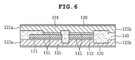
- FIGS. 5 and 6 each are cross-sectional views taken along the line A 1 -A 1 ′ and the line B 1 -B 1 ′ of FIG. 3 ;
- FIG. 7 is a plan view of a power module package including the unit power module according to the preferred embodiment of the present invention.
- FIGS. 8 and 9 each are cross-sectional views taken along the line A 2 -A 2 ′ and the line B 2 -B 2 ′ of FIG. 7 ;
- FIG. 10 is a plan view of a power module package including a unit power module according to another preferred embodiment of the present invention.
- FIGS. 11 and 12 each are cross-sectional views taken along the line A 3 -A 3 ′ and the line B 3 -B 3 ′ of FIG. 10 .
- FIG. 1 is a perspective view illustrating a structure of a unit power module according to a preferred embodiment of the present invention
- FIGS. 2A and 2B are plan views illustrating top and bottom surfaces of the unit power module according to the preferred embodiment of the present invention
- FIGS. 3 and 4 each illustrate one side view and the other side view of the unit power module according to the preferred embodiment of the present invention
- FIGS. 5 and 6 each are cross-sectional views taken along the line A 1 -A 1 ′ and the line B 1 -B 1 ′ of FIG. 3 .
- a unit power module 110 includes a first semiconductor chip 111 , a second semiconductor chip 113 , a first metal plate 121 , a second metal plate 123 , a third metal plate 125 , and a sealing member 140 .
- the first semiconductor chip 111 and the second semiconductor chip 113 may be power devices but, the preferred embodiment of the present invention is not particularly limited thereto.
- the power device may include a silicon controlled rectifier (SCR), a power transistor, an insulated gate bipolar transistor (IGBT), a MOS transistor, a power rectifier, a power regulator, an inverter, a converter, a high power semiconductor chip that is a combination thereof, a diode, and the like, but is not limited thereto.
- SCR silicon controlled rectifier
- IGBT insulated gate bipolar transistor
- MOS transistor MOS transistor
- a power rectifier a power regulator
- inverter a converter
- a high power semiconductor chip that is a combination thereof, a diode, and the like, but is not limited thereto.
- the insulated gate bipolar transistor is used as the first semiconductor chip 111 and the diode is used as the second semiconductor chip 113 , but this is only one embodiment.
- the present invention is not limited thereto, but other power devices can also be used.
- the insulated gate bipolar transistor (IGBT) is used as the first semiconductor chip 111 and the diode is used as the second semiconductor chip 113 will be described by way of example.
- the first semiconductor chip 111 has one surface and the other surface and the one surface may be provided with a 1-1-th electrode (not illustrated) and a 1-2-electrode (not illustrated) spaced apart from the 1-1-th electrode (not illustrated) and the other surface may be provided with a 1-3-th electrode (not illustrated).
- the second semiconductor chip 113 also has one surface and the other surface and the one surface may be provided with a 2-1-th electrode (not illustrated) and the other surface may be provided with a 2-2-th electrode (not illustrated).
- the 1-1-th electrode, the 1-2-th electrode, and the 1-3-th electrode of the first semiconductor chip 111 each are an emitter electrode, a gate electrode, and a collector electrode and the 2-1-th electrode and a 2-2-th electrode of the second semiconductor chip 113 each are an anode electrode and a cathode electrode.
- the emitter electrode of the first semiconductor chip 111 and the anode electrode of the second semiconductor chip 113 and the collector electrode of the first semiconductor chip 111 and the cathode electrode of the second semiconductor chip 113 may each be connected with a terminal having the same polarity.
- the emitter electrode of the first semiconductor chip 111 and the anode electrode of the second semiconductor chip 113 and the collector electrode of the first semiconductor chip 111 and the cathode electrode of the second semiconductor chip 113 may each be connected with one pattern.
- the first metal plate 121 , the second metal plate 123 , and the third plate 125 may be formed of copper (Cu), but the preferred embodiment of the present invention is not particularly limited thereto.
- the first metal plate 121 may be disposed to contact the emitter electrode of the first semiconductor chip 111 and the anode electrode of the second semiconductor chip 113
- the second metal plate 123 may be disposed to contact the gate electrode of the first semiconductor chip 111
- the third metal plate 125 may be disposed to contact the collector electrode of the first semiconductor chip 111 and the cathode electrode of the second semiconductor chip 113 .
- one surface of the first semiconductor chip 111 and the second semiconductor chip 113 is provided with the first metal plate 121 and the other surface thereof is provided with the third metal plate 125 to dispose the first semiconductor chip 111 and the second semiconductor chip 113 between the first metal plate 121 and the third metal plate 125 .
- one surface of the first semiconductor chip 111 is provided with the second metal plate 123 so as to be spaced apart from the first metal plate 121 .
- the unit power module 100 may further include a bonding member 115 that bonds the first metal plate 121 , the second metal plate 123 , and the third metal plate 125 to the first semiconductor chip 111 and the second semiconductor chip 113 .
- the bonding member 115 may be a solder, but the preferred embodiment of the present invention is not particularly limited thereto. Therefore, any conductive bonding material can be used.
- the sealing member 140 may be formed to surround the first metal plate 121 , the second metal plate 123 , and the third metal plate 125 , as illustrated in FIG. 1 .
- the first semiconductor chip 111 and the second semiconductor chip 113 that are disposed between the first metal plate 121 and the third metal plate 125 may also be sealed.
- sealing member 140 epoxy molded compound (EMC), and the like, may be used, but the preferred embodiment of the present invention is not particularly limited thereto.
- EMC epoxy molded compound
- the unit power module 100 may further include an insulating layer 130 formed on the first metal plate 121 and the third metal plate 125 , but the preferred embodiment of the present invention is not particularly limited thereto.
- the insulating layer 130 may be formed of the same material as the foregoing sealing member 140 , but the preferred embodiment of the present invention is not particularly limited thereto. Therefore, all materials used as an insulating material known in the art can be used.
- FIG. 1 illustrates that a thickness of the second metal plate 123 is smaller than that of the first metal plate 121 , which is only one preferred embodiment. Therefore, the thickness of the second metal plate may be formed to be the same as that of the first metal plate. If the second metal plate and the first metal plate are formed to have the same thickness, the insulating layer 130 may also be formed on the second metal plate 132 .
- the unit power module 100 has one side and the other side in a perpendicular direction to their thickness. Meanwhile, as illustrated in FIG. 3 , the first metal plate 121 , the second metal plate 123 , and the third metal plate 125 are exposed to the one side and as illustrated in FIG. 4 , the first metal plate 121 and the third metal plate 125 may be exposed to the other side.
- the first metal plate 121 , the second metal plate 123 , and the third metal plate 125 exposed to both sides are each named emitter pads 121 a and 121 b , a gate pad 123 a , and collector pads 125 a and 125 b.
- connection member 240 formed in an insertion groove 211 of a case 210 to be described below to electrically connect the first semiconductor chip 111 and the second semiconductor chip 113 within the unit power module 100 with the external connection terminal. This will be described below in detail.
- the first metal plate 121 , the second metal plate 123 , and the third metal plate 125 that are exposed to both sides of the unit power module 100 may be formed to have the same plane as the sealing member 140 and may be formed to be protruded from the sealing member 140 , but the preferred embodiment of the present invention is not particularly limited thereto.
- the power device equipped in the power module package can be manufactured in the module form to test the defect of the module manufactured before being packaged and then packages only the good product, such that the power module package can be manufactured, thereby reducing the failure cost.
- the metal plate corresponding to the circuit patterns according to the prior art can be bonded to all the electrodes of the semiconductor chip, respectively and then modularized to remove the use of the wire as compared with the case in which the circuit patterns according to the related art are electrically connected with the semiconductor using the wire, thereby simplifying the structure and the process and shortening the process time.
- FIG. 7 is a plan view of a power module package including the unit power module according to the preferred embodiment of the present invention
- FIGS. 8 and 9 each are cross-sectional views taken along the line A 2 -A 2 ′ and the line B 2 -B 2 ′ of FIG. 7
- FIG. 10 is a plan view of a power module package including a unit power module according to another preferred embodiment of the present invention
- FIGS. 11 and 12 each are cross-sectional views taken along the line A 3 -A 3 ′ and the line B 3 -B 3 ′ of FIG. 10 .
- a power module package 200 may include the unit power module 100 and the case 210 in which at least one unit power module 100 is received.
- unit power module 100 is described in detail with reference to the unit power module portion and therefore, will be briefly described herein.
- the unit power module 100 includes the first semiconductor chip 111 having the emitter electrode (not illustrated) and the gate electrode (not illustrated) spaced apart from the emitter electrode formed one surface thereof and the collector electrode (not illustrated) formed on the other side thereof, the second semiconductor chip 113 having the anode electrode (not illustrated) formed on one surface thereof and the cathode electrode (not illustrated) formed on the other surface thereof, the first metal plate 121 contacting the emitter electrode (not illustrated) of the first semiconductor chip 111 and the anode electrode of the second semiconductor chip 113 , the second metal plate 123 contacting the gate electrode (not illustrated) of the first semiconductor chip 111 , the third metal plate 125 contacting the collector electrode (not illustrated) of the first semiconductor chip 111 and the cathode electrode (not illustrated) of the second semiconductor chip 113 , and the sealing member 140 formed to surround the surfaces of the first metal plate 121 , the second metal plate 123 , and the third metal plate 125 .
- the surface of the first metal plate 121 and the surface of the third metal plate 125 may be further provided with the insulating layer 130 .
- the first metal plate 121 , the second metal plate 123 , and the third metal plate 125 may be exposed to one of both sides of the unit power module 100 and as illustrated in FIG. 4 , the first metal plate 121 and the third metal plate 125 may be exposed to the other side thereof.
- the first metal plate 121 , the second metal plate 123 , and the third metal plate 125 exposed to both sides are each named the emitter pads 121 a and 121 b , the gate pad 123 a , and the collector pads 125 a and 125 b.
- the case 210 may include the insertion groove 211 in which at least one unit power module 100 is received.
- the insertion groove 211 may be formed to penetrate through the case 210 in a thickness direction, but the preferred embodiment of the present invention is not limited thereto.
- the external connection terminal formed to be exposed to the surface of the case 210 may be further provided.
- the external connection terminal may include a power supply terminal 221 , a ground terminal 223 , a control terminal 225 , and output terminals 227 a , 227 b , and 227 c as illustrated in FIG. 7 , but the preferred embodiment of the present invention is not limited thereto.
- the power supply terminal 221 is a terminal for supplying power to the first semiconductor chip 111 and the second semiconductor chip 113 within the unit power module 100
- the ground terminal 223 is a terminal for connecting and grounding current flowing out from the first semiconductor chip 111 and the second semiconductor chip 113 by reference potential
- the control terminal 225 is a terminal for transferring a driving signal for driving the first semiconductor chip 111 to the gate electrode
- the output terminals 227 a , 227 b , and 227 c are terminals for transferring current output from the first semiconductor chip 111 and the second semiconductor chip 113 to the external apparatus.
- the reason of providing the output terminals 227 a , 227 b , and 227 c in three is to connect with loads of each phase of an external apparatus having a 3 phase load such as a 3 phase motor, which is only the preferred embodiment of the present invention. Therefore, the present invention is not particularly limited thereto.
- an output terminal 227 a may be called a U-phase output terminal 227 a and an output terminal 227 b may be called a V-phase output terminal 227 b , and an output terminal 227 c may be called a W-phase output terminal 227 c.
- the set module means two unit power modules 100 .
- a total of 6 unit power modules 100 that is, three sets of modules are received in the case 210 and the adjacent unit power modules 100 from the unit power module 100 outermost located among the unit power modules 100 received in a row are operated as one set.
- the case 210 is formed in the case 210 and has one end and the other end and the one end contacts the external connection terminal and the other end may further include circuit patterns 230 a , 230 b , 230 c , 230 d , 230 e , and 230 f formed toward the inside of the insertion groove 211 .
- the circuit pattern 230 a has one end contacting the power terminal 221
- the circuit pattern 230 b contacts one end contacting the ground terminal 223
- the circuit pattern 230 c has one end contacting the control terminal 225
- the circuit patterns 230 d , 230 e , and 230 f may each have ends that may be connected with the U-phase output terminal 227 a , the V-phase output terminal 227 b , and the W-phase output terminal 227 c.
- circuit pattern 230 a contacting the power supply terminal 221 and the circuit pattern 230 b contacting the ground terminal 223 are each connected with two unit power modules 100 included in the foregoing set module.
- the third metal plate 125 of one of the two adjacent unit power modules 100 is connected with the circuit pattern 230 a contacting the power supply terminal 221 and the first metal plate 121 of another unit power module 100 is connected with the circuit pattern 230 b contacting the ground terminal 223 .
- the other ends of the circuit patterns 230 d , 230 e , and 230 f of which the ends are each connected with the U-phase output terminal 227 a , the V-phase output terminal 227 b , and the W-phase output terminal 227 c , respectively, are divided into two branches as illustrated in FIG. 7 , such that one of the other ends of the circuit patterns 230 d , 230 e , and 230 f is connected with the first metal plate 121 of one unit power module 100 among the foregoing set modules and the other one of the other ends thereof may be connected with the third metal plate 125 of the other unit power module 100 .
- the output current is transferred to the output terminals 227 a , 227 b , and 227 c and is output to the outside and at the same time, is transferred to the other adjacent unit power modules 100 and flows in the ground terminal 223 and thus may be grounded.
- the case 210 has one end and the other end and the one end contacts the circuit patterns 230 a , 203 b , 230 c , 230 d , 230 e , and 230 f and the other end may further include the plurality of connection members 240 that are protruded to the inside of the insertion groove 211 to contact the emitter pads 121 and 121 b , the gate pad 123 a , and the collector pads 125 a and 125 b of the unit power module 100 , respectively.
- connection member 240 may be formed of materials having conductivity and elastic force.
- a spring formed of metal, and the like may be used, but the preferred embodiment of the present invention is not particularly limited thereto.
- the unit power module 100 may be easily detached/attached to/from the insertion groove 211 of the case 210 , similar to the method of attaching and detaching, for example, a battery.
- the unit power module 100 received in the insertion groove 211 of the case 210 is not fixed by a separate adhesive but can be detached/attached by the connection member 240 having elastic force, such that the unit power module 100 having a defect after being received can be replaced with the unit power module 100 that is a good product, thereby easily repairing the defective products.
- the external connection terminal including the power supply terminal 221 , the ground terminal 223 , the control terminal 225 , and the output terminals 227 a , 227 b , and 227 c , the circuit patterns 230 a , 230 b , 230 c , 230 d , 230 e , and 230 f connected with the external connection terminals, and the connection member 240 connected with the circuit patterns 230 a , 230 b , 230 c , 230 d , 230 e , and 230 f are formed.
- the unit power module 100 may perform the same function as the power module package in which the semiconductor chip is mounted on the substrate according to the related art and the external connection terminal is wire-bonded with the semiconductor chip and then is covered with the case.
- the driving signal is input through the control terminal 225 of the unit power module 100 a from the outside, the signal is transferred to the gate electrode through the circuit pattern 230 c , the connection member 240 , and the gate pad 123 a to drive the first semiconductor chip 111 .
- the current collected in the third metal plate 125 flows in the first metal plate 121 through the first semiconductor chip 111 and the second semiconductor chip 113 and the current flowing in the first metal plate 121 is output to the external apparatus through the emitter pad 121 b , the connection member 240 , the circuit pattern 230 d , and the U-phase output terminal 227 a.
- the driving signal is input through the control terminal 225 of the unit power module 100 b from the outside, the signal is transferred to the gate electrode through the circuit pattern 230 c , the connection member 240 , and the gate pad 123 a to drive the first semiconductor chip 111 .
- the current collected in the third metal plate 125 flows in the first metal plate 121 through the first semiconductor chip 111 and the second semiconductor chip 113 and the current flowing in the first metal plate 121 is output to the ground terminal 223 through the emitter pad 121 a , the connection member 240 , and the circuit pattern 230 b.
- a gap may be formed between the inner wall of the insertion groove 211 of the case 210 and the received unit power module 100 as illustrated in FIG. 7 . This is due to the connection member 240 formed to be protruded to the inside of the insertion groove 211 and the formed gap is filled with an insulating material to improve electrical reliability.
- the power module package 100 may be provided with a heat sink 300 contacting a top portion or a bottom portion of the case 210 .
- FIG. 8 illustrates that the heat sink 300 contacts the bottom portion of the case 210 , but the preferred embodiment of the present invention is not particularly limited thereto. Therefore, the heat sink may contact the top portion of the case 210 and may contact both of the top and bottom portions thereof.
- the heat sink 300 is to diffuse heat generated from the first semiconductor chip 111 and the second semiconductor chip 113 in the air, but the preferred embodiment of the present invention is not particularly limited thereto. Therefore, the heat sink 300 may be formed of materials such as copper (Cu) or tin (Sn).
- FIGS. 10 to 12 illustrate a structure of a power module package 400 according to a preferred embodiment of the present invention in which the unit power module 100 is not received in the power module package 200 of FIG. 7 in a single layer but is received so as to be laminated therein.
- the two unit power modules 100 that are a set module are laminated in two layers and received.
- the package size may be reduced half, as compared with the power module package 200 according to the foregoing preferred embodiment of the present invention.
- the operation of the power module package 400 is the same as the power module package 200 according to the foregoing preferred embodiment of the present invention and therefore, the detailed description thereof will be omitted.
- the power device equipped in the power module package can be manufactured in the unit module to test the non-defect/defect of the unit module manufactured before being packaged and then packages only the good product, such that the power module package can be manufactured, thereby reducing the failure cost.
- the metal plate corresponding to the circuit patterns according to the prior art can be bonded to all the electrodes of the semiconductor chip, respectively and then modularized to remove the wire bonding process as compared with the case in which the circuit patterns according to the related art are electrically connected with the semiconductor chip using the wire, thereby simplifying the process and shortening the process time.
- connection member having elastic force is protruded to the inner wall of the insertion groove of the case in which the unit power module is received to implement the detachment and attachment of the unit power module, such that only the defective unit power module can be replaced, thereby implementing the easy repairs at the time of the defect of products.
Abstract
Description
Claims (14)
Applications Claiming Priority (2)
| Application Number | Priority Date | Filing Date | Title |
|---|---|---|---|
| KR1020120121287A KR101482317B1 (en) | 2012-10-30 | 2012-10-30 | Unit power module and power module package comprising the same |
| KR10-2012-0121287 | 2012-10-30 |
Publications (2)
| Publication Number | Publication Date |
|---|---|
| US20140117408A1 US20140117408A1 (en) | 2014-05-01 |
| US9123683B2 true US9123683B2 (en) | 2015-09-01 |
Family
ID=50546218
Family Applications (1)
| Application Number | Title | Priority Date | Filing Date |
|---|---|---|---|
| US13/782,859 Expired - Fee Related US9123683B2 (en) | 2012-10-30 | 2013-03-01 | Unit power module and power module package comprising the same |
Country Status (2)
| Country | Link |
|---|---|
| US (1) | US9123683B2 (en) |
| KR (1) | KR101482317B1 (en) |
Families Citing this family (3)
| Publication number | Priority date | Publication date | Assignee | Title |
|---|---|---|---|---|
| JP5588895B2 (en) * | 2011-02-28 | 2014-09-10 | 日立オートモティブシステムズ株式会社 | Power semiconductor module, power semiconductor module manufacturing method, and power conversion device |
| KR102391008B1 (en) * | 2017-08-08 | 2022-04-26 | 현대자동차주식회사 | Power module and power conversion system including the power module |
| EP4010926A4 (en) * | 2020-11-02 | 2023-02-22 | Dynex Semiconductor Limited | High power density 3d semiconductor module packaging |
Citations (10)
| Publication number | Priority date | Publication date | Assignee | Title |
|---|---|---|---|---|
| JPH06232303A (en) | 1993-02-05 | 1994-08-19 | Fuji Electric Co Ltd | Power semiconductor device |
| US5901044A (en) * | 1997-07-10 | 1999-05-04 | Ilc Data Device Corporation | Mini-module with upwardly directed leads |
| US5920119A (en) | 1996-02-22 | 1999-07-06 | Hitachi, Ltd. | Power semiconductor module employing metal based molded case and screw fastening type terminals for high reliability |
| US6697257B1 (en) * | 1999-10-09 | 2004-02-24 | Robert Bosch Gmbh | Power semiconductor module |
| US20070132073A1 (en) * | 2005-12-09 | 2007-06-14 | Tiong Toong T | Device and method for assembling a top and bottom exposed packaged semiconductor |
| KR20080008218A (en) | 2006-07-18 | 2008-01-23 | 미쓰비시덴키 가부시키가이샤 | Power semiconductor apparatus |
| US20080192437A1 (en) * | 2005-03-23 | 2008-08-14 | Toyota Jidosha Kabushiki Kaisha | Power Semiconductor Module |
| JP2008270527A (en) | 2007-04-20 | 2008-11-06 | Mitsubishi Electric Corp | Power semiconductor module |
| US20110254177A1 (en) * | 2006-08-29 | 2011-10-20 | Denso Corporation | Power electronic package having two substrates with multiple semiconductor chips and electronic components |
| US20120211767A1 (en) * | 2009-08-03 | 2012-08-23 | Kabushiki Kaisha Yaskawa Denki | Power converter |
-
2012
- 2012-10-30 KR KR1020120121287A patent/KR101482317B1/en active IP Right Grant
-
2013
- 2013-03-01 US US13/782,859 patent/US9123683B2/en not_active Expired - Fee Related
Patent Citations (10)
| Publication number | Priority date | Publication date | Assignee | Title |
|---|---|---|---|---|
| JPH06232303A (en) | 1993-02-05 | 1994-08-19 | Fuji Electric Co Ltd | Power semiconductor device |
| US5920119A (en) | 1996-02-22 | 1999-07-06 | Hitachi, Ltd. | Power semiconductor module employing metal based molded case and screw fastening type terminals for high reliability |
| US5901044A (en) * | 1997-07-10 | 1999-05-04 | Ilc Data Device Corporation | Mini-module with upwardly directed leads |
| US6697257B1 (en) * | 1999-10-09 | 2004-02-24 | Robert Bosch Gmbh | Power semiconductor module |
| US20080192437A1 (en) * | 2005-03-23 | 2008-08-14 | Toyota Jidosha Kabushiki Kaisha | Power Semiconductor Module |
| US20070132073A1 (en) * | 2005-12-09 | 2007-06-14 | Tiong Toong T | Device and method for assembling a top and bottom exposed packaged semiconductor |
| KR20080008218A (en) | 2006-07-18 | 2008-01-23 | 미쓰비시덴키 가부시키가이샤 | Power semiconductor apparatus |
| US20110254177A1 (en) * | 2006-08-29 | 2011-10-20 | Denso Corporation | Power electronic package having two substrates with multiple semiconductor chips and electronic components |
| JP2008270527A (en) | 2007-04-20 | 2008-11-06 | Mitsubishi Electric Corp | Power semiconductor module |
| US20120211767A1 (en) * | 2009-08-03 | 2012-08-23 | Kabushiki Kaisha Yaskawa Denki | Power converter |
Non-Patent Citations (1)
| Title |
|---|
| Office action dated Oct. 15, 2013 from corresponding Korean Patent Application No. 10-2012-0121287 and its English summary provided by the clients. |
Also Published As
| Publication number | Publication date |
|---|---|
| KR20140055038A (en) | 2014-05-09 |
| KR101482317B1 (en) | 2015-01-13 |
| US20140117408A1 (en) | 2014-05-01 |
Similar Documents
| Publication | Publication Date | Title |
|---|---|---|
| US20160005675A1 (en) | Double sided cooling chip package and method of manufacturing the same | |
| US20140334203A1 (en) | Power converter and method for manufacturing power converter | |
| US20170110395A1 (en) | Semiconductor device | |
| US9013065B2 (en) | Connecting mechanism arrangeable to a photovoltaic module | |
| US9001518B2 (en) | Power module with press-fit clamps | |
| US9117688B2 (en) | Semiconductor device, inverter device provided with semiconductor device, and in-vehicle rotating electrical machine provided with semiconductor device and inverter device | |
| JP6408857B2 (en) | Gate driver unit and power module | |
| US10566316B2 (en) | Semiconductor device and power conversion apparatus | |
| US10192806B2 (en) | Semiconductor device | |
| US9123683B2 (en) | Unit power module and power module package comprising the same | |
| US10304777B2 (en) | Semiconductor device having a plurality of semiconductor modules connected by a connection component | |
| JP5081951B2 (en) | Inverter device | |
| CN112701094A (en) | Power device packaging structure and power electronic equipment | |
| JP5817702B2 (en) | Semiconductor module | |
| JP6156131B2 (en) | Semiconductor device | |
| US9209099B1 (en) | Power semiconductor module | |
| CN103296019A (en) | Semiconductor device and method for manufacturing semiconductor device | |
| WO2020035931A1 (en) | Semiconductor module | |
| JP2016076727A (en) | Semiconductor device | |
| KR20170068271A (en) | Power module | |
| JP5891744B2 (en) | Semiconductor device | |
| JP2018032835A (en) | Semiconductor device manufacturing method | |
| CN204558445U (en) | Semiconductor packaging structure | |
| US20230274990A1 (en) | Power Semiconductor Module System and Method for Producing the Power Semiconductor Module System | |
| JP2013098343A (en) | Semiconductor device and method of manufacturing the same |
Legal Events
| Date | Code | Title | Description |
|---|---|---|---|
| AS | Assignment |
Owner name: SAMSUNG ELECTRO-MECHANICS CO., LTD., KOREA, REPUBL Free format text: ASSIGNMENT OF ASSIGNORS INTEREST;ASSIGNORS:KIM, TAE HYUN;SUH, BUM SEOK;YOO, DO JAE;AND OTHERS;REEL/FRAME:029909/0043 Effective date: 20130123 |
|
| STCF | Information on status: patent grant |
Free format text: PATENTED CASE |
|
| FEPP | Fee payment procedure |
Free format text: PAYOR NUMBER ASSIGNED (ORIGINAL EVENT CODE: ASPN); ENTITY STATUS OF PATENT OWNER: LARGE ENTITY |
|
| MAFP | Maintenance fee payment |
Free format text: PAYMENT OF MAINTENANCE FEE, 4TH YEAR, LARGE ENTITY (ORIGINAL EVENT CODE: M1551); ENTITY STATUS OF PATENT OWNER: LARGE ENTITY Year of fee payment: 4 |
|
| FEPP | Fee payment procedure |
Free format text: MAINTENANCE FEE REMINDER MAILED (ORIGINAL EVENT CODE: REM.); ENTITY STATUS OF PATENT OWNER: LARGE ENTITY |
|
| LAPS | Lapse for failure to pay maintenance fees |
Free format text: PATENT EXPIRED FOR FAILURE TO PAY MAINTENANCE FEES (ORIGINAL EVENT CODE: EXP.); ENTITY STATUS OF PATENT OWNER: LARGE ENTITY |
|
| STCH | Information on status: patent discontinuation |
Free format text: PATENT EXPIRED DUE TO NONPAYMENT OF MAINTENANCE FEES UNDER 37 CFR 1.362 |
|
| FP | Lapsed due to failure to pay maintenance fee |
Effective date: 20230901 |