US9099378B2 - Schottky barrier diode and method of manufacturing the same - Google Patents
Schottky barrier diode and method of manufacturing the same Download PDFInfo
- Publication number
- US9099378B2 US9099378B2 US13/710,119 US201213710119A US9099378B2 US 9099378 B2 US9099378 B2 US 9099378B2 US 201213710119 A US201213710119 A US 201213710119A US 9099378 B2 US9099378 B2 US 9099378B2
- Authority
- US
- United States
- Prior art keywords
- region
- epitaxial layer
- type epitaxial
- disposed
- barrier diode
- Prior art date
- Legal status (The legal status is an assumption and is not a legal conclusion. Google has not performed a legal analysis and makes no representation as to the accuracy of the status listed.)
- Active
Links
- 230000004888 barrier function Effects 0.000 title claims abstract description 17
- 238000004519 manufacturing process Methods 0.000 title description 6
- 239000000758 substrate Substances 0.000 claims abstract description 15
- HBMJWWWQQXIZIP-UHFFFAOYSA-N silicon carbide Chemical compound [Si+]#[C-] HBMJWWWQQXIZIP-UHFFFAOYSA-N 0.000 claims abstract description 14
- 229910010271 silicon carbide Inorganic materials 0.000 claims abstract description 13
- 150000002500 ions Chemical class 0.000 description 6
- 238000012986 modification Methods 0.000 description 3
- 230000004048 modification Effects 0.000 description 3
- 238000000034 method Methods 0.000 description 2
- 239000004065 semiconductor Substances 0.000 description 2
- 230000000903 blocking effect Effects 0.000 description 1
- 230000015556 catabolic process Effects 0.000 description 1
- 239000000470 constituent Substances 0.000 description 1
- 239000002184 metal Substances 0.000 description 1
- 230000008569 process Effects 0.000 description 1
- 230000009467 reduction Effects 0.000 description 1
Images


Classifications
-
- H—ELECTRICITY
- H01—ELECTRIC ELEMENTS
- H01L—SEMICONDUCTOR DEVICES NOT COVERED BY CLASS H10
- H01L21/00—Processes or apparatus adapted for the manufacture or treatment of semiconductor or solid state devices or of parts thereof
- H01L21/02—Manufacture or treatment of semiconductor devices or of parts thereof
- H01L21/04—Manufacture or treatment of semiconductor devices or of parts thereof the devices having at least one potential-jump barrier or surface barrier, e.g. PN junction, depletion layer or carrier concentration layer
- H01L21/18—Manufacture or treatment of semiconductor devices or of parts thereof the devices having at least one potential-jump barrier or surface barrier, e.g. PN junction, depletion layer or carrier concentration layer the devices having semiconductor bodies comprising elements of Group IV of the Periodic System or AIIIBV compounds with or without impurities, e.g. doping materials
-
- H—ELECTRICITY
- H01—ELECTRIC ELEMENTS
- H01L—SEMICONDUCTOR DEVICES NOT COVERED BY CLASS H10
- H01L29/00—Semiconductor devices adapted for rectifying, amplifying, oscillating or switching, or capacitors or resistors with at least one potential-jump barrier or surface barrier, e.g. PN junction depletion layer or carrier concentration layer; Details of semiconductor bodies or of electrodes thereof ; Multistep manufacturing processes therefor
- H01L29/02—Semiconductor bodies ; Multistep manufacturing processes therefor
- H01L29/12—Semiconductor bodies ; Multistep manufacturing processes therefor characterised by the materials of which they are formed
- H01L29/16—Semiconductor bodies ; Multistep manufacturing processes therefor characterised by the materials of which they are formed including, apart from doping materials or other impurities, only elements of Group IV of the Periodic System
- H01L29/1608—Silicon carbide
-
- H—ELECTRICITY
- H01—ELECTRIC ELEMENTS
- H01L—SEMICONDUCTOR DEVICES NOT COVERED BY CLASS H10
- H01L29/00—Semiconductor devices adapted for rectifying, amplifying, oscillating or switching, or capacitors or resistors with at least one potential-jump barrier or surface barrier, e.g. PN junction depletion layer or carrier concentration layer; Details of semiconductor bodies or of electrodes thereof ; Multistep manufacturing processes therefor
- H01L29/02—Semiconductor bodies ; Multistep manufacturing processes therefor
- H01L29/06—Semiconductor bodies ; Multistep manufacturing processes therefor characterised by their shape; characterised by the shapes, relative sizes, or dispositions of the semiconductor regions ; characterised by the concentration or distribution of impurities within semiconductor regions
- H01L29/0603—Semiconductor bodies ; Multistep manufacturing processes therefor characterised by their shape; characterised by the shapes, relative sizes, or dispositions of the semiconductor regions ; characterised by the concentration or distribution of impurities within semiconductor regions characterised by particular constructional design considerations, e.g. for preventing surface leakage, for controlling electric field concentration or for internal isolations regions
- H01L29/0607—Semiconductor bodies ; Multistep manufacturing processes therefor characterised by their shape; characterised by the shapes, relative sizes, or dispositions of the semiconductor regions ; characterised by the concentration or distribution of impurities within semiconductor regions characterised by particular constructional design considerations, e.g. for preventing surface leakage, for controlling electric field concentration or for internal isolations regions for preventing surface leakage or controlling electric field concentration
- H01L29/0611—Semiconductor bodies ; Multistep manufacturing processes therefor characterised by their shape; characterised by the shapes, relative sizes, or dispositions of the semiconductor regions ; characterised by the concentration or distribution of impurities within semiconductor regions characterised by particular constructional design considerations, e.g. for preventing surface leakage, for controlling electric field concentration or for internal isolations regions for preventing surface leakage or controlling electric field concentration for increasing or controlling the breakdown voltage of reverse biased devices
- H01L29/0615—Semiconductor bodies ; Multistep manufacturing processes therefor characterised by their shape; characterised by the shapes, relative sizes, or dispositions of the semiconductor regions ; characterised by the concentration or distribution of impurities within semiconductor regions characterised by particular constructional design considerations, e.g. for preventing surface leakage, for controlling electric field concentration or for internal isolations regions for preventing surface leakage or controlling electric field concentration for increasing or controlling the breakdown voltage of reverse biased devices by the doping profile or the shape or the arrangement of the PN junction, or with supplementary regions, e.g. junction termination extension [JTE]
- H01L29/0619—Semiconductor bodies ; Multistep manufacturing processes therefor characterised by their shape; characterised by the shapes, relative sizes, or dispositions of the semiconductor regions ; characterised by the concentration or distribution of impurities within semiconductor regions characterised by particular constructional design considerations, e.g. for preventing surface leakage, for controlling electric field concentration or for internal isolations regions for preventing surface leakage or controlling electric field concentration for increasing or controlling the breakdown voltage of reverse biased devices by the doping profile or the shape or the arrangement of the PN junction, or with supplementary regions, e.g. junction termination extension [JTE] with a supplementary region doped oppositely to or in rectifying contact with the semiconductor containing or contacting region, e.g. guard rings with PN or Schottky junction
- H01L29/0623—Buried supplementary region, e.g. buried guard ring
-
- H—ELECTRICITY
- H01—ELECTRIC ELEMENTS
- H01L—SEMICONDUCTOR DEVICES NOT COVERED BY CLASS H10
- H01L29/00—Semiconductor devices adapted for rectifying, amplifying, oscillating or switching, or capacitors or resistors with at least one potential-jump barrier or surface barrier, e.g. PN junction depletion layer or carrier concentration layer; Details of semiconductor bodies or of electrodes thereof ; Multistep manufacturing processes therefor
- H01L29/66—Types of semiconductor device ; Multistep manufacturing processes therefor
- H01L29/66007—Multistep manufacturing processes
- H01L29/66053—Multistep manufacturing processes of devices having a semiconductor body comprising crystalline silicon carbide
- H01L29/6606—Multistep manufacturing processes of devices having a semiconductor body comprising crystalline silicon carbide the devices being controllable only by variation of the electric current supplied or the electric potential applied, to one or more of the electrodes carrying the current to be rectified, amplified, oscillated or switched, e.g. two-terminal devices
-
- H—ELECTRICITY
- H01—ELECTRIC ELEMENTS
- H01L—SEMICONDUCTOR DEVICES NOT COVERED BY CLASS H10
- H01L29/00—Semiconductor devices adapted for rectifying, amplifying, oscillating or switching, or capacitors or resistors with at least one potential-jump barrier or surface barrier, e.g. PN junction depletion layer or carrier concentration layer; Details of semiconductor bodies or of electrodes thereof ; Multistep manufacturing processes therefor
- H01L29/66—Types of semiconductor device ; Multistep manufacturing processes therefor
- H01L29/66007—Multistep manufacturing processes
- H01L29/66053—Multistep manufacturing processes of devices having a semiconductor body comprising crystalline silicon carbide
- H01L29/66068—Multistep manufacturing processes of devices having a semiconductor body comprising crystalline silicon carbide the devices being controllable only by the electric current supplied or the electric potential applied, to an electrode which does not carry the current to be rectified, amplified or switched, e.g. three-terminal devices
-
- H—ELECTRICITY
- H01—ELECTRIC ELEMENTS
- H01L—SEMICONDUCTOR DEVICES NOT COVERED BY CLASS H10
- H01L29/00—Semiconductor devices adapted for rectifying, amplifying, oscillating or switching, or capacitors or resistors with at least one potential-jump barrier or surface barrier, e.g. PN junction depletion layer or carrier concentration layer; Details of semiconductor bodies or of electrodes thereof ; Multistep manufacturing processes therefor
- H01L29/66—Types of semiconductor device ; Multistep manufacturing processes therefor
- H01L29/86—Types of semiconductor device ; Multistep manufacturing processes therefor controllable only by variation of the electric current supplied, or only the electric potential applied, to one or more of the electrodes carrying the current to be rectified, amplified, oscillated or switched
- H01L29/861—Diodes
- H01L29/872—Schottky diodes
Definitions
- the present invention relates to a schottky barrier diode including silicon carbide (SiC), and a method of manufacturing the same.
- a schottky barrier diode uses a schottky junction which is a junction of metal and a semiconductor without using PN junction unlike a general PN diode, exhibits a rapid switching characteristic, and has a turn-on voltage characteristic that is lower than that of the PN diode.
- JBS junction barrier schottky
- the p+ region exists in the schottky junction portion, there is a problem in that a contact area of a schottky electrode and an n ⁇ drift layer, which serves to be a current path in a forward direction, is reduced to increase a resistance value, and on-resistance of the schottky barrier diode is increased. Further, since the p+ region floats, a width of the depletion layer blocking the leak current is not large, and thus there is a difficulty during a process in that an interval between the p+ regions is reduced.
- Various aspects of the present invention are directed to maximize a schottky junction area to reduce on-resistance when a forward direction voltage is applied in a schottky barrier diode.
- a schottky barrier diode may include an n ⁇ type epitaxial layer disposed on a first surface of an n+ type silicon carbide substrate, a first p+ region disposed in the n ⁇ type epitaxial layer, an n type epitaxial layer disposed on the n ⁇ type epitaxial layer and the first p+ region, a second p+ region disposed in the n type epitaxial layer, a schottky electrode disposed on the n type epitaxial layer and the second p+ region, and an ohmic electrode disposed on a second surface of the n+ type silicon carbide substrate, wherein the first p+ region and the second p+ region are in contact with each other.
- the second p+ region may be formed in a quadrangle shape surrounding an edge of the n type epitaxial layer.
- a method of manufacturing a schottky barrier diode may include forming an n ⁇ type epitaxial layer on a first surface of an n+ type silicon carbide substrate, injecting p+ ions into a surface of the n ⁇ type epitaxial layer to form a first p+ region, forming an n type epitaxial layer on the n ⁇ type epitaxial layer and the first p+ region, injecting n+ ions into a surface of the n type epitaxial layer to form a second p+ region, forming a schottky electrode on the n type epitaxial layer and the second p+ region, and forming an ohmic electrode on a second surface of the n+ type silicon carbide substrate, wherein the first p+region and the second p+ region are in contact with each other.
- the first p+ region may be formed in a lattice shape on the surface of the n ⁇ type epitaxial layer.
- FIG. 1 is a cross-sectional view of a schottky barrier diode according to an exemplary embodiment of the present invention.
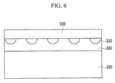
- FIG. 2 is a top plan view of an n ⁇ type epitaxial layer of FIG. 1 .
- an n ⁇ type epitaxial layer 200 , an n type epitaxial layer 300 , and a schottky electrode 400 are sequentially laminated on a first surface of an n+ type silicon carbide substrate 100 , and an ohmic electrode 500 is laminated on a second surface of the n+ type silicon carbide substrate 100 .
- a first p+ region 210 into which p+ ions are injected is formed in the n ⁇ type epitaxial layer 200
- a second p+ region 310 into which the p+ ions are injected is formed in the n type epitaxial layer 300 .
- the first p+ region 210 is formed in a lattice shape on a surface of the n ⁇ type epitaxial layer 200 .
- the second p+ region 310 is formed in a quadrangle shape surrounding an edge of the n type epitaxial layer 300 , and is in contact with the first p+ region 210 .
- first p+ region 210 and the second p+ region 310 are in contact with each other to be electrically connected, a reverse bias is applied to a junction region of the first p+ region 210 and the n ⁇ type epitaxial layer 200 when the reverse bias is applied, and thus a depletion layer that is wider than a known matter is formed to largely reduce a leak current.
- first p+ region 210 may be formed on the surface of the n ⁇ type epitaxial layer 200
- second p+ region 310 that is in contact with the first p+ region 210 may be formed at an edge of the n type epitaxial layer 300 to increase a schottky junction area, thus reducing on-resistance when the forward direction voltage is applied.
- FIGS. 4 to 7 and FIG. 1 a method of manufacturing the semiconductor device according to the exemplary embodiment of the present invention will be described in detail.
- FIGS. 4 to 7 are views sequentially illustrating a method of manufacturing the schottky barrier diode according to the exemplary embodiment of the present invention.
- the first p+ region 210 is formed by injecting p+ ions into a portion of the surface of the n ⁇ type epitaxial layer 200 .
- the first p+ region 210 is formed in a lattice shape on the surface of the n ⁇ type epitaxial layer 200 .
- the second p+ region 310 is formed by injecting p+ ions into a portion of the surface of the n type epitaxial layer 300 .
- the second p+ region 310 is formed in a quadrangle shape surrounding the edge of the n type epitaxial layer 300 .
- the second p+region 310 is in contact with the first p+ region 210 .
- a schottky electrode 400 is formed on the n type epitaxial layer 300 and the second p+ region 310 , and an ohmic electrode 500 is formed on the second surface of the n+ type silicon carbide substrate 100 .
Abstract
Description
Claims (2)
Applications Claiming Priority (2)
| Application Number | Priority Date | Filing Date | Title |
|---|---|---|---|
| KR1020120101967A KR101416361B1 (en) | 2012-09-14 | 2012-09-14 | Shottky barrier diode and method for manufacturing the same |
| KR10-2012-0101967 | 2012-09-14 |
Publications (2)
| Publication Number | Publication Date |
|---|---|
| US20140077225A1 US20140077225A1 (en) | 2014-03-20 |
| US9099378B2 true US9099378B2 (en) | 2015-08-04 |
Family
ID=50181574
Family Applications (1)
| Application Number | Title | Priority Date | Filing Date |
|---|---|---|---|
| US13/710,119 Active US9099378B2 (en) | 2012-09-14 | 2012-12-10 | Schottky barrier diode and method of manufacturing the same |
Country Status (5)
| Country | Link |
|---|---|
| US (1) | US9099378B2 (en) |
| JP (1) | JP2014060376A (en) |
| KR (1) | KR101416361B1 (en) |
| CN (1) | CN103681883A (en) |
| DE (1) | DE102012113027A1 (en) |
Families Citing this family (8)
| Publication number | Priority date | Publication date | Assignee | Title |
|---|---|---|---|---|
| KR20140085141A (en) * | 2012-12-27 | 2014-07-07 | 현대자동차주식회사 | Semiconductor device and method manufacturing the same |
| KR101360070B1 (en) * | 2012-12-27 | 2014-02-12 | 현대자동차 주식회사 | Semiconductor device and method manufacturing the same |
| KR101518905B1 (en) | 2013-12-30 | 2015-05-11 | 현대자동차 주식회사 | Shottky barrier diode and method for manufacturing the same |
| CN104576762B (en) * | 2014-12-25 | 2018-08-28 | 株洲南车时代电气股份有限公司 | Schottky-barrier diode and its manufacturing method |
| JP7098906B2 (en) * | 2017-10-11 | 2022-07-12 | 株式会社デンソー | Silicon carbide semiconductor device equipped with Schottky barrier diode and its manufacturing method |
| CN113937168A (en) * | 2020-07-13 | 2022-01-14 | 珠海格力电器股份有限公司 | Silicon carbide junction barrier schottky semiconductor device and method for manufacturing same |
| CN112687750B (en) * | 2020-12-10 | 2022-03-18 | 复旦大学 | SiC SBD device with semi-floating structure and preparation method thereof |
| CN113130625B (en) * | 2021-03-26 | 2021-11-12 | 先之科半导体科技(东莞)有限公司 | High-voltage rapid silicon carbide diode and preparation method thereof |
Citations (8)
| Publication number | Priority date | Publication date | Assignee | Title |
|---|---|---|---|---|
| US4134123A (en) * | 1976-08-09 | 1979-01-09 | U.S. Philips Corporation | High voltage Schottky barrier diode |
| JPH06112216A (en) | 1992-09-25 | 1994-04-22 | Toshiba Corp | High breakdown strength semiconductor device |
| JP2002314099A (en) | 2001-04-09 | 2002-10-25 | Denso Corp | Schottky diode and its manufacturing method |
| JP2005229071A (en) | 2004-02-16 | 2005-08-25 | Matsushita Electric Ind Co Ltd | Schottky barrier diode |
| US20060255423A1 (en) * | 2005-05-11 | 2006-11-16 | Sei-Hyung Ryu | Silicon carbide junction barrier schottky diodes with supressed minority carrier injection |
| US20080258153A1 (en) | 2007-04-18 | 2008-10-23 | Denso Corporation | Silcon carbide semiconductor device having schottky barrier diode and method for manufacturing the same |
| US20080296587A1 (en) | 2007-05-30 | 2008-12-04 | Denso Corporation | Silicon carbide semiconductor device having junction barrier schottky diode |
| US20090160008A1 (en) * | 2007-12-25 | 2009-06-25 | Hirokazu Fujiwara | Semiconductor device and method of manufacturing the same |
Family Cites Families (3)
| Publication number | Priority date | Publication date | Assignee | Title |
|---|---|---|---|---|
| JP3737524B2 (en) * | 1994-02-10 | 2006-01-18 | 新電元工業株式会社 | Rectification semiconductor device |
| JPH11330498A (en) * | 1998-05-07 | 1999-11-30 | Fuji Electric Co Ltd | Schottky barrier diode and fabrication thereof |
| KR101374312B1 (en) | 2011-10-21 | 2014-03-14 | 주식회사 지2터치 | Capacitive type touch detecting means, method and touch screen panel using voltage changing phenomenon, and display device embedding said the capacitive type touch screen panel |
-
2012
- 2012-09-14 KR KR1020120101967A patent/KR101416361B1/en active IP Right Grant
- 2012-11-30 JP JP2012262830A patent/JP2014060376A/en active Pending
- 2012-12-10 US US13/710,119 patent/US9099378B2/en active Active
- 2012-12-21 DE DE102012113027.2A patent/DE102012113027A1/en not_active Ceased
- 2012-12-25 CN CN201210570518.XA patent/CN103681883A/en active Pending
Patent Citations (8)
| Publication number | Priority date | Publication date | Assignee | Title |
|---|---|---|---|---|
| US4134123A (en) * | 1976-08-09 | 1979-01-09 | U.S. Philips Corporation | High voltage Schottky barrier diode |
| JPH06112216A (en) | 1992-09-25 | 1994-04-22 | Toshiba Corp | High breakdown strength semiconductor device |
| JP2002314099A (en) | 2001-04-09 | 2002-10-25 | Denso Corp | Schottky diode and its manufacturing method |
| JP2005229071A (en) | 2004-02-16 | 2005-08-25 | Matsushita Electric Ind Co Ltd | Schottky barrier diode |
| US20060255423A1 (en) * | 2005-05-11 | 2006-11-16 | Sei-Hyung Ryu | Silicon carbide junction barrier schottky diodes with supressed minority carrier injection |
| US20080258153A1 (en) | 2007-04-18 | 2008-10-23 | Denso Corporation | Silcon carbide semiconductor device having schottky barrier diode and method for manufacturing the same |
| US20080296587A1 (en) | 2007-05-30 | 2008-12-04 | Denso Corporation | Silicon carbide semiconductor device having junction barrier schottky diode |
| US20090160008A1 (en) * | 2007-12-25 | 2009-06-25 | Hirokazu Fujiwara | Semiconductor device and method of manufacturing the same |
Also Published As
| Publication number | Publication date |
|---|---|
| CN103681883A (en) | 2014-03-26 |
| JP2014060376A (en) | 2014-04-03 |
| KR101416361B1 (en) | 2014-08-06 |
| KR20140035594A (en) | 2014-03-24 |
| US20140077225A1 (en) | 2014-03-20 |
| DE102012113027A1 (en) | 2014-03-20 |
Similar Documents
| Publication | Publication Date | Title |
|---|---|---|
| US9099378B2 (en) | Schottky barrier diode and method of manufacturing the same | |
| TWI596783B (en) | Semiconductor device | |
| US8809969B2 (en) | Semiconductor device | |
| JP4621708B2 (en) | Semiconductor device and manufacturing method thereof | |
| JP4314277B2 (en) | SiC Schottky barrier semiconductor device | |
| JP2019071313A (en) | Semiconductor device | |
| US8890169B2 (en) | Semiconductor device | |
| US7915705B2 (en) | SiC semiconductor device having outer periphery structure | |
| US9368649B2 (en) | Schottky barrier diode and method of manufacturing the same | |
| US10930797B2 (en) | Schottky barrier diode and method of manufacturing the same | |
| US9159847B2 (en) | Schottky barrier diode and method of manufacturing the same | |
| US9236500B2 (en) | Schottky barrier diode and method for manufacturing schottky barrier diode | |
| KR20130049919A (en) | Silicon carbide schottky-barrier diode and method for manufacturing thr same | |
| KR101490937B1 (en) | Schottky barrier diode and method for manufacturing the same | |
| TWI620251B (en) | Semiconductor device | |
| US10985241B2 (en) | Semiconductor device and production method thereof | |
| KR20140079027A (en) | Schottky barrier diode and method for manufacturing the same | |
| JP2007235064A (en) | Schottky barrier semiconductor device, and method of manufacturing same | |
| US9960247B2 (en) | Schottky barrier structure for silicon carbide (SiC) power devices | |
| KR20160116294A (en) | Schottky diode | |
| JP2005045212A (en) | Schottky barrier diode and manufacturing method thereof |
Legal Events
| Date | Code | Title | Description |
|---|---|---|---|
| AS | Assignment |
Owner name: HYUNDAI MOTOR COMPANY, KOREA, REPUBLIC OF Free format text: ASSIGNMENT OF ASSIGNORS INTEREST;ASSIGNORS:LEE, JONG SEOK;HONG, KYOUNG-KOOK;REEL/FRAME:029439/0893 Effective date: 20121207 |
|
| FEPP | Fee payment procedure |
Free format text: PAYOR NUMBER ASSIGNED (ORIGINAL EVENT CODE: ASPN); ENTITY STATUS OF PATENT OWNER: LARGE ENTITY |
|
| STCF | Information on status: patent grant |
Free format text: PATENTED CASE |
|
| MAFP | Maintenance fee payment |
Free format text: PAYMENT OF MAINTENANCE FEE, 4TH YEAR, LARGE ENTITY (ORIGINAL EVENT CODE: M1551); ENTITY STATUS OF PATENT OWNER: LARGE ENTITY Year of fee payment: 4 |
|
| MAFP | Maintenance fee payment |
Free format text: PAYMENT OF MAINTENANCE FEE, 8TH YEAR, LARGE ENTITY (ORIGINAL EVENT CODE: M1552); ENTITY STATUS OF PATENT OWNER: LARGE ENTITY Year of fee payment: 8 |