US9007541B2 - Pixel array and display panel - Google Patents
Pixel array and display panel Download PDFInfo
- Publication number
- US9007541B2 US9007541B2 US13/615,598 US201213615598A US9007541B2 US 9007541 B2 US9007541 B2 US 9007541B2 US 201213615598 A US201213615598 A US 201213615598A US 9007541 B2 US9007541 B2 US 9007541B2
- Authority
- US
- United States
- Prior art keywords
- thin
- electrode
- film transistor
- plane
- same
- Prior art date
- Legal status (The legal status is an assumption and is not a legal conclusion. Google has not performed a legal analysis and makes no representation as to the accuracy of the status listed.)
- Active, expires
Links
- 239000010409 thin film Substances 0.000 claims abstract description 151
- 239000004020 conductor Substances 0.000 claims description 40
- 239000003990 capacitor Substances 0.000 claims description 35
- 239000000758 substrate Substances 0.000 claims description 26
- 238000013461 design Methods 0.000 description 25
- 230000003071 parasitic effect Effects 0.000 description 9
- 238000010586 diagram Methods 0.000 description 6
- 239000004973 liquid crystal related substance Substances 0.000 description 5
- 238000004519 manufacturing process Methods 0.000 description 5
- 239000007769 metal material Substances 0.000 description 5
- 239000002184 metal Substances 0.000 description 4
- MWUXSHHQAYIFBG-UHFFFAOYSA-N Nitric oxide Chemical compound O=[N] MWUXSHHQAYIFBG-UHFFFAOYSA-N 0.000 description 3
- 238000000034 method Methods 0.000 description 3
- 241001270131 Agaricus moelleri Species 0.000 description 2
- 230000008901 benefit Effects 0.000 description 2
- 238000011161 development Methods 0.000 description 2
- 230000005684 electric field Effects 0.000 description 2
- 239000000463 material Substances 0.000 description 2
- 239000000956 alloy Substances 0.000 description 1
- 229910045601 alloy Inorganic materials 0.000 description 1
- 230000004075 alteration Effects 0.000 description 1
- 238000012986 modification Methods 0.000 description 1
- 230000004048 modification Effects 0.000 description 1
- 150000004767 nitrides Chemical class 0.000 description 1
- 238000012360 testing method Methods 0.000 description 1
Images


Classifications
-
- H—ELECTRICITY
- H01—ELECTRIC ELEMENTS
- H01L—SEMICONDUCTOR DEVICES NOT COVERED BY CLASS H10
- H01L27/00—Devices consisting of a plurality of semiconductor or other solid-state components formed in or on a common substrate
- H01L27/02—Devices consisting of a plurality of semiconductor or other solid-state components formed in or on a common substrate including semiconductor components specially adapted for rectifying, oscillating, amplifying or switching and having potential barriers; including integrated passive circuit elements having potential barriers
- H01L27/12—Devices consisting of a plurality of semiconductor or other solid-state components formed in or on a common substrate including semiconductor components specially adapted for rectifying, oscillating, amplifying or switching and having potential barriers; including integrated passive circuit elements having potential barriers the substrate being other than a semiconductor body, e.g. an insulating body
- H01L27/1214—Devices consisting of a plurality of semiconductor or other solid-state components formed in or on a common substrate including semiconductor components specially adapted for rectifying, oscillating, amplifying or switching and having potential barriers; including integrated passive circuit elements having potential barriers the substrate being other than a semiconductor body, e.g. an insulating body comprising a plurality of TFTs formed on a non-semiconducting substrate, e.g. driving circuits for AMLCDs
- H01L27/124—Devices consisting of a plurality of semiconductor or other solid-state components formed in or on a common substrate including semiconductor components specially adapted for rectifying, oscillating, amplifying or switching and having potential barriers; including integrated passive circuit elements having potential barriers the substrate being other than a semiconductor body, e.g. an insulating body comprising a plurality of TFTs formed on a non-semiconducting substrate, e.g. driving circuits for AMLCDs with a particular composition, shape or layout of the wiring layers specially adapted to the circuit arrangement, e.g. scanning lines in LCD pixel circuits
-
- G—PHYSICS
- G02—OPTICS
- G02F—OPTICAL DEVICES OR ARRANGEMENTS FOR THE CONTROL OF LIGHT BY MODIFICATION OF THE OPTICAL PROPERTIES OF THE MEDIA OF THE ELEMENTS INVOLVED THEREIN; NON-LINEAR OPTICS; FREQUENCY-CHANGING OF LIGHT; OPTICAL LOGIC ELEMENTS; OPTICAL ANALOGUE/DIGITAL CONVERTERS
- G02F1/00—Devices or arrangements for the control of the intensity, colour, phase, polarisation or direction of light arriving from an independent light source, e.g. switching, gating or modulating; Non-linear optics
- G02F1/01—Devices or arrangements for the control of the intensity, colour, phase, polarisation or direction of light arriving from an independent light source, e.g. switching, gating or modulating; Non-linear optics for the control of the intensity, phase, polarisation or colour
- G02F1/13—Devices or arrangements for the control of the intensity, colour, phase, polarisation or direction of light arriving from an independent light source, e.g. switching, gating or modulating; Non-linear optics for the control of the intensity, phase, polarisation or colour based on liquid crystals, e.g. single liquid crystal display cells
- G02F1/133—Constructional arrangements; Operation of liquid crystal cells; Circuit arrangements
- G02F1/136—Liquid crystal cells structurally associated with a semi-conducting layer or substrate, e.g. cells forming part of an integrated circuit
- G02F1/1362—Active matrix addressed cells
- G02F1/13624—Active matrix addressed cells having more than one switching element per pixel
-
- G—PHYSICS
- G02—OPTICS
- G02F—OPTICAL DEVICES OR ARRANGEMENTS FOR THE CONTROL OF LIGHT BY MODIFICATION OF THE OPTICAL PROPERTIES OF THE MEDIA OF THE ELEMENTS INVOLVED THEREIN; NON-LINEAR OPTICS; FREQUENCY-CHANGING OF LIGHT; OPTICAL LOGIC ELEMENTS; OPTICAL ANALOGUE/DIGITAL CONVERTERS
- G02F1/00—Devices or arrangements for the control of the intensity, colour, phase, polarisation or direction of light arriving from an independent light source, e.g. switching, gating or modulating; Non-linear optics
- G02F1/01—Devices or arrangements for the control of the intensity, colour, phase, polarisation or direction of light arriving from an independent light source, e.g. switching, gating or modulating; Non-linear optics for the control of the intensity, phase, polarisation or colour
- G02F1/13—Devices or arrangements for the control of the intensity, colour, phase, polarisation or direction of light arriving from an independent light source, e.g. switching, gating or modulating; Non-linear optics for the control of the intensity, phase, polarisation or colour based on liquid crystals, e.g. single liquid crystal display cells
- G02F1/133—Constructional arrangements; Operation of liquid crystal cells; Circuit arrangements
- G02F1/136—Liquid crystal cells structurally associated with a semi-conducting layer or substrate, e.g. cells forming part of an integrated circuit
- G02F1/1362—Active matrix addressed cells
- G02F1/136213—Storage capacitors associated with the pixel electrode
-
- G—PHYSICS
- G02—OPTICS
- G02F—OPTICAL DEVICES OR ARRANGEMENTS FOR THE CONTROL OF LIGHT BY MODIFICATION OF THE OPTICAL PROPERTIES OF THE MEDIA OF THE ELEMENTS INVOLVED THEREIN; NON-LINEAR OPTICS; FREQUENCY-CHANGING OF LIGHT; OPTICAL LOGIC ELEMENTS; OPTICAL ANALOGUE/DIGITAL CONVERTERS
- G02F1/00—Devices or arrangements for the control of the intensity, colour, phase, polarisation or direction of light arriving from an independent light source, e.g. switching, gating or modulating; Non-linear optics
- G02F1/01—Devices or arrangements for the control of the intensity, colour, phase, polarisation or direction of light arriving from an independent light source, e.g. switching, gating or modulating; Non-linear optics for the control of the intensity, phase, polarisation or colour
- G02F1/13—Devices or arrangements for the control of the intensity, colour, phase, polarisation or direction of light arriving from an independent light source, e.g. switching, gating or modulating; Non-linear optics for the control of the intensity, phase, polarisation or colour based on liquid crystals, e.g. single liquid crystal display cells
- G02F1/133—Constructional arrangements; Operation of liquid crystal cells; Circuit arrangements
- G02F1/136—Liquid crystal cells structurally associated with a semi-conducting layer or substrate, e.g. cells forming part of an integrated circuit
- G02F1/1362—Active matrix addressed cells
- G02F1/136286—Wiring, e.g. gate line, drain line
-
- H—ELECTRICITY
- H01—ELECTRIC ELEMENTS
- H01L—SEMICONDUCTOR DEVICES NOT COVERED BY CLASS H10
- H01L27/00—Devices consisting of a plurality of semiconductor or other solid-state components formed in or on a common substrate
- H01L27/02—Devices consisting of a plurality of semiconductor or other solid-state components formed in or on a common substrate including semiconductor components specially adapted for rectifying, oscillating, amplifying or switching and having potential barriers; including integrated passive circuit elements having potential barriers
- H01L27/12—Devices consisting of a plurality of semiconductor or other solid-state components formed in or on a common substrate including semiconductor components specially adapted for rectifying, oscillating, amplifying or switching and having potential barriers; including integrated passive circuit elements having potential barriers the substrate being other than a semiconductor body, e.g. an insulating body
- H01L27/1214—Devices consisting of a plurality of semiconductor or other solid-state components formed in or on a common substrate including semiconductor components specially adapted for rectifying, oscillating, amplifying or switching and having potential barriers; including integrated passive circuit elements having potential barriers the substrate being other than a semiconductor body, e.g. an insulating body comprising a plurality of TFTs formed on a non-semiconducting substrate, e.g. driving circuits for AMLCDs
- H01L27/1255—Devices consisting of a plurality of semiconductor or other solid-state components formed in or on a common substrate including semiconductor components specially adapted for rectifying, oscillating, amplifying or switching and having potential barriers; including integrated passive circuit elements having potential barriers the substrate being other than a semiconductor body, e.g. an insulating body comprising a plurality of TFTs formed on a non-semiconducting substrate, e.g. driving circuits for AMLCDs integrated with passive devices, e.g. auxiliary capacitors
Definitions
- the invention relates to a pixel structure and more particularly to a pixel array having a half source driving (HSD) structure.
- HSD half source driving
- the so called half source driving (HSD) structure is widely used for a pixel array structure of liquid crystal display. Since the number of data lines may be reduced to half by using the HSD pixel structure, the price of the source driver is reduced accordingly.
- the HSD structure includes a plurality of pixel units, each of the pixel units includes two neighbouring sub-pixels which share one data line, thereby reducing the number of data lines to half.
- each of the sub-pixels includes a thin-film transistor, a capacitor and a pixel electrode.
- the thin-film transistor includes a gate electrode, a channel layer, a source electrode and a drain electrode.
- the gate electrode is electrically connected to the scan line
- the source electrode is electrically connected to the data line
- the drain electrode is electrically connected to the pixel electrode.
- the capacitor is used to storage capacitance.
- the patterns of the thin-film transistors in the HSD pixel structure is normally designed symmetrically in mirror.
- the orthogonal projection patterns of two thin-film transistors sharing the data line on XY plane are upside-down patterns which are symmetrical in mirror.
- overlapping alignment error (or overlay variation) in each metal layer of the thin-film transistor may easily become larger.
- overlapping areas between the metal layer, the channel layer and the gate electrode of the thin-film transistors in the neighbouring sub-pixels may be different, such that the gate/drain parasitic capacitances of the thin-film transistors of the neighbouring sub-pixels are different, therefore, feed-through voltages thereof may also be different.
- the display quality of the display panel may be affected thereby.
- a pixel array and a display panel for providing better display quality are provided.
- the invention provides a pixel array, including a plurality of pixel units.
- Each of the pixel units includes a first scan line, a second scan line, a data line, a first thin-film transistor, a first pixel electrode, a second thin-film transistor and a second pixel electrode.
- the first thin-film transistor is electrically connected to the first scan line and the data line.
- the first pixel electrode is electrically connected to the first thin-film transistor.
- the second pixel electrode is electrically connected to the second scan line and the data line.
- the second pixel electrode is electrically connected to the second thin-film transistor.
- the invention provides a display panel, including a first substrate, a second substrate and a display medium.
- the first substrate has said pixel array.
- the second substrate is located at the opposite side of the first substrate.
- the display medium is located between the first substrate and the second substrate.
- the orthogonal projection patterns of the first thin-film transistor and the second thin-film transistor on the XY plane are substantially the same. Accordingly, since the overlay shifts of the first thin-film transistor and the second thin-film transistor are the same, the variations of gate/drain parasitic capacitance in the first thin-film transistor and the second thin-film transistor may be the same if overlay shift occurs during manufacturing process of the pixel array. As a result, feed-through voltages of the neighboring sub-pixels in the same pixel unit may remain the same, thereby allowing the display panel to have a better display quality.
- FIG. 1 is a partial view of a pixel array according to a first embodiment of the invention.
- FIG. 2 is a partial view of a pixel array according to a second embodiment of the invention.
- FIG. 3 is a partial view of a pixel array according to a third embodiment of the invention.
- FIG. 4 is a 3D exploded view of a display panel according to an embodiment of the invention.
- FIG. 1 is a partial view of a pixel array according to the first embodiment of the invention.
- the pixel array 100 a of the present embodiment includes a plurality of pixel units 102 a .
- FIG. 1 illustrates only one pixel unit 102 a , however, those skilled in the art may understand the structure of the pixel array 100 a of the invention, by the structure shown in FIG. 1 and the following description.
- the pixel unit 102 a includes a first sub-pixel P 1 and a second sub-pixel P 2 , wherein the first sub-pixel P 1 includes a first scan line 110 , a data line 130 , a first thin-film transistor 112 , and a first pixel electrode 114 .
- the second sub-pixel P 2 includes a second scan line 120 , the data line 130 , a second thin-film transistor 122 and a second pixel electrode 124 .
- the first sub-pixel P 1 and the second sub-pixel P 2 share the data line 130 , thereby forming a HSD pixel structure.
- the material of the first scan line 110 , the second scan line 120 and the data line 130 may be metal material, alloy, nitride of metal material, oxide of metal material, nitrogen oxide of metal material or laminated layer of metal materials and other conductive materials.
- the material of the first scan line 110 , the second scan line 120 and the data line 130 may be the same or different.
- the first scan line 110 is used to control the first sub-pixel P 1
- the second scan line 120 is used to control the second sub-pixel P 2 .
- the first thin-film transistor 112 is electrically connected to the first scan line 110 and the data line 130 .
- the first thin-film transistor 112 includes a first gate electrode G 1 , a first channel CH 1 , a first source electrode S 1 and a first drain electrode D 1 , wherein the first gate electrode G 1 is electrically connected to the first scan line 110 , the first source electrode S 1 is electrically connected to the data line 130 .
- the first thin-film transistor 112 has an orthogonal projection pattern on a XY plane, as shown in the enlarged diagram of part M 1 in FIG. 1 .
- definition of said orthogonal projection pattern includes a pattern of the first source electrode S 1 , a pattern of the first drain electrode D 1 , layout between the first source electrode S 1 and the first drain electrode D 1 , and a pattern of the first channel CH 1 . Further, definition of the said orthogonal projection pattern does not include the pattern and layout design of the connecting wire between the first source electrode S 1 and the data line 130 , and the pattern and layout design of the connecting wire between the first drain electrode D 1 and other components.
- the first source electrode S 1 is connected by two conductor portions which are perpendicular to each other, wherein one conductor portion a 1 , for example, is an elongated conductor extended towards X direction, and another conductor portion a 2 , for example, is an elongated conductor extended towards Y direction.
- the first drain electrode D 1 is composed by one conductor portion b, wherein the conductor portion b, for example, is an elongated conductor extended towards X direction.
- the first drain electrode D 1 is located within a right angular space defined by the first source electrode S 1 , and a right angular shape gap is located between the first drain electrode D 1 and the first source electrode S 1 .
- the first pixel electrode 114 is electrically connected to the first thin-film transistor 112 .
- the first pixel electrode 114 for example, is electrically connected to the first drain electrode D 1 through a contact window W 1 , and the first pixel electrode 114 , for example, is driven by the first thin-film transistor 112 .
- the second thin-film transistor 122 is electrically connected to the second scan line 120 and the data line 130 .
- the second thin-film transistor 122 includes a second gate electrode G 2 , a second channel CH 2 , a second source electrode S 2 and a second drain electrode D 2 , wherein the second gate electrode G 2 is electrically connected to the second scan line 110 , and the second source electrode S 2 is electrically connected to the data line 130 .
- the second thin-film transistor 122 has an orthogonal projection pattern on the XY plane, as shown in the enlarged diagram of part M 2 in FIG. 1 .
- definition of said orthogonal projection pattern includes a pattern of the second source electrode S 2 , a pattern of the second drain electrode D 2 , the layout between the second source electrode S 2 and the second drain electrode D 2 , and a pattern of the second channel CH 2 . Further, definition of the said orthogonal projection pattern does not include the structure, pattern and the layout design of the connecting wire between the second source electrode S 2 and the data line 130 , and the structure, pattern and the layout design of the connecting wire between the second drain electrode D 2 and other components.
- the second source electrode S 2 is connected by two conductor portions which are perpendicular to each other, wherein one conductor portion a 2 , for example, is an elongated conductor extended towards X direction, and another conductor portion a 2 , for example, is a elongated conductor extended towards Y direction.
- the second drain electrode D 2 is composed by one conductor portion b, wherein the conductor portion b, for example, is an elongated conductor extended towards X direction.
- the second drain electrode D 2 is located within a right angular space defined by the second source electrode S 2 , and a right angular shape gap is located between the second drain electrode D 2 and the second source electrode S 2 .
- the orthogonal projection pattern of the second thin-film transistor 122 on the XY plane and the orthogonal projection pattern of the first thin-film transistor 112 on the XY plane are substantially the same.
- an orthogonal projection pattern of the first source electrode S 1 on XY plane and an orthogonal projection pattern of the second source electrode S 2 on XY plane are the same;
- an orthogonal projection pattern of the first drain electrode D 1 on XY plane and an orthogonal projection pattern of the second drain electrode D 2 on XY plane are the same;
- an orthogonal projection pattern of the first channel CH 1 on XY plane and an orthogonal projection pattern of the second channel CH 2 on XY plane are the same.
- the patterns and shapes of the first source electrode S 1 and the second source electrode S 2 are the same observed in the same viewing direction, the patterns and shapes of the first drain electrode D 1 and the second drain electrode D 2 are the same, and the patterns and shapes of the first channel CH 1 and the second channel CH 2 are also the same.
- the second pixel electrode 124 is electrically connected to the second thin-film transistor 122 . Specifically, the second pixel electrode 124 is electrically connected to the second drain electrode D 2 through a contact window W 2 , and the second pixel electrode 124 , for example, is driven by the second thin-film transistor 122 .
- the pixel unit 102 a of the present embodiment further includes a first capacitance electrode line 140 and a second capacitance electrode line 150 , wherein the first capacitance electrode line 140 and the second capacitance electrode line 150 , for example, are electrically connected to each other through the connecting line 160 .
- the first capacitance electrode line 140 is parallel with the first scan line 110 .
- the first capacitance electrode line 140 is formed simultaneously with the first scan line 110 and belonged to the same layer.
- the second capacitance electrode line 150 for example, is parallel with the second scan line 120 .
- the second capacitance electrode line 150 is formed simultaneously with the second scan line 120 and belonged to the same layer.
- the connecting line 160 for example, is parallel to the data line 130 and overlap with the data line 130 .
- the first capacitance electrode line 140 and the second capacitance electrode line 150 are parallel with the first scan line 110 and the second scan line 120 , and are manufactured using the same photomask process.
- the first capacitance electrode line 140 and the second capacitance electrode line 150 may not be parallel with the first scan line 110 and the second scan line 120 , and may be manufactured using different photomask processes, which is also possible, the invention is not limited thereto.
- the pixel units 102 a of the present embodiment further includes a first capacitance electrode 116 and a second capacitance electrode 126 .
- the first capacitance electrode 116 is electrically connected to the first thin-film transistor 112
- the second capacitance electrode 126 is electrically connected to the second thin-film transistor 122 .
- the first capacitance electrode 116 for example, is electrically connected to the first drain electrode D 1 of the first thin-film transistor 112 through a connecting wire (not illustrated).
- the first capacitance electrode 116 is located on the first capacitance electrode line 140 so as to form a first capacitor C 1 .
- the second capacitance electrode 126 for example, is electrically connected to the second drain electrode D 2 of the second thin-film transistor 122 through a connecting wire (not illustrated).
- the second capacitance electrode 126 is located on the second capacitance electrode line 150 so as to form a second capacitor C 2 .
- an orthogonal projection pattern of the first capacitance electrode 116 on the XY plane and an orthogonal projection pattern of the second capacitance electrode 126 on the XY plane are substantially the same. Further, an area of the first capacitance electrode 116 and an area of the second capacitance electrode 126 are substantially the same, and a perimeter of the first capacitance electrode 116 and a perimeter of the second capacitance electrode 126 are substantially the same.
- definition of said orthogonal projection pattern includes the orthogonal projection pattern of the capacitance electrode itself, but does not include the orthogonal projection pattern of the connecting wire used for electrically connecting the thin-film transistor.
- the definition of said area includes an area of the capacitance electrode itself, but does not include an area of the connecting wire used for electrically connecting the thin-film transistor. Further, definition of said perimeter includes a perimeter of the capacitance electrode itself, but does not include a perimeter of connecting wire used for electrically connecting the thin-film transistor.
- the area of the first capacitor C 1 and the area of the second capacitor C 2 are the same size, so that the first storage capacitance and the second storage capacitance may be the same.
- areas of the first capacitor C 1 and the second capacitor C 2 may be anisotropic reduced or enlarged due to deviation in a critical dimension (CD) bias of the line widths of the first capacitance electrode 116 and the second capacitance electrode 126 , so that areas of the first capacitor C 1 and the second capacitor C 2 may be different, such that the first storage capacitance and the second storage capacitance may be different, and thereby feed-through voltage V f of the first sub-pixel P 1 may be different from feed-through voltage of the second sub-pixel P 2 .
- CD critical dimension
- the areas of the capacitor C 1 and the second capacitor C 2 may be reduced or enlarged together (that is, having the same area variation) due to deviation in a CD bias of the line widths of first capacitance electrode 116 and the second capacitance electrode 126 .
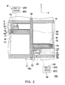
- FIG. 2 is a partial view of a pixel array according to the second embodiment of the invention.
- the pixel array 100 b of the present embodiment is similar to the pixel array 100 a of the first embodiment, their difference lies where the layout design of the thin-film transistor of the pixel array 100 b is different from the layout design of the thin-film transistor of the pixel array 100 a .
- components with same reference numerals represent same or similar components in the following embodiment, and the description to the same are omitted accordingly.
- the layout designs of the first thin-film transistor 112 and the second thin-film transistor 122 of the pixel array 100 b are described in detail as below.
- the first source electrode S 1 of the first thin-film transistor 112 of the present embodiment is composed by one conductor portion a, wherein the conductor portion a, for example, is an elongated conductor extended towards X direction.
- the first drain electrode D 1 is composed by one conductor portion b, wherein the conductor portion b, for example, is an elongated conductor extended towards X direction.
- the first source electrode S 1 is arranged parallel with the first drain electrode D 1 , and the length of the first drain electrode D 1 in the X direction is larger than the length of the first source electrode S 1 in the X direction, and an elongated gap is located between the first drain electrode D 1 and the first source electrode S 1 .
- the pattern and shape of the second thin-film transistor 122 and the pattern and shape of the first thin-film transistor 122 are substantially the same. Therefore, the orthogonal projection pattern of the first thin-film transistor 112 on the XY plane and the orthogonal projection pattern of the second thin-film transistor 122 on the XY plane are substantially the same.
- the orthogonal projection pattern of the first capacitance electrode 116 on the XY plane and the orthogonal projection pattern of the second capacitance electrode 126 on the XY plane are substantially the same.
- FIG. 3 is a partial view of a pixel array according to the third embodiment of the invention.
- the pixel array 100 c of the present embodiment is similar to the pixel array 100 a of the first embodiment, their difference lies where the layout design of the thin-film transistor of the pixel array 100 c is different from the layout design of the thin-film transistor of the pixel array 100 a .
- the layout designs of the first thin-film transistor 112 and the second thin-film transistor 122 of the pixel array 100 c are described in detail as below.
- the first source electrode S 1 of the first thin-film transistor 112 of the present embodiment is composed by one conductor portion a, wherein the conductor portion a is a U-shaped conductor having an opening towards X direction.
- the first drain electrode D 1 is composed by one conductor portion b, wherein the conductor portion b, for example, is an elongated conductor extended towards X direction.
- the first drain electrode D 1 is located within the opening of the first source electrode S 1 , and a U-shaped gap having an opening towards X direction is located between the first drain electrode D 1 and the first source electrode S 1 .
- the pattern and shape of the second thin-film transistor 122 and the pattern and shape of the first thin-film transistor 122 are substantially the same. Therefore, the orthogonal projection pattern of the first thin-film transistor 112 on XY plane and the orthogonal projection pattern of the second thin-film transistor 122 on XY plane are substantially the same.
- the orthogonal projection pattern of the first capacitance electrode 116 on XY plane and the orthogonal projection pattern of the second capacitance electrode 126 on XY plane are substantially the same.
- the patterns of the thin-film transistors as described in the first embodiment, the second embodiment and the third embodiment are illustrative examples only, the invention is not limited thereto.
- the orthogonal projection pattern of the first thin-film transistor on XY plane and the orthogonal projection pattern of the second thin-film transistor on XY plane are substantially the same in the same pixel unit, such pixel unit falls in the protection range which the invention intends to claim.
- FIG. 4 is a 3D exploded view of a display panel according to an embodiment of the invention.
- the display panel 10 of the present embodiment includes a first substrate 2 , a second substrate 4 and a display medium 6 .
- the second substrate 4 is located at the opposite side of the first substrate 2 .
- the display medium 6 is located between the first substrate 2 and the second substrate 4 .
- the second substrate 2 has a pixel array 100 a .
- the pixel array 100 a includes a plurality of pixel units 102 a.
- the second substrate 4 is a color filter substrate.
- the color filter substrate includes a substrate, a color filter layer, a protection layer and a common electrode (not illustrated).
- the display medium 6 is a liquid crystal layer.
- an electric field is formed between the pixel electrode (not illustrated) on the first substrate 2 and the common electrode (not illustrated) on the second substrate 4 , said electric field may be used for driving the liquid crystal molecules within the liquid crystal layer, such that the desired image may be displayed on the display panel 10 .
- the display panel 10 of the present embodiment includes said pixel array 100 a , the pixel array 100 a includes a plurality of pixel units 102 a .
- the pixel unit 102 a includes a first sub-pixel P 1 and a second sub-pixel P 2 , wherein the first sub-pixel P 1 includes a first scan line 110 , a data line 130 , a first thin-film transistor 112 , and a first pixel electrode 114 .
- the second sub-pixel P 2 includes a second scan line 120 , the data line 130 , a second thin-film transistor 122 and a second pixel electrode 124 .
- the orthogonal projection pattern of the first thin-film transistor 112 on the XY plane and the orthogonal projection pattern of the second thin-film transistor 122 on the XY plane are substantially the same.
- the display panel 10 since the display panel 10 includes the pixel array 100 a , and feed-through voltages of the first sub-pixel P 1 and the second sub-pixel P 2 in the pixel unit 102 a are the same. Therefore, during the operation of the display panel 10 , the desired image may be displayed on the display panel 10 with excellent display quality and without any flickering.
- the pixel array 100 a please refer back to the first embodiment above, it will not be described again hereinafter.
- the pixel array 100 a is selected as to describe the display panel 10 of the present embodiment. However, the invention is not limited thereto. In other embodiments which are not illustrated herein, the pixel array 100 b or the pixel array 100 c may also be selected as the pixel array used on the second substrate 2 of the display panel 10 .
- feed-through voltage is represented by V f .
- C lc represents the liquid crystal capacitance
- C st represents the pixel storage capacitance
- ⁇ V g represents the scan lines voltage difference between on and off states of the thin-film transistor.
- C gd is the parasitic capacitance between the gate electrode and the drain electrode of the thin-film transistor, the channel has an electric conductance property when the scan line turns on the thin-film transistor. Therefore, C gd may be affected by the overlapping area between the channel and the gate electrode.
- Table 1 is a comparison of pattern designs of the first thin-film transistor and the second thin-film transistor of the display panel, and pattern designs of the first capacitance electrode and the second capacitance electrode of the display panels in comparison example 1, comparison example 2, example 1 and example 2.
- the device performance of the display panel of the invention is described using testing result of, the deviation of the gate/drain parasitic capacitances ( ⁇ C gd ) between the first sub-pixel and the second sub-pixel, the deviation of storage capacitances ( ⁇ C st ) between the first sub-pixel and the second sub-pixel and the deviation of feed-through voltages ( ⁇ V f ) of the first sub-pixel and the second sub-pixel.
- Table 2 is the result of assessment to the display panels of comparison example 1, comparison example 2, example 1 and example 2.
- Pattern designs of the first thin-film transistor and the second thin-film transistor of the display panel in comparison example 2 are symmetrical in mirror, and pattern designs of the first capacitance electrode and the second capacitance electrode are completely the same, in which the deviation of feed-through voltages between the first sub-pixel and the second sub-pixel is 210 mV. Therefore, the voltages difference between the neighbouring sub-pixels of the display panel in comparison example 2 is approximately 10 gray scales.
- Pattern designs of the first thin-film transistor and the second thin-film transistor of the display panel in example 1 are completely the same, and pattern designs of the first capacitance electrode and the second capacitance electrode are only having the same area. Deviation of feed-through voltages between the first sub-pixel and the second sub-pixel of the display panel in example 1 is reduced to 20 mV. Therefore, the voltages difference between the neighbouring sub-pixels of the display panel in example 1 is improved to have only 1 gray scale difference, comparing to the display panels of comparison example 1 and comparison example 2. Accordingly, the same pattern designs of the first thin-film transistor and the second thin-film transistor may greatly reduce feed-through voltages difference between the neighbouring sub-pixels.
- pattern designs of the first thin-film transistor and the second thin-film transistor of the display panel in example 2 are completely the same, and pattern designs of the first capacitance electrode and the second capacitance electrode are completely the same, in which the deviation of feed-through voltages between the first sub-pixel and the second sub-pixel is 0 mV. Accordingly, the same pattern designs of the first thin-film transistor and the second thin-film transistor may further reduce feed-through voltages difference between the neighbouring sub-pixels, allowing the neighbouring sub-pixels to have substantially the same grey scale level, so that an excellent display quality may be obtained.
- the orthogonal projection patterns of the first thin-film transistor and the second thin-film transistor on XY plane are substantially the same, and the orthogonal projection patterns of the first capacitance electrode and the second capacitance electrode on XY plane are substantially the same. Accordingly, since overlay shifts of the first thin-film transistor and the second thin-film transistor are the same, the variations of gate/drain capacitance in the first thin-film transistor and the second thin-film transistor may be the same if overlay shift occurs during manufacturing process of the pixel array. As a result, feed-through voltages of the neighbouring sub-pixels in the same pixel may remain the same, thereby allowing the display panel to have a better display quality.
Landscapes
- Physics & Mathematics (AREA)
- Engineering & Computer Science (AREA)
- Nonlinear Science (AREA)
- Microelectronics & Electronic Packaging (AREA)
- General Physics & Mathematics (AREA)
- Power Engineering (AREA)
- Mathematical Physics (AREA)
- Chemical & Material Sciences (AREA)
- Crystallography & Structural Chemistry (AREA)
- Optics & Photonics (AREA)
- Computer Hardware Design (AREA)
- Condensed Matter Physics & Semiconductors (AREA)
- Liquid Crystal (AREA)
- Devices For Indicating Variable Information By Combining Individual Elements (AREA)
Priority Applications (1)
| Application Number | Priority Date | Filing Date | Title |
|---|---|---|---|
| US14/641,447 US9472580B2 (en) | 2012-03-30 | 2015-03-09 | Pixel array and display panel |
Applications Claiming Priority (3)
| Application Number | Priority Date | Filing Date | Title |
|---|---|---|---|
| TW101111419A TWI559046B (zh) | 2012-03-30 | 2012-03-30 | 畫素陣列及顯示面板 |
| TW101111419 | 2012-03-30 | ||
| TW101111419A | 2012-03-30 |
Related Child Applications (1)
| Application Number | Title | Priority Date | Filing Date |
|---|---|---|---|
| US14/641,447 Continuation US9472580B2 (en) | 2012-03-30 | 2015-03-09 | Pixel array and display panel |
Publications (2)
| Publication Number | Publication Date |
|---|---|
| US20130256706A1 US20130256706A1 (en) | 2013-10-03 |
| US9007541B2 true US9007541B2 (en) | 2015-04-14 |
Family
ID=46858339
Family Applications (2)
| Application Number | Title | Priority Date | Filing Date |
|---|---|---|---|
| US13/615,598 Active 2032-10-30 US9007541B2 (en) | 2012-03-30 | 2012-09-14 | Pixel array and display panel |
| US14/641,447 Active US9472580B2 (en) | 2012-03-30 | 2015-03-09 | Pixel array and display panel |
Family Applications After (1)
| Application Number | Title | Priority Date | Filing Date |
|---|---|---|---|
| US14/641,447 Active US9472580B2 (en) | 2012-03-30 | 2015-03-09 | Pixel array and display panel |
Country Status (3)
| Country | Link |
|---|---|
| US (2) | US9007541B2 (zh) |
| CN (1) | CN102692773B (zh) |
| TW (1) | TWI559046B (zh) |
Cited By (5)
| Publication number | Priority date | Publication date | Assignee | Title |
|---|---|---|---|---|
| US20150179671A1 (en) * | 2012-03-30 | 2015-06-25 | Au Optronics Corporation | Pixel array and display panel |
| US20160240601A1 (en) * | 2015-02-12 | 2016-08-18 | Samsung Display Co., Ltd. | Organic light emitting display apparatus |
| US10049626B2 (en) | 2016-01-04 | 2018-08-14 | Au Optronics Corporation | Pixel structure |
| US10331002B2 (en) * | 2017-03-31 | 2019-06-25 | Au Optronics Corporation | Pixel array substrate |
| US10559597B1 (en) * | 2018-09-30 | 2020-02-11 | Wuhan Tianma Micro-Electronics Co., Ltd. | Display panel and display device |
Families Citing this family (2)
| Publication number | Priority date | Publication date | Assignee | Title |
|---|---|---|---|---|
| TWI695205B (zh) * | 2018-08-10 | 2020-06-01 | 友達光電股份有限公司 | 影像感測顯示裝置以及影像處理方法 |
| TWI694427B (zh) * | 2019-02-27 | 2020-05-21 | 友達光電股份有限公司 | 顯示裝置 |
Citations (9)
| Publication number | Priority date | Publication date | Assignee | Title |
|---|---|---|---|---|
| US5191451A (en) * | 1990-04-20 | 1993-03-02 | Sharp Kabushiki Kaisha | Active matrix display device having drain electrodes of the pair of tfts being symmetrically formed with respect to the central plane to prevent the flicker due to the different parasitic capacitances |
| TW200628943A (en) | 2004-12-27 | 2006-08-16 | Samsung Electronics Co Ltd | Liquid crystal display |
| US20090190082A1 (en) * | 2008-01-25 | 2009-07-30 | Hong-Woo Lee | Display substrate, method of manufacturing the same and display panel having the display substrate |
| US7777851B2 (en) * | 2003-06-26 | 2010-08-17 | Lg. Display Co., Ltd. | Liquid crystal display device |
| US7791679B2 (en) * | 2003-06-06 | 2010-09-07 | Samsung Electronics Co., Ltd. | Alternative thin film transistors for liquid crystal displays |
| WO2010127515A1 (zh) | 2009-05-06 | 2010-11-11 | 深超光电(深圳)有限公司 | 显示面板 |
| US20110149184A1 (en) | 2009-12-18 | 2011-06-23 | Au Optronics Corporation | Pixel structure |
| TW201122691A (en) | 2009-12-31 | 2011-07-01 | Au Optronics Corp | Active device array substrate and fabricating mothod thereof |
| US20130105803A1 (en) * | 2011-10-31 | 2013-05-02 | Samsung Display Co., Ltd | Thin film transistor array panel |
Family Cites Families (7)
| Publication number | Priority date | Publication date | Assignee | Title |
|---|---|---|---|---|
| US5532180A (en) * | 1995-06-02 | 1996-07-02 | Ois Optical Imaging Systems, Inc. | Method of fabricating a TFT with reduced channel length |
| KR101067618B1 (ko) * | 2004-06-29 | 2011-09-27 | 엘지디스플레이 주식회사 | 액정표시패널 및 그 제조방법 |
| CN100483197C (zh) * | 2006-09-15 | 2009-04-29 | 友达光电股份有限公司 | 液晶显示器装置及其驱动方法 |
| KR101352113B1 (ko) * | 2007-05-17 | 2014-01-15 | 엘지디스플레이 주식회사 | 수평 전계 인가형 액정 표시 패널 및 그 제조방법 |
| CN101216649A (zh) * | 2008-01-10 | 2008-07-09 | 京东方科技集团股份有限公司 | 液晶显示装置阵列基板及驱动方法 |
| CN102231030B (zh) * | 2011-07-07 | 2013-04-10 | 南京中电熊猫液晶显示科技有限公司 | 薄膜晶体管液晶显示器的像素结构 |
| TWI559046B (zh) * | 2012-03-30 | 2016-11-21 | 友達光電股份有限公司 | 畫素陣列及顯示面板 |
-
2012
- 2012-03-30 TW TW101111419A patent/TWI559046B/zh active
- 2012-05-21 CN CN201210162133.XA patent/CN102692773B/zh active Active
- 2012-09-14 US US13/615,598 patent/US9007541B2/en active Active
-
2015
- 2015-03-09 US US14/641,447 patent/US9472580B2/en active Active
Patent Citations (13)
| Publication number | Priority date | Publication date | Assignee | Title |
|---|---|---|---|---|
| US5191451A (en) * | 1990-04-20 | 1993-03-02 | Sharp Kabushiki Kaisha | Active matrix display device having drain electrodes of the pair of tfts being symmetrically formed with respect to the central plane to prevent the flicker due to the different parasitic capacitances |
| US7791679B2 (en) * | 2003-06-06 | 2010-09-07 | Samsung Electronics Co., Ltd. | Alternative thin film transistors for liquid crystal displays |
| US7777851B2 (en) * | 2003-06-26 | 2010-08-17 | Lg. Display Co., Ltd. | Liquid crystal display device |
| TW200628943A (en) | 2004-12-27 | 2006-08-16 | Samsung Electronics Co Ltd | Liquid crystal display |
| US20090190082A1 (en) * | 2008-01-25 | 2009-07-30 | Hong-Woo Lee | Display substrate, method of manufacturing the same and display panel having the display substrate |
| US20100321602A1 (en) * | 2009-05-06 | 2010-12-23 | Chih-Chung Liu | Display panel |
| WO2010127515A1 (zh) | 2009-05-06 | 2010-11-11 | 深超光电(深圳)有限公司 | 显示面板 |
| US8223286B2 (en) | 2009-05-06 | 2012-07-17 | Century Display(ShenZhen)Co., Ltd. | Display panel |
| US20110149184A1 (en) | 2009-12-18 | 2011-06-23 | Au Optronics Corporation | Pixel structure |
| TW201122682A (en) | 2009-12-18 | 2011-07-01 | Au Optronics Corp | Pixel structure |
| US8289460B2 (en) | 2009-12-18 | 2012-10-16 | Au Optronics Corporation | Pixel structure |
| TW201122691A (en) | 2009-12-31 | 2011-07-01 | Au Optronics Corp | Active device array substrate and fabricating mothod thereof |
| US20130105803A1 (en) * | 2011-10-31 | 2013-05-02 | Samsung Display Co., Ltd | Thin film transistor array panel |
Non-Patent Citations (2)
| Title |
|---|
| "Office Action of China Counterpart Application", issued on Apr. 22, 2014, p. 1-8, in which the listed foreign reference (Ref. 1) was cited. |
| "Office Action of Taiwan Counterpart Application", issued on Jun. 11, 2014, p. 1-6, in which the listed foreign references(Ref. 2-3) were cited. |
Cited By (7)
| Publication number | Priority date | Publication date | Assignee | Title |
|---|---|---|---|---|
| US20150179671A1 (en) * | 2012-03-30 | 2015-06-25 | Au Optronics Corporation | Pixel array and display panel |
| US9472580B2 (en) * | 2012-03-30 | 2016-10-18 | Au Optronics Corporation | Pixel array and display panel |
| US20160240601A1 (en) * | 2015-02-12 | 2016-08-18 | Samsung Display Co., Ltd. | Organic light emitting display apparatus |
| US9842893B2 (en) * | 2015-02-12 | 2017-12-12 | Samsung Display Co., Ltd. | Organic light emitting display apparatus |
| US10049626B2 (en) | 2016-01-04 | 2018-08-14 | Au Optronics Corporation | Pixel structure |
| US10331002B2 (en) * | 2017-03-31 | 2019-06-25 | Au Optronics Corporation | Pixel array substrate |
| US10559597B1 (en) * | 2018-09-30 | 2020-02-11 | Wuhan Tianma Micro-Electronics Co., Ltd. | Display panel and display device |
Also Published As
| Publication number | Publication date |
|---|---|
| US20150179671A1 (en) | 2015-06-25 |
| CN102692773B (zh) | 2015-10-07 |
| US20130256706A1 (en) | 2013-10-03 |
| US9472580B2 (en) | 2016-10-18 |
| TW201339693A (zh) | 2013-10-01 |
| TWI559046B (zh) | 2016-11-21 |
| CN102692773A (zh) | 2012-09-26 |
Similar Documents
| Publication | Publication Date | Title |
|---|---|---|
| US9472580B2 (en) | Pixel array and display panel | |
| JP5269540B2 (ja) | 液晶表示装置 | |
| US10234740B2 (en) | Liquid crystal display device | |
| US9500922B2 (en) | Array substrate, liquid crystal display panel and display device | |
| US9105248B2 (en) | Array substrate, display device and method for driving pixels within each pixel region of the array substrate | |
| US20110285689A1 (en) | Display apparatus | |
| CN110488548B (zh) | 一种阵列基板和车载显示装置 | |
| US20170205673A1 (en) | Array substrate, display panel, display device and electronic device | |
| US8947472B2 (en) | Pixel array | |
| US8120720B2 (en) | Pixel structure | |
| JP2006276582A (ja) | 液晶表示装置 | |
| US8018399B2 (en) | Pixel array | |
| US7898630B2 (en) | Pixel structure | |
| US20050146645A1 (en) | Liquid crystal display device with a capacitance-compensated structure | |
| US10031378B2 (en) | Array substrate, display panel and display device | |
| US9691788B2 (en) | Display device | |
| US8724066B2 (en) | Liquid crystal display | |
| US6917407B2 (en) | Liquid crystal display device and method of fabricating the same | |
| US9563084B2 (en) | Liquid crystal display device and array substrate thereof | |
| US11906861B2 (en) | Display panel and display device | |
| JP2007183643A (ja) | 画素ユニットとそれを用いたディスプレイ装置 | |
| JP2008203676A (ja) | 液晶表示装置 | |
| US20240111196A1 (en) | Pixel structure and display panel | |
| US20160216572A1 (en) | Curved display device | |
| JP2009128739A (ja) | 液晶装置及び電子機器 |
Legal Events
| Date | Code | Title | Description |
|---|---|---|---|
| AS | Assignment |
Owner name: AU OPTRONICS CORPORATION, TAIWAN Free format text: ASSIGNMENT OF ASSIGNORS INTEREST;ASSIGNORS:CHEN, SZU-CHIEH;TING, YU-HSIN;CHEN, CHEN-MING;AND OTHERS;SIGNING DATES FROM 20120727 TO 20120907;REEL/FRAME:028975/0052 |
|
| STCF | Information on status: patent grant |
Free format text: PATENTED CASE |
|
| MAFP | Maintenance fee payment |
Free format text: PAYMENT OF MAINTENANCE FEE, 4TH YEAR, LARGE ENTITY (ORIGINAL EVENT CODE: M1551); ENTITY STATUS OF PATENT OWNER: LARGE ENTITY Year of fee payment: 4 |
|
| MAFP | Maintenance fee payment |
Free format text: PAYMENT OF MAINTENANCE FEE, 8TH YEAR, LARGE ENTITY (ORIGINAL EVENT CODE: M1552); ENTITY STATUS OF PATENT OWNER: LARGE ENTITY Year of fee payment: 8 |