US9001073B2 - Capacitance type touch panel and display device - Google Patents
Capacitance type touch panel and display device Download PDFInfo
- Publication number
- US9001073B2 US9001073B2 US13/465,055 US201213465055A US9001073B2 US 9001073 B2 US9001073 B2 US 9001073B2 US 201213465055 A US201213465055 A US 201213465055A US 9001073 B2 US9001073 B2 US 9001073B2
- Authority
- US
- United States
- Prior art keywords
- electrode
- end portion
- electrodes
- touch panel
- another end
- Prior art date
- Legal status (The legal status is an assumption and is not a legal conclusion. Google has not performed a legal analysis and makes no representation as to the accuracy of the status listed.)
- Active, expires
Links
Images


Classifications
-
- G—PHYSICS
- G06—COMPUTING; CALCULATING OR COUNTING
- G06F—ELECTRIC DIGITAL DATA PROCESSING
- G06F3/00—Input arrangements for transferring data to be processed into a form capable of being handled by the computer; Output arrangements for transferring data from processing unit to output unit, e.g. interface arrangements
- G06F3/01—Input arrangements or combined input and output arrangements for interaction between user and computer
- G06F3/03—Arrangements for converting the position or the displacement of a member into a coded form
- G06F3/041—Digitisers, e.g. for touch screens or touch pads, characterised by the transducing means
- G06F3/044—Digitisers, e.g. for touch screens or touch pads, characterised by the transducing means by capacitive means
- G06F3/0446—Digitisers, e.g. for touch screens or touch pads, characterised by the transducing means by capacitive means using a grid-like structure of electrodes in at least two directions, e.g. using row and column electrodes
-
- G—PHYSICS
- G06—COMPUTING; CALCULATING OR COUNTING
- G06F—ELECTRIC DIGITAL DATA PROCESSING
- G06F3/00—Input arrangements for transferring data to be processed into a form capable of being handled by the computer; Output arrangements for transferring data from processing unit to output unit, e.g. interface arrangements
- G06F3/01—Input arrangements or combined input and output arrangements for interaction between user and computer
- G06F3/03—Arrangements for converting the position or the displacement of a member into a coded form
- G06F3/041—Digitisers, e.g. for touch screens or touch pads, characterised by the transducing means
- G06F3/044—Digitisers, e.g. for touch screens or touch pads, characterised by the transducing means by capacitive means
- G06F3/0445—Digitisers, e.g. for touch screens or touch pads, characterised by the transducing means by capacitive means using two or more layers of sensing electrodes, e.g. using two layers of electrodes separated by a dielectric layer
-
- G—PHYSICS
- G06—COMPUTING; CALCULATING OR COUNTING
- G06F—ELECTRIC DIGITAL DATA PROCESSING
- G06F2203/00—Indexing scheme relating to G06F3/00 - G06F3/048
- G06F2203/041—Indexing scheme relating to G06F3/041 - G06F3/045
- G06F2203/04111—Cross over in capacitive digitiser, i.e. details of structures for connecting electrodes of the sensing pattern where the connections cross each other, e.g. bridge structures comprising an insulating layer, or vias through substrate
-
- H—ELECTRICITY
- H01—ELECTRIC ELEMENTS
- H01L—SEMICONDUCTOR DEVICES NOT COVERED BY CLASS H10
- H01L2924/00—Indexing scheme for arrangements or methods for connecting or disconnecting semiconductor or solid-state bodies as covered by H01L24/00
-
- H—ELECTRICITY
- H01—ELECTRIC ELEMENTS
- H01L—SEMICONDUCTOR DEVICES NOT COVERED BY CLASS H10
- H01L2924/00—Indexing scheme for arrangements or methods for connecting or disconnecting semiconductor or solid-state bodies as covered by H01L24/00
- H01L2924/0001—Technical content checked by a classifier
- H01L2924/0002—Not covered by any one of groups H01L24/00, H01L24/00 and H01L2224/00
Definitions
- the present invention relates to a capacitance type touch panel and a display device, and more particularly, to a technology effective for detecting disconnection of an X electrode or a Y electrode.
- a display device which includes a device for inputting information by a touch operation (contact press operation; hereinafter, simply referred to as touch) onto a display screen with the use of a user's finger or a pen (hereinafter, the device is referred to also as touch sensor or touch panel) is used for mobile electronic devices such as a PDA and a mobile terminal, various home electric appliances, an automated teller machine, and other such devices.
- touch operation contact press operation
- the touch panel there are known a resistive type touch panel that detects a change in resistance at a touched portion, a capacitance type touch panel that detects a change in capacitance, and an optical sensor type touch panel that detects a change in light intensity.
- the capacitance type touch panel is a touch panel disclosed in Japanese Patent Application Laid-open No. 2008-310550.
- vertical detection electrodes hereinafter, referred to as X electrodes
- horizontal detection electrodes hereinafter, referred to as Y electrodes
- the input processing portion detects the increase in capacitance, and calculates input coordinates based on a signal of the capacitance change detected by each electrode.
- one end portion of each of the X electrodes and the Y electrodes is connected to a wiring (hereinafter, referred to as extraction wiring), and the extraction wiring is connected to a terminal connected to a flexible wiring board, thereby supplying a drive voltage from one side of the Y electrode.
- extraction wiring a wiring (hereinafter, referred to as extraction wiring)
- the extraction wiring is connected to a terminal connected to a flexible wiring board, thereby supplying a drive voltage from one side of the Y electrode.
- a touch panel of this type is referred to as an end-fed type touch panel.
- an AC signal is applied from the Y electrode, and the AC signal is detected from each X electrode. Based on the detected AC signal, the disconnection of the X electrode, the disconnection of the Y electrode, and the short-circuit between the X electrode and the Y electrode are detected.
- the present invention has been made for solving the problem in the related art, and it is an object of the present invention to provide a technology for an end-fed capacitance type touch panel, which enables detection of a disconnection failure at the other end portion of an X electrode or a Y electrode without the need to bring a probe into direct contact with the other end portion of the X electrode or the Y electrode.
- a capacitance type touch panel includes: a substrate; X electrodes, which extend on the substrate in a second direction and are arranged in parallel in a first direction crossing the second direction; Y electrodes, which extend on the substrate in the first direction so as to cross each of the X electrodes and are arranged in parallel in the second direction; and extraction wirings, which are connected to one end portions of the Y electrodes, respectively, in which: each of the extraction wirings is connected to a terminal corresponding to the each of the extraction wiring, the terminal being formed at one side of the substrate; and, provided that adjacent two of the Y electrodes are a first Y electrode and a second Y electrode, another end portion of the first Y electrode and another end portion of the second Y electrode have a coupling capacitance for AC-coupling the another end portion of the first Y electrode and the another end portion of the second Y electrode.
- adjacent two of the X electrodes are a first X electrode and a second X electrode
- another end portion of the first X electrode and another end portion of the second X electrode have a coupling capacitance for AC-coupling the another end portion of the first X electrode and the another end portion of the second X electrode.
- a display device includes: a display panel; and the above-mentioned capacitance type touch panel, which is disposed on a viewer side of the display panel.
- detection of a disconnection failure at the other end portion of an X electrode or a Y electrode is enabled without the need to bring a probe into direct contact with the other end portion of the X electrode or the Y electrode.
- FIG. 1 is a diagram illustrating the electrode shape of a capacitance type touch panel behind the present invention
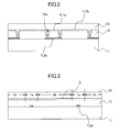
- FIG. 2 is a principal part cross-sectional view illustrating the structure of a capacitance type touch panel 1 behind the present invention, illustrating the cross-sectional structure taken along the line II-II of FIG. 1 ;
- FIG. 3 is a principal part cross-sectional view illustrating the structure of the capacitance type touch panel 1 behind the present invention, illustrating the cross-sectional structure taken along the line III-III of FIG. 1 ;
- FIG. 4 is a principal part cross-sectional view illustrating the structure of a capacitance type touch panel 2 behind the present invention, illustrating the cross-sectional structure taken along the same line as FIG. 2 ;
- FIG. 5 is a principal part cross-sectional view illustrating the structure of the capacitance type touch panel 2 behind the present invention, illustrating the cross-sectional structure taken along the same line as FIG. 3 ;
- FIG. 6 is a diagram illustrating the problem of the capacitance type touch panels 1 and 2 behind the present invention.
- FIG. 7 is a diagram illustrating the electrode shape of a capacitance type touch panel according to a first embodiment of the present invention.
- FIG. 8 is a principal part cross-sectional view illustrating the cross-sectional structure taken along the line VIII-VIII of FIG. 7 ;
- FIG. 9 is a principal part cross-sectional view illustrating a capacitance type touch panel according to a second embodiment of the present invention, illustrating the cross-sectional structure taken along the same line as FIG. 8 ;
- FIG. 10 is a principal part cross-sectional view illustrating a capacitance type touch panel according to a third embodiment of the present invention, illustrating the cross-sectional structure taken along the same line as FIG. 8 ;
- FIG. 11 is a principal part cross-sectional view illustrating a capacitance type touch panel according to a fourth embodiment of the present invention, illustrating the cross-sectional structure taken along the same line as FIG. 8 ;
- FIG. 12 is a principal part cross-sectional view illustrating a capacitance type touch panel according to a fifth embodiment of the present invention, illustrating the cross-sectional structure taken along the same line as FIG. 8 ;
- FIG. 13 is a diagram illustrating the electrode shape of a capacitance type touch panel according to a sixth embodiment of the present invention.
- FIG. 14 is a diagram illustrating the electrode shape of a modified example of the capacitance type touch panel according to the sixth embodiment of the present invention.
- FIG. 15 is a diagram illustrating the electrode shape of another modified example of the capacitance type touch panel according to the sixth embodiment of the present invention.
- FIG. 1 is a diagram illustrating the electrode shape of a capacitance type touch panel behind the present invention.
- the touch panel behind the present invention includes X electrodes (X 1 to X 5 ) and Y electrodes (Y 1 to Y 6 ).
- the X electrodes (X 1 to X 5 ) extend in a second direction (Y direction) and are arranged in parallel at a predetermined array pitch in a first direction (X direction) crossing the second direction.
- the Y electrodes (Y 1 to Y 6 ) extend in the first direction while crossing the X electrodes and are arranged in parallel at a predetermined array pitch in the second direction.
- a portion indicated by a dotted frame of FIG. 1 is an effective touch region (ART).
- One end portions of the X electrodes (X 1 to X 5 ) are respectively connected to extraction wirings (LX 1 to LX 5 ), and the extraction wirings (LX 1 to LX 5 ) are respectively connected to terminals (TX 1 to TX 5 ) formed at one side of a substrate 11 .
- one end portions of the Y electrodes (Y 1 to Y 6 ) are respectively connected to extraction wirings (LY 1 to LY 6 ), and the extraction wirings (LY 1 to LY 6 ) are respectively connected to terminals (TY 1 to TY 6 ) formed at the one side of the substrate 11 .
- Each of the X electrodes (X 1 to X 5 ) has an electrode pattern in which thin portions 1 a and pad portions 1 b , which have a larger width than the thin portions 1 a , are disposed alternately in the second direction.
- Each of the Y electrodes (Y 1 to Y 6 ) has an electrode pattern in which thin portions 2 a and pad portions 2 b , which have a larger width than the thin portions 2 a , are disposed alternately in the first direction.
- FIGS. 2 and 3 are principal part cross-sectional views illustrating the capacitance type touch panel 1 behind the present invention.
- FIG. 2 is a principal part cross-sectional view illustrating the cross-sectional structure taken along the line II-II of FIG. 1 .
- FIG. 3 is a principal part cross-sectional view illustrating the cross-sectional structure taken along the line III-III of FIG. 1 .
- the X electrodes (X 1 to X 5 ) are disposed on an insulating film 12 and covered by a protective film 13 formed thereon.
- each of the X electrodes (X 1 to X 5 ) has the electrode pattern in which the thin portions 1 a and the pad portions 1 b , which have a larger width than the thin portions 1 a , are disposed alternately in the second direction.
- each of the Y electrodes (Y 1 to Y 6 ) has the electrode pattern in which the thin portions 2 a and the pad portions 2 b , which have a larger width than the thin portions 2 a , are disposed alternately in the first direction.
- the pad portion 1 b of each of the X electrodes and the pad portion 2 b of each of the Y electrodes are disposed so as not to overlap each other.
- the thin portion 2 a of each of the Y electrodes (Y 1 to Y 6 ) is disposed on the substrate 11 and crosses the thin portion 1 a of the X electrode in plan view.
- the pad portion 2 b of each of the Y electrodes (Y 1 to Y 6 ) is disposed on the insulating film 12 similarly to the thin portion 1 a and the pad portion 1 b of the X electrode, and is formed so as to be separated from the pad portion 1 b of the X electrode.
- the pad portion 2 b of each of the Y electrodes (Y 1 to Y 6 ) is covered by the protective film 13 similarly to the X electrode.
- the thin portion 2 a of the Y electrode which is formed on the substrate 11 , is electrically connected to two pad portions 2 b , which are adjacent across the thin portion 2 a , via contact holes 12 a formed in the insulating film 12 .
- a transparent insulating substrate such as glass is used as the substrate 11 .
- the X electrodes and the Y electrodes are formed of a material having high transmission property, for example, a transparent conductive material such as indium tin oxide (ITO).
- FIGS. 4 and 5 are principal part cross-sectional views illustrating a capacitance type touch panel 2 behind the present invention.
- FIG. 4 is a principal part cross-sectional view illustrating the cross-sectional structure taken along the same line as FIG. 2 .
- FIG. 5 is a principal part cross-sectional view illustrating the cross-sectional structure taken along the same line as FIG. 3 .
- the touch panel 2 behind the present invention is different from the touch panel 1 behind the present invention in that the pad portion 2 b of each of the X electrodes (X 1 to X 5 ) and the pad portion 2 b of each of the Y electrodes (Y 1 to Y 6 ) are formed on the substrate 11 .
- the X electrodes (X 1 to X 5 ) are disposed on the substrate 11 .
- the pad portion 1 b of each of the X electrodes and the pad portion 2 b of each of the Y electrodes are disposed so as not to overlap each other, and the thin portion 1 a of each of the X electrodes and the thin portion 2 a of each of the Y electrodes cross each other.
- the pad portion 2 b of each of the Y electrodes (Y 1 to Y 6 ) is formed on the substrate 11 so as to be separated from the pad portion 1 b of the X electrode.
- the thin portion 2 a of each of the Y electrodes (Y 1 to Y 6 ) is disposed on the insulating film 12 and covered by the protective film 13 .
- the thin portion 2 a of the Y electrode is electrically connected to two pad portions 2 b , which are adjacent across the thin portion 2 a , via the contact holes 12 a formed in the insulating film 12 .
- an AC signal is applied from the Y electrode, and the AC signal is detected from each X electrode. Based on the detected AC signal, the disconnection of the X electrodes (X 1 to X 5 ), the disconnection of the Y electrodes (Y 1 to Y 6 ), and the short-circuit between the X electrodes (X 1 to X 5 ) and the Y electrodes (Y 1 to Y 6 ) are detected.
- the disconnection portion (DSE) cannot be discovered by the above-mentioned method. As a result, the touch at this portion cannot be detected. The same applies to the end portion of the X electrode.
- FIG. 6 is a diagram illustrating the problem of the capacitance type touch panels 1 and 2 behind the present invention.
- FIG. 7 is a diagram illustrating the electrode shape of a capacitance type touch panel according to a first embodiment of the present invention. Note that, FIG. 7 illustrates only a part in which the X electrodes X 1 and X 2 cross the Y electrodes Y 6 and Y 5 .
- FIG. 8 is a principal part cross-sectional view illustrating the cross-sectional structure taken along the line VIII-VIII of FIG. 7 .
- the conductive layer 16 overlaps a pad portion (X 1 - b E) of the end portion of the X electrode (X 1 ) and a pad portion (X 2 - b E) of the end portion of the X electrode (X 2 ) in a region outside the effective touch region
- the conductive layer 17 overlaps a pad portion (Y 5 - b E) of the end portion of the Y electrode (Y 5 ) and the other pad portion (Y 6 - b E) of the Y electrode (Y 6 ) in a region outside the effective touch region.
- the structure of the touch panel of this embodiment is the same as that of the touch panel 2 described with reference to FIGS. 4 and 5 , and the conductive layer ( 16 , 17 ) is formed on the insulating film 12 .
- the conductive layer ( 16 , 17 ) is formed of a metal layer or ITO, and, if formed of the same material as that of the thin portion ( 2 a ) of the Y electrode, the conductive layer ( 16 , 17 ) can be produced by the same process as the thin portion ( 2 a ) of the Y electrode.
- an AC signal is input from the Y electrode Y 6 , and the AC signal is detected from the Y electrode Y 5 via a coupling capacitance formed between the pad portion (Y 5 - b E) of the end portion of the Y electrode (Y 5 ) and the conductive layer 17 and a coupling capacitance formed between the other pad portion (Y 6 - b E) of the Y electrode (Y 6 ) and the conductive layer 17 .
- the disconnection at the end portion of the Y electrode (Y 5 ), the disconnection at the end portion of the Y electrode (Y 6 ), and the short-circuit between the end portion of the Y electrode (Y 5 ) and the end portion of the Y electrode (Y 6 ) can be detected.
- an AC signal is input from the X electrode X 1 , and the AC signal is detected from the X electrode X 2 via a coupling capacitance formed between the pad portion (X 1 - b E) of the end portion of the X electrode (X 1 ) and the conductive layer 16 and a coupling capacitance formed between the other pad portion (X 2 - b E) of the X electrode (X 2 ) and the conductive layer 16 .
- the disconnection at the end portion of the X electrode (X 1 ), the disconnection at the end portion of the X electrode (X 2 ), and the short-circuit between the end portion of the X electrode (X 1 ) and the end portion of the X electrode (X 2 ) can be detected.
- a drive voltage is sequentially input from the Y electrodes, and the touch position of the touch panel is detected based on signals detected at the X electrodes (X 1 to X 5 ). Therefore, even in the period for detecting the touch position, the drive voltage input from the Y electrode is also input, via the coupling capacitance formed between the pad portion of the end portion of the Y electrode and the conductive layer 17 , to Y electrodes other than the Y electrode to which the drive voltage is input, and the drive voltage is then output to the X electrodes (X 1 to X 5 ). As a result, there is a possibility that the touch position of the touch panel is erroneously identified.
- the coupling capacitance formed between the pad portion of the end portion of the Y electrode and the conductive layer 17 and the coupling capacitance formed between the pad portion of the end portion of the X electrode and the conductive layer 16 need to be set to such a value that does not cause a malfunction of the touch position detection in the normal touch position detection period.
- FIG. 9 is a principal part cross-sectional view illustrating a capacitance type touch panel according to a second embodiment of the present invention.
- FIG. 9 illustrates a cross-sectional structure taken along the same line as FIG. 8 .
- the structure of the touch panel of this embodiment is the same as that of the touch panel 2 described with reference to FIGS. 2 and 3 .
- the conductive layer 17 is formed on the substrate 11 .
- the above-mentioned conductive layer 16 is also formed on the substrate 11 .
- the conductive layer ( 16 , 17 ) is formed of a metal layer or ITO, and, if formed of the same material as that of the thin portion ( 2 a ) of the Y electrode, the conductive layer ( 16 , 17 ) can be produced by the same process as the thin portion ( 2 a ) of the Y electrode.
- the conductive layer 17 does not overlap the pad portions of the end portions of all the Y electrodes, but the conductive layers 17 are provided so as to overlap the end portions of adjacent two Y electrodes every adjacent two Y electrodes.
- the plurality of (two in FIG. 9 ) conductive layers 17 are provided so as to overlap the pad portion of the end portion of the Y electrode (Y 5 ) and the other pad portion of the Y electrode (Y 6 ) and overlap the pad portion of the end portion of the Y electrode (Y 3 ) and the other pad portion of the Y electrode (Y 4 ) in a region outside the effective touch region.
- the conductive layer 16 on the X electrode side does not overlap the pad portions of the end portions of all the X electrodes, either, but the conductive layers 16 are provided so as to overlap the end portions of adjacent two X electrodes every adjacent two X electrodes.
- the conductive layers 16 on the X electrode side or the conductive layers 17 on the Y electrode side may be provided every adjacent two or more X electrodes or adjacent two or more Y electrodes, instead of being provided every adjacent two X electrodes or adjacent two Y electrodes. Also in this embodiment, the same function and effect as those of the above-mentioned first embodiment can be obtained.
- FIG. 10 is a principal part cross-sectional view illustrating a capacitance type touch panel according to a third embodiment of the present invention.
- FIG. 10 illustrates a cross-sectional structure taken along the same line as FIG. 8 .
- the touch panel of this embodiment is modified from the structure of FIG. 8 so that the conductive layer 17 is electrically connected to the Y electrode Y 5 .
- an AC signal is input from the Y electrode Y 6 , and the AC signal is detected from the Y electrode Y 5 via a coupling capacitance formed between the pad portion (Y 6 - b E) of the end portion of the Y electrode (Y 6 ) and the conductive layer 17 .
- the disconnection at the end portion of the Y electrode (Y 5 ) the disconnection at the end portion of the Y electrode (Y 6 ), and the short-circuit between the end portion of the Y electrode (Y 5 ) and the end portion of the Y electrode (Y 6 ).
- the conductive layer 16 on the X electrode side is also electrically connected to an arbitrary X electrode similarly to FIG. 10 .
- FIG. 11 is a principal part cross-sectional view illustrating a capacitance type touch panel according to a fourth embodiment of the present invention.
- FIG. 11 illustrates a cross-sectional structure taken along the same line as FIG. 8 .
- the touch panel of this embodiment is modified from the structure of FIG. 9 so that two conductive layers 17 are electrically connected to the Y electrodes Y 3 and Y 5 , respectively.
- the conductive layers 16 on the X electrode side are also electrically connected to arbitrary X electrodes similarly to FIG. 11 . Also in this embodiment, the same function and effect as those of the above-mentioned first embodiment can be obtained.
- FIG. 12 is a principal part cross-sectional view illustrating a capacitance type touch panel according to a fifth embodiment of the present invention.
- FIG. 12 illustrates a cross-sectional structure taken along the same line as FIG. 8 .
- the touch panel of this embodiment is modified from the structure of FIG. 8 so that the conductive layers 17 are formed on the rear side of the substrate 11 so as to overlap the end portions of adjacent two Y electrodes every adjacent two Y electrodes.
- the conductive layers 16 on the X electrode side are also formed on the rear side of the substrate 11 so as to overlap the end portions of adjacent two X electrodes every adjacent two X electrodes similarly to FIG. 12 . Also in this embodiment, the same function and effect as those of the above-mentioned first embodiment can be obtained.
- the conductive layer 16 on the X electrode side and the pad portion of the end portion of the X electrode, and the conductive layer 17 on the Y electrode side and the pad portion of the end portion of the Y electrode do not always need to overlap each other in a region outside the effective touch region.
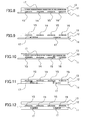
- FIG. 13 is a diagram illustrating the electrode shape of a capacitance type touch panel according to a sixth embodiment of the present invention. Note that, FIG. 13 illustrates only a part in which the X electrodes X 1 and X 2 cross the Y electrodes Y 6 and Y 5 .
- the pad portion (X 2 - b E) of the end portion of the X electrode X 2 is extended to form an extended pattern portion 19 .
- a coupling capacitance is formed between the extended pattern portion 19 and the pad portion (X 1 - b E) of the end portion of the X electrode X 1 , thereby AC-coupling the pad portion (X 2 - b E) of the end portion of the X electrode X 2 and the pad portion (X 1 - b E) of the end portion of the X electrode X 1 .
- the pad portion (Y 6 - b E) of the end portion of the Y electrode Y 6 is extended to form an extended pattern portion 20 .
- a coupling capacitance is formed between the extended pattern portion 20 and the pad portion (Y 5 - b E) of the end portion of the Y electrode Y 5 , thereby AC-coupling the pad portion (Y 6 - b E) of the end portion of the Y electrode Y 6 and the pad portion (Y 5 - b E) of the end portion of the Y electrode Y 5 .
- FIG. 14 is a diagram illustrating the electrode shape of a modified example of the capacitance type touch panel according to the sixth embodiment of the present invention. Note that, FIG. 14 illustrates only a part in which the X electrodes X 1 and X 2 cross the Y electrodes Y 6 and Y 5 .
- the pad portion (X 1 - b E) of the end portion of the X electrode X 1 is extended to form an extended pattern portion 19 b
- the pad portion (X 2 - b E) of the end portion of the X electrode X 2 is extended to form an extended pattern portion 19 a .
- a coupling capacitance is formed between the extended pattern portion 19 a and the pad portion (X 1 - b E) of the end portion of the X electrode X 1 , between the extended pattern portion 19 b and the pad portion (X 2 - b E) of the end portion of the X electrode X 2 , and between the extended pattern portion 19 a and the extended pattern portion 19 b , thereby AC-coupling the pad portion (X 2 - b E) of the end portion of the X electrode X 2 and the pad portion (X 1 - b E) of the end portion of the X electrode X 1 .
- the pad portion (Y 5 - b E) of the end portion of the Y electrode Y 5 is extended to form an extended pattern portion 20 b
- the pad portion (Y 6 - b E) of the end portion of the X electrode Y 6 is extended to form an extended pattern portion 20 a .
- a coupling capacitance is formed between the extended pattern portion 20 a and the pad portion (Y 5 - b E) of the end portion of the Y electrode Y 5 , between the extended pattern portion 20 b and the pad portion (Y 6 - b E) of the end portion of the Y electrode Y 6 , and between the extended pattern portion 20 a and the extended pattern portion 20 b , thereby AC-coupling the pad portion (Y 6 - b E) of the end portion of the Y electrode Y 6 and the pad portion (Y 5 - b E) of the end portion of the Y electrode Y 5 .
- FIG. 15 is a diagram illustrating the electrode shape of another modified example of the capacitance type touch panel according to the sixth embodiment of the present invention. Note that, FIG. 15 illustrates only a part in which the X electrodes X 1 and X 2 cross the Y electrodes Y 6 and Y 5 .
- an extended pattern portion 21 is formed so as to protrude from the pad portion (X 2 - b E) of the end portion of the X electrode X 2 .
- a coupling capacitance is formed between the extended pattern portion 21 and the pad portion (X 1 - b E) of the end portion of the X electrode X 1 , thereby AC-coupling the pad portion (X 2 - b E) of the end portion of the X electrode X 2 and the pad portion (X 1 - b E) of the end portion of the X electrode X 1 .
- an extended pattern portion 22 is formed so as to protrude from the pad portion (Y 6 - b E) of the end portion of the Y electrode Y 6 .
- a coupling capacitance is formed between the extended pattern portion 22 and the pad portion (Y 5 - b E) of the end portion of the Y electrode Y 5 , thereby AC-coupling the pad portion (Y 6 - b E) of the end portion of the Y electrode Y 6 and the pad portion (Y 5 - b E) of the end portion of the Y electrode Y 5 .
Applications Claiming Priority (2)
| Application Number | Priority Date | Filing Date | Title |
|---|---|---|---|
| JP2011105064A JP2012238066A (ja) | 2011-05-10 | 2011-05-10 | 静電容量方式のタッチパネル、および表示装置 |
| JP2011-105064 | 2011-05-10 |
Publications (2)
| Publication Number | Publication Date |
|---|---|
| US20120287079A1 US20120287079A1 (en) | 2012-11-15 |
| US9001073B2 true US9001073B2 (en) | 2015-04-07 |
Family
ID=47141568
Family Applications (1)
| Application Number | Title | Priority Date | Filing Date |
|---|---|---|---|
| US13/465,055 Active 2032-06-11 US9001073B2 (en) | 2011-05-10 | 2012-05-07 | Capacitance type touch panel and display device |
Country Status (5)
| Country | Link |
|---|---|
| US (1) | US9001073B2 (ja) |
| JP (1) | JP2012238066A (ja) |
| KR (1) | KR101386306B1 (ja) |
| CN (1) | CN102819368B (ja) |
| TW (1) | TWI604580B (ja) |
Cited By (1)
| Publication number | Priority date | Publication date | Assignee | Title |
|---|---|---|---|---|
| US11644869B2 (en) | 2014-05-30 | 2023-05-09 | Semiconductor Energy Laboratory Co., Ltd. | Touch panel comprising conductive layers having opening overlapping with light-emitting element |
Families Citing this family (9)
| Publication number | Priority date | Publication date | Assignee | Title |
|---|---|---|---|---|
| KR102149498B1 (ko) * | 2013-09-24 | 2020-09-01 | 삼성디스플레이 주식회사 | 터치 스크린 패널 |
| KR102161743B1 (ko) | 2013-11-26 | 2020-10-06 | 삼성디스플레이 주식회사 | 터치 감지 장치 및 이를 포함하는 표시 장치 |
| US20160147323A1 (en) * | 2014-11-21 | 2016-05-26 | Interface Optoelectronics Corporation | Touch control panel structure and method of manufacturing the same |
| CN107728861B (zh) * | 2016-08-10 | 2021-09-14 | 深圳莱宝高科技股份有限公司 | 电容式触控面板 |
| JP2018036896A (ja) * | 2016-08-31 | 2018-03-08 | 株式会社ジャパンディスプレイ | タッチセンサ及び表示装置 |
| KR102075065B1 (ko) * | 2017-02-16 | 2020-02-07 | 동우 화인켐 주식회사 | 터치 센서 및 이의 제조 방법 |
| JP6721667B2 (ja) * | 2018-12-19 | 2020-07-15 | Nissha株式会社 | タッチパネル、タッチパネルモジュールおよびタッチパネルの検査方法 |
| CN114051604B (zh) * | 2019-08-07 | 2024-04-30 | 松下知识产权经营株式会社 | 触摸传感器 |
| CN110515492B (zh) * | 2019-08-28 | 2023-05-02 | 武汉天马微电子有限公司 | 一种显示模组及其检测方法和显示装置 |
Citations (11)
| Publication number | Priority date | Publication date | Assignee | Title |
|---|---|---|---|---|
| CN1287650A (zh) | 1998-10-16 | 2001-03-14 | 精工爱普生株式会社 | 电光装置用基板和有源矩阵基板以及电光装置用基板的检查方法 |
| CN1576870A (zh) | 2003-07-04 | 2005-02-09 | 株式会社东京阴极研究所 | 导电图案检查装置 |
| US6947853B2 (en) * | 2002-05-23 | 2005-09-20 | Oht, Inc. | Apparatus and method for inspecting electrical continuity of circuit board, jig for use therein, and recording medium thereon |
| US20070057344A1 (en) * | 2005-09-13 | 2007-03-15 | Via Technologies, Inc. | Embedded capacitor with interdigitated structure |
| US20080309635A1 (en) | 2007-06-14 | 2008-12-18 | Epson Imaging Devices Corporation | Capacitive input device |
| CN101546243A (zh) | 2008-03-26 | 2009-09-30 | 爱普生映像元器件有限公司 | 静电电容式输入装置、带输入功能的显示装置及电子设备 |
| US20100182275A1 (en) * | 2009-01-20 | 2010-07-22 | Hitachi Displays, Ltd. | Display device |
| US7859039B2 (en) * | 2006-06-16 | 2010-12-28 | Realtek Semiconductor Corp. | X-shaped semiconductor capacitor structure |
| US20100328562A1 (en) * | 2009-06-25 | 2010-12-30 | Chin-Hai Huang | Liquid crystal display panel |
| US20100328255A1 (en) * | 2009-06-30 | 2010-12-30 | Sony Corporation | Touch detection device and display device having touch sensor function |
| KR20110083196A (ko) | 2010-01-14 | 2011-07-20 | 마이크로 인스펙션 주식회사 | 터치패널의 검사장치 |
Family Cites Families (7)
| Publication number | Priority date | Publication date | Assignee | Title |
|---|---|---|---|---|
| JP2002365325A (ja) * | 2001-06-11 | 2002-12-18 | Oht Inc | 回路パターン検査装置並びに回路パターン検査方法及び記録媒体 |
| JP5391819B2 (ja) * | 2009-05-14 | 2014-01-15 | 日本電産リード株式会社 | タッチパネル検査装置 |
| CN201413440Y (zh) * | 2009-06-12 | 2010-02-24 | 华映视讯(吴江)有限公司 | 能测试液晶单元缺陷、点线缺陷和配线缺陷的液晶显示面板 |
| JP5300640B2 (ja) * | 2009-07-27 | 2013-09-25 | 株式会社ジャパンディスプレイウェスト | 静電容量型入力装置および入力装置付き電気光学装置 |
| CN101699376B (zh) * | 2009-09-04 | 2011-09-14 | 深超光电(深圳)有限公司 | 触控面板及触控面板的检测方法 |
| JP5443251B2 (ja) * | 2010-04-21 | 2014-03-19 | 株式会社ジャパンディスプレイ | タッチパネル、および表示装置 |
| CN201716708U (zh) * | 2010-07-14 | 2011-01-19 | 敏理投资股份有限公司 | 触控面板 |
-
2011
- 2011-05-10 JP JP2011105064A patent/JP2012238066A/ja not_active Withdrawn
-
2012
- 2012-05-02 TW TW101115652A patent/TWI604580B/zh active
- 2012-05-07 US US13/465,055 patent/US9001073B2/en active Active
- 2012-05-09 KR KR1020120048942A patent/KR101386306B1/ko active IP Right Grant
- 2012-05-09 CN CN201210150250.4A patent/CN102819368B/zh active Active
Patent Citations (12)
| Publication number | Priority date | Publication date | Assignee | Title |
|---|---|---|---|---|
| CN1287650A (zh) | 1998-10-16 | 2001-03-14 | 精工爱普生株式会社 | 电光装置用基板和有源矩阵基板以及电光装置用基板的检查方法 |
| US6947853B2 (en) * | 2002-05-23 | 2005-09-20 | Oht, Inc. | Apparatus and method for inspecting electrical continuity of circuit board, jig for use therein, and recording medium thereon |
| CN1576870A (zh) | 2003-07-04 | 2005-02-09 | 株式会社东京阴极研究所 | 导电图案检查装置 |
| US20070057344A1 (en) * | 2005-09-13 | 2007-03-15 | Via Technologies, Inc. | Embedded capacitor with interdigitated structure |
| US7859039B2 (en) * | 2006-06-16 | 2010-12-28 | Realtek Semiconductor Corp. | X-shaped semiconductor capacitor structure |
| US20080309635A1 (en) | 2007-06-14 | 2008-12-18 | Epson Imaging Devices Corporation | Capacitive input device |
| JP2008310550A (ja) | 2007-06-14 | 2008-12-25 | Epson Imaging Devices Corp | 静電容量型入力装置 |
| CN101546243A (zh) | 2008-03-26 | 2009-09-30 | 爱普生映像元器件有限公司 | 静电电容式输入装置、带输入功能的显示装置及电子设备 |
| US20100182275A1 (en) * | 2009-01-20 | 2010-07-22 | Hitachi Displays, Ltd. | Display device |
| US20100328562A1 (en) * | 2009-06-25 | 2010-12-30 | Chin-Hai Huang | Liquid crystal display panel |
| US20100328255A1 (en) * | 2009-06-30 | 2010-12-30 | Sony Corporation | Touch detection device and display device having touch sensor function |
| KR20110083196A (ko) | 2010-01-14 | 2011-07-20 | 마이크로 인스펙션 주식회사 | 터치패널의 검사장치 |
Non-Patent Citations (1)
| Title |
|---|
| English translation of communication issued in connection with corresponding Chinese Patent Application No. 2012/10150250.4, mailed Oct. 10, 2014. |
Cited By (1)
| Publication number | Priority date | Publication date | Assignee | Title |
|---|---|---|---|---|
| US11644869B2 (en) | 2014-05-30 | 2023-05-09 | Semiconductor Energy Laboratory Co., Ltd. | Touch panel comprising conductive layers having opening overlapping with light-emitting element |
Also Published As
| Publication number | Publication date |
|---|---|
| US20120287079A1 (en) | 2012-11-15 |
| TWI604580B (zh) | 2017-11-01 |
| JP2012238066A (ja) | 2012-12-06 |
| TW201301458A (zh) | 2013-01-01 |
| CN102819368B (zh) | 2015-12-16 |
| KR101386306B1 (ko) | 2014-04-17 |
| CN102819368A (zh) | 2012-12-12 |
| KR20120126022A (ko) | 2012-11-20 |
Similar Documents
| Publication | Publication Date | Title |
|---|---|---|
| US9001073B2 (en) | Capacitance type touch panel and display device | |
| US8704796B2 (en) | Touch panel and display device | |
| US8654090B2 (en) | Touch panel and display device | |
| US9176611B2 (en) | Touch screen panel including a plurality of relay patterns and an auxiliary pattern | |
| KR101322998B1 (ko) | 정전용량 방식 터치 스크린 패널 | |
| US9798419B2 (en) | Electrostatic capacitive type touch screen panel | |
| KR20140051649A (ko) | 메탈 메쉬형 터치 스크린 패널 | |
| JP2012089102A (ja) | 静電容量式タッチスクリーン及びその製造方法 | |
| US10359879B2 (en) | Touch control display panel and display device | |
| KR20150009420A (ko) | 터치 윈도우 | |
| KR20150072838A (ko) | 터치패널 | |
| JP2012059247A (ja) | 静電容量式タッチスクリーン及びその製造方法 | |
| KR102119827B1 (ko) | 터치 패널 | |
| US8780067B1 (en) | Bridging structure for signal transmission of touch panel | |
| KR101260726B1 (ko) | 간섭 없이 감도가 향상되는 단일 적층 구조를 갖는 터치스크린 패널 | |
| CN105320374A (zh) | 触摸屏及其制造方法 | |
| KR102262553B1 (ko) | 터치 패널 | |
| KR102585123B1 (ko) | 표시 장치 | |
| US9342171B2 (en) | Touch panel with first and second electrodes extending in the same direction but on opposite surfaces of a substrate | |
| JP6290271B2 (ja) | インセル型タッチ表示パネル | |
| JP2021125158A (ja) | タッチパネルおよびこれを備えた表示装置 | |
| US9195277B2 (en) | Touch panel with proximity sensor | |
| KR101323048B1 (ko) | 표시장치용 정전용량식 터치 감지 패널 | |
| JP3213947U (ja) | 静電容量式タッチスイッチ電極 | |
| US20130342503A1 (en) | Signal Enhancing Method for Capacitive Touch Panel of Mobile Device |
Legal Events
| Date | Code | Title | Description |
|---|---|---|---|
| AS | Assignment |
Owner name: HITACHI DISPLAYS, LTD., JAPAN Free format text: ASSIGNMENT OF ASSIGNORS INTEREST;ASSIGNORS:SATO, TAKUMI;TERAMOTO, MASAHIRO;ANNO, KOUICHI;SIGNING DATES FROM 20120319 TO 20120404;REEL/FRAME:028162/0706 |
|
| AS | Assignment |
Owner name: JAPAN DISPLAY INC., JAPAN Free format text: CHANGE OF NAME;ASSIGNOR:JAPAN DISPLAY EAST, INC.;REEL/FRAME:032387/0066 Effective date: 20130401 Owner name: JAPAN DISPLAY EAST, INC., JAPAN Free format text: CHANGE OF NAME;ASSIGNOR:HITACHI DISPLAYS, LTD.;REEL/FRAME:032387/0001 Effective date: 20120401 |
|
| FEPP | Fee payment procedure |
Free format text: PAYOR NUMBER ASSIGNED (ORIGINAL EVENT CODE: ASPN); ENTITY STATUS OF PATENT OWNER: LARGE ENTITY |
|
| STCF | Information on status: patent grant |
Free format text: PATENTED CASE |
|
| MAFP | Maintenance fee payment |
Free format text: PAYMENT OF MAINTENANCE FEE, 4TH YEAR, LARGE ENTITY (ORIGINAL EVENT CODE: M1551); ENTITY STATUS OF PATENT OWNER: LARGE ENTITY Year of fee payment: 4 |
|
| MAFP | Maintenance fee payment |
Free format text: PAYMENT OF MAINTENANCE FEE, 8TH YEAR, LARGE ENTITY (ORIGINAL EVENT CODE: M1552); ENTITY STATUS OF PATENT OWNER: LARGE ENTITY Year of fee payment: 8 |