US8987920B2 - Wafer substrate bonding structure and light emitting device comprising the same - Google Patents
Wafer substrate bonding structure and light emitting device comprising the same Download PDFInfo
- Publication number
- US8987920B2 US8987920B2 US13/311,856 US201113311856A US8987920B2 US 8987920 B2 US8987920 B2 US 8987920B2 US 201113311856 A US201113311856 A US 201113311856A US 8987920 B2 US8987920 B2 US 8987920B2
- Authority
- US
- United States
- Prior art keywords
- layer
- thin film
- light emitting
- conductive thin
- disposed
- Prior art date
- Legal status (The legal status is an assumption and is not a legal conclusion. Google has not performed a legal analysis and makes no representation as to the accuracy of the status listed.)
- Active, expires
Links
Images


Classifications
-
- H01L33/0079—
-
- H—ELECTRICITY
- H10—SEMICONDUCTOR DEVICES; ELECTRIC SOLID-STATE DEVICES NOT OTHERWISE PROVIDED FOR
- H10H—INORGANIC LIGHT-EMITTING SEMICONDUCTOR DEVICES HAVING POTENTIAL BARRIERS
- H10H20/00—Individual inorganic light-emitting semiconductor devices having potential barriers, e.g. light-emitting diodes [LED]
- H10H20/01—Manufacture or treatment
- H10H20/011—Manufacture or treatment of bodies, e.g. forming semiconductor layers
- H10H20/018—Bonding of wafers
-
- H—ELECTRICITY
- H01—ELECTRIC ELEMENTS
- H01L—SEMICONDUCTOR DEVICES NOT COVERED BY CLASS H10
- H01L2924/00—Indexing scheme for arrangements or methods for connecting or disconnecting semiconductor or solid-state bodies as covered by H01L24/00
-
- H—ELECTRICITY
- H01—ELECTRIC ELEMENTS
- H01L—SEMICONDUCTOR DEVICES NOT COVERED BY CLASS H10
- H01L2924/00—Indexing scheme for arrangements or methods for connecting or disconnecting semiconductor or solid-state bodies as covered by H01L24/00
- H01L2924/0001—Technical content checked by a classifier
- H01L2924/0002—Not covered by any one of groups H01L24/00, H01L24/00 and H01L2224/00
-
- H01L33/385—
-
- H01L33/60—
-
- H01L33/62—
-
- H01L33/647—
-
- H—ELECTRICITY
- H10—SEMICONDUCTOR DEVICES; ELECTRIC SOLID-STATE DEVICES NOT OTHERWISE PROVIDED FOR
- H10H—INORGANIC LIGHT-EMITTING SEMICONDUCTOR DEVICES HAVING POTENTIAL BARRIERS
- H10H20/00—Individual inorganic light-emitting semiconductor devices having potential barriers, e.g. light-emitting diodes [LED]
- H10H20/80—Constructional details
- H10H20/83—Electrodes
- H10H20/831—Electrodes characterised by their shape
- H10H20/8314—Electrodes characterised by their shape extending at least partially onto an outer side surface of the bodies
-
- H—ELECTRICITY
- H10—SEMICONDUCTOR DEVICES; ELECTRIC SOLID-STATE DEVICES NOT OTHERWISE PROVIDED FOR
- H10H—INORGANIC LIGHT-EMITTING SEMICONDUCTOR DEVICES HAVING POTENTIAL BARRIERS
- H10H20/00—Individual inorganic light-emitting semiconductor devices having potential barriers, e.g. light-emitting diodes [LED]
- H10H20/80—Constructional details
- H10H20/85—Packages
- H10H20/855—Optical field-shaping means, e.g. lenses
- H10H20/856—Reflecting means
-
- H—ELECTRICITY
- H10—SEMICONDUCTOR DEVICES; ELECTRIC SOLID-STATE DEVICES NOT OTHERWISE PROVIDED FOR
- H10H—INORGANIC LIGHT-EMITTING SEMICONDUCTOR DEVICES HAVING POTENTIAL BARRIERS
- H10H20/00—Individual inorganic light-emitting semiconductor devices having potential barriers, e.g. light-emitting diodes [LED]
- H10H20/80—Constructional details
- H10H20/85—Packages
- H10H20/857—Interconnections, e.g. lead-frames, bond wires or solder balls
-
- H—ELECTRICITY
- H10—SEMICONDUCTOR DEVICES; ELECTRIC SOLID-STATE DEVICES NOT OTHERWISE PROVIDED FOR
- H10H—INORGANIC LIGHT-EMITTING SEMICONDUCTOR DEVICES HAVING POTENTIAL BARRIERS
- H10H20/00—Individual inorganic light-emitting semiconductor devices having potential barriers, e.g. light-emitting diodes [LED]
- H10H20/80—Constructional details
- H10H20/85—Packages
- H10H20/858—Means for heat extraction or cooling
- H10H20/8585—Means for heat extraction or cooling being an interconnection
Definitions
- Embodiments may relate to a wafer substrate bonding structure and a light emitting device comprising the same.
- a light emitting diode (hereinafter, referred to as LED) is an energy device converting electrical energy into light energy.
- the LED consumes low electric power and has a long life span. Therefore, the LED can be applied at a low cost.
- the LED is now widely used in various fields.
- high power application for high output has lower efficiency than that of low power application.
- a vertical type LED which includes an efficient electric current application structure. Unlike a horizontal type LED obtained by etching a portion of a semiconductor layer and by forming an electrode in the etched portion, the vertical type LED is formed by placing directly an electrode on the top surface and the bottom surface of a semiconductor layer. Therefore, electric current can be efficiently applied from the electrode to the semiconductor layer. Accordingly, the vertical type LED achieves greater efficiency and greater power output than those of the horizontal type LED. Also, since the vertical type LED is cooled more easily than the horizontal type LED, the vertical type LED is able to easily radiate heat generated from the operation of the vertical type LED.
- the vertical type LED requires a different manufacturing process from that of the horizontal type LED.
- the growth substrate should be removed before subsequent processes are performed.
- the semiconductor layer is plated in advance or is wafer-bonded in order to support the semiconductor layer having no growth substrate.
- a crack may be generated in the semiconductor layer during a cooling process after the wafer-bonding process, and overall structure may get bent or twisted.
- One embodiment is a wafer substrate bonding structure including: a first substrate; and a conductive thin film which is disposed on the first substrate and includes a resin and conductive corpuscles included in the resin.
- Another embodiment is a light emitting device including: a wafer substrate bonding structure including a conductive thin film which is disposed on a substrate and includes a resin and conductive corpuscles; a light emitting structure including a first semiconductor layer, an active layer and a second semiconductor layer, all of which are disposed on the wafer substrate bonding structure; and an electrode layer which is disposed on the light emitting structure.
- a light emitting device including: a light emitting structure including a first semiconductor layer, an active layer and a second semiconductor layer, wherein the first semiconductor layer has an exposed area; a first electrode which is disposed on the exposed area of the first semiconductor layer; a second electrode which is disposed on the second semiconductor layer; and a wafer substrate bonding structure contacting with the first electrode and the second electrode and including a conductive thin film which includes a resin and conductive corpuscles.
- FIGS. 1 to 4 are views showing a configuration of a wafer substrate bonding structure according to an embodiment
- FIGS. 5 a to 5 e are views describing a manufacturing process of a light emitting device according to the embodiment.
- FIGS. 6 a to 6 c are views describing a manufacturing process of the light emitting device by using the wafer substrate bonding structure according to the embodiment.
- a thickness or a size of each layer may be magnified, omitted or schematically shown for the purpose of convenience and clearness of description.
- the size of each component may not necessarily mean its actual size.
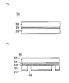
- FIGS. 1 to 4 are views showing a configuration of a wafer substrate bonding structure according to an embodiment.
- a wafer substrate bonding structure 100 may be formed to include a first substrate 110 , a conductive thin film 120 and a second substrate 130 , all of which are sequentially stacked.
- the first substrate 110 may be a conductive substrate.
- the first substrate 110 may be formed of a material such as ZnO, SiO 2 and SnO 2 and the like.
- the conductive thin film 120 may have a form in which a plurality of conductive corpuscles are distributed in a resin.
- the conductive corpuscle may have a diameter of several micrometers.
- the conductive corpuscle may have a shape in which a monodisperse special plastic particle having a diameter of several micrometers is plated with Ni, Au or Cu in the form of a thin film having a thickness of about 100 nm.
- the conductive corpuscle should have a shape in which the monodisperse special plastic particle is plated with an alloy including a material having a low melting point, for example, Au—Sn.
- the resin may include at least one of a thermosetting resin, a thermoplastic resin and a curing agent.
- An epoxy resin may be used as the thermosetting resin.
- An acrylic resin may be used as the thermoplastic resin.
- the conductive thin film may be, for example, an anisotropic conductive film (ACF).
- the second substrate 130 may be stacked on the conductive thin film 120 .
- the second substrate 130 may be either a predetermined substrate (for example, a sapphire substrate and the like) on which a device structure can be formed or a substrate having a thermal expansion coefficient different from that of the first substrate 110 , such as a semiconductor layer which is a portion of the device structure, and the like.
- the first substrate 110 is formed of a material having different properties from those of the material of the second substrate 130 , the first and the second substrates 110 and 130 have mutually different thermal expansion coefficients. As the thermal expansion coefficient difference becomes larger, it becomes more difficult to bond them. For example, it is assumed that the thermal expansion coefficient of the first substrate 110 is greater than that of the second substrate 130 . Then, when a bonding process of the first substrate 110 and the second substrate 130 is performed at a high temperature, the first substrate 110 relatively more expands than the second substrate 130 . Therefore, the first substrate 110 or the second substrate 130 may be damaged.
- the bonding process of the first substrate 110 and the second substrate 130 can be performed at a low temperature. Accordingly, since the bonding process is performed at a low temperature even though the thermal expansion coefficient difference between the first substrate 110 and the second substrate 130 is large, the expansion difference between the first and the second substrates 110 and 130 is insignificant in their bonding and the first and the second substrates 110 and 130 can be securely bonded to each other.
- first and the second substrates 110 and 130 are bonded with the conductive thin film 120 placed therebetween, large-area bonding can be performed and a contact resistance can be hereby considerably reduced. Meanwhile, the resin constituting the conductive thin film 120 may relieve stress between the first substrate 110 and the second substrate 130 .
- a wafer substrate bonding structure 200 may be formed to include a first metal layer 210 , a first substrate 220 , a second metal layer 230 , a conductive thin film 240 and a second substrate 250 , all of which are sequentially stacked.
- the first substrate 220 may be a p-type semiconductor substrate or an n-type semiconductor substrate.
- the conductive thin film 240 and the second substrate 250 are formed of the same materials as those of the conductive thin film 120 and the second substrate 130 respectively. Therefore, detailed descriptions thereof will be omitted.
- the second metal layer 230 helps the first substrate 220 , i.e., a semiconductor substrate to come in ohmic contact with the conductive thin film 240 . That is, the second metal layer 230 minimizes the potential barrier of a carrier of the first substrate 220 , i.e., the semiconductor substrate and reduces the contact resistance between the first substrate 220 and the conductive thin film 240 .
- the first metal layer 210 and the second metal layer 230 may be formed of an alloy including Cr, Ni and Au, Ag, an alloy including Ti and Ag, and the like.
- the first metal layer 210 and the second metal layer 230 may be formed of the same material or may be formed of mutually different materials.
- a wafer substrate bonding structure 300 may include a first substrate 310 , a conductive thin film 320 and a second substrate 330 , all of which are sequentially stacked.
- the first substrate 310 may be a p-type semiconductor substrate or an n-type semiconductor substrate. Since the second substrate 330 is the same as the second substrates 130 and 250 shown in FIGS. 1 and 2 , the description thereof will be omitted.
- Surface metal of the conductive corpuscle included in the conductive thin film 320 according to the third embodiment is formed of a material enabling the first substrate 310 and the conductive thin film 320 to come in ohmic contact with each other. According to this, since the ohmic contact is formed between the first substrate 310 and the conductive thin film 320 , the wafer substrate bonding structure 300 according to the third embodiment does not require the second metal layer 230 of the wafer substrate bonding structure 200 in FIG. 2 , which helps the first substrate 220 to come in ohmic contact with the conductive thin film 240 .
- the first substrate 310 and the conductive thin film 320 are able to come in ohmic contact with each other, but also the first substrate 310 and the second substrate 330 are able to be bonded to each other at a low temperature.
- the surface metal of the conductive corpuscle may be selected in such a relation that when the first substrate 310 is an n-type semiconductor substrate, “fm” ⁇ “fs”, and when the first substrate 310 is a p-type semiconductor substrate, “fm”>“fs”.
- a wafer substrate bonding structure 400 may include a first metal layer 410 , a first substrate 420 , a second metal layer 430 , a conductive thin film 440 , a second substrate 450 and an electrifier 460 , all of which are sequentially stacked.
- the electrifier 460 penetrates the first substrate 420 and electrically connects the first metal layer 410 with the second metal layer 430 .
- the first substrate 420 according to the fourth embodiment may be a nonconductive substrate. Therefore, the electrifier 460 is required in order that the first metal layer 410 and the second metal layer 430 are electrically connected with each other with the first substrate 420 placed therebetween. To this end, the electrifier 460 may be formed of a conductive material. Since other components, i.e., the conductive thin film 440 and the second substrate 450 are the same as those of the first and the second embodiments, the detailed descriptions will be omitted.
- a manufacturing process of the wafer substrate bonding structure 400 according to the fourth embodiment will be described as follows.
- the first metal layer 410 and the first substrate 420 are deposited and at least a portion of the first substrate 420 is removed by an etching process such that the first metal layer 410 is exposed through the removed portion.
- the electrifier 460 is formed by forming a conductive metal in the exposed portion of the first metal layer 410 , and then the second metal layer 430 is formed to cover the first substrate 420 and the electrifier 460 .
- the conductive thin film 440 and the second substrate 450 are formed on the second metal layer 430 . Consequently, the wafer substrate bonding structure 400 according to the fourth embodiment is completed.
- FIGS. 5 a to 5 e are cross sectional views for describing a manufacturing process of a light emitting device by using the wafer substrate bonding structure according to the embodiment. A manufacturing process of a vertical type light emitting device will be described with reference to FIGS. 5 a to 5 e.
- an ohmic layer 520 is formed on the second semiconductor layer 513 .
- the growth substrate 500 may be a sapphire substrate.
- the first semiconductor layer 511 and the active layer 512 may be an N—GaN layer and a P—GaN layer respectively.
- the active layer 512 may be a multi-quantum well (MQW) having a plurality of quantum well structures.
- the ohmic layer 520 may be formed of a material, for example, SiO 2 and the like.
- an insulation layer 530 is formed on the ohmic layer 520 .
- a reflective layer 540 is formed on the insulation layer 530 .
- the insulation layer 530 prevents the semiconductor layers 511 and 513 from being short-circuited due to the reflective layer 540 .
- the reflective layer 540 may be formed of a material such as Ag, Ni or Al and the like.
- the reflective layer 540 may have a central portion thicker than a peripheral portion.
- the wafer substrate bonding structure 200 is formed to cover the reflective layer 540 and the insulation layer 530 .
- the wafer substrate bonding structure 200 may include the first metal layer 210 , the first substrate 220 , the second metal layer 230 and the conductive thin film 240 , all of which are sequentially stacked.
- the wafer substrate bonding structure 200 is formed on the reflective layer 540 in such a manner that the conductive thin film 240 contacts with the reflective layer 540 .
- the drawing shows only the wafer substrate bonding structure 200 of FIG. 2 as a wafer substrate bonding structure included in the light emitting device.
- the wafer substrate bonding structures shown in FIGS. 1 , 3 and 4 may be also used.
- the bonding process can be performed at a low temperature and the stress according to the thermal expansion coefficient difference can be relieved by the resin of the conductive thin film 240 though heat is added.
- a conductive or nonconductive substrate may be further formed on the conductive thin film 240 .
- the conductive or the nonconductive substrate may be further formed between the conductive thin film 240 and the reflective layer 540 .
- a pattern for forming a light emitting structure is formed by an etching process. Then, a protective layer 550 is formed to cover the lateral surface of the light emitting structure.
- the protective layer 550 may be formed of a material, for example, SiO 2 and the like.
- a light extraction structure for example, a texturing structure may be formed on the first semiconductor layer 511 so as to improve light emission efficiency.
- An electrode layer 560 may be also formed on at least a portion of the first semiconductor layer 511 .
- FIGS. 6 a to 6 c are cross sectional views for describing a manufacturing process of the light emitting device by using the wafer substrate bonding structure according to the embodiment. A manufacturing process of a flip-chip type light emitting device will be described with reference to FIGS. 6 a to 6 c.
- a buffer layer 610 , a first semiconductor layer 621 , an active layer 622 and a second semiconductor layer 623 are formed on a growth substrate 600 .
- the buffer layer 610 buffers the lattice mismatch between the growth substrate 600 and an Epi layer and may be formed of a non-doped GaN layer.
- the growth substrate 600 may be a sapphire substrate.
- the first semiconductor layer 621 and the active layer 623 may be an N—GaN layer and a P—GaN layer respectively.
- the active layer 622 may be a multi-quantum well (MQW) having a plurality of quantum well structures.
- MQW multi-quantum well
- a first electrode 630 and a second electrode 640 are formed on the exposed portion of the first semiconductor layer 621 and the second semiconductor layer 623 respectively.
- a reflective layer may be further formed on the second semiconductor layer 623 before the second electrode 640 is formed on the second semiconductor layer 623 .
- the reflective layer is able to not only come in ohmic contact with the second semiconductor layer 623 but also reflect light generated from the active layer 622 toward the first semiconductor layer 621 .
- the flip-chip type light emitting device is completed by bonding the first electrode 630 and the second electrode 640 to the wafer substrate bonding structure 200 .
- a description of a manufacturing process of the wafer substrate bonding structure 200 is the same as the foregoing description and will be omitted. While the drawing shows only the wafer substrate bonding structure 200 of FIG. 2 as a wafer substrate bonding structure, the wafer substrate bonding structures shown in FIGS. 1 , 3 and 4 may be also used. Meanwhile, it is recommended that an insulation layer (not shown) should be formed on the wafer substrate bonding structure 200 for the purpose of insulation between the first electrode 630 and the second electrode 640 .
Landscapes
- Led Devices (AREA)
- Led Device Packages (AREA)
Abstract
Description
Claims (20)
Applications Claiming Priority (2)
| Application Number | Priority Date | Filing Date | Title |
|---|---|---|---|
| KR10-2010-0129173 | 2010-12-16 | ||
| KR1020100129173A KR101189081B1 (en) | 2010-12-16 | 2010-12-16 | Wafer substrate bonding structure, light emitting diode comprising the same and manufacturing method thereof |
Publications (2)
| Publication Number | Publication Date |
|---|---|
| US20120153329A1 US20120153329A1 (en) | 2012-06-21 |
| US8987920B2 true US8987920B2 (en) | 2015-03-24 |
Family
ID=44862775
Family Applications (1)
| Application Number | Title | Priority Date | Filing Date |
|---|---|---|---|
| US13/311,856 Active 2032-03-04 US8987920B2 (en) | 2010-12-16 | 2011-12-06 | Wafer substrate bonding structure and light emitting device comprising the same |
Country Status (4)
| Country | Link |
|---|---|
| US (1) | US8987920B2 (en) |
| EP (1) | EP2466659B1 (en) |
| KR (1) | KR101189081B1 (en) |
| CN (1) | CN102544274B (en) |
Cited By (1)
| Publication number | Priority date | Publication date | Assignee | Title |
|---|---|---|---|---|
| US11114588B2 (en) * | 2017-02-08 | 2021-09-07 | Ushio Denki Kabushiki Kaisha | Semiconductor light emitting element |
Families Citing this family (5)
| Publication number | Priority date | Publication date | Assignee | Title |
|---|---|---|---|---|
| US8624392B2 (en) | 2011-06-03 | 2014-01-07 | Taiwan Semiconductor Manufacturing Company, Ltd. | Electrical connection for chip scale packaging |
| US8912668B2 (en) | 2012-03-01 | 2014-12-16 | Taiwan Semiconductor Manufacturing Company, Ltd. | Electrical connections for chip scale packaging |
| US9196573B2 (en) * | 2012-07-31 | 2015-11-24 | Taiwan Semiconductor Manufacturing Company, Ltd. | Bump on pad (BOP) bonding structure |
| US9673161B2 (en) | 2012-08-17 | 2017-06-06 | Taiwan Semiconductor Manufacturing Company, Ltd. | Bonded structures for package and substrate |
| KR101673259B1 (en) | 2015-02-17 | 2016-11-07 | 엘지전자 주식회사 | Display device using semiconductor light emitting device |
Citations (17)
| Publication number | Priority date | Publication date | Assignee | Title |
|---|---|---|---|---|
| US20050199891A1 (en) | 2004-03-10 | 2005-09-15 | Sanyo Electric Co., Ltd. | Nitride-based semiconductor light-emitting device |
| US20050211989A1 (en) | 2004-03-29 | 2005-09-29 | Stanley Electric Co., Ltd. | Semiconductor light emitting device capable of suppressing silver migration of reflection film made of silver |
| CN1719609A (en) | 2005-07-22 | 2006-01-11 | 金芃 | Metallized silicon chip with antistantic diode |
| JP2007019443A (en) | 2005-07-06 | 2007-01-25 | Creative Technology:Kk | Conductive wafer |
| JP2007035550A (en) | 2005-07-29 | 2007-02-08 | Dainippon Printing Co Ltd | Substrates for electroluminescence elements |
| CN1938904A (en) | 2004-03-30 | 2007-03-28 | 东海橡胶工业株式会社 | Anisotropic conductive film and manufacturing method thereof |
| JP2007087979A (en) | 2005-09-16 | 2007-04-05 | Toshiba Corp | Circuit board and manufacturing method thereof |
| CN101075653A (en) | 2006-09-05 | 2007-11-21 | 武汉迪源光电科技有限公司 | Process for producing quasi-vertical hybrid N-type GaN LED reversed chip with high-doping performance |
| US20080006836A1 (en) * | 2004-10-22 | 2008-01-10 | Seoul Opto-Device Co., Ltd. | GaN Compound Semiconductor Light Emitting Element and Method of Manufacturing the Same |
| US20080048206A1 (en) * | 2006-08-23 | 2008-02-28 | Samsung Electro-Mechanics Co., Ltd. | Vertical gallium nitride-based light emitting diode and method of manufacturing the same |
| US20090008668A1 (en) * | 2007-07-03 | 2009-01-08 | Nichia Corporation | Semiconductor Light Emitting Device and Method for Fabricating the Same |
| CN101523598A (en) | 2006-09-27 | 2009-09-02 | 奥斯兰姆奥普托半导体有限责任公司 | Light-emitting diode arrangement and method for producing the same |
| US20090261370A1 (en) * | 2008-04-21 | 2009-10-22 | Hwan Hee Jeong | Semiconductor light emitting device |
| JP2009253141A (en) | 2008-04-09 | 2009-10-29 | National Institute Of Advanced Industrial & Technology | Electrode for element, manufacturing method therefor, and electronic device equipped with the electrode for element |
| CN101834244A (en) | 2009-03-10 | 2010-09-15 | Lg伊诺特有限公司 | Light emitting device, light emitting device package and lighting system including the same |
| US20100264442A1 (en) * | 2007-12-18 | 2010-10-21 | Seoul Opto Device Co., Ltd. | Light emitting device and method of manufacturing the same |
| US20110233598A1 (en) * | 2010-03-26 | 2011-09-29 | Hon Hai Precision Industry Co., Ltd. | Light emitting diode package and manufacturing method thereof |
Family Cites Families (3)
| Publication number | Priority date | Publication date | Assignee | Title |
|---|---|---|---|---|
| TW277152B (en) * | 1994-05-10 | 1996-06-01 | Hitachi Chemical Co Ltd | |
| KR101166922B1 (en) * | 2005-05-27 | 2012-07-19 | 엘지이노텍 주식회사 | Method of manufacturing light emitting diode |
| KR100720895B1 (en) * | 2005-07-05 | 2007-05-22 | 제일모직주식회사 | Conductive fine particles having a heterogeneous composite metal layer having a concentration gradient, a manufacturing method thereof, and an anisotropic conductive adhesive composition using the same |
-
2010
- 2010-12-16 KR KR1020100129173A patent/KR101189081B1/en not_active Expired - Fee Related
-
2011
- 2011-10-28 EP EP11187163.8A patent/EP2466659B1/en active Active
- 2011-12-01 CN CN201110392382.3A patent/CN102544274B/en not_active Expired - Fee Related
- 2011-12-06 US US13/311,856 patent/US8987920B2/en active Active
Patent Citations (18)
| Publication number | Priority date | Publication date | Assignee | Title |
|---|---|---|---|---|
| US20050199891A1 (en) | 2004-03-10 | 2005-09-15 | Sanyo Electric Co., Ltd. | Nitride-based semiconductor light-emitting device |
| US20050211989A1 (en) | 2004-03-29 | 2005-09-29 | Stanley Electric Co., Ltd. | Semiconductor light emitting device capable of suppressing silver migration of reflection film made of silver |
| CN1938904A (en) | 2004-03-30 | 2007-03-28 | 东海橡胶工业株式会社 | Anisotropic conductive film and manufacturing method thereof |
| US20080006836A1 (en) * | 2004-10-22 | 2008-01-10 | Seoul Opto-Device Co., Ltd. | GaN Compound Semiconductor Light Emitting Element and Method of Manufacturing the Same |
| JP2007019443A (en) | 2005-07-06 | 2007-01-25 | Creative Technology:Kk | Conductive wafer |
| CN1719609A (en) | 2005-07-22 | 2006-01-11 | 金芃 | Metallized silicon chip with antistantic diode |
| JP2007035550A (en) | 2005-07-29 | 2007-02-08 | Dainippon Printing Co Ltd | Substrates for electroluminescence elements |
| JP2007087979A (en) | 2005-09-16 | 2007-04-05 | Toshiba Corp | Circuit board and manufacturing method thereof |
| US20080048206A1 (en) * | 2006-08-23 | 2008-02-28 | Samsung Electro-Mechanics Co., Ltd. | Vertical gallium nitride-based light emitting diode and method of manufacturing the same |
| CN101075653A (en) | 2006-09-05 | 2007-11-21 | 武汉迪源光电科技有限公司 | Process for producing quasi-vertical hybrid N-type GaN LED reversed chip with high-doping performance |
| CN101523598A (en) | 2006-09-27 | 2009-09-02 | 奥斯兰姆奥普托半导体有限责任公司 | Light-emitting diode arrangement and method for producing the same |
| US20100012955A1 (en) | 2006-09-27 | 2010-01-21 | Osram Opto Semiconductors Gmbh | Light-Emitting Diode Arrangement and Method for Producing the Same |
| US20090008668A1 (en) * | 2007-07-03 | 2009-01-08 | Nichia Corporation | Semiconductor Light Emitting Device and Method for Fabricating the Same |
| US20100264442A1 (en) * | 2007-12-18 | 2010-10-21 | Seoul Opto Device Co., Ltd. | Light emitting device and method of manufacturing the same |
| JP2009253141A (en) | 2008-04-09 | 2009-10-29 | National Institute Of Advanced Industrial & Technology | Electrode for element, manufacturing method therefor, and electronic device equipped with the electrode for element |
| US20090261370A1 (en) * | 2008-04-21 | 2009-10-22 | Hwan Hee Jeong | Semiconductor light emitting device |
| CN101834244A (en) | 2009-03-10 | 2010-09-15 | Lg伊诺特有限公司 | Light emitting device, light emitting device package and lighting system including the same |
| US20110233598A1 (en) * | 2010-03-26 | 2011-09-29 | Hon Hai Precision Industry Co., Ltd. | Light emitting diode package and manufacturing method thereof |
Non-Patent Citations (6)
| Title |
|---|
| ASI "Electrically Conductive Adhesives," ASI Adhesives & Sealants, Jul. 1, 2004; retrieved from the Internet: URL: http://www.adhesivesmag.com/articles/print/electrically-conductive-adhesives-1// retrieved Dec. 3, 2013. |
| Chinese Office Action for Application 201110392382.3 dated Jan. 13, 2014. |
| Chinese Office Action issued in related application No. 201110392382.3 dated Jun. 20, 2014. |
| European Search Report for Application 11187163.8 dated Dec. 11, 2013. |
| Korean Notice of Allowance dated Sep. 25, 2012 issued in Application No. 10-2010-0129173. |
| S.M. Sze: "Physics of Semiconductor Devices;" Feb. 2, 2007; Wiley-Interscience, New Jersey, XP055091348 pp. 190-191. |
Cited By (1)
| Publication number | Priority date | Publication date | Assignee | Title |
|---|---|---|---|---|
| US11114588B2 (en) * | 2017-02-08 | 2021-09-07 | Ushio Denki Kabushiki Kaisha | Semiconductor light emitting element |
Also Published As
| Publication number | Publication date |
|---|---|
| CN102544274B (en) | 2015-02-25 |
| EP2466659A2 (en) | 2012-06-20 |
| EP2466659A3 (en) | 2014-01-08 |
| US20120153329A1 (en) | 2012-06-21 |
| KR20120067643A (en) | 2012-06-26 |
| CN102544274A (en) | 2012-07-04 |
| EP2466659B1 (en) | 2020-04-01 |
| KR101189081B1 (en) | 2012-10-10 |
Similar Documents
| Publication | Publication Date | Title |
|---|---|---|
| US8592232B2 (en) | Wafer level LED package and method of fabricating the same | |
| KR101313973B1 (en) | Thin-film led with p and n contacts electrically isolated from the substrate | |
| CN104221173B (en) | Luminous semiconductor device and the method for manufacturing luminous semiconductor device | |
| US9054270B2 (en) | Method for manufacturing light emitting diode chip | |
| US8987920B2 (en) | Wafer substrate bonding structure and light emitting device comprising the same | |
| US9601663B2 (en) | Light-emitting diode chip | |
| US20120326118A1 (en) | Semiconductor light emitting device and method for manufacturing the same | |
| US20130299867A1 (en) | Light-emitting diode chip | |
| US10804424B2 (en) | Method for manufacturing light emitting element | |
| US8759121B2 (en) | Light emitting diode array and method for manufacturing the same | |
| US20140361243A1 (en) | Light emitting device | |
| US20110140137A1 (en) | Led device and method of manufacturing the same | |
| JP2006073618A (en) | Optical element and manufacturing method thereof | |
| JP2014103262A (en) | Method of manufacturing light-emitting device, mounting board, and light-emitting device | |
| TW201225227A (en) | Method for manufacturing heat dissipation bulk of semiconductor device | |
| CN102130241B (en) | Light emitting diode array structure and manufacturing method thereof | |
| KR100953661B1 (en) | Vertical electrode structure light emitting device and manufacturing method thereof | |
| CN101626000B (en) | Metal array substrate, photoelectric element, light emitting element and manufacturing method thereof | |
| CN104979441A (en) | LED chip, manufacturing method thereof, and LED display device with same | |
| CN103474446B (en) | Light emitting diode array structure and manufacturing method thereof | |
| JP2007096090A (en) | Semiconductor light emitting device and method for manufacturing semiconductor light emitting device | |
| US8673667B2 (en) | Method for manufacturing light emitting diode chip | |
| US20060157859A1 (en) | Led packaging method and package structure | |
| KR101482050B1 (en) | Light emitting element array | |
| KR20110038835A (en) | High power light emitting diode and its manufacturing method |
Legal Events
| Date | Code | Title | Description |
|---|---|---|---|
| AS | Assignment |
Owner name: LG INNOTEK CO., LTD., KOREA, REPUBLIC OF Free format text: ASSIGNMENT OF ASSIGNORS INTEREST;ASSIGNOR:CHO, BUM CHUL;REEL/FRAME:027330/0549 Effective date: 20111130 |
|
| FEPP | Fee payment procedure |
Free format text: PAYOR NUMBER ASSIGNED (ORIGINAL EVENT CODE: ASPN); ENTITY STATUS OF PATENT OWNER: LARGE ENTITY |
|
| STCF | Information on status: patent grant |
Free format text: PATENTED CASE |
|
| MAFP | Maintenance fee payment |
Free format text: PAYMENT OF MAINTENANCE FEE, 4TH YEAR, LARGE ENTITY (ORIGINAL EVENT CODE: M1551) Year of fee payment: 4 |
|
| AS | Assignment |
Owner name: SUZHOU LEKIN SEMICONDUCTOR CO., LTD., CHINA Free format text: ASSIGNMENT OF ASSIGNORS INTEREST;ASSIGNOR:LG INNOTEK CO., LTD.;REEL/FRAME:056366/0335 Effective date: 20210520 Owner name: SUZHOU LEKIN SEMICONDUCTOR CO., LTD., CHINA Free format text: ASSIGNMENT OF ASSIGNOR'S INTEREST;ASSIGNOR:LG INNOTEK CO., LTD.;REEL/FRAME:056366/0335 Effective date: 20210520 |
|
| MAFP | Maintenance fee payment |
Free format text: PAYMENT OF MAINTENANCE FEE, 8TH YEAR, LARGE ENTITY (ORIGINAL EVENT CODE: M1552); ENTITY STATUS OF PATENT OWNER: LARGE ENTITY Year of fee payment: 8 |