US8932935B2 - Forming three dimensional isolation structures - Google Patents
Forming three dimensional isolation structures Download PDFInfo
- Publication number
- US8932935B2 US8932935B2 US12/952,240 US95224010A US8932935B2 US 8932935 B2 US8932935 B2 US 8932935B2 US 95224010 A US95224010 A US 95224010A US 8932935 B2 US8932935 B2 US 8932935B2
- Authority
- US
- United States
- Prior art keywords
- trenches
- parallel trenches
- dielectric
- deposition
- depositing
- Prior art date
- Legal status (The legal status is an assumption and is not a legal conclusion. Google has not performed a legal analysis and makes no representation as to the accuracy of the status listed.)
- Active, expires
Links
- 238000002955 isolation Methods 0.000 title abstract description 9
- 238000000151 deposition Methods 0.000 claims abstract description 47
- 230000008021 deposition Effects 0.000 claims abstract description 36
- 238000005229 chemical vapour deposition Methods 0.000 claims abstract description 8
- 230000001590 oxidative effect Effects 0.000 claims abstract description 4
- 238000000034 method Methods 0.000 claims description 27
- 239000000758 substrate Substances 0.000 claims description 10
- 239000004065 semiconductor Substances 0.000 claims description 7
- 238000005530 etching Methods 0.000 claims 4
- 239000003989 dielectric material Substances 0.000 claims 1
- XUIMIQQOPSSXEZ-UHFFFAOYSA-N Silicon Chemical compound [Si] XUIMIQQOPSSXEZ-UHFFFAOYSA-N 0.000 description 8
- 230000003647 oxidation Effects 0.000 description 8
- 238000007254 oxidation reaction Methods 0.000 description 8
- 229910052710 silicon Inorganic materials 0.000 description 8
- 239000010703 silicon Substances 0.000 description 8
- 150000004767 nitrides Chemical class 0.000 description 7
- 239000000945 filler Substances 0.000 description 6
- BOTDANWDWHJENH-UHFFFAOYSA-N Tetraethyl orthosilicate Chemical compound CCO[Si](OCC)(OCC)OCC BOTDANWDWHJENH-UHFFFAOYSA-N 0.000 description 4
- 239000000463 material Substances 0.000 description 3
- 229910052581 Si3N4 Inorganic materials 0.000 description 2
- 230000015572 biosynthetic process Effects 0.000 description 2
- 238000004140 cleaning Methods 0.000 description 2
- 238000011065 in-situ storage Methods 0.000 description 2
- 238000012986 modification Methods 0.000 description 2
- 230000004048 modification Effects 0.000 description 2
- HQVNEWCFYHHQES-UHFFFAOYSA-N silicon nitride Chemical compound N12[Si]34N5[Si]62N3[Si]51N64 HQVNEWCFYHHQES-UHFFFAOYSA-N 0.000 description 2
- 239000011800 void material Substances 0.000 description 2
- CBENFWSGALASAD-UHFFFAOYSA-N Ozone Chemical compound [O-][O+]=O CBENFWSGALASAD-UHFFFAOYSA-N 0.000 description 1
- 230000002411 adverse Effects 0.000 description 1
- 238000000137 annealing Methods 0.000 description 1
- 238000007796 conventional method Methods 0.000 description 1
- 238000005137 deposition process Methods 0.000 description 1
- 238000004519 manufacturing process Methods 0.000 description 1
- 230000000149 penetrating effect Effects 0.000 description 1
- 230000035945 sensitivity Effects 0.000 description 1
- 239000000126 substance Substances 0.000 description 1
- 238000002230 thermal chemical vapour deposition Methods 0.000 description 1
Images


Classifications
-
- H—ELECTRICITY
- H01—ELECTRIC ELEMENTS
- H01L—SEMICONDUCTOR DEVICES NOT COVERED BY CLASS H10
- H01L29/00—Semiconductor devices adapted for rectifying, amplifying, oscillating or switching, or capacitors or resistors with at least one potential-jump barrier or surface barrier, e.g. PN junction depletion layer or carrier concentration layer; Details of semiconductor bodies or of electrodes thereof ; Multistep manufacturing processes therefor
- H01L29/02—Semiconductor bodies ; Multistep manufacturing processes therefor
- H01L29/06—Semiconductor bodies ; Multistep manufacturing processes therefor characterised by their shape; characterised by the shapes, relative sizes, or dispositions of the semiconductor regions ; characterised by the concentration or distribution of impurities within semiconductor regions
- H01L29/0603—Semiconductor bodies ; Multistep manufacturing processes therefor characterised by their shape; characterised by the shapes, relative sizes, or dispositions of the semiconductor regions ; characterised by the concentration or distribution of impurities within semiconductor regions characterised by particular constructional design considerations, e.g. for preventing surface leakage, for controlling electric field concentration or for internal isolations regions
- H01L29/0642—Isolation within the component, i.e. internal isolation
- H01L29/0649—Dielectric regions, e.g. SiO2 regions, air gaps
-
- H—ELECTRICITY
- H01—ELECTRIC ELEMENTS
- H01L—SEMICONDUCTOR DEVICES NOT COVERED BY CLASS H10
- H01L21/00—Processes or apparatus adapted for the manufacture or treatment of semiconductor or solid state devices or of parts thereof
- H01L21/70—Manufacture or treatment of devices consisting of a plurality of solid state components formed in or on a common substrate or of parts thereof; Manufacture of integrated circuit devices or of parts thereof
- H01L21/71—Manufacture of specific parts of devices defined in group H01L21/70
- H01L21/76—Making of isolation regions between components
- H01L21/762—Dielectric regions, e.g. EPIC dielectric isolation, LOCOS; Trench refilling techniques, SOI technology, use of channel stoppers
- H01L21/76224—Dielectric regions, e.g. EPIC dielectric isolation, LOCOS; Trench refilling techniques, SOI technology, use of channel stoppers using trench refilling with dielectric materials
Definitions
- This relates to semiconductor fabrication processes.
- a three dimensional isolation structure is an isolated semiconductor structure with trenches in two perpendicular directions. This structure results in the formation of a regular array of trench isolated pillars. The shape of the pillars is a function of the spacing between the trenches formed in each of the two perpendicular directions.
- a seam is formed in the deposit.
- the seam or void is centrally located in the deposit. This void will then be exposed to subsequent wet etches and cleanings, which can result in damage.
- the conformal film is generally annealed. A wet anneal may be used to close seams and a dry anneal at a higher temperature may be used to decrease the wet etch rate of the film. Thus, the thermal budget may be increased due to the presence of the seams.
- FIG. 1 is a side elevational view at the inception of the process in a second direction
- FIG. 2 is a side elevational view at the same time as FIG. 1 in a first direction perpendicular to said second direction in accordance with one embodiment
- FIG. 3 is a side elevational view in the second direction at a stage subsequent to the stage shown in FIG. 1 ;
- FIG. 4 is a side elevational view in the first direction at the same stage shown in FIG. 3 in accordance with one embodiment
- FIG. 5 is a side elevational view at a stage subsequent to that shown in FIG. 3 in accordance with one embodiment
- FIG. 6 is a side elevational view in the first direction at the same stage shown in FIG. 5 in accordance with one embodiment
- FIG. 7 is a side elevational view at a stage subsequent to that shown in FIG. 5 in accordance with one embodiment
- FIG. 8 is a side elevational view in the first direction of the same stage shown in FIG. 7 ;
- FIG. 9 is a side elevational view at a stage subsequent to that shown in FIG. 7 in accordance with one embodiment
- FIG. 10 is a side elevational view in the first direction at the same stage shown in FIG. 9 in accordance with one embodiment
- FIG. 11 is a side elevational view at a stage subsequent to that shown in FIG. 9 ;
- FIG. 12 is a side elevational view in the first direction of the same stage shown in FIG. 11 in accordance with one embodiment
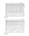
- FIG. 13 is a side elevational view at a stage subsequent to that shown in FIG. 11 in accordance with one embodiment.
- FIG. 14 is a side elevational view in the first direction at the same stage shown in FIG. 13 in accordance with one embodiment.
- a three dimensional isolation structure may be formed in which some of the steps used to form the isolation in one direction are not used in connection with forming the isolation in the other direction.
- a silicon nitride layer 12 may be formed over a silicon substrate 10 in one embodiment.
- a pad oxide 11 may be formed between the layer 12 and the substrate 10 .
- a series of parallel, mostly regularly spaced trenches 14 a may be formed through the nitride layer 12 and partially through the upper portion 10 a of the silicon substrate 10 .
- Active area pillars 13 between trenches may then be made up of nitride over a pad oxide over silicon in some embodiments.
- trench filling is done in the first direction, creating a layer 16 in the second direction, as shown in FIG. 3 , and filling the trenches 14 a in the first direction as shown in FIG. 4 .
- the trench filling may be a combination of a sidewall deposition, followed by conformal film deposition for first direction filling. No anneal or only dry anneal may be used in some embodiments.
- “Sidewall deposition” involves forming a thin liner by oxidizing the substrate.
- Consformal deposition involves depositing, in a trench, a layer that has substantially uniform deposition thickness on the walls and bottom of the trench, as well as on the surface that the trench is formed in. Sidewall deposition may be the same in both the first and second direction trenches of a three dimensional isolation structure, in some embodiments.
- a thick oxide deposition (not shown) may be used to fill the large areas, followed by planarization, as shown in FIGS. 5 and 6 .
- the planarization is done down to the upper surface of the nitride layer 12 in one embodiment.
- the trenches 14 a are filled with the trench filler 16 a.
- the trenches 14 h are formed and filled in the second direction, as shown in FIGS. 7-14 , with the odd numbered figures showing the second direction and the even numbered figures showing the first direction.
- the trenches 14 b in the second direction are deeper than the trenches 14 a in the first direction, as shown in FIG. 7 .
- the trenches 14 b are first treated to encourage ensuing preferential deposition in the trenches 14 b instead of on the existing filler 16 a .
- the treatment may involve covering the surfaces that will preferentially receive the deposition with an appropriate oxidation 22 .
- the oxidation forms preferentially on the silicon nitride layer 12 and the silicon substrate 10 , as shown in FIGS. 7 and 8 .
- the oxidation 22 does not form on the first direction trench filler 16 a ( FIG. 8 ) in one embodiment.
- the ensuing conformal deposition occurs preferentially in the second trenches 14 b .
- the oxidation 22 may be formed by in-situ steam generation (ISSG), which is a steam process that oxidizes active area silicon and nitride, but leaves unchanged the field oxide in the first direction fill. In this manner, a different surface is exposed to the second conformal deposition so that the growth rate is significantly lower than the growth rate where the oxidation is not present.
- ISSG in-situ steam generation
- a sidewall deposition is followed by conformal film deposition, to fill the trenches 14 b , in the second direction, with trench filler 16 b .
- a wet and dry anneal is done, followed by a dry or wet etch back.
- the etch back results in trenches 18 , within the previously filled trenches 14 a and 14 b , in both the second and first directions.
- the trenches 18 may have a wider upper end and a tapered lower end as a result of the nature of the etch back.
- the etch back may occur through the trench fillers 16 a and 16 b between the islands of the nitride layer 12 and partially penetrating within the depth of the silicon substrate 10 .
- the target trench 18 depth may be determined so as to avoid any ensuing wet process on the conformal film, instead relying only on high-density plasma chemical vapor deposition (HDPCVD) in one embodiment.
- HDPCVD high-density plasma chemical vapor deposition
- This etch back may be followed with filling completion by HDPCVD in one embodiment.
- Filling completion involves filling a trench with field oxide completely to its top. Thereafter, final planarization is undertaken, as also shown in FIGS. 13 and 14 to form planarized trench filler 20 .
- TEOS/O 3 tetra-ethyl-ortho-silicate/ozone
- CVD thermal chemical vapor deposition
- recession of those films during the post etch cleaning may be more pronounced due to the higher etch rate after anneal.
- the TEOS/0 3 CVD may use an Applied Materials' (Santa Clara, Calif., USA) sub-atmospheric CVD (SACVD) CXZ chamber or HARP Producer.
- deposition rate may depend on surface composition
- the extent of the differential or selective deposition may be a function of the deposition recipe and thickness. Ideally, a slower deposition rate may be achieved between active pillars and a higher deposition rate may be achieved where there is larger spacing.
- This differential deposition rate may, for example, arise by doing the sidewall deposition by in-situ steam generation (ISSG), which is a steam process which oxidizes the active area silicon and nitride, while leaving the field oxide in the first direction unchanged.
- ISSG in-situ steam generation
- voids may be reduced or eliminated in some embodiments.
- the filling in the second direction may be done using a thin and uniform deposition, avoiding the need for a planarization process before etch back in some embodiments.
- three dimensional isolation structures may be completed using less process steps, and lower total thermal budget, lower active area consumption because of only one wet anneal being performed, less nitride damage and thickness reduction because only one etch back and HDPCVD deposition is used.
- the present invention avoids these problems by doing an oxidation before the second conformal deposition in the second direction. This changes the surface characteristics of the material in the second trench, causing the ensuing conformal dielectric to grow selectively in this area. It does not grow as much (or even at all) in the first direction field oxide already deposited because the oxidation step is ineffective against field oxide.
- the etch back can be done for both directions at the same time and, rather than using a wet etch back, a dry etch back may be used, which creates a slight positive slope of the trenches 18 . This avoids exposing any active area or at least reduces the active area exposure. Active area exposure could result in active area damage or sidewall removal from critical zones, such as the active silicon corner. Because the trenches 18 are relatively shallow, the trench filling using HDPCVD is facilitated. Moreover, the positive slope of the trenches 18 facilitates filling. The HDPCVD deposition done in both directions at the same time also densifies the underlying dielectric still present on the walls to avoid any difference in etch rate of these films.
- references throughout this specification to “one embodiment” or “an embodiment” mean that a particular feature, structure, or characteristic described in connection with the embodiment is included in at least one implementation encompassed within the present invention. Thus, appearances of the phrase “one embodiment” or “in an embodiment” are not necessarily referring to the same embodiment. Furthermore, the particular features, structures, or characteristics may be instituted in other suitable forms other than the particular embodiment illustrated and all such forms may be encompassed within the claims of the present application.
Abstract
Description
Claims (15)
Priority Applications (2)
| Application Number | Priority Date | Filing Date | Title |
|---|---|---|---|
| US12/952,240 US8932935B2 (en) | 2010-11-23 | 2010-11-23 | Forming three dimensional isolation structures |
| US14/567,837 US9111773B2 (en) | 2010-11-23 | 2014-12-11 | Forming three dimensional isolation structures |
Applications Claiming Priority (1)
| Application Number | Priority Date | Filing Date | Title |
|---|---|---|---|
| US12/952,240 US8932935B2 (en) | 2010-11-23 | 2010-11-23 | Forming three dimensional isolation structures |
Related Child Applications (1)
| Application Number | Title | Priority Date | Filing Date |
|---|---|---|---|
| US14/567,837 Division US9111773B2 (en) | 2010-11-23 | 2014-12-11 | Forming three dimensional isolation structures |
Publications (2)
| Publication Number | Publication Date |
|---|---|
| US20120126374A1 US20120126374A1 (en) | 2012-05-24 |
| US8932935B2 true US8932935B2 (en) | 2015-01-13 |
Family
ID=46063569
Family Applications (2)
| Application Number | Title | Priority Date | Filing Date |
|---|---|---|---|
| US12/952,240 Active 2032-06-29 US8932935B2 (en) | 2010-11-23 | 2010-11-23 | Forming three dimensional isolation structures |
| US14/567,837 Active US9111773B2 (en) | 2010-11-23 | 2014-12-11 | Forming three dimensional isolation structures |
Family Applications After (1)
| Application Number | Title | Priority Date | Filing Date |
|---|---|---|---|
| US14/567,837 Active US9111773B2 (en) | 2010-11-23 | 2014-12-11 | Forming three dimensional isolation structures |
Country Status (1)
| Country | Link |
|---|---|
| US (2) | US8932935B2 (en) |
Cited By (1)
| Publication number | Priority date | Publication date | Assignee | Title |
|---|---|---|---|---|
| US20150091128A1 (en) * | 2010-11-23 | 2015-04-02 | Micron Technology, Inc. | Forming three dimensional isolation structures |
Families Citing this family (5)
| Publication number | Priority date | Publication date | Assignee | Title |
|---|---|---|---|---|
| CN103545243B (en) * | 2013-11-13 | 2016-06-29 | 上海华力微电子有限公司 | A kind of forming method of fleet plough groove isolation structure |
| US10269921B2 (en) * | 2014-12-22 | 2019-04-23 | Taiwan Semiconductor Manufacturing Company Ltd. | Fin field effect transistors having conformal oxide layers and methods of forming same |
| US10504821B2 (en) * | 2016-01-29 | 2019-12-10 | United Microelectronics Corp. | Through-silicon via structure |
| CN109119459B (en) * | 2018-08-14 | 2022-03-08 | 上海华虹宏力半导体制造有限公司 | Manufacturing method of groove type super junction |
| CN113707609B (en) * | 2020-05-20 | 2023-07-18 | 长鑫存储技术有限公司 | Method for preparing semiconductor structure |
Citations (3)
| Publication number | Priority date | Publication date | Assignee | Title |
|---|---|---|---|---|
| US20060246684A1 (en) * | 2005-03-25 | 2006-11-02 | Takeshi Hoshi | Method of manufacturing semiconductor device |
| US20080213970A1 (en) * | 2003-05-26 | 2008-09-04 | Stmicroelectronics S.R.L. | Process for the formation of dielectric isolation structures in semiconductor devices |
| US20080305611A1 (en) * | 2007-06-07 | 2008-12-11 | Elpida Memory, Inc. | Coating composition for forming oxide film and method for producing semiconductor device using the same |
Family Cites Families (1)
| Publication number | Priority date | Publication date | Assignee | Title |
|---|---|---|---|---|
| US8932935B2 (en) * | 2010-11-23 | 2015-01-13 | Micron Technology, Inc. | Forming three dimensional isolation structures |
-
2010
- 2010-11-23 US US12/952,240 patent/US8932935B2/en active Active
-
2014
- 2014-12-11 US US14/567,837 patent/US9111773B2/en active Active
Patent Citations (3)
| Publication number | Priority date | Publication date | Assignee | Title |
|---|---|---|---|---|
| US20080213970A1 (en) * | 2003-05-26 | 2008-09-04 | Stmicroelectronics S.R.L. | Process for the formation of dielectric isolation structures in semiconductor devices |
| US20060246684A1 (en) * | 2005-03-25 | 2006-11-02 | Takeshi Hoshi | Method of manufacturing semiconductor device |
| US20080305611A1 (en) * | 2007-06-07 | 2008-12-11 | Elpida Memory, Inc. | Coating composition for forming oxide film and method for producing semiconductor device using the same |
Cited By (2)
| Publication number | Priority date | Publication date | Assignee | Title |
|---|---|---|---|---|
| US20150091128A1 (en) * | 2010-11-23 | 2015-04-02 | Micron Technology, Inc. | Forming three dimensional isolation structures |
| US9111773B2 (en) * | 2010-11-23 | 2015-08-18 | Micron Technology, Inc. | Forming three dimensional isolation structures |
Also Published As
| Publication number | Publication date |
|---|---|
| US9111773B2 (en) | 2015-08-18 |
| US20120126374A1 (en) | 2012-05-24 |
| US20150091128A1 (en) | 2015-04-02 |
Similar Documents
| Publication | Publication Date | Title |
|---|---|---|
| US9111773B2 (en) | Forming three dimensional isolation structures | |
| KR101003494B1 (en) | Isolation structure in memory device and fabricating method for the same | |
| US7915173B2 (en) | Shallow trench isolation structure having reduced dislocation density | |
| US7229896B2 (en) | STI process for eliminating silicon nitride liner induced defects | |
| US20090189246A1 (en) | Method of forming trench isolation structures and semiconductor device produced thereby | |
| US20090017597A1 (en) | Method for manufacturing shallow trench isolation | |
| JP2003197787A (en) | Flash memory cell and method of manufacturing the same | |
| US9093266B2 (en) | Forming high aspect ratio isolation structures | |
| US20070196997A1 (en) | Method of forming isolation structure of semiconductor device | |
| US20090098740A1 (en) | Method of forming isolation layer in semiconductor device | |
| JP2008177277A (en) | Flash memory and method for manufacturing the same | |
| CN107968050B (en) | Method for etching bottom of channel hole | |
| KR20060083249A (en) | Method of forming field oxide in flash memory device | |
| US20090004820A1 (en) | Method of Forming Isolation Layer in Flash Memory Device | |
| KR101060256B1 (en) | Device Separator Formation Method of Semiconductor Device | |
| KR100949867B1 (en) | The method for forming the isolation film of semiconductor device | |
| KR100894792B1 (en) | Method of forming isolation film of semiconductor device | |
| US20050112841A1 (en) | Method for isolating semiconductor devices | |
| KR20120090544A (en) | Semiconductor device and method for manufacturing the same | |
| TW201841353A (en) | Manufacture method of three dimensional flash memory device | |
| KR20110024513A (en) | Method for fabricating semiconductor device | |
| WO2022057338A1 (en) | Manufacturing method for semiconductor structure and semiconductor structure | |
| TW544807B (en) | Method for forming shallow trench isolation | |
| KR20080060318A (en) | Method for forming isolation layer in semiconductor device | |
| KR20070018225A (en) | Method of manufacturing a semiconductor device |
Legal Events
| Date | Code | Title | Description |
|---|---|---|---|
| AS | Assignment |
Owner name: MICRON TECHNOLOGY, INC., IDAHO Free format text: ASSIGNMENT OF ASSIGNORS INTEREST;ASSIGNORS:CAROLLO, ENZO;MARIANI, MARCELLO;MARELLI, SARA;AND OTHERS;REEL/FRAME:025394/0844 Effective date: 20101122 |
|
| AS | Assignment |
Owner name: MICRON TECHNOLOGY, INC., IDAHO Free format text: ASSIGNMENT OF ASSIGNORS INTEREST;ASSIGNOR:NUMONYX B.V.;REEL/FRAME:027126/0176 Effective date: 20110930 |
|
| FEPP | Fee payment procedure |
Free format text: PAYOR NUMBER ASSIGNED (ORIGINAL EVENT CODE: ASPN); ENTITY STATUS OF PATENT OWNER: LARGE ENTITY |
|
| STCF | Information on status: patent grant |
Free format text: PATENTED CASE |
|
| AS | Assignment |
Owner name: U.S. BANK NATIONAL ASSOCIATION, AS COLLATERAL AGENT, CALIFORNIA Free format text: SECURITY INTEREST;ASSIGNOR:MICRON TECHNOLOGY, INC.;REEL/FRAME:038669/0001 Effective date: 20160426 Owner name: U.S. BANK NATIONAL ASSOCIATION, AS COLLATERAL AGEN Free format text: SECURITY INTEREST;ASSIGNOR:MICRON TECHNOLOGY, INC.;REEL/FRAME:038669/0001 Effective date: 20160426 |
|
| AS | Assignment |
Owner name: MORGAN STANLEY SENIOR FUNDING, INC., AS COLLATERAL AGENT, MARYLAND Free format text: PATENT SECURITY AGREEMENT;ASSIGNOR:MICRON TECHNOLOGY, INC.;REEL/FRAME:038954/0001 Effective date: 20160426 Owner name: MORGAN STANLEY SENIOR FUNDING, INC., AS COLLATERAL Free format text: PATENT SECURITY AGREEMENT;ASSIGNOR:MICRON TECHNOLOGY, INC.;REEL/FRAME:038954/0001 Effective date: 20160426 |
|
| AS | Assignment |
Owner name: U.S. BANK NATIONAL ASSOCIATION, AS COLLATERAL AGENT, CALIFORNIA Free format text: CORRECTIVE ASSIGNMENT TO CORRECT THE REPLACE ERRONEOUSLY FILED PATENT #7358718 WITH THE CORRECT PATENT #7358178 PREVIOUSLY RECORDED ON REEL 038669 FRAME 0001. ASSIGNOR(S) HEREBY CONFIRMS THE SECURITY INTEREST;ASSIGNOR:MICRON TECHNOLOGY, INC.;REEL/FRAME:043079/0001 Effective date: 20160426 Owner name: U.S. BANK NATIONAL ASSOCIATION, AS COLLATERAL AGEN Free format text: CORRECTIVE ASSIGNMENT TO CORRECT THE REPLACE ERRONEOUSLY FILED PATENT #7358718 WITH THE CORRECT PATENT #7358178 PREVIOUSLY RECORDED ON REEL 038669 FRAME 0001. ASSIGNOR(S) HEREBY CONFIRMS THE SECURITY INTEREST;ASSIGNOR:MICRON TECHNOLOGY, INC.;REEL/FRAME:043079/0001 Effective date: 20160426 |
|
| MAFP | Maintenance fee payment |
Free format text: PAYMENT OF MAINTENANCE FEE, 4TH YEAR, LARGE ENTITY (ORIGINAL EVENT CODE: M1551) Year of fee payment: 4 |
|
| AS | Assignment |
Owner name: JPMORGAN CHASE BANK, N.A., AS COLLATERAL AGENT, ILLINOIS Free format text: SECURITY INTEREST;ASSIGNORS:MICRON TECHNOLOGY, INC.;MICRON SEMICONDUCTOR PRODUCTS, INC.;REEL/FRAME:047540/0001 Effective date: 20180703 Owner name: JPMORGAN CHASE BANK, N.A., AS COLLATERAL AGENT, IL Free format text: SECURITY INTEREST;ASSIGNORS:MICRON TECHNOLOGY, INC.;MICRON SEMICONDUCTOR PRODUCTS, INC.;REEL/FRAME:047540/0001 Effective date: 20180703 |
|
| AS | Assignment |
Owner name: MICRON TECHNOLOGY, INC., IDAHO Free format text: RELEASE BY SECURED PARTY;ASSIGNOR:U.S. BANK NATIONAL ASSOCIATION, AS COLLATERAL AGENT;REEL/FRAME:047243/0001 Effective date: 20180629 |
|
| AS | Assignment |
Owner name: MICRON TECHNOLOGY, INC., IDAHO Free format text: RELEASE BY SECURED PARTY;ASSIGNOR:MORGAN STANLEY SENIOR FUNDING, INC., AS COLLATERAL AGENT;REEL/FRAME:050937/0001 Effective date: 20190731 |
|
| AS | Assignment |
Owner name: MICRON SEMICONDUCTOR PRODUCTS, INC., IDAHO Free format text: RELEASE BY SECURED PARTY;ASSIGNOR:JPMORGAN CHASE BANK, N.A., AS COLLATERAL AGENT;REEL/FRAME:051028/0001 Effective date: 20190731 Owner name: MICRON TECHNOLOGY, INC., IDAHO Free format text: RELEASE BY SECURED PARTY;ASSIGNOR:JPMORGAN CHASE BANK, N.A., AS COLLATERAL AGENT;REEL/FRAME:051028/0001 Effective date: 20190731 |
|
| MAFP | Maintenance fee payment |
Free format text: PAYMENT OF MAINTENANCE FEE, 8TH YEAR, LARGE ENTITY (ORIGINAL EVENT CODE: M1552); ENTITY STATUS OF PATENT OWNER: LARGE ENTITY Year of fee payment: 8 |