US8922790B2 - Optical film thickness measuring device and thin film forming apparatus using the optical film thickness measuring device - Google Patents

Optical film thickness measuring device and thin film forming apparatus using the optical film thickness measuring device Download PDF

Info

Publication number
US8922790B2
US8922790B2 US13/823,527 US201213823527A US8922790B2 US 8922790 B2 US8922790 B2 US 8922790B2 US 201213823527 A US201213823527 A US 201213823527A US 8922790 B2 US8922790 B2 US 8922790B2
Authority
US
United States
Prior art keywords
film thickness
base substrate
optical
measuring device
measurement
Prior art date
Legal status (The legal status is an assumption and is not a legal conclusion. Google has not performed a legal analysis and makes no representation as to the accuracy of the status listed.)
Active
Application number
US13/823,527
Other versions
US20140016139A1 (en
Inventor
Kyokuyo Sai
Yousong Jiang
Kenji Ozawa
Current Assignee (The listed assignees may be inaccurate. Google has not performed a legal analysis and makes no representation or warranty as to the accuracy of the list.)
Shincron Co Ltd
Original Assignee
Shincron Co Ltd
Priority date (The priority date is an assumption and is not a legal conclusion. Google has not performed a legal analysis and makes no representation as to the accuracy of the date listed.)
Filing date
Publication date
Application filed by Shincron Co Ltd filed Critical Shincron Co Ltd
Assigned to SHINCRON CO., LTD. reassignment SHINCRON CO., LTD. ASSIGNMENT OF ASSIGNORS INTEREST (SEE DOCUMENT FOR DETAILS). Assignors: JIANG, YOUSONG, OZAWA, KENJI, SAI, KYOKUYO
Publication of US20140016139A1 publication Critical patent/US20140016139A1/en
Application granted granted Critical
Publication of US8922790B2 publication Critical patent/US8922790B2/en
Active legal-status Critical Current
Anticipated expiration legal-status Critical

Links

Images

Classifications

    • GPHYSICS
    • G01MEASURING; TESTING
    • G01BMEASURING LENGTH, THICKNESS OR SIMILAR LINEAR DIMENSIONS; MEASURING ANGLES; MEASURING AREAS; MEASURING IRREGULARITIES OF SURFACES OR CONTOURS
    • G01B11/00Measuring arrangements characterised by the use of optical techniques
    • G01B11/02Measuring arrangements characterised by the use of optical techniques for measuring length, width or thickness
    • G01B11/06Measuring arrangements characterised by the use of optical techniques for measuring length, width or thickness for measuring thickness ; e.g. of sheet material
    • G01B11/0691Measuring arrangements characterised by the use of optical techniques for measuring length, width or thickness for measuring thickness ; e.g. of sheet material of objects while moving
    • CCHEMISTRY; METALLURGY
    • C23COATING METALLIC MATERIAL; COATING MATERIAL WITH METALLIC MATERIAL; CHEMICAL SURFACE TREATMENT; DIFFUSION TREATMENT OF METALLIC MATERIAL; COATING BY VACUUM EVAPORATION, BY SPUTTERING, BY ION IMPLANTATION OR BY CHEMICAL VAPOUR DEPOSITION, IN GENERAL; INHIBITING CORROSION OF METALLIC MATERIAL OR INCRUSTATION IN GENERAL
    • C23CCOATING METALLIC MATERIAL; COATING MATERIAL WITH METALLIC MATERIAL; SURFACE TREATMENT OF METALLIC MATERIAL BY DIFFUSION INTO THE SURFACE, BY CHEMICAL CONVERSION OR SUBSTITUTION; COATING BY VACUUM EVAPORATION, BY SPUTTERING, BY ION IMPLANTATION OR BY CHEMICAL VAPOUR DEPOSITION, IN GENERAL
    • C23C14/00Coating by vacuum evaporation, by sputtering or by ion implantation of the coating forming material
    • C23C14/0021Reactive sputtering or evaporation
    • C23C14/0036Reactive sputtering
    • C23C14/0073Reactive sputtering by exposing the substrates to reactive gases intermittently
    • C23C14/0078Reactive sputtering by exposing the substrates to reactive gases intermittently by moving the substrates between spatially separate sputtering and reaction stations
    • CCHEMISTRY; METALLURGY
    • C23COATING METALLIC MATERIAL; COATING MATERIAL WITH METALLIC MATERIAL; CHEMICAL SURFACE TREATMENT; DIFFUSION TREATMENT OF METALLIC MATERIAL; COATING BY VACUUM EVAPORATION, BY SPUTTERING, BY ION IMPLANTATION OR BY CHEMICAL VAPOUR DEPOSITION, IN GENERAL; INHIBITING CORROSION OF METALLIC MATERIAL OR INCRUSTATION IN GENERAL
    • C23CCOATING METALLIC MATERIAL; COATING MATERIAL WITH METALLIC MATERIAL; SURFACE TREATMENT OF METALLIC MATERIAL BY DIFFUSION INTO THE SURFACE, BY CHEMICAL CONVERSION OR SUBSTITUTION; COATING BY VACUUM EVAPORATION, BY SPUTTERING, BY ION IMPLANTATION OR BY CHEMICAL VAPOUR DEPOSITION, IN GENERAL
    • C23C14/00Coating by vacuum evaporation, by sputtering or by ion implantation of the coating forming material
    • C23C14/22Coating by vacuum evaporation, by sputtering or by ion implantation of the coating forming material characterised by the process of coating
    • C23C14/50Substrate holders
    • C23C14/505Substrate holders for rotation of the substrates
    • CCHEMISTRY; METALLURGY
    • C23COATING METALLIC MATERIAL; COATING MATERIAL WITH METALLIC MATERIAL; CHEMICAL SURFACE TREATMENT; DIFFUSION TREATMENT OF METALLIC MATERIAL; COATING BY VACUUM EVAPORATION, BY SPUTTERING, BY ION IMPLANTATION OR BY CHEMICAL VAPOUR DEPOSITION, IN GENERAL; INHIBITING CORROSION OF METALLIC MATERIAL OR INCRUSTATION IN GENERAL
    • C23CCOATING METALLIC MATERIAL; COATING MATERIAL WITH METALLIC MATERIAL; SURFACE TREATMENT OF METALLIC MATERIAL BY DIFFUSION INTO THE SURFACE, BY CHEMICAL CONVERSION OR SUBSTITUTION; COATING BY VACUUM EVAPORATION, BY SPUTTERING, BY ION IMPLANTATION OR BY CHEMICAL VAPOUR DEPOSITION, IN GENERAL
    • C23C14/00Coating by vacuum evaporation, by sputtering or by ion implantation of the coating forming material
    • C23C14/22Coating by vacuum evaporation, by sputtering or by ion implantation of the coating forming material characterised by the process of coating
    • C23C14/54Controlling or regulating the coating process
    • C23C14/542Controlling the film thickness or evaporation rate
    • C23C14/545Controlling the film thickness or evaporation rate using measurement on deposited material
    • C23C14/547Controlling the film thickness or evaporation rate using measurement on deposited material using optical methods
    • GPHYSICS
    • G01MEASURING; TESTING
    • G01BMEASURING LENGTH, THICKNESS OR SIMILAR LINEAR DIMENSIONS; MEASURING ANGLES; MEASURING AREAS; MEASURING IRREGULARITIES OF SURFACES OR CONTOURS
    • G01B11/00Measuring arrangements characterised by the use of optical techniques
    • G01B11/02Measuring arrangements characterised by the use of optical techniques for measuring length, width or thickness
    • G01B11/06Measuring arrangements characterised by the use of optical techniques for measuring length, width or thickness for measuring thickness ; e.g. of sheet material
    • G01B11/0616Measuring arrangements characterised by the use of optical techniques for measuring length, width or thickness for measuring thickness ; e.g. of sheet material of coating
    • G01B11/0625Measuring arrangements characterised by the use of optical techniques for measuring length, width or thickness for measuring thickness ; e.g. of sheet material of coating with measurement of absorption or reflection
    • GPHYSICS
    • G02OPTICS
    • G02BOPTICAL ELEMENTS, SYSTEMS OR APPARATUS
    • G02B26/00Optical devices or arrangements for the control of light using movable or deformable optical elements
    • G02B26/08Optical devices or arrangements for the control of light using movable or deformable optical elements for controlling the direction of light
    • G02B26/10Scanning systems
    • G02B26/12Scanning systems using multifaceted mirrors
    • G02B26/123Multibeam scanners, e.g. using multiple light sources or beam splitters

Definitions

  • the present invention relates to an optical film thickness measuring device and a thin film forming apparatus using the optical film thickness measuring device. More specifically, the present invention relates to an optical film thickness measuring device capable of directly measuring a film thickness of a product and measuring a film distribution, and a thin film forming apparatus using the optical film thickness measuring device.
  • precision optical filters have been generally used in digital cameras, projectors, DVDs, and the like, and a physical vapor deposition (PVD) method such as sputtering or vacuum evaporation has been used in film-formation of these precision optical filters.
  • PVD physical vapor deposition
  • chemical deposition such as CVD has been known as a technique of forming an optical thin film on a surface of a substrate.
  • a carousel-type rotating mechanism is known as an example of a rotating mechanism of a base substrate holding means that holds a substrate (base substrate).
  • a plurality of substrates (base substrates) is held on a peripheral surface of a rotating drum (that is, a base substrate holding means) of which the cross-sectional shape is circular or polygonal, and the rotating drum rotates about a rotating shaft in this state.
  • the substrates (base substrates) since the substrates (base substrates) are held on the peripheral surface of the rotating drum, the substrate (base substrate) may not remain at one position during the rotation of the rotating drum, but all substrates (base substrates) rotate about a rotating shaft.
  • a method of optically measuring a film thickness in real time in a state where the rotating drum rotates may be considered.
  • a method of projecting a measurement beam onto a substrate (base substrate) from the outside of the rotating drum and receiving a reflection beam reflected from the substrate (base substrate) can be considered.
  • the rotating drum since the rotating drum is rotating as described above, there is another problem in that it is difficult to measure the film thickness accurately since the angle of light incident on the substrate (base substrate) changes frequently.
  • the film thickness measuring device includes a rotating drum having a rotating shaft which is a hollow shaft, a total reflection mirror disposed within the rotating shaft, a total reflection mirror disposed on an extension line of the rotating shaft, a light source that emits a measurement beam to the total reflection mirror disposed on the extension line of the rotating shaft via a semi-transparent mirror, and an optical receiver that receives a reflection beam from the total reflection mirror disposed on the extension line of the rotating shaft via the semi-transparent mirror (see, for example, Patent Document 1).
  • the measurement beam from the light source is emitted to the total reflection mirror disposed on the extension line of the rotating shaft via the semi-transparent mirror.
  • the measurement beam emitted to the total reflection mirror within the rotating shaft is reflected to a measurement glass (monitor substrate) held on the rotating drum.
  • the measurement beam emitted to the measurement glass (monitor substrate) is similarly reflected to the total reflection mirror.
  • the reflection beam is emitted to the optical receiver via the semi-transparent mirror.
  • the thin film forming apparatus of the related art since the measurement beam and the reflection beam are guided through the rotating shaft of the rotating drum which is a hollow shaft, it is possible to measure the film thickness of the measurement glass in real time regardless of the fact that the rotating drum is rotating.
  • the film thickness measuring device since the emission of the measurement beam to the measurement glass and the reflection of the reflection beam from the measurement glass (monitor substrate) are realized by the single total reflection mirror provided within the rotating shaft, the measurement beam and the reflection beam are introduced from the same end portion of the rotating shaft. Thus, the intensities of the measurement beam and the reflection beam may change due to wobbling, vibration, or the like of the rotating shaft, and an error may occur in the obtained film thickness value.
  • a film thickness measuring device includes a projecting unit that projects a measurement beam toward an inner portion of a base substrate holding means from one side of an axial line of a rotating shaft, a first optical reflection member that is provided inside the base substrate holding means so as to reflect the measurement beam projected from the projecting unit to a base substrate, a second optical reflection member that is provided inside the base substrate holding means so as to reflect a reflection beam reflected from the base substrate to the other side of the axial line of the rotating shaft, a light receiving unit that receives a reflection beam reflected by the second optical reflection member, and a film thickness computing unit that computes a film thickness of a thin film formed on the base substrate based on the reflection beam received by the light receiving unit (Patent Document 2).
  • Patent Document 1 JP 2000-088531 A (Pages 1 to 5, FIGS. 1 and 2)
  • Patent Document 2 JP 2007-211311 A
  • the technique proposed in Patent Document 2 since the measurement beam and the reflection beam are incident and output from different directions of the axial line of the rotating shaft, it is possible to obtain a high-accuracy film thickness value with small errors.
  • the technique proposed in Patent Document 2 is excellent in that it is possible to obtain a high-accuracy film thickness value with high sensitivity even when measuring the film thickness of a thin film made from a material particularly having low reflectance.
  • the proposed technique when a plurality of substrates is measured, since a monitor substrate is used, a different substrate (at a phase angle of 120°) disposed at a different position is measured. That is, since the position or space where the monitor substrate (monitor glass) is located is different from that of a product substrate (work substrate) that is subjected to film-formation, the measurement is indirect measurement. Thus, since there is a difference between the monitor substrate (monitor glass) and the product substrate (work substrate) that is subjected to film-formation, the thin film is measured by performing correction using predetermined parameters.
  • an optical film thickness meter using a direct-view optical monitor is known.
  • the optical film thickness meter using a direct-view optical monitor is generally designed for a single product substrate (work substrate), and those designed for various product substrates are not known.
  • optical filters having uniform performances can be obtained by repeatedly performing steps of making the film thickness uniform to create a trial film and correcting a correction plate.
  • an object of the present invention is to provide an optical film thickness measuring device capable of directly measuring the film thickness of a product without using a monitor substrate in a thin film forming apparatus that includes a carousel-type rotating mechanism in particular and measuring the film thicknesses of thin films formed on a plurality of substrates disposed in the same line in real time and at a high accuracy.
  • Another object of the present invention is to provide a thin film forming apparatus that uses an optical film thickness measuring device capable of directly measuring a product and controlling the film thickness of the product rather than using a monitor substrate.
  • a further object of the present invention is to provide an optical film thickness measuring device capable of measuring the film thicknesses of products disposed in a plurality of upper and lower stages of a rotating drum using a single optical system and controlling the film thickness, and a thin film forming apparatus using the optical film thickness measuring device.
  • an optical film thickness measuring device for an optical thin film forming apparatus including a rotating base substrate holding means, comprising: a projecting unit that projects a measurement beam from one side of an axial line of a rotating shaft of the rotating base substrate holding means toward the inside of the base substrate holding means, a light receiving unit that receives the measurement beam from the projecting unit, a plurality of inner beam splitters that is provided inside the base substrate holding means so as to reflect the measurement beam projected from the projecting unit to a base substrate, an inner optical reflection member that is provided inside the base substrate holding means so as to totally reflect a measurement beam from the closest inner beam splitter among the plurality of inner beam splitters, a plurality of external beam splitters that is provided outside the base substrate holding means so as to reflect the measurement beam from the plurality of inner beam splitters toward the light receiving unit, and an outer optical reflection member that is provided outside the base substrate holding means so as to reflect the measurement beam from inner the optical reflection member toward the light receiving unit; in
  • the axial line of the rotating shaft of the base substrate holding means prefferably be positioned within a hollow rotating shaft that forms the center of the base substrate holding means, for the inner beam splitter and the inner optical reflection member to be disposed within the rotating shaft, and for the rotating shaft to be configured such that a wall surface of the rotating shaft allows the reflected measurement beam to pass therethrough.
  • the measurement beams reflected by the inner beam splitter and the inner optical reflection member have substantially the same intensity.
  • the optical film thickness measuring device prefferably includes a film thickness computing unit that computes a film thickness of a thin film formed on the base substrate based on the measurement beam received by the light receiving unit.
  • the plurality of external beam splitters and the outer optical reflection member prefferably be covered with a hollow housing, and for a portion of the housing to which the measurement beam is incident to be configured such that the portion allows the measurement beam to pass therethrough.
  • a shutter device prefferably be provided between the plurality of external beam splitters and the outer optical reflection member.
  • the shutter device By using the shutter device in this manner, it is possible to block the optical path, and to exclude a base substrate (substrate) from a measurement target when the base substrate (substrate) as a measurement target is not set.
  • the projecting unit and the light receiving unit are provided in the same direction or at the same planar position of the optical thin film forming apparatus.
  • the projecting unit and the light receiving unit are provided in the same direction of the optical thin film forming apparatus or at the same planar position (for example, on the upper surface of the substrate holding means), since the projecting unit and the light receiving unit are in the same direction or at the same planar position, it is easy to provide the projecting unit and the light receiving unit.
  • the attachment properties and the maintenance properties of the optical film thickness measuring device are improved.
  • the projecting unit and the light receiving unit are positioned on the upper surface, various operations such as attachment or maintenance are made easier than when the projecting unit and the light receiving unit are disposed on the lower surface.
  • the projecting unit and the light receiving unit may be provided in the opposite directions or at the opposite planar positions of the optical thin film forming apparatus.
  • a rotating thin film forming apparatus forming a thin film, using the optical film thickness measuring device according to any one of claims 1 to 8 including: a base substrate holding means capable of rotating about an axial line of a rotating shaft in a state where a base substrate disposed in a vacuum chamber is held, a film raw material supply means that supplies a film raw material for forming the thin film to the vacuum chamber, and a film-formation process area in which the thin film is formed on the base substrate.
  • the thin film forming apparatus of the present invention it is possible to provide an apparatus that uses the properties of the optical film thickness measuring device.
  • the optical film thickness measuring device and the thin film forming apparatus of the present invention since a plurality of beam splitters and total reflection mirrors are arranged along the axial line of the rotating shaft of the base substrate holding means, it is possible to directly measure the film thicknesses of a plurality of base substrates (substrates) to be products which are arranged along the axial line of the rotating shaft of the base substrate holding means. Therefore, by measuring the plurality of base substrates, it is possible to measure the film thicknesses of the base substrates (substrates) which are the actual products and to directly control the film thickness of the product itself rather than a monitor substrate.
  • the present invention it is possible to directly measure the film thickness of a product without using a monitor substrate and to measure the film thicknesses of thin films formed on a plurality of substrates disposed in the same line in real time and at a high accuracy.
  • the optical film thickness measuring device capable of measuring the film thicknesses of the products located at a plurality of upper and lower stages of the rotating drum with the same sensitivity (accuracy) and controlling a film thickness by using one optical system, and a thin film forming apparatus using the optical film thickness measuring device.
  • a movable optical component since a movable optical component is not used, it is possible to obtain high reliability, improve maintenance properties, and to reduce a cost associated with maintenance.
  • FIG. 1 is a cross-sectional explanatory top view of an optical film thickness measuring device and a thin film forming apparatus according to an embodiment of the present invention.
  • FIG. 2 is a cross-sectional explanatory view of the thin film forming apparatus of FIG. 1 along arrows A-A.
  • FIG. 3 is a partial cross-sectional perspective top view of a rotating drum of FIG. 2 .
  • FIG. 4 is a similar partial cross-sectional perspective view to FIG. 3 , illustrating a third embodiment.
  • FIG. 5 is a similar cross-sectional explanatory view to FIG. 2 , illustrating another example of the third embodiment.
  • FIG. 6 is a partial cross-sectional perspective top view of a rotating drum of FIG. 5 .
  • FIG. 7 is a similar cross-sectional explanatory view to FIG. 2 , illustrating another example of a fifth embodiment.
  • FIG. 8 is an explanatory view illustrating an arrangement example of a projection lens.
  • FIG. 9 is an explanatory view of a mirror unit.
  • FIG. 10 is an explanatory view of the mirror unit.
  • FIG. 11 is a block diagram illustrating a functional configuration of an optical film thickness measuring device and a thin film forming apparatus according to each embodiment of the present invention.
  • FIG. 12 is a similar cross-sectional explanatory view to FIG. 2 , illustrating another embodiment.
  • FIG. 13 is an explanatory view of a basic configuration of an optical film thickness measuring device, in which a projecting unit and a light receiving unit are arranged in the same direction.
  • FIG. 14 is an explanatory view of a basic configuration of an optical film thickness measuring device, in which a projecting unit and a light receiving unit are arranged in the opposite directions.
  • FIG. 15 is an explanatory view illustrating methods of calculating optical output in FIGS. 13 and 14 , and comparison of relative optical output.
  • FIG. 16 is a view illustrating the output from a base substrate (substrate) in a first embodiment.
  • FIG. 17 is a view illustrating the output from a base substrate (substrate) in a second embodiment.
  • FIG. 18 is a view illustrating the output from a base substrate (substrate) in a third embodiment.
  • FIG. 19 is a view illustrating the output from a base substrate (substrate) in a fourth embodiment.
  • 35 a , 35 b correction plate driving motor
  • 100 a , 100 b , 100 c optical path switching shutter
  • 165 a to 165 d beam splitter (BS 1 to BS 4 )
  • 166 a to 166 d beam splitter (BS 5 to BS 8 )
  • FIGS. 1 to 19 relates to embodiments of the present invention, in which FIG. 1 is a cross-sectional explanatory top view of an optical film thickness measuring device and a thin film forming apparatus;
  • FIG. 2 is a cross-sectional explanatory view of the thin film forming apparatus of FIG. 1 along arrows A-A;
  • FIG. 3 is a partial cross-sectional perspective top view of a rotating drum of FIG. 2 ;
  • FIG. 4 is a similar partial cross-sectional perspective view to FIG. 3 , illustrating a third embodiment;
  • FIG. 5 is a similar cross-sectional explanatory view to FIG. 2 , illustrating another example of the third embodiment;
  • FIG. 6 is a partial cross-sectional perspective top view of a rotating drum of FIG. 5 ;
  • FIG. 1 is a cross-sectional explanatory top view of an optical film thickness measuring device and a thin film forming apparatus
  • FIG. 2 is a cross-sectional explanatory view of the thin film forming apparatus
  • FIG. 7 is a similar cross-sectional explanatory view to FIG. 2 , illustrating another example of a fifth embodiment
  • FIG. 8 is an explanatory view illustrating an arrangement example of a projection lens
  • FIGS. 9 and 10 are explanatory views of a mirror unit
  • FIG. 11 is a block diagram illustrating a functional configuration of an optical film thickness measuring device and a thin film forming apparatus according to each embodiment
  • FIG. 12 is a similar cross-sectional explanatory view to FIG. 2 , illustrating another embodiment
  • FIG. 13 is an explanatory view of a basic configuration of an optical film thickness measuring device, in which a projecting unit and a light receiving unit are arranged in the same direction;
  • FIG. 14 is an explanatory view of a basic configuration of an optical film thickness measuring device, in which a projecting unit and a light receiving unit are arranged in the opposite directions;
  • FIG. 15 is an explanatory view illustrating methods of calculating optical output in FIGS. 13 and 14 , and comparison of relative optical output;
  • FIG. 16 is a view illustrating the output from a base substrate (substrate) in the first embodiment;
  • FIG. 17 is a view illustrating the output from a base substrate (substrate) in a second embodiment;
  • FIG. 18 is a view illustrating the output from a base substrate (substrate) in a third embodiment;
  • FIG. 19 is a view illustrating the output from a base substrate (substrate) in a fourth embodiment.
  • a thin film forming apparatus 1 of the present embodiment forms an intermediate thin film on a substrate surface by performing a sputtering treatment of sputtering a target to attach a film raw material to a substrate surface so that a thin film comparably thinner than an intended film thickness is attached to the substrate surface and a plasma treatment of performing treatment such as oxidation on the film raw material to transform the composition of the thin film.
  • the thin film forming apparatus 1 stacks a plurality of intermediate thin films by repeating the sputtering treatment and the plasma treatment several times to form a final thin film having an intended film thickness on the substrate surface.
  • an intermediate thin film having an average film thickness of approximately 0.01 nm to 1.5 mm after the composition transform in the sputtering treatment and the plasma treatment is formed on the substrate surface, and a plurality of intermediate thin films is stacked by repeating the treatments every rotation of a rotating drum to form a final thin film having an intended film thickness of approximately several nm to several hundreds of nm.
  • main constituent components of the thin film forming apparatus 1 include a processing chamber 10 that includes a vacuum chamber 11 and a rotating drum 13 , a sputtering means 20 , a sputtering gas supply means 30 , a plasma generation means 40 , a reactive gas supply means 50 , and an optical film thickness measuring device 60 .
  • the sputtering means 20 is surrounded by dashed lines
  • the sputtering gas supply means 30 is surrounded by long dashed short dashed lines
  • the plasma generation means 40 is surrounded by dashed lines
  • the reactive gas supply means 50 is surrounded by long dashed double-short dashed lines.
  • the plasma generation means 40 performs a plasma treatment on the film raw material attached to the surface of a base substrate (substrate) S in a film-formation process treatment to form an intermediate thin film made from a complete reactant or an incomplete reactant of the film raw material.
  • the plasma generation means 40 is configured to include a case member 41 , a dielectric plate 42 , an antenna 43 , a matching box 44 , and a high-frequency power supply 45 .
  • the case member 41 has a shape such that the case member 41 covers an opening formed on a wall surface of the vacuum chamber 11 .
  • the case member 41 is fixed to the wall surface of the vacuum chamber 11 so as to close the opening of the vacuum chamber 11 . In this way, the plasma generation means 40 is attached to the wall surface of the vacuum chamber 11 .
  • Main constituent components of the reactive gas supply means 50 include an oxygen gas cylinder 51 that stores oxygen gas, a mass flow controller 52 that adjusts a flow rate of the oxygen gas supplied from the oxygen gas cylinder 51 , an argon gas cylinder 53 that stores argon gas, a mass flow controller 54 that adjusts a flow rate of the argon gas supplied from the argon gas cylinder 53 , and a pipe 55 that introduces a mixed gas of the oxygen gas and the argon gas to a reaction process area.
  • the plasma generation means 40 performs a plasma treatment on the film raw material attached to the surface of the base substrate (substrate) S by sputtering or the like to form an intermediate thin film made from a complete reactant or an incomplete reactant of the film raw material.
  • the optical film thickness measuring device 60 measures a film thickness of a thin film formed on the surface of the base substrate (substrate) S.
  • the optical film thickness measuring device 60 includes an emission side from which a measurement beam is emitted and a reception side on which the measurement beam having passed through the base substrate (substrate) S is received.
  • FIG. 8 is an explanatory view illustrating an arrangement example of a projection lens on the emission side.
  • the emission side includes a light source 61 that emits a measurement beam, a projection optical fiber 62 that transmits the measurement beam from the light source 61 , and a projection head 63 to which the measurement beam transmitted by the projection optical fiber 62 is guided.
  • the projection head 63 emits the measurement beam to a first beam splitter (BS 1 ) 65 a , a second beam splitter (BS 2 ) 65 b , and a first total reflection mirror 65 c that are disposed within a rotating shaft.
  • a projecting-side focusing lens 64 collects the measurement beam from the projection head 63 .
  • FIGS. 9 and 10 are explanatory views of a mirror unit, in which FIG. 9 is an explanatory view of a mirror unit to which a contamination prevention shield is attached and FIG. 10 is an explanatory view of a mirror unit in which the contamination prevention shield is detached.
  • the total reflection mirror illustrated in FIGS. 9 and 10 is a dielectric mirror.
  • the mirror unit includes the first beam splitter (BS 1 ) 65 a that allows a portion of the measurement beam from the projection head 63 to pass therethrough and guides a portion of the measurement beam to a product base substrate (substrate) S as a base substrate, the second beam splitter (BS 2 ) 65 b that allows another portion of the measurement beam having passed through the first beam splitter (BS 1 ) 65 a to pass therethrough and guides a portion of the measurement beam to the product base substrate (substrate) S, and the first total reflection mirror 65 c that reflects the measurement beam having passed through the second beam splitter (BS 2 ) 65 b .
  • the first beam splitter (BS 1 ) 65 a that allows a portion of the measurement beam from the projection head 63 to pass therethrough and guides a portion of the measurement beam to a product base substrate (substrate) S as a base substrate
  • the second beam splitter (BS 2 ) 65 b that allows another portion of the measurement beam having passed through the first beam splitter (BS
  • the projection optical fiber 62 is connected to the light source 61 , and one end of the projection optical fiber 62 is inserted into the light source 61 so that the measurement beam having passed through a filter of the light source 61 is incident on the end surface of the projection optical fiber 62 and guided to the projection head 63 .
  • the projection head 63 is disposed outside the vacuum chamber 11 on an upper side ( FIG. 2 ) of a rotating shaft 13 a so as to face the first beam splitter (BS 1 ) 65 a , the second beam splitter (BS 2 ) 65 b , and the first total reflection mirror 65 c that are disposed inside the rotating shaft 13 a .
  • the measurement beam emitted from the projection head 63 enters from one end of the rotating shaft 13 a , passes inside the rotating shaft 13 a along the axial direction thereof, and is emitted to the first beam splitter (BS 1 ) 65 a , the second beam splitter (BS 2 ) 65 b , and the first total reflection mirror 65 c.
  • the first beam splitter (BS 1 ) 65 a , the second beam splitter (BS 2 ) 65 b , and the first total reflection mirror 65 c are configured so as to be fixed to a predetermined inner position of the rotating shaft 13 a , and in this case, the angular positions thereof can be adjusted.
  • Main constituent components of the reception side include a third beam splitter (BS 3 ) 66 a , a fourth beam splitter (BS 4 ) 66 b , and a second total reflection mirror 66 c that reflect the measurement beam having passed through the base substrate (substrate) S toward the reception head 69 , a receiving-side focusing lens 68 that collects the measurement beam having passed through or reflected from the third beam splitter (BS 3 ) 66 a , the fourth beam splitter (BS 4 ) 66 b , and the second total reflection mirror 66 c , a reception head 69 , a receiving-side optical fiber 67 that transmits the measurement beam received by the reception head 69 , and a spectroscopic measurement device 71 that disperses the measurement beam transmitted by the receiving-side optical fiber 67 .
  • a third beam splitter (BS 3 ) 66 a a fourth beam splitter (BS 4 ) 66 b , and a second total reflection mirror 66 c
  • the reception side is configured to allow the measurement beam, which has passed through or reflected from the third beam splitter (BS 3 ) 66 a , the fourth beam splitter (BS 4 ) 66 b , and the second total reflection mirror 66 c and has passed through the base substrate (substrate) S, to be reflected from or pass through the third beam splitter (BS 3 ) 66 a , the fourth beam splitter (BS 4 ) 66 b , and the second total reflection mirror 66 c and guide the measurement beam to the spectroscopic measurement device 71 as a measurement beam.
  • the light source 61 , the projection optical fiber 62 , and the projection head 63 correspond to a projecting unit of the present invention.
  • the reception head 69 , the receiving-side optical fiber 67 , and the spectroscopic measurement device 71 correspond to a light receiving unit.
  • the first total reflection mirror 65 c corresponds to an inner optical reflection member
  • the second total reflection mirror 66 c corresponds to an outer optical reflection member.
  • the third beam splitter (BS 3 ) 66 a , the fourth beam splitter (BS 4 ) 66 b , and the second total reflection mirror 66 c on the reception side are configured so as to be fixed to a predetermined position by a holding member (not illustrated) (for example, a rod-shaped member having an optional cross-sectional shape), and in this case, the angular positions thereof can be adjusted.
  • a holding member for example, a rod-shaped member having an optional cross-sectional shape
  • reference numerals 100 a to 100 c designate optical path switching shutters that include a driving unit 101 and shielding plates 102 a to 102 c.
  • the optical path switching shutters 100 a to 100 c have a configuration in which a servo motor (other actuators or the like) is used as the driving unit 101 , the shielding plates 102 a to 102 c are moved by the driving unit 101 , and the shielding plates 102 a to 102 c are moved to a position where the shielding plates 102 a to 102 c block the measurement beam from the emission side so as not to enter the third beam splitter (BS 3 ) 66 a , the fourth beam splitter (BS 4 ) 66 b , and the second total reflection mirror 66 c and a position where the measurement beam is not blocked.
  • a servo motor other actuators or the like
  • the shape or the like of the shielding plates 102 a to 102 c is not particularly limited as long as the shielding plates 102 a to 102 c can block the measurement beam.
  • the driving unit 101 is provided outside the vacuum chamber 11 as a driving source.
  • the shielding plates 102 a to 102 c are configured so as to be moved to a position where the measurement beams from the beam splitters (BS 1 , BS 2 ) 65 a and 65 b and the first total reflection mirror 65 c are not blocked.
  • the shielding plates 102 a to 102 c also have a role of preventing contamination.
  • the driving unit 101 is disposed outside the vacuum chamber.
  • the first total reflection mirror 65 c and the second total reflection mirror 66 c are members prepared by forming a thin film of aluminum or the like on a surface of a base substrate of glass or the like and have high reflectance of approximately 100% at least in the wavelength of the measurement beam.
  • the total reflection mirrors of the present embodiment are formed of a plate-shaped member having an approximately square shape. The total reflection mirrors are arranged inside a hollow body of the rotating shaft 13 a and are fixed to the inner wall surface of the rotating shaft 13 a by welding, screwing, or the like.
  • the light source 61 of the present embodiment uses a halogen lamp, a white LED, or the like and is a device that is provided outside the vacuum chamber 11 so as to emit the measurement beam for measuring a film thickness.
  • the light source 61 includes a light-emitting element 61 a that receives power supplied from a power supply (not illustrated) and emits light and a filter 61 b that allows the light with a specific wavelength region in the light emitted from the light-emitting element 61 a to pass there through.
  • An opening 13 c that is cutout in a portion of a side wall is formed in a central portion of the rotating shaft 13 a , and the measurement beam reflected from the beam splitters (BS 1 , BS 2 ) 65 a and 65 b and the first total reflection mirror 65 c is emitted to the base substrate (substrate) S held on the rotating drum 13 through the opening 13 c .
  • a sealed structure may be created using a glass member through which the light can completely pass.
  • the film thickness of a product substrate itself is directly measured without requiring a monitor substrate for measuring a film thickness.
  • a transparent glass material as the monitor substrate or a plastic or the like as a material that allows the wavelength of the measurement beam to pass therethrough at a high transmittance.
  • the measurement beam emitted from the emission side to the base substrate (substrate) S is divided by the beam splitter into a measurement beam moving toward the base substrate (substrate) S and a passing measurement beam, which are finally reflected by the total reflection mirror.
  • a portion of the measurement beam emitted to the first beam splitter (BS 1 ) 65 a is reflected from the first beam splitter (BS 1 ) 65 a and then enters from a rear surface side (that is, the rotating shaft 13 a side) of the base substrate (substrate) S and passes through the inside of the base substrate (substrate) S.
  • the measurement beam that has passed through the first beam splitter (BS 1 ) 65 a without being reflected is guided to the next second beam splitter (BS 2 ) 65 b , and a portion thereof is reflected from the second beam splitter (BS 2 ) 65 b and then enters from the rear surface side (that is, the rotating shaft 13 a side) of the base substrate (substrate) S and passes through the inside of the base substrate (substrate) S. Further, the measurement beam that has passed through the second beam splitter (BS 2 ) 65 b without being reflected is guided to the first total reflection mirror 65 c .
  • the first total reflection mirror 65 c is formed of a member having high reflectance of approximately 100% in the wavelength of the measurement beam.
  • the reception head 69 is disposed outside the vacuum chamber 11 on the upper side ( FIG. 2 ) of the rotating shaft 13 a , and the third beam splitter (BS 3 ) 66 a , the fourth beam splitter (BS 4 ) 66 b , and the second total reflection mirror 66 c for reflecting the measurement beam emitted from the emission side so as to be guided to the reception head 69 are disposed in a predetermined position on a peripheral side of the rotating drum 13 that is disposed in the vacuum chamber 11 .
  • the reception head 69 is disposed at a position furthest from the sputtering means 20 and the plasma generation means 40 .
  • the reception head 69 is configured to be rarely influenced by the sputtering means 20 and the plasma generation means 40 .
  • the reception head 69 is disposed at a position where the measurement beam reflected by the first beam splitter (BS 1 ) 65 a , the second beam splitter (BS 2 ) 65 b , and the first total reflection mirror 65 c is incident, and one end of the receiving-side optical fiber 67 is connected to the reception head 69 , and the other end is connected to the spectroscopic measurement device 71 .
  • the measurement beam having passed through the base substrate (substrate) S is reflected by the third beam splitter (BS 3 ) 66 a , the fourth beam splitter (BS 4 ) 66 b , and the second total reflection mirror 66 c , collected by the receiving-side focusing lens 68 , and incident on the reception head 69 .
  • the incident measurement beam is guided to the receiving-side optical fiber 67 and input to the spectroscopic measurement device 71 .
  • the projection head 63 and the reception head 69 are provided outside the vacuum chamber 11 , it is possible to prevent problems such as twisting or tangling of an optical fiber due to the rotation of the rotating drum 13 which may occur when the projection head 63 and the reception head 69 are disposed inside the rotating drum 13 .
  • the projection head 63 and the reception head 69 are disposed outside the vacuum chamber 11 , it is possible to eliminate a problem that the rotating drum 13 is heated in the course of film-formation, and the projection head and the reception head are thermally deformed by the heat. In this way, in the present invention, it is possible to prevent the twisting or tangling of the optical fiber and the influence of heat generated in the course of film-formation and to perform stable film thickness measurement.
  • the spectroscopic measurement device 71 is a device that measures the intensity of light of a predetermined wavelength in the reflection beam and has the same configuration as an existing spectroscopic measurement device used in measuring a film thickness. That is, as illustrated in FIG. 11 , the spectroscopic measurement device 71 includes a light-dispersing element 71 b that allows the light within a predetermined wavelength region in the reflection beam to pass therethrough, and a light-receiving element 71 a that receives light having passed through the light-dispersing element 71 b and outputs a current value corresponding to the intensity of the light.
  • the light-dispersing element 71 b is formed of a member having a diffraction lattice such as a grating, for example, and allows the light within a predetermined wavelength region to pass therethrough.
  • the light-dispersing element 71 b allows the wavelength of the measurement beam to pass therethrough at least at the transmittance of approximately 100%.
  • the light having passed through the light-dispersing element 71 b is guided to the light-receiving element 71 a .
  • the light-receiving element 71 a is formed of a semiconductor element such as a photodiode, for example, and an element in which p and n-type semiconductors are bonded may be used, for example.
  • a current corresponding to the intensity of the light is generated.
  • the current is converted into a digital signal by an A/D conversion circuit in the spectroscopic measurement device 71 , and the digital signal is output from the spectroscopic measurement device 71 to a film thickness computing unit 80 described later.
  • the film thickness computing unit 80 is a means that computes the film thickness of a thin film formed on the base substrate (substrate) S based on the intensity of the measurement beam measured by the spectroscopic measurement device 71 .
  • the film thickness computing unit 80 includes a CPU 81 as a computing means, a hard disk 83 and a memory (specifically, ROM and RAM) 82 as a storage means, and an I/O port 84 as an input/output port used when transmitting and receiving signals to/from an external device or the like.
  • the film thickness computing unit 80 corresponds to a film thickness computing unit of the present invention.
  • the film thickness computing unit 80 is electrically connected to the spectroscopic measurement device 71 , and the signal that represents the intensity of the measurement beam and is digitalized by the spectroscopic measurement device 71 is input to the hard disk 83 and the memory (specifically ROM and RAM) 82 as the storage means via the I/O port 84 of the film thickness computing unit 80 .
  • film thickness correlation data 83 a in which a correlation between a change of the intensity of the measurement beam and the film thickness of the thin film formed on the base substrate (substrate) S and a film thickness computation program 83 b that computes a film thickness based on the measurement beam intensity signal transmitted from the spectroscopic measurement device 71 and the film thickness correlation data 83 a are stored in the hard disk 83 .
  • the film thickness correlation data 83 a and the film thickness computation program 83 b may be stored in RAM, ROM, or the like.
  • a measurement beam emitted to the base substrate (substrate) S is reflected at the boundary between the base substrate (substrate) S and the thin film and the boundary between the thin film and the vacuum chamber. In this case, these reflection beams interfere with each other, and the intensity of the reflection beam is changed.
  • a predetermined correlation is present between the intensity of the reflection beam or the transmission beam of the thin film and the film thickness. More specifically, it is known that when a refractive index of a thin film is n, a wavelength is ⁇ , and a geometric film thickness is d, the intensity of a reflection beam exhibits peaks periodically whenever an optical film thickness nd becomes an integer multiple of ⁇ /4. Since the height of peaks (peak value P) and a refractive index have a predetermined correlation, it is possible to obtain a refractive index by obtaining the peak value P. That is, the peak value P is obtained by measuring the intensity of the reflection beam, and the geometric film thickness d can be calculated from the optical film thickness nd based on the values of the refractive index n and the wavelength ⁇ .
  • the film thickness computing unit 80 stores the wavelength ⁇ of the measurement beam as a setting value in advance. Moreover, the film thickness computation program 83 b obtains the height of the peak value P from the reflection beam intensity signal transmitted from the spectroscopic measurement device 71 to compute the refractive index n. Further, the film thickness computation program 83 b calculates the geometric film thickness d based on the values of the refractive index n and the wavelength ⁇ .
  • the film thickness computing unit 80 is electrically connected to the film thickness controller 90 .
  • the film thickness controller 90 includes a computing means such as a MPU, a storage means such as ROM and RAM, and an input/output port that transmits and receives an electrical signal to/from other devices.
  • a film thickness (that is, a geometric film thickness d) measured by the film thickness computing unit 80 is input to the film thickness controller 90 .
  • the film thickness controller 90 includes a film thickness control signal generation unit 91 and controls the film thickness by adjusting a film-formation rate and a film-formation period based on the film thickness signal generated by the film thickness control signal generation unit 91 .
  • the film thickness controller 90 adjusts the film-formation rate based on the film thickness acquired from the film thickness computing unit 80 according to at least one of a method of increasing or decreasing the power supplied to targets 22 a and 22 b from the AC power supply 24 a of the sputtering means 20 , a method of increasing or decreasing the amount of sputtering gas and reactive gas supplied to the film-formation process area by the sputtering gas supply means 30 , and a method of moving the film thickness correction plates 36 a and 36 b by correction plate driving motors 35 a and 35 b .
  • Reference numeral 36 c is a film thickness correction plate, and the film thickness controller 90 corresponds to a film thickness adjustment means.
  • the film thickness may be adjusted by adjusting the film-formation period. That is, when the film thickness of the base substrate (substrate) S acquired by the film thickness computing unit 80 is smaller than a preset film thickness, the film thickness controller 90 extends the film-formation period without ending the film-formation at a predetermined film-formation ending time to increase the film thickness to a preset film thickness. On the other hand, when the film thickness of the base substrate (substrate) S acquired by the film thickness computing unit 80 is larger than a preset film thickness, the film thickness controller 90 shortens the film-formation period by ending the film-formation before a predetermined film-formation ending time to end the film-formation at a preset film thickness.
  • the film thickness may be adjusted by using only one of these film thickness control methods and may be adjusted by a combination of a plurality of methods.
  • the optical film thickness meter can automatically calculate the film-formation rate during the film-formation and control the film thickness. Moreover, by outputting a control signal to an automatic correction plate mechanism, it is possible to control the film thickness and the quality of an optical thin film product. For example, in the case of a stationary photometric method, it is possible to control the film thickness by analyzing the film thickness from the measurement results of the spectroscopic properties of the base substrate (substrate) S.
  • the amount of the transmission beam of the base substrate (substrate) S is measured and the film thickness can be controlled.
  • a basic configuration of the present invention is configured as illustrated in FIGS. 13 to 15 . That is, in the case of one branch, mirrors 1 and 2 are used during projection and reception. In the case of two branches, two BSs (BS 1 , BS 2 ) and two mirrors (mirrors 1 and 2 ) are used during projection and reception. In the case of three branches, four BSs (BS 1 to BS 4 ) and two mirrors (mirrors 1 and 2 ) are used.
  • BSs In the case of four branches, six BSs (BS 1 to BS 6 ) and two mirrors (mirrors 1 and 2 ) are used In the case of five branches, eight BSs (BS 1 to BS 8 ) and two mirrors (mirrors 1 and 2 ) are used.
  • the arrangements of the mirrors and the BSs, when the projecting unit and the light receiving unit are in the same direction and when they are in the opposite directions, are as follows.
  • the mirrors are arranged to face each other when the projecting unit and the light receiving unit are in the same direction, and the mirrors are always arranged so as to face each other at the last reflecting position except for the case of one branch.
  • the receiving-side mirror is fixed to the initially disposed position, and the projecting-side mirror is disposed at a position such that the mirror is moved sequentially downward for every additional branch.
  • FIG. 15 illustrates a table of comparison between the relative outputs for the case of respective branches.
  • the first to fourth embodiments will be described in detail with reference to FIGS. 16 to 19 .
  • the first embodiment is an example in which an aluminum reflection mirror with reflectance of 90% is used as the first and second total reflection mirrors 65 c and 66 c .
  • the first beam splitter (BS 1 ) 65 a has a reflectance/transmittance ratio of 18/82 and the second beam splitter (BS 2 ) 65 b has a reflectance/transmittance ratio of 45/55.
  • the first total reflection mirror 65 c and the second total reflection mirror 66 c are aluminum reflection mirrors and have reflectance of 90%.
  • the third beam splitter (BS 3 ) 66 a and the fourth beam splitter (BS 4 ) 66 b have a reflectance/transmittance ratio of 50/50.
  • the transmittance values (efficiencies) of the measurement beam of the base substrate (substrate) S of the respective products on the upper, middle, and lower stages are 9%, 9.2%, and 9.1%, respectively.
  • the optical path can be switched by the optical path switching shutters 100 a to 100 c.
  • the transmittance values of the base substrate (substrate) S on the upper, middle, and lower stages of the drum are measured in the following order.
  • the transmittance from the base substrate (substrate) S of the upper-stage product to the base substrate (substrate) S of the lower-stage product via the base substrate (substrate) S of the middle-stage product is measured in the following order.
  • optical path switching shutter 100 a is ON ⁇ OFF ⁇ ON
  • optical path switching shutter 100 b is OFF ⁇ ON ⁇ OFF
  • optical path switching shutter 100 c is OFF ⁇ OFF ⁇ OFF.
  • a dark current is measured in the following conditions:
  • Optical path switching shutter 100 a is on, and Optical path switching shutters 100 b and 100 c are off;
  • Optical path switching shutter 100 b is on, and Optical path switching shutters 100 a and 100 c are off;
  • Optical path switching shutter 100 c is on, and Optical path switching shutters 100 a and 100 b are off.
  • the relative light intensities (%) of the upper-stage product base substrate (substrate) S, the middle-stage product base substrate (substrate) S, and the lower-stage product base substrate (substrate) S according to the first embodiment are as illustrated in FIG. 16 .
  • the measurement beam is very evenly distributed.
  • the first beam splitter (BS 1 ) 65 a and the third beam splitter (BS 3 ) 66 a according to the second embodiment are formed of a dielectric mirror and have a reflectance/transmittance ratio of 33.3/66.7 as illustrated in FIG. 17 .
  • the second beam splitter (BS 2 ) 65 b and the fourth beam splitter (BS 4 ) 66 b have a reflectance/transmittance ratio of 50/50.
  • the first total reflection mirror 65 c and the second total reflection mirror 66 c are formed of a dielectric mirror having reflectance of 99.9%. That is, in the first embodiment, an aluminum mirror having reflectance of 90% is used as the first and second total reflection mirrors 65 c and 66 c . In contrast, in the second embodiment, a dielectric mirror having reflectance of 99.9% is used as the first and second total reflection mirrors 65 c and 66 c.
  • the first beam splitter (BS 1 ) 65 a has a reflectance/transmittance ratio of 33.3/66.7
  • the second beam splitter (BS 2 ) 65 b has a reflectance/transmittance ratio of 50/50
  • the dielectric of the first total reflection mirror 65 c and the second total reflection mirror 66 c has reflectance ratio of 99.9%.
  • the third beam splitter (BS 3 ) 66 a has a reflectance/transmittance ratio of 33.3/66.7
  • the fourth beam splitter (BS 4 ) 66 b has a reflectance/transmittance ratio of 50/50.
  • the transmittance values (efficiencies) of the measurement beam of the base substrate (substrate) S of the respective products on the upper, middle, and lower stages are all 11%, 11%, and 11%.
  • the optical path can be switched by the optical path switching shutters 100 a to 100 c.
  • the relative light intensities (%) of the upper-stage product base substrate (substrate) S, the middle-stage product base substrate (substrate) S, and the lower-stage product base substrate (substrate) S according to the second embodiment are as illustrated in FIG. 17 .
  • FIGS. 4 and 18 illustrate the third embodiment, and FIG. 4 illustrates the same partial cross-sectional perspective views as FIG. 3 .
  • the present embodiment illustrates an example in which a shutter device is not used, and five branches are used.
  • the same materials, members, arrangements, and the like as those of the above embodiments will be denoted by the same reference numerals, and description thereof will not be provided.
  • the present embodiment illustrates an example in which four sets of beam splitters ( 165 a to 165 d and 166 a to 166 d ) and one set of total reflection mirrors ( 165 e and 166 e ) are used are used on the emission side and the reception side.
  • the configuration according to this example it is possible to measure the film thicknesses of all base substrates (substrates) S provided on the holding portion.
  • the beam splitter is selected so that the measurement beam to all base substrates (substrates) S has the same intensity. That is, in order to make the intensities of the measurement beams moving toward five base substrates (substrates) S to be the same, a beam splitter configured such that 20% of the measurement beam moves toward the base substrate (substrate) S is used as the first beam splitter (BS 1 ) 165 a . Similarly, a beam splitter configured such that 20%, which is the same amount of beam reflected by the first beam splitter (BS 1 ) 165 a , of the 80% measurement beam having passed through the first beam splitter (BS 1 ) 165 a moves toward the base substrate (substrate) S.
  • the beam splitters are used sequentially. In this way, in the last total reflection mirror 165 e , 20% of the original measurement beam is emitted to the base substrate (substrate) S. Moreover, on the reception side, a beam splitter having a configuration opposite to that of the emission side is used. With the above-described configuration, the optical path switching shutters 100 a to, 100 c are not necessary.
  • the first beam splitter (BS 1 ) 155 a and the fifth beam splitter (BS 5 ) 166 a have a relative light intensity of 20%
  • the second beam splitter (BS 2 ) 165 b and the sixth beam splitter (BS 6 ) 166 b have a relative light intensity of 25%
  • the third beam splitter (BS 3 ) 165 c and the seventh beam splitter (BS 7 ) 166 c have a relative light intensity of 33.3%
  • the fourth beam splitter (BS 4 ) 165 d and the eighth beam splitter (BS 8 ) 166 d have a relative light intensity of 50%.
  • the relative optical output is as follows.
  • Y1:X1 is used for the first beam splitter 1(BS 1 ).
  • FIG. 19 illustrates the fourth embodiment.
  • the first beam splitter (BS 1 ) and the fourth beam splitter (BS 4 ) have a relative light intensity of 75%
  • the second beam splitter (BS 2 ) and the fifth beam splitter (BS 5 ) have a relative light intensity of 33.3%
  • the third beam splitter (BS 3 ) and the sixth beam splitter (BS 6 ) have a relative light intensity of 50%.
  • FIGS. 5 and 6 illustrate another embodiment of the device, in which FIG. 5 is a similar cross-sectional explanatory view to FIG. 2 , and FIG. 6 is a partial cross-sectional perspective top view of the rotating drum of FIG. 5 .
  • FIG. 5 is a similar cross-sectional explanatory view to FIG. 2
  • FIG. 6 is a partial cross-sectional perspective top view of the rotating drum of FIG. 5 .
  • the same materials, members, arrangements, and the like as those of the respective embodiments above will be denoted by the same reference numerals, and description thereof will not be provided.
  • the present embodiment illustrates an example in which the beam splitters 166 a to 166 d and the total reflection mirror 166 e on the reception side are attached within a cylindrical member 160 similarly to the rotating shaft 13 a on the emission side. Moreover, the beam splitters 166 a to 166 d and the total reflection mirror 166 e on the reception side are provided in the cylindrical member 160 by means of an existing means so that the tilt angles thereof can be adjusted. Further, an opening is formed at a position of the cylindrical member 160 corresponding to the optical path of the measurement beam so as not to interrupt the measurement beam moving to the beam splitters 166 a to 166 d and the total reflection mirror 166 e on the reception side. In the present embodiment, although an example in which an opening is formed is illustrated, a sealed structure may be created using a glass member through which light can completely pass.
  • the fifth embodiment illustrated in FIG. 7 will be described.
  • the light receiving unit and the projecting unit are on the opposite sides as illustrated in FIG. 7 .
  • the same materials, members, arrangements, and the like as those of the respective embodiments above will be denoted by the same reference numerals, and description thereof will not be provided.
  • the first beam splitter (BS 1 ) 65 a and the second beam splitter (BS 2 ) 65 b have a reflectance/transmittance ratio of 50%
  • the total reflection mirrors 66 c and 66 k are formed of a dielectric mirror having reflectance of R>99.9%
  • the beam splitter (BS 3 ) 661 and the beam splitter (BS 4 ) 66 m have a reflectance/transmittance ratio of 50%.
  • the device has such a configuration as illustrated in FIGS. 14 and 15 .
  • the projecting unit and the light receiving unit can be configured to be provided in the opposite directions of the optical thin film forming apparatus or on the opposite planar positions.
  • the configurations described in the second to fourth embodiments and illustrated in the respective figures can be applied to this embodiment.
  • FIG. 12 is a similar cross-sectional explanatory view to FIG. 2 , illustrating another embodiment.
  • the beam splitters 65 a and 65 b and the total reflection mirror 65 c on the emission side are disposed inside the rotating shaft 13 a .
  • the rotating shaft 13 a is configured to be maintained as a vacuum by disposing a vacuum magnetic shield for maintaining vacuum.
  • a glass window is disposed on the emission side so as to prevent entrance of foreign materials and impurities. With this configuration, it is not necessary to dispose a contamination prevention shield in the respective beam splitters.

Landscapes

  • Chemical & Material Sciences (AREA)
  • Chemical Kinetics & Catalysis (AREA)
  • Engineering & Computer Science (AREA)
  • Materials Engineering (AREA)
  • Mechanical Engineering (AREA)
  • Metallurgy (AREA)
  • Organic Chemistry (AREA)
  • Physics & Mathematics (AREA)
  • General Physics & Mathematics (AREA)
  • Optics & Photonics (AREA)
  • Length Measuring Devices By Optical Means (AREA)
  • Physical Vapour Deposition (AREA)

Abstract

An optical film thickness measuring device, enabling direct measurement of a film thickness of a product in real time accurately without a monitor substrate, includes: a projector, a light receiver, inner beam splitters disposed in a base substrate holder to reflect a measurement beam to a base substrate, an inner optical reflector that totally reflects a measurement beam from the closest inner beam splitter, external beam splitters the measurement beam from the inner beam splitters toward the light receiver, and an outer optical reflector that reflects the measurement beam from the optical reflector toward the light receiver. The measurement beam reflected by the inner beam splitters and the inner optical reflector is passed through the base substrate and then reflected by the external beam splitters and the outer optical reflector to be guided to the light receiver, so that the measurement beam is received by the light receiver.

Description

TECHNICAL FIELD
The present invention relates to an optical film thickness measuring device and a thin film forming apparatus using the optical film thickness measuring device. More specifically, the present invention relates to an optical film thickness measuring device capable of directly measuring a film thickness of a product and measuring a film distribution, and a thin film forming apparatus using the optical film thickness measuring device.
DESCRIPTION OF THE RELATED ART
In the related art, precision optical filters have been generally used in digital cameras, projectors, DVDs, and the like, and a physical vapor deposition (PVD) method such as sputtering or vacuum evaporation has been used in film-formation of these precision optical filters. Moreover, chemical deposition such as CVD has been known as a technique of forming an optical thin film on a surface of a substrate.
In the field of such a thin film forming technique, a carousel-type rotating mechanism is known as an example of a rotating mechanism of a base substrate holding means that holds a substrate (base substrate). In the carousel-type rotating mechanism, a plurality of substrates (base substrates) is held on a peripheral surface of a rotating drum (that is, a base substrate holding means) of which the cross-sectional shape is circular or polygonal, and the rotating drum rotates about a rotating shaft in this state. In this way, in a carousel-type thin film forming apparatus, since the substrates (base substrates) are held on the peripheral surface of the rotating drum, the substrate (base substrate) may not remain at one position during the rotation of the rotating drum, but all substrates (base substrates) rotate about a rotating shaft.
Therefore, in order to measure optical properties of thin films such as a film thickness according to an optical method, it is necessary to perform optical measurement on a substrate (base substrate) after temporarily stopping the rotation of the rotating drum. In such a measurement method, there is a problem in that the thin film forming step takes a long period of time since the thin film forming step needs to be stopped whenever the film thickness is measured.
In order to solve the above-described problem, a method of optically measuring a film thickness in real time in a state where the rotating drum rotates may be considered. For example, a method of projecting a measurement beam onto a substrate (base substrate) from the outside of the rotating drum and receiving a reflection beam reflected from the substrate (base substrate) can be considered. However, in this method, since the rotating drum is rotating as described above, there is another problem in that it is difficult to measure the film thickness accurately since the angle of light incident on the substrate (base substrate) changes frequently.
In order to solve the respective problems described above, a film thickness measuring device that projects and receives light through a rotating shaft of a rotating drum which is a hollow shaft and a thin film forming apparatus including the film thickness measuring device have been developed. The film thickness measuring device includes a rotating drum having a rotating shaft which is a hollow shaft, a total reflection mirror disposed within the rotating shaft, a total reflection mirror disposed on an extension line of the rotating shaft, a light source that emits a measurement beam to the total reflection mirror disposed on the extension line of the rotating shaft via a semi-transparent mirror, and an optical receiver that receives a reflection beam from the total reflection mirror disposed on the extension line of the rotating shaft via the semi-transparent mirror (see, for example, Patent Document 1).
According to the film thickness measuring device, the measurement beam from the light source is emitted to the total reflection mirror disposed on the extension line of the rotating shaft via the semi-transparent mirror. The measurement beam emitted to the total reflection mirror within the rotating shaft is reflected to a measurement glass (monitor substrate) held on the rotating drum. On the other hand, the measurement beam emitted to the measurement glass (monitor substrate) is similarly reflected to the total reflection mirror. The reflection beam is emitted to the optical receiver via the semi-transparent mirror.
In this way, according to the thin film forming apparatus of the related art, since the measurement beam and the reflection beam are guided through the rotating shaft of the rotating drum which is a hollow shaft, it is possible to measure the film thickness of the measurement glass in real time regardless of the fact that the rotating drum is rotating.
However, in the film thickness measuring device, since the emission of the measurement beam to the measurement glass and the reflection of the reflection beam from the measurement glass (monitor substrate) are realized by the single total reflection mirror provided within the rotating shaft, the measurement beam and the reflection beam are introduced from the same end portion of the rotating shaft. Thus, the intensities of the measurement beam and the reflection beam may change due to wobbling, vibration, or the like of the rotating shaft, and an error may occur in the obtained film thickness value.
Therefore, the present applicant has already proposed a film thickness measurement technique so that the above problem can be solved. According to the proposed technique, a film thickness measuring device includes a projecting unit that projects a measurement beam toward an inner portion of a base substrate holding means from one side of an axial line of a rotating shaft, a first optical reflection member that is provided inside the base substrate holding means so as to reflect the measurement beam projected from the projecting unit to a base substrate, a second optical reflection member that is provided inside the base substrate holding means so as to reflect a reflection beam reflected from the base substrate to the other side of the axial line of the rotating shaft, a light receiving unit that receives a reflection beam reflected by the second optical reflection member, and a film thickness computing unit that computes a film thickness of a thin film formed on the base substrate based on the reflection beam received by the light receiving unit (Patent Document 2).
PRIOR ART DOCUMENTS Patent Documents
Patent Document 1: JP 2000-088531 A (Pages 1 to 5, FIGS. 1 and 2)
Patent Document 2: JP 2007-211311 A
In the technique proposed in Patent Document 2, since the measurement beam and the reflection beam are incident and output from different directions of the axial line of the rotating shaft, it is possible to obtain a high-accuracy film thickness value with small errors. The technique proposed in Patent Document 2 is excellent in that it is possible to obtain a high-accuracy film thickness value with high sensitivity even when measuring the film thickness of a thin film made from a material particularly having low reflectance.
DISCLOSURE OF THE INVENTION Problems to be Solved by the Invention
However, in the proposed technique, when a plurality of substrates is measured, since a monitor substrate is used, a different substrate (at a phase angle of 120°) disposed at a different position is measured. That is, since the position or space where the monitor substrate (monitor glass) is located is different from that of a product substrate (work substrate) that is subjected to film-formation, the measurement is indirect measurement. Thus, since there is a difference between the monitor substrate (monitor glass) and the product substrate (work substrate) that is subjected to film-formation, the thin film is measured by performing correction using predetermined parameters.
In contrast to the indirect measurement, an optical film thickness meter using a direct-view optical monitor is known. However, the optical film thickness meter using a direct-view optical monitor is generally designed for a single product substrate (work substrate), and those designed for various product substrates are not known.
As described above, when a large number of optical filters are produced and manufactured according to PVD or the like, in the case of sputtering and evaporation, for example, a product substrate (work substrate) is disposed on a drum or a dome and a film is formed on the product substrate (work substrate). In this case, optical filters having uniform performances can be obtained by repeatedly performing steps of making the film thickness uniform to create a trial film and correcting a correction plate.
Since a plurality of channels of optical fibers is used to measure a film distribution, an expensive film thickness meter that includes a plurality of spectrometers is required. Thus, there are problems in that an operation of the film thickness meter is complex, and the cost thereof increases.
With the foregoing in view, an object of the present invention is to provide an optical film thickness measuring device capable of directly measuring the film thickness of a product without using a monitor substrate in a thin film forming apparatus that includes a carousel-type rotating mechanism in particular and measuring the film thicknesses of thin films formed on a plurality of substrates disposed in the same line in real time and at a high accuracy.
Another object of the present invention is to provide a thin film forming apparatus that uses an optical film thickness measuring device capable of directly measuring a product and controlling the film thickness of the product rather than using a monitor substrate.
A further object of the present invention is to provide an optical film thickness measuring device capable of measuring the film thicknesses of products disposed in a plurality of upper and lower stages of a rotating drum using a single optical system and controlling the film thickness, and a thin film forming apparatus using the optical film thickness measuring device.
Means for Solving the Problems
According to an optical film thickness measuring device of the present invention, the above objects are solved by an optical film thickness measuring device for an optical thin film forming apparatus including a rotating base substrate holding means, comprising: a projecting unit that projects a measurement beam from one side of an axial line of a rotating shaft of the rotating base substrate holding means toward the inside of the base substrate holding means, a light receiving unit that receives the measurement beam from the projecting unit, a plurality of inner beam splitters that is provided inside the base substrate holding means so as to reflect the measurement beam projected from the projecting unit to a base substrate, an inner optical reflection member that is provided inside the base substrate holding means so as to totally reflect a measurement beam from the closest inner beam splitter among the plurality of inner beam splitters, a plurality of external beam splitters that is provided outside the base substrate holding means so as to reflect the measurement beam from the plurality of inner beam splitters toward the light receiving unit, and an outer optical reflection member that is provided outside the base substrate holding means so as to reflect the measurement beam from inner the optical reflection member toward the light receiving unit; in which the measurement beam reflected by the plurality of inner beam splitters and the inner optical reflection member is passed through the base substrate and then reflected by the plurality of external beam splitters and the outer optical reflection member so as to be guided to the light receiving unit, so that the measurement beam is received by the light receiving unit.
With the configuration, it is possible to directly measure the film thickness of a product without using a monitor substrate and to measure the film thicknesses of thin films formed on a plurality of substrates disposed in the same line in real time and at a high accuracy. Moreover, since a single optical system is used, and a movable optical component is not used, it is possible to have a high reliability and improve maintenance properties.
In this case, it is preferable for the axial line of the rotating shaft of the base substrate holding means to be positioned within a hollow rotating shaft that forms the center of the base substrate holding means, for the inner beam splitter and the inner optical reflection member to be disposed within the rotating shaft, and for the rotating shaft to be configured such that a wall surface of the rotating shaft allows the reflected measurement beam to pass therethrough. In this case, the measurement beams reflected by the inner beam splitter and the inner optical reflection member have substantially the same intensity.
In this way, when measurement beams having the same intensity are emitted to the respective base substrates (substrates) which are products, it is possible to obtain the same measurement sensitivity (accuracy).
Moreover, it is preferable for the optical film thickness measuring device to further include a film thickness computing unit that computes a film thickness of a thin film formed on the base substrate based on the measurement beam received by the light receiving unit.
Further, it is preferable for the plurality of external beam splitters and the outer optical reflection member to be covered with a hollow housing, and for a portion of the housing to which the measurement beam is incident to be configured such that the portion allows the measurement beam to pass therethrough.
With this configuration, it is possible to prevent contamination of the external beam splitter and the outer optical reflection member and to further improve maintenance properties.
Still further, it is preferable for a shutter device to be provided between the plurality of external beam splitters and the outer optical reflection member.
By using the shutter device in this manner, it is possible to block the optical path, and to exclude a base substrate (substrate) from a measurement target when the base substrate (substrate) as a measurement target is not set.
Moreover, it is preferable for the projecting unit and the light receiving unit to be provided in the same direction or at the same planar position of the optical thin film forming apparatus.
As above, when the projecting unit and the light receiving unit are provided in the same direction of the optical thin film forming apparatus or at the same planar position (for example, on the upper surface of the substrate holding means), since the projecting unit and the light receiving unit are in the same direction or at the same planar position, it is easy to provide the projecting unit and the light receiving unit. Thus the attachment properties and the maintenance properties of the optical film thickness measuring device are improved. In particular, since the projecting unit and the light receiving unit are positioned on the upper surface, various operations such as attachment or maintenance are made easier than when the projecting unit and the light receiving unit are disposed on the lower surface.
Moreover, the projecting unit and the light receiving unit may be provided in the opposite directions or at the opposite planar positions of the optical thin film forming apparatus.
By configuring in this way, since the projecting unit and the light receiving unit can be provided on the opposite sides as in the device according to the related art, it is not necessary to change the layout of the device according to the related art.
According to a thin film forming apparatus of the present invention, the above objects are solved by a rotating thin film forming apparatus forming a thin film, using the optical film thickness measuring device according to any one of claims 1 to 8 including: a base substrate holding means capable of rotating about an axial line of a rotating shaft in a state where a base substrate disposed in a vacuum chamber is held, a film raw material supply means that supplies a film raw material for forming the thin film to the vacuum chamber, and a film-formation process area in which the thin film is formed on the base substrate.
According to the thin film forming apparatus of the present invention, it is possible to provide an apparatus that uses the properties of the optical film thickness measuring device.
As described above, according to the optical film thickness measuring device and the thin film forming apparatus of the present invention, since a plurality of beam splitters and total reflection mirrors are arranged along the axial line of the rotating shaft of the base substrate holding means, it is possible to directly measure the film thicknesses of a plurality of base substrates (substrates) to be products which are arranged along the axial line of the rotating shaft of the base substrate holding means. Therefore, by measuring the plurality of base substrates, it is possible to measure the film thicknesses of the base substrates (substrates) which are the actual products and to directly control the film thickness of the product itself rather than a monitor substrate.
Effects of the Invention
According to the present invention, it is possible to directly measure the film thickness of a product without using a monitor substrate and to measure the film thicknesses of thin films formed on a plurality of substrates disposed in the same line in real time and at a high accuracy.
Moreover, fulfilling the performance required for the optical film thickness meter, when a thin film is formed, it is possible to directly measure a base substrate (product substrate) loaded on the rotating base substrate holding means. It is possible to provide an optical film thickness measuring device capable of measuring the film thicknesses of the products located at a plurality of upper and lower stages of the rotating drum with the same sensitivity (accuracy) and controlling a film thickness by using one optical system, and a thin film forming apparatus using the optical film thickness measuring device. In particular, since a movable optical component is not used, it is possible to obtain high reliability, improve maintenance properties, and to reduce a cost associated with maintenance.
BRIEF DESCRIPTION OF DRAWINGS
FIG. 1 is a cross-sectional explanatory top view of an optical film thickness measuring device and a thin film forming apparatus according to an embodiment of the present invention.
FIG. 2 is a cross-sectional explanatory view of the thin film forming apparatus of FIG. 1 along arrows A-A.
FIG. 3 is a partial cross-sectional perspective top view of a rotating drum of FIG. 2.
FIG. 4 is a similar partial cross-sectional perspective view to FIG. 3, illustrating a third embodiment.
FIG. 5 is a similar cross-sectional explanatory view to FIG. 2, illustrating another example of the third embodiment.
FIG. 6 is a partial cross-sectional perspective top view of a rotating drum of FIG. 5.
FIG. 7 is a similar cross-sectional explanatory view to FIG. 2, illustrating another example of a fifth embodiment.
FIG. 8 is an explanatory view illustrating an arrangement example of a projection lens.
FIG. 9 is an explanatory view of a mirror unit.
FIG. 10 is an explanatory view of the mirror unit.
FIG. 11 is a block diagram illustrating a functional configuration of an optical film thickness measuring device and a thin film forming apparatus according to each embodiment of the present invention.
FIG. 12 is a similar cross-sectional explanatory view to FIG. 2, illustrating another embodiment.
FIG. 13 is an explanatory view of a basic configuration of an optical film thickness measuring device, in which a projecting unit and a light receiving unit are arranged in the same direction.
FIG. 14 is an explanatory view of a basic configuration of an optical film thickness measuring device, in which a projecting unit and a light receiving unit are arranged in the opposite directions.
FIG. 15 is an explanatory view illustrating methods of calculating optical output in FIGS. 13 and 14, and comparison of relative optical output.
FIG. 16 is a view illustrating the output from a base substrate (substrate) in a first embodiment.
FIG. 17 is a view illustrating the output from a base substrate (substrate) in a second embodiment.
FIG. 18 is a view illustrating the output from a base substrate (substrate) in a third embodiment.
FIG. 19 is a view illustrating the output from a base substrate (substrate) in a fourth embodiment.
REFERENCE NUMERALS
1: thin film forming apparatus
10: processing chamber
11: vacuum chamber
11 a: thin film forming chamber
11 b: load lock chamber
11 c, 11 d: door
13: rotating drum (base substrate holding means)
13 a: rotating shaft
13 b, 17 a: gear
13 c: opening
14: partition wall
15: vacuum pump
16 a, 16 b: pipe
17: rotating drum driving motor
20: sputtering means
22 a, 22 b: target
24 a: AC power supply
30: sputtering gas supply means
31, 33: mass flow controller
32: sputtering gas cylinder
34: reactive gas cylinder
35: pipe
35 a, 35 b: correction plate driving motor
36 a, 36 b, 36 c: film thickness correction plate
40: plasma generation means
41: case member
42: dielectric plate
43: antenna
44: matching box
45: high-frequency power supply
50: reactive gas supply means
51: oxygen gas cylinder
52, 54: mass flow controller
53: argon gas cylinder
55: pipe
60: optical film thickness measuring device
61: light source
61 a: light-emitting element
61 b: filter
62: projection optical fiber
63: projection head
64: projecting-side focusing lens
65 a: first beam splitter
65 b: second beam splitter
65 c: first total reflection mirror
66 a: third beam splitter
66 b: fourth beam splitter
66 c: second total reflection mirror
66 k: total reflection mirror
66 l, 66 m: beam splitter
67: receiving-side optical fiber
68: receiving-side focusing lens
69: reception head
71: spectroscopic measurement device
71 a: light-receiving element
71 b: light-dispersing element
80: film thickness computing unit
81: CPU
82: memory
83: hard disk
84: I/O port
83 a: film thickness correlation data
83 b: film thickness computation program
90: film thickness controller
91: film thickness control signal generation unit
100 a, 100 b, 100 c: optical path switching shutter
101: driving unit
102 a, 102 b, 102 c: shielding plate
160: cylindrical member
165 a to 165 d: beam splitter (BS1 to BS4)
166 a to 166 d: beam splitter (BS5 to BS8)
165 e, 166 e: total reflection mirror
V: valve
S: base substrate (substrate)
DETAILED DESCRIPTION OF THE INVENTION
Hereinafter, a first embodiment of the present invention will be described with reference to the drawings. Members, arrangements, and the like described below are not limited to the present invention, but may naturally be modified in various manners according to the spirit of the present invention.
FIGS. 1 to 19 relates to embodiments of the present invention, in which FIG. 1 is a cross-sectional explanatory top view of an optical film thickness measuring device and a thin film forming apparatus; FIG. 2 is a cross-sectional explanatory view of the thin film forming apparatus of FIG. 1 along arrows A-A; FIG. 3 is a partial cross-sectional perspective top view of a rotating drum of FIG. 2; FIG. 4 is a similar partial cross-sectional perspective view to FIG. 3, illustrating a third embodiment; FIG. 5 is a similar cross-sectional explanatory view to FIG. 2, illustrating another example of the third embodiment; FIG. 6 is a partial cross-sectional perspective top view of a rotating drum of FIG. 5; FIG. 7 is a similar cross-sectional explanatory view to FIG. 2, illustrating another example of a fifth embodiment; FIG. 8 is an explanatory view illustrating an arrangement example of a projection lens; FIGS. 9 and 10 are explanatory views of a mirror unit; FIG. 11 is a block diagram illustrating a functional configuration of an optical film thickness measuring device and a thin film forming apparatus according to each embodiment; FIG. 12 is a similar cross-sectional explanatory view to FIG. 2, illustrating another embodiment; FIG. 13 is an explanatory view of a basic configuration of an optical film thickness measuring device, in which a projecting unit and a light receiving unit are arranged in the same direction; FIG. 14 is an explanatory view of a basic configuration of an optical film thickness measuring device, in which a projecting unit and a light receiving unit are arranged in the opposite directions; FIG. 15 is an explanatory view illustrating methods of calculating optical output in FIGS. 13 and 14, and comparison of relative optical output; FIG. 16 is a view illustrating the output from a base substrate (substrate) in the first embodiment; FIG. 17 is a view illustrating the output from a base substrate (substrate) in a second embodiment; FIG. 18 is a view illustrating the output from a base substrate (substrate) in a third embodiment; and FIG. 19 is a view illustrating the output from a base substrate (substrate) in a fourth embodiment.
A thin film forming apparatus 1 of the present embodiment forms an intermediate thin film on a substrate surface by performing a sputtering treatment of sputtering a target to attach a film raw material to a substrate surface so that a thin film comparably thinner than an intended film thickness is attached to the substrate surface and a plasma treatment of performing treatment such as oxidation on the film raw material to transform the composition of the thin film. The thin film forming apparatus 1 stacks a plurality of intermediate thin films by repeating the sputtering treatment and the plasma treatment several times to form a final thin film having an intended film thickness on the substrate surface.
Specifically, an intermediate thin film having an average film thickness of approximately 0.01 nm to 1.5 mm after the composition transform in the sputtering treatment and the plasma treatment is formed on the substrate surface, and a plurality of intermediate thin films is stacked by repeating the treatments every rotation of a rotating drum to form a final thin film having an intended film thickness of approximately several nm to several hundreds of nm.
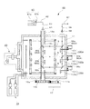
As illustrated in FIGS. 1 and 2, main constituent components of the thin film forming apparatus 1 include a processing chamber 10 that includes a vacuum chamber 11 and a rotating drum 13, a sputtering means 20, a sputtering gas supply means 30, a plasma generation means 40, a reactive gas supply means 50, and an optical film thickness measuring device 60. In the figures, the sputtering means 20 is surrounded by dashed lines, the sputtering gas supply means 30 is surrounded by long dashed short dashed lines, the plasma generation means 40 is surrounded by dashed lines, and the reactive gas supply means 50 is surrounded by long dashed double-short dashed lines.
In a reaction process treatment, the plasma generation means 40 performs a plasma treatment on the film raw material attached to the surface of a base substrate (substrate) S in a film-formation process treatment to form an intermediate thin film made from a complete reactant or an incomplete reactant of the film raw material.
The plasma generation means 40 is configured to include a case member 41, a dielectric plate 42, an antenna 43, a matching box 44, and a high-frequency power supply 45. The case member 41 has a shape such that the case member 41 covers an opening formed on a wall surface of the vacuum chamber 11. The case member 41 is fixed to the wall surface of the vacuum chamber 11 so as to close the opening of the vacuum chamber 11. In this way, the plasma generation means 40 is attached to the wall surface of the vacuum chamber 11.
Main constituent components of the reactive gas supply means 50 include an oxygen gas cylinder 51 that stores oxygen gas, a mass flow controller 52 that adjusts a flow rate of the oxygen gas supplied from the oxygen gas cylinder 51, an argon gas cylinder 53 that stores argon gas, a mass flow controller 54 that adjusts a flow rate of the argon gas supplied from the argon gas cylinder 53, and a pipe 55 that introduces a mixed gas of the oxygen gas and the argon gas to a reaction process area.
Moreover, the plasma generation means 40 performs a plasma treatment on the film raw material attached to the surface of the base substrate (substrate) S by sputtering or the like to form an intermediate thin film made from a complete reactant or an incomplete reactant of the film raw material.
When power is supplied from the high-frequency power supply 45 to the antenna 43 in a state where oxygen gas is introduced into the reaction process area from the oxygen gas cylinder 51 and the argon gas cylinder 53 through an inlet port of the pipe 55, plasma is generated in a region of the reaction process area being facing the antenna 43. By this plasma, silicon (Si) in the film raw material formed on the surface of the base substrate (substrate) S or an incomplete silicon oxide (SiOx (where, 0<x<2)) is oxidized, whereby an intermediate thin film made from a complete silicon oxide (SiO2) or an incomplete silicon oxide (SiOx (where, 0<x<2)) is obtained.
Next, the optical film thickness measuring device 50 according to an embodiment of the present invention will be described. The optical film thickness measuring device 60 measures a film thickness of a thin film formed on the surface of the base substrate (substrate) S. In the present embodiment, as illustrated in FIGS. 2 to 7 and 12, the optical film thickness measuring device 60 includes an emission side from which a measurement beam is emitted and a reception side on which the measurement beam having passed through the base substrate (substrate) S is received.
FIG. 8 is an explanatory view illustrating an arrangement example of a projection lens on the emission side. The emission side includes a light source 61 that emits a measurement beam, a projection optical fiber 62 that transmits the measurement beam from the light source 61, and a projection head 63 to which the measurement beam transmitted by the projection optical fiber 62 is guided.
The projection head 63 emits the measurement beam to a first beam splitter (BS1) 65 a, a second beam splitter (BS2) 65 b, and a first total reflection mirror 65 c that are disposed within a rotating shaft. A projecting-side focusing lens 64 collects the measurement beam from the projection head 63.
FIGS. 9 and 10 are explanatory views of a mirror unit, in which FIG. 9 is an explanatory view of a mirror unit to which a contamination prevention shield is attached and FIG. 10 is an explanatory view of a mirror unit in which the contamination prevention shield is detached. The total reflection mirror illustrated in FIGS. 9 and 10 is a dielectric mirror.
In the present embodiment, the mirror unit includes the first beam splitter (BS1) 65 a that allows a portion of the measurement beam from the projection head 63 to pass therethrough and guides a portion of the measurement beam to a product base substrate (substrate) S as a base substrate, the second beam splitter (BS2) 65 b that allows another portion of the measurement beam having passed through the first beam splitter (BS1) 65 a to pass therethrough and guides a portion of the measurement beam to the product base substrate (substrate) S, and the first total reflection mirror 65 c that reflects the measurement beam having passed through the second beam splitter (BS2) 65 b. The projection optical fiber 62 is connected to the light source 61, and one end of the projection optical fiber 62 is inserted into the light source 61 so that the measurement beam having passed through a filter of the light source 61 is incident on the end surface of the projection optical fiber 62 and guided to the projection head 63.
The projection head 63 is disposed outside the vacuum chamber 11 on an upper side (FIG. 2) of a rotating shaft 13 a so as to face the first beam splitter (BS1) 65 a, the second beam splitter (BS2) 65 b, and the first total reflection mirror 65 c that are disposed inside the rotating shaft 13 a. The measurement beam emitted from the projection head 63 enters from one end of the rotating shaft 13 a, passes inside the rotating shaft 13 a along the axial direction thereof, and is emitted to the first beam splitter (BS1) 65 a, the second beam splitter (BS2) 65 b, and the first total reflection mirror 65 c.
The first beam splitter (BS1) 65 a, the second beam splitter (BS2) 65 b, and the first total reflection mirror 65 c are configured so as to be fixed to a predetermined inner position of the rotating shaft 13 a, and in this case, the angular positions thereof can be adjusted.
Main constituent components of the reception side include a third beam splitter (BS3) 66 a, a fourth beam splitter (BS4) 66 b, and a second total reflection mirror 66 c that reflect the measurement beam having passed through the base substrate (substrate) S toward the reception head 69, a receiving-side focusing lens 68 that collects the measurement beam having passed through or reflected from the third beam splitter (BS3) 66 a, the fourth beam splitter (BS4) 66 b, and the second total reflection mirror 66 c, a reception head 69, a receiving-side optical fiber 67 that transmits the measurement beam received by the reception head 69, and a spectroscopic measurement device 71 that disperses the measurement beam transmitted by the receiving-side optical fiber 67. That is, the reception side is configured to allow the measurement beam, which has passed through or reflected from the third beam splitter (BS3) 66 a, the fourth beam splitter (BS4) 66 b, and the second total reflection mirror 66 c and has passed through the base substrate (substrate) S, to be reflected from or pass through the third beam splitter (BS3) 66 a, the fourth beam splitter (BS4) 66 b, and the second total reflection mirror 66 c and guide the measurement beam to the spectroscopic measurement device 71 as a measurement beam.
Further, the light source 61, the projection optical fiber 62, and the projection head 63 correspond to a projecting unit of the present invention. Further, the reception head 69, the receiving-side optical fiber 67, and the spectroscopic measurement device 71 correspond to a light receiving unit. Moreover, the first total reflection mirror 65 c corresponds to an inner optical reflection member, and the second total reflection mirror 66 c corresponds to an outer optical reflection member.
The third beam splitter (BS3) 66 a, the fourth beam splitter (BS4) 66 b, and the second total reflection mirror 66 c on the reception side are configured so as to be fixed to a predetermined position by a holding member (not illustrated) (for example, a rod-shaped member having an optional cross-sectional shape), and in this case, the angular positions thereof can be adjusted.
Moreover, reference numerals 100 a to 100 c designate optical path switching shutters that include a driving unit 101 and shielding plates 102 a to 102 c.
The optical path switching shutters 100 a to 100 c have a configuration in which a servo motor (other actuators or the like) is used as the driving unit 101, the shielding plates 102 a to 102 c are moved by the driving unit 101, and the shielding plates 102 a to 102 c are moved to a position where the shielding plates 102 a to 102 c block the measurement beam from the emission side so as not to enter the third beam splitter (BS3) 66 a, the fourth beam splitter (BS4) 66 b, and the second total reflection mirror 66 c and a position where the measurement beam is not blocked. The shape or the like of the shielding plates 102 a to 102 c is not particularly limited as long as the shielding plates 102 a to 102 c can block the measurement beam. In the optical path switching shutters 100 a to 100 c, the driving unit 101 is provided outside the vacuum chamber 11 as a driving source.
The shielding plates 102 a to 102 c are configured so as to be moved to a position where the measurement beams from the beam splitters (BS1, BS2) 65 a and 65 b and the first total reflection mirror 65 c are not blocked. The shielding plates 102 a to 102 c also have a role of preventing contamination. The driving unit 101 is disposed outside the vacuum chamber.
Moreover, the first total reflection mirror 65 c and the second total reflection mirror 66 c are members prepared by forming a thin film of aluminum or the like on a surface of a base substrate of glass or the like and have high reflectance of approximately 100% at least in the wavelength of the measurement beam. The total reflection mirrors of the present embodiment are formed of a plate-shaped member having an approximately square shape. The total reflection mirrors are arranged inside a hollow body of the rotating shaft 13 a and are fixed to the inner wall surface of the rotating shaft 13 a by welding, screwing, or the like.
The light source 61 of the present embodiment uses a halogen lamp, a white LED, or the like and is a device that is provided outside the vacuum chamber 11 so as to emit the measurement beam for measuring a film thickness. As illustrated in FIG. 11, the light source 61 includes a light-emitting element 61 a that receives power supplied from a power supply (not illustrated) and emits light and a filter 61 b that allows the light with a specific wavelength region in the light emitted from the light-emitting element 61 a to pass there through.
An opening 13 c that is cutout in a portion of a side wall is formed in a central portion of the rotating shaft 13 a, and the measurement beam reflected from the beam splitters (BS1, BS2) 65 a and 65 b and the first total reflection mirror 65 c is emitted to the base substrate (substrate) S held on the rotating drum 13 through the opening 13 c. Moreover, in the present embodiment, although an example in which the opening 13 c is formed is illustrated, a sealed structure may be created using a glass member through which the light can completely pass.
As described above, in the present invention, unlike the related art, the film thickness of a product substrate itself is directly measured without requiring a monitor substrate for measuring a film thickness. Moreover, unlike the related art, it is not necessary to use a transparent glass material as the monitor substrate or a plastic or the like as a material that allows the wavelength of the measurement beam to pass therethrough at a high transmittance.
The measurement beam emitted from the emission side to the base substrate (substrate) S is divided by the beam splitter into a measurement beam moving toward the base substrate (substrate) S and a passing measurement beam, which are finally reflected by the total reflection mirror.
That is, a portion of the measurement beam emitted to the first beam splitter (BS1) 65 a is reflected from the first beam splitter (BS1) 65 a and then enters from a rear surface side (that is, the rotating shaft 13 a side) of the base substrate (substrate) S and passes through the inside of the base substrate (substrate) S. The measurement beam that has passed through the first beam splitter (BS1) 65 a without being reflected is guided to the next second beam splitter (BS2) 65 b, and a portion thereof is reflected from the second beam splitter (BS2) 65 b and then enters from the rear surface side (that is, the rotating shaft 13 a side) of the base substrate (substrate) S and passes through the inside of the base substrate (substrate) S. Further, the measurement beam that has passed through the second beam splitter (BS2) 65 b without being reflected is guided to the first total reflection mirror 65 c. The first total reflection mirror 65 c is formed of a member having high reflectance of approximately 100% in the wavelength of the measurement beam. These measurement beams emitted from the emission side are received on the reception side.
Similarly to the projection head 63, the reception head 69 is disposed outside the vacuum chamber 11 on the upper side (FIG. 2) of the rotating shaft 13 a, and the third beam splitter (BS3) 66 a, the fourth beam splitter (BS4) 66 b, and the second total reflection mirror 66 c for reflecting the measurement beam emitted from the emission side so as to be guided to the reception head 69 are disposed in a predetermined position on a peripheral side of the rotating drum 13 that is disposed in the vacuum chamber 11. In the present embodiment, as illustrated in FIG. 2, the reception head 69 is disposed at a position furthest from the sputtering means 20 and the plasma generation means 40. As a result, the reception head 69 is configured to be rarely influenced by the sputtering means 20 and the plasma generation means 40.
The reception head 69 is disposed at a position where the measurement beam reflected by the first beam splitter (BS1) 65 a, the second beam splitter (BS2) 65 b, and the first total reflection mirror 65 c is incident, and one end of the receiving-side optical fiber 67 is connected to the reception head 69, and the other end is connected to the spectroscopic measurement device 71. The measurement beam having passed through the base substrate (substrate) S is reflected by the third beam splitter (BS3) 66 a, the fourth beam splitter (BS4) 66 b, and the second total reflection mirror 66 c, collected by the receiving-side focusing lens 68, and incident on the reception head 69. The incident measurement beam is guided to the receiving-side optical fiber 67 and input to the spectroscopic measurement device 71.
As described above, since the projection head 63 and the reception head 69 are provided outside the vacuum chamber 11, it is possible to prevent problems such as twisting or tangling of an optical fiber due to the rotation of the rotating drum 13 which may occur when the projection head 63 and the reception head 69 are disposed inside the rotating drum 13. Moreover, the projection head 63 and the reception head 69 are disposed outside the vacuum chamber 11, it is possible to eliminate a problem that the rotating drum 13 is heated in the course of film-formation, and the projection head and the reception head are thermally deformed by the heat. In this way, in the present invention, it is possible to prevent the twisting or tangling of the optical fiber and the influence of heat generated in the course of film-formation and to perform stable film thickness measurement.
The spectroscopic measurement device 71 is a device that measures the intensity of light of a predetermined wavelength in the reflection beam and has the same configuration as an existing spectroscopic measurement device used in measuring a film thickness. That is, as illustrated in FIG. 11, the spectroscopic measurement device 71 includes a light-dispersing element 71 b that allows the light within a predetermined wavelength region in the reflection beam to pass therethrough, and a light-receiving element 71 a that receives light having passed through the light-dispersing element 71 b and outputs a current value corresponding to the intensity of the light.
The light-dispersing element 71 b is formed of a member having a diffraction lattice such as a grating, for example, and allows the light within a predetermined wavelength region to pass therethrough. In the present embodiment, the light-dispersing element 71 b allows the wavelength of the measurement beam to pass therethrough at least at the transmittance of approximately 100%. The light having passed through the light-dispersing element 71 b is guided to the light-receiving element 71 a. The light-receiving element 71 a is formed of a semiconductor element such as a photodiode, for example, and an element in which p and n-type semiconductors are bonded may be used, for example. When light strikes the bonding surface of the p and n-type semiconductors, a current corresponding to the intensity of the light is generated. The current is converted into a digital signal by an A/D conversion circuit in the spectroscopic measurement device 71, and the digital signal is output from the spectroscopic measurement device 71 to a film thickness computing unit 80 described later.
The film thickness computing unit 80 is a means that computes the film thickness of a thin film formed on the base substrate (substrate) S based on the intensity of the measurement beam measured by the spectroscopic measurement device 71. As illustrated in FIG. 11, the film thickness computing unit 80 includes a CPU 81 as a computing means, a hard disk 83 and a memory (specifically, ROM and RAM) 82 as a storage means, and an I/O port 84 as an input/output port used when transmitting and receiving signals to/from an external device or the like. The film thickness computing unit 80 corresponds to a film thickness computing unit of the present invention.
The film thickness computing unit 80 is electrically connected to the spectroscopic measurement device 71, and the signal that represents the intensity of the measurement beam and is digitalized by the spectroscopic measurement device 71 is input to the hard disk 83 and the memory (specifically ROM and RAM) 82 as the storage means via the I/O port 84 of the film thickness computing unit 80. For example, film thickness correlation data 83 a in which a correlation between a change of the intensity of the measurement beam and the film thickness of the thin film formed on the base substrate (substrate) S and a film thickness computation program 83 b that computes a film thickness based on the measurement beam intensity signal transmitted from the spectroscopic measurement device 71 and the film thickness correlation data 83 a are stored in the hard disk 83. The film thickness correlation data 83 a and the film thickness computation program 83 b may be stored in RAM, ROM, or the like.
Hereinafter, a principle of measuring the film thickness using the film thickness computing unit 80 will be described. A measurement beam emitted to the base substrate (substrate) S is reflected at the boundary between the base substrate (substrate) S and the thin film and the boundary between the thin film and the vacuum chamber. In this case, these reflection beams interfere with each other, and the intensity of the reflection beam is changed.
Here, a predetermined correlation is present between the intensity of the reflection beam or the transmission beam of the thin film and the film thickness. More specifically, it is known that when a refractive index of a thin film is n, a wavelength is λ, and a geometric film thickness is d, the intensity of a reflection beam exhibits peaks periodically whenever an optical film thickness nd becomes an integer multiple of λ/4. Since the height of peaks (peak value P) and a refractive index have a predetermined correlation, it is possible to obtain a refractive index by obtaining the peak value P. That is, the peak value P is obtained by measuring the intensity of the reflection beam, and the geometric film thickness d can be calculated from the optical film thickness nd based on the values of the refractive index n and the wavelength λ.
The film thickness computing unit 80 stores the wavelength □ of the measurement beam as a setting value in advance. Moreover, the film thickness computation program 83 b obtains the height of the peak value P from the reflection beam intensity signal transmitted from the spectroscopic measurement device 71 to compute the refractive index n. Further, the film thickness computation program 83 b calculates the geometric film thickness d based on the values of the refractive index n and the wavelength□.
The film thickness computing unit 80 is electrically connected to the film thickness controller 90. The film thickness controller 90 includes a computing means such as a MPU, a storage means such as ROM and RAM, and an input/output port that transmits and receives an electrical signal to/from other devices. A film thickness (that is, a geometric film thickness d) measured by the film thickness computing unit 80 is input to the film thickness controller 90. The film thickness controller 90 includes a film thickness control signal generation unit 91 and controls the film thickness by adjusting a film-formation rate and a film-formation period based on the film thickness signal generated by the film thickness control signal generation unit 91.
Specifically, the film thickness controller 90 adjusts the film-formation rate based on the film thickness acquired from the film thickness computing unit 80 according to at least one of a method of increasing or decreasing the power supplied to targets 22 a and 22 b from the AC power supply 24 a of the sputtering means 20, a method of increasing or decreasing the amount of sputtering gas and reactive gas supplied to the film-formation process area by the sputtering gas supply means 30, and a method of moving the film thickness correction plates 36 a and 36 b by correction plate driving motors 35 a and 35 b. Reference numeral 36 c is a film thickness correction plate, and the film thickness controller 90 corresponds to a film thickness adjustment means.
Moreover, the film thickness may be adjusted by adjusting the film-formation period. That is, when the film thickness of the base substrate (substrate) S acquired by the film thickness computing unit 80 is smaller than a preset film thickness, the film thickness controller 90 extends the film-formation period without ending the film-formation at a predetermined film-formation ending time to increase the film thickness to a preset film thickness. On the other hand, when the film thickness of the base substrate (substrate) S acquired by the film thickness computing unit 80 is larger than a preset film thickness, the film thickness controller 90 shortens the film-formation period by ending the film-formation before a predetermined film-formation ending time to end the film-formation at a preset film thickness. The film thickness may be adjusted by using only one of these film thickness control methods and may be adjusted by a combination of a plurality of methods.
As described above, the optical film thickness meter according to the present embodiment can automatically calculate the film-formation rate during the film-formation and control the film thickness. Moreover, by outputting a control signal to an automatic correction plate mechanism, it is possible to control the film thickness and the quality of an optical thin film product. For example, in the case of a stationary photometric method, it is possible to control the film thickness by analyzing the film thickness from the measurement results of the spectroscopic properties of the base substrate (substrate) S.
On the other hand, in the case of a rotating photometric method, the amount of the transmission beam of the base substrate (substrate) S is measured and the film thickness can be controlled.
First, a basic configuration of the present invention is configured as illustrated in FIGS. 13 to 15. That is, in the case of one branch, mirrors 1 and 2 are used during projection and reception. In the case of two branches, two BSs (BS1, BS2) and two mirrors (mirrors 1 and 2) are used during projection and reception. In the case of three branches, four BSs (BS1 to BS4) and two mirrors (mirrors 1 and 2) are used. In the case of four branches, six BSs (BS1 to BS6) and two mirrors (mirrors 1 and 2) are used In the case of five branches, eight BSs (BS1 to BS8) and two mirrors (mirrors 1 and 2) are used.
The arrangements of the mirrors and the BSs, when the projecting unit and the light receiving unit are in the same direction and when they are in the opposite directions, are as follows. The mirrors are arranged to face each other when the projecting unit and the light receiving unit are in the same direction, and the mirrors are always arranged so as to face each other at the last reflecting position except for the case of one branch. In the case of mirrors in the opposite directions, the receiving-side mirror is fixed to the initially disposed position, and the projecting-side mirror is disposed at a position such that the mirror is moved sequentially downward for every additional branch.
Moreover, according to a method of calculating output light when the projecting unit and the light receiving unit are in the same direction, the relative optical output P=(100%/n)^2. That is, P=100% for one branch, n=2 and P=25% for two branches, and n=3 and P=11.1% for three branches.
Similarly, according to a method of calculating output light when the projecting unit and the light receiving unit are in the opposite directions, the relative optical output P=(50%)^n. That is, P=100% for one branch, n=2 and P=25% for two branches, and n=3 and P=12.5% for three branches.
FIG. 15 illustrates a table of comparison between the relative outputs for the case of respective branches.
The first to fourth embodiments will be described in detail with reference to FIGS. 16 to 19.
<First Embodiment>
The first embodiment is an example in which an aluminum reflection mirror with reflectance of 90% is used as the first and second total reflection mirrors 65 c and 66 c. The first beam splitter (BS1) 65 a has a reflectance/transmittance ratio of 18/82 and the second beam splitter (BS2) 65 b has a reflectance/transmittance ratio of 45/55. The first total reflection mirror 65 c and the second total reflection mirror 66 c are aluminum reflection mirrors and have reflectance of 90%. The third beam splitter (BS3) 66 a and the fourth beam splitter (BS4) 66 b have a reflectance/transmittance ratio of 50/50. With the above mirrors and beam splitters, the transmittance values (efficiencies) of the measurement beam of the base substrate (substrate) S of the respective products on the upper, middle, and lower stages are 9%, 9.2%, and 9.1%, respectively. The optical path can be switched by the optical path switching shutters 100 a to 100 c.
The transmittance values of the base substrate (substrate) S on the upper, middle, and lower stages of the drum are measured in the following order.
Upper Stage Middle Stage Lower Stage
Shielding off on on
Plate 102a
Shielding on off on
Plate 102b
Shielding on on off
Plate
102c
Alternatively, the average transmittance value of the base substrate (substrate) S of the products is measured as T (average)=(T1+T2+T3)/3 in a state where the shielding plates 102 a, 102 b, and 102 c are all in the off state.
More specifically, the transmittance from the base substrate (substrate) S of the upper-stage product to the base substrate (substrate) S of the lower-stage product via the base substrate (substrate) S of the middle-stage product is measured in the following order.
Regarding upper-stage product base substrate (substrate) S, middle-stage product base substrate (substrate) S, and lower-stage product base substrate (substrate) S, optical path switching shutter 100 a is ON→OFF→ON, optical path switching shutter 100 b is OFF→ON→OFF, and optical path switching shutter 100 c is OFF→OFF→OFF.
A dark current is measured in the following conditions:
Dark Current 1: Optical path switching shutter 100 a is on, and Optical path switching shutters 100 b and 100 c are off;
Dark Current 2: Optical path switching shutter 100 b is on, and Optical path switching shutters 100 a and 100 c are off; and
Dark Current 3: Optical path switching shutter 100 c is on, and Optical path switching shutters 100 a and 100 b are off.
An average transmittance value of the base substrate (substrate) S of the products are measured as T(average)=(T1+T2+T3)/3 in a state where three optical path switching shutters 100 a to 100 c are in the off state.
The relative light intensities (%) of the upper-stage product base substrate (substrate) S, the middle-stage product base substrate (substrate) S, and the lower-stage product base substrate (substrate) S according to the first embodiment are as illustrated in FIG. 16. The measurement beam is very evenly distributed.
<Second Embodiment>
The first beam splitter (BS1) 65 a and the third beam splitter (BS3) 66 a according to the second embodiment are formed of a dielectric mirror and have a reflectance/transmittance ratio of 33.3/66.7 as illustrated in FIG. 17. The second beam splitter (BS2) 65 b and the fourth beam splitter (BS4) 66 b have a reflectance/transmittance ratio of 50/50. Moreover, the first total reflection mirror 65 c and the second total reflection mirror 66 c are formed of a dielectric mirror having reflectance of 99.9%. That is, in the first embodiment, an aluminum mirror having reflectance of 90% is used as the first and second total reflection mirrors 65 c and 66 c. In contrast, in the second embodiment, a dielectric mirror having reflectance of 99.9% is used as the first and second total reflection mirrors 65 c and 66 c.
In this way, in the second embodiment, a multi-work photometric optical system is used. Specifically, the first beam splitter (BS1) 65 a has a reflectance/transmittance ratio of 33.3/66.7, the second beam splitter (BS2) 65 b has a reflectance/transmittance ratio of 50/50, and the dielectric of the first total reflection mirror 65 c and the second total reflection mirror 66 c has reflectance ratio of 99.9%. The third beam splitter (BS3) 66 a has a reflectance/transmittance ratio of 33.3/66.7, and the fourth beam splitter (BS4) 66 b has a reflectance/transmittance ratio of 50/50. The transmittance values (efficiencies) of the measurement beam of the base substrate (substrate) S of the respective products on the upper, middle, and lower stages are all 11%, 11%, and 11%. The optical path can be switched by the optical path switching shutters 100 a to 100 c.
The relative light intensities (%) of the upper-stage product base substrate (substrate) S, the middle-stage product base substrate (substrate) S, and the lower-stage product base substrate (substrate) S according to the second embodiment are as illustrated in FIG. 17.
<Third Embodiment>
FIGS. 4 and 18 illustrate the third embodiment, and FIG. 4 illustrates the same partial cross-sectional perspective views as FIG. 3. The present embodiment illustrates an example in which a shutter device is not used, and five branches are used. The same materials, members, arrangements, and the like as those of the above embodiments will be denoted by the same reference numerals, and description thereof will not be provided.
The present embodiment illustrates an example in which four sets of beam splitters (165 a to 165 d and 166 a to 166 d) and one set of total reflection mirrors (165 e and 166 e) are used are used on the emission side and the reception side. With the configuration according to this example, it is possible to measure the film thicknesses of all base substrates (substrates) S provided on the holding portion.
In this case, similarly to the above-described embodiments, the beam splitter is selected so that the measurement beam to all base substrates (substrates) S has the same intensity. That is, in order to make the intensities of the measurement beams moving toward five base substrates (substrates) S to be the same, a beam splitter configured such that 20% of the measurement beam moves toward the base substrate (substrate) S is used as the first beam splitter (BS1) 165 a. Similarly, a beam splitter configured such that 20%, which is the same amount of beam reflected by the first beam splitter (BS1) 165 a, of the 80% measurement beam having passed through the first beam splitter (BS1) 165 a moves toward the base substrate (substrate) S. In this manner, the beam splitters are used sequentially. In this way, in the last total reflection mirror 165 e, 20% of the original measurement beam is emitted to the base substrate (substrate) S. Moreover, on the reception side, a beam splitter having a configuration opposite to that of the emission side is used. With the above-described configuration, the optical path switching shutters 100 a to, 100 c are not necessary.
More specifically, the first beam splitter (BS1) 155 a and the fifth beam splitter (BS5) 166 a have a relative light intensity of 20%, the second beam splitter (BS2) 165 b and the sixth beam splitter (BS6) 166 b have a relative light intensity of 25%, the third beam splitter (BS3) 165 c and the seventh beam splitter (BS7) 166 c have a relative light intensity of 33.3%, and the fourth beam splitter (BS4) 165 d and the eighth beam splitter (BS8) 166 d have a relative light intensity of 50%.
The case of five branches or more can be handled. The relative optical output is as follows.
1 Branch: 100%
2 Branches: 25%
3 Branches: 11%
4 Branches: 6.25%
5 Branches: 4%
In the case of n branches, the relative optical output is P=(100%/n)^2.
Here, X1 =100%−100%/n and Y1 =X1 for the first beam splitter 1 (BS1).
Y1:X1 is used for the first beam splitter 1(BS1).
Similarly, X2=100%−100%/(n−1) and Y2=X2 for the second beam splitter 2 (BS2).
X3=100%−100%/(n−2) and Y3=X3 for the third beam splitter 3(BS3).
Thus, the i-th beam splitter i (BSi) is determined as Xi=100%−100%/(n−(i−1)) and Yi=Xi (i<n).
<Fourth Embodiment>
FIG. 19 illustrates the fourth embodiment. As described above, the i-th beam splitter i (BSi) is determined as Xi=100%−100%/(n−(i−1)) and Yi=Xi (i<n), and in this example, the case of four branches is illustrated.
More specifically, the first beam splitter (BS1) and the fourth beam splitter (BS4) have a relative light intensity of 75%, the second beam splitter (BS2) and the fifth beam splitter (BS5) have a relative light intensity of 33.3%, and the third beam splitter (BS3) and the sixth beam splitter (BS6) have a relative light intensity of 50%.
FIGS. 5 and 6 illustrate another embodiment of the device, in which FIG. 5 is a similar cross-sectional explanatory view to FIG. 2, and FIG. 6 is a partial cross-sectional perspective top view of the rotating drum of FIG. 5. In this embodiment, the same materials, members, arrangements, and the like as those of the respective embodiments above will be denoted by the same reference numerals, and description thereof will not be provided.
The present embodiment illustrates an example in which the beam splitters 166 a to 166 d and the total reflection mirror 166 e on the reception side are attached within a cylindrical member 160 similarly to the rotating shaft 13 a on the emission side. Moreover, the beam splitters 166 a to 166 d and the total reflection mirror 166 e on the reception side are provided in the cylindrical member 160 by means of an existing means so that the tilt angles thereof can be adjusted. Further, an opening is formed at a position of the cylindrical member 160 corresponding to the optical path of the measurement beam so as not to interrupt the measurement beam moving to the beam splitters 166 a to 166 d and the total reflection mirror 166 e on the reception side. In the present embodiment, although an example in which an opening is formed is illustrated, a sealed structure may be created using a glass member through which light can completely pass.
By configuring in this manner, just by attaching the cylindrical member 160 within the vacuum chamber 11, the arrangement on the reception side can be realized and the attachment is easy. Moreover, it is possible to draw the cylindrical member 160 and perform adjustment, repair, and the like during maintenance.
<Fifth Embodiment>
Next, the fifth embodiment illustrated in FIG. 7 will be described. In this example, in contrast to the first embodiment in which the light receiving unit and the projecting unit are in the same direction (or on the same surface), the light receiving unit and the projecting unit are on the opposite sides as illustrated in FIG. 7. In this embodiment, the same materials, members, arrangements, and the like as those of the respective embodiments above will be denoted by the same reference numerals, and description thereof will not be provided.
In this example, the first beam splitter (BS1) 65 a and the second beam splitter (BS2) 65 b have a reflectance/transmittance ratio of 50%, the total reflection mirrors 66 c and 66 k are formed of a dielectric mirror having reflectance of R>99.9%, and the beam splitter (BS3) 661 and the beam splitter (BS4) 66 m have a reflectance/transmittance ratio of 50%. Basically, the device has such a configuration as illustrated in FIGS. 14 and 15.
In this way, the projecting unit and the light receiving unit can be configured to be provided in the opposite directions of the optical thin film forming apparatus or on the opposite planar positions. Naturally, the configurations described in the second to fourth embodiments and illustrated in the respective figures can be applied to this embodiment.
FIG. 12 is a similar cross-sectional explanatory view to FIG. 2, illustrating another embodiment. In this example, the beam splitters 65 a and 65 b and the total reflection mirror 65 c on the emission side are disposed inside the rotating shaft 13 a. The rotating shaft 13 a is configured to be maintained as a vacuum by disposing a vacuum magnetic shield for maintaining vacuum. A glass window is disposed on the emission side so as to prevent entrance of foreign materials and impurities. With this configuration, it is not necessary to dispose a contamination prevention shield in the respective beam splitters.

Claims (9)

The invention claimed is:
1. An optical film thickness measuring device for an optical thin film forming apparatus including a rotating base substrate holder, comprising:
a projector that projects a measurement beam from one side of an axial line of a rotating shaft of the rotating base substrate holder toward an inside of the base substrate holder,
a light receiver that receives the measurement beam from the projector,
a plurality of inner beam splitters that is provided inside the base substrate holder so as to reflect the measurement beam projected from the projector to a base substrate,
an inner optical reflector that is provided inside the base substrate holder so as to totally reflect a measurement beam from a closest inner beam splitter among the plurality of inner beam splitters,
a plurality of external beam splitters that is provided outside the base substrate holder so as to reflect the measurement beam from the plurality of inner beam splitters toward the light receiver, and
an outer optical reflector that is provided outside the base substrate holder so as to reflect the measurement beam from the inner optical reflector toward the light receiver; wherein
the measurement beam reflected by the plurality of inner beam splitters and the inner optical reflector is passed through the base substrate and then reflected by the plurality of external beam splitters and the outer optical reflector so as to be guided to the light receiver, so that the measurement beam is received by the light receiver.
2. The optical film thickness measuring device according to claim 1, wherein
the axial line of the rotating shaft of the base substrate holder is positioned within a hollow rotating shaft that forms a center of the base substrate holder,
the inner beam splitter and the inner optical reflector are disposed within the rotating shaft, and
the rotating shaft is configured such that a wall surface of the rotating shaft allows the reflected measurement beam to pass therethrough.
3. The optical film thickness measuring device according to claim 1, wherein
the measurement beams reflected by the inner beam splitter and the inner optical reflector have substantially a same intensity.
4. The optical film thickness measuring device according to claim 1, further comprising
a film thickness computing unit that computes a film thickness of a thin film formed on the base substrate based on the measurement beam received by the light receiver.
5. The optical film thickness measuring device according to claim 1, wherein
the plurality of external beam splitters and the outer optical reflector are covered with a hollow housing, and
a portion of the housing to which the measurement beam is incident is configured such that the portion allows the measurement beam to pass therethrough.
6. The optical film thickness measuring device according to claim 1, wherein
a shutter device is provided between the plurality of external beam splitters and the outer optical reflector.
7. The optical film thickness measuring device according to claim 1, wherein
the projector and the light receiver are provided in a same direction or at a same planar position of the optical thin film forming apparatus.
8. The optical film thickness measuring device according to claim 1, wherein
the projector and the light receiver are provided in an opposite directions or at an opposite planar positions of the optical thin film forming apparatus.
9. A rotating thin film forming apparatus forming a thin film comprising:
a base substrate holder capable of rotating about an axial line of a rotating shaft in a state where a base substrate disposed in a vacuum chamber is held,
a film raw material supplier that supplies a film raw material for forming the thin film to the vacuum chamber, and
a film-formation process area in which the thin film is formed on the base substrate
wherein the rotating thin film forming apparatus uses an optical film thickness measuring device according to claim 1.
US13/823,527 2012-02-15 2012-02-15 Optical film thickness measuring device and thin film forming apparatus using the optical film thickness measuring device Active US8922790B2 (en)

Applications Claiming Priority (1)

Application Number Priority Date Filing Date Title
PCT/JP2012/053572 WO2013121546A1 (en) 2012-02-15 2012-02-15 Optical film thickness measurement apparatus and thin-film forming apparatus using optical film thickness measurement apparatus

Publications (2)

Publication Number Publication Date
US20140016139A1 US20140016139A1 (en) 2014-01-16
US8922790B2 true US8922790B2 (en) 2014-12-30

Family

ID=48481481

Family Applications (1)

Application Number Title Priority Date Filing Date
US13/823,527 Active US8922790B2 (en) 2012-02-15 2012-02-15 Optical film thickness measuring device and thin film forming apparatus using the optical film thickness measuring device

Country Status (7)

Country Link
US (1) US8922790B2 (en)
EP (1) EP2816317A4 (en)
JP (1) JP5189711B1 (en)
KR (1) KR101264578B1 (en)
CN (1) CN103384811B (en)
TW (1) TWI437204B (en)
WO (1) WO2013121546A1 (en)

Cited By (1)

* Cited by examiner, † Cited by third party
Publication number Priority date Publication date Assignee Title
US20180237907A1 (en) * 2017-02-22 2018-08-23 Satisloh Ag Box coating apparatus for vacuum coating of substrates, in particular spectacle lenses

Families Citing this family (18)

* Cited by examiner, † Cited by third party
Publication number Priority date Publication date Assignee Title
KR102094804B1 (en) * 2013-09-23 2020-03-30 엘지디스플레이 주식회사 Observation Apparatus Of Evaporation And Driving Method Using The Same
JP6019310B1 (en) * 2015-04-16 2016-11-02 ナルックス株式会社 Vapor deposition apparatus and manufacturing method including film forming process by vapor deposition apparatus
CN106567044A (en) * 2015-10-08 2017-04-19 北京北方微电子基地设备工艺研究中心有限责任公司 Film preparation cavity and method
US10163732B2 (en) * 2015-10-30 2018-12-25 Taiwan Semiconductor Manufacturing Company, Ltd. Moving pyrometer for use with a substrate chamber
CN106854756A (en) * 2015-12-09 2017-06-16 上海新微技术研发中心有限公司 Physical vapor deposition method
JP6956673B2 (en) * 2018-04-09 2021-11-02 三菱電機株式会社 Film thickness measuring device
JP7162483B2 (en) * 2018-09-28 2022-10-28 芝浦メカトロニクス株式会社 Film forming apparatus and film forming product manufacturing method
CN109811323B (en) * 2019-01-23 2023-09-08 北京北方华创微电子装备有限公司 Magnetron sputtering device and tray detection method
CN109959637B (en) * 2019-04-04 2021-06-01 中南大学 Etalon effect inhibition method and device for detecting residual oxygen of glass medicine bottle
CN113186529A (en) * 2020-01-14 2021-07-30 深圳清华大学研究院 High-precision low-stress optical film deposition method and device
US11939665B2 (en) * 2020-03-10 2024-03-26 Tokyo Electron Limted Film thickness measuring apparatus and film thickness measuring method, and film forming system and film forming method
JP7379442B2 (en) * 2021-11-01 2023-11-14 キヤノントッキ株式会社 Reflectance measurement equipment, film deposition equipment
CN114045468B (en) * 2021-11-01 2022-07-19 北京航空航天大学合肥创新研究院(北京航空航天大学合肥研究生院) Thin film deposition apparatus, physical vapor deposition device, and thin film deposition method
DE102023104397A1 (en) * 2023-02-23 2024-08-29 VON ARDENNE Asset GmbH & Co. KG Process arrangement
KR102888878B1 (en) * 2023-05-31 2025-11-21 재단법인대구경북과학기술원 Apparatus for processing substrate
CN120882895A (en) * 2023-06-20 2025-10-31 株式会社新柯隆 Film forming apparatus
CN116904954B (en) * 2023-07-24 2025-07-29 江苏先导微电子科技有限公司 Online film thickness measuring device and online film thickness measuring method
WO2026008192A1 (en) * 2024-07-04 2026-01-08 Bühler Alzenau Gmbh Device for determining optical properties of an optically transparent substrate, coating system, and use of a measurement system

Citations (6)

* Cited by examiner, † Cited by third party
Publication number Priority date Publication date Assignee Title
JPH0694424A (en) 1992-09-09 1994-04-05 Toppan Printing Co Ltd Film material thickness measuring device
JPH07103724A (en) 1993-09-30 1995-04-18 Toppan Printing Co Ltd Film thickness measuring device and vacuum film forming device
US5923429A (en) * 1998-03-05 1999-07-13 International Business Machines Corporation Apparatus for monitoring in-situ the thickness of a film during film deposition and a method thereof
JP2000088531A (en) 1998-09-14 2000-03-31 Shincron:Kk Apparatus and method for measuring thickness of thin film
JP2006265739A (en) 2006-06-26 2006-10-05 Asahi Glass Co Ltd Sputtering apparatus and sputter deposition method
JP2007211311A (en) 2006-02-10 2007-08-23 Shincron:Kk Thin film forming apparatus and thin film forming method

Family Cites Families (19)

* Cited by examiner, † Cited by third party
Publication number Priority date Publication date Assignee Title
JPS4913157B1 (en) * 1970-08-13 1974-03-29
JPS5146719B2 (en) * 1972-06-29 1976-12-10
JPS60173006U (en) * 1984-04-24 1985-11-16 日本ビクター株式会社 Optical monitoring device for film formation status
JPH01147066A (en) * 1987-12-01 1989-06-08 Nippon Kentetsu Co Ltd Sputtering film forming apparatus
JPH03226573A (en) * 1990-01-31 1991-10-07 Shin Meiwa Ind Co Ltd Thin film thickness control method
JPH03237304A (en) * 1990-02-14 1991-10-23 Anelva Corp Thin film manufacturing device
JP3745790B2 (en) * 1995-05-15 2006-02-15 株式会社デンソー Apparatus and method for manufacturing optical information recording medium
GB2331764B (en) * 1997-12-01 2002-06-26 Ca Nat Research Council Sputtering method and apparatus with optical monitoring
JP2000218149A (en) * 1999-01-27 2000-08-08 Shin Meiwa Ind Co Ltd Vacuum deposition equipment
DE19926019A1 (en) * 1999-05-31 2000-12-21 Dieter Steinberg Process for monitoring growing layers used in vacuum coating processes comprises directing a measuring beam before starting the layer growth into a galvanic bath and onto a layer substrate
JP2002004046A (en) * 2000-06-20 2002-01-09 Canon Inc Film forming method and film forming apparatus
JP3737442B2 (en) * 2002-03-19 2006-01-18 日本電信電話株式会社 Film thickness monitoring apparatus and film thickness monitoring method
US7008518B2 (en) * 2004-01-15 2006-03-07 Deposition Sciences, Inc. Method and apparatus for monitoring optical characteristics of thin films in a deposition process
JP4216209B2 (en) * 2004-03-04 2009-01-28 大日本スクリーン製造株式会社 Film thickness measuring method and apparatus
US7301149B2 (en) * 2004-05-06 2007-11-27 The Board Of Trustees Of The University Of Illinois Apparatus and method for determining a thickness of a deposited material
JP4547612B2 (en) * 2004-06-25 2010-09-22 旭硝子株式会社 Film thickness control method and apparatus, and optical multilayer film manufacturing method
CN101161856B (en) * 2007-02-01 2010-09-29 河南中光学集团有限公司 Optical coating film thickness monitoring automatic control system and monitoring method
JP4878632B2 (en) * 2009-07-03 2012-02-15 株式会社シンクロン Optical film thickness meter and thin film forming apparatus equipped with optical film thickness meter
CN102109328A (en) * 2009-12-28 2011-06-29 福华电子股份有限公司 Coating equipment and method for real-time monitoring of film thickness change

Patent Citations (6)

* Cited by examiner, † Cited by third party
Publication number Priority date Publication date Assignee Title
JPH0694424A (en) 1992-09-09 1994-04-05 Toppan Printing Co Ltd Film material thickness measuring device
JPH07103724A (en) 1993-09-30 1995-04-18 Toppan Printing Co Ltd Film thickness measuring device and vacuum film forming device
US5923429A (en) * 1998-03-05 1999-07-13 International Business Machines Corporation Apparatus for monitoring in-situ the thickness of a film during film deposition and a method thereof
JP2000088531A (en) 1998-09-14 2000-03-31 Shincron:Kk Apparatus and method for measuring thickness of thin film
JP2007211311A (en) 2006-02-10 2007-08-23 Shincron:Kk Thin film forming apparatus and thin film forming method
JP2006265739A (en) 2006-06-26 2006-10-05 Asahi Glass Co Ltd Sputtering apparatus and sputter deposition method

Non-Patent Citations (1)

* Cited by examiner, † Cited by third party
Title
International Search Report in the corresponding International Patent Application No. PCT/JP2012/053572 issued Apr. 10, 2012.

Cited By (2)

* Cited by examiner, † Cited by third party
Publication number Priority date Publication date Assignee Title
US20180237907A1 (en) * 2017-02-22 2018-08-23 Satisloh Ag Box coating apparatus for vacuum coating of substrates, in particular spectacle lenses
US10913999B2 (en) * 2017-02-22 2021-02-09 Satisloh Ag Box coating apparatus for vacuum coating of substrates, in particular spectacle lenses

Also Published As

Publication number Publication date
US20140016139A1 (en) 2014-01-16
JPWO2013121546A1 (en) 2015-05-11
JP5189711B1 (en) 2013-04-24
EP2816317A4 (en) 2015-10-14
TWI437204B (en) 2014-05-11
KR101264578B1 (en) 2013-05-14
TW201333418A (en) 2013-08-16
WO2013121546A1 (en) 2013-08-22
HK1187398A1 (en) 2014-04-04
CN103384811B (en) 2014-11-26
CN103384811A (en) 2013-11-06
EP2816317A1 (en) 2014-12-24

Similar Documents

Publication Publication Date Title
US8922790B2 (en) Optical film thickness measuring device and thin film forming apparatus using the optical film thickness measuring device
JP7025897B2 (en) Systems and methods for calibrating optical signals in semiconductor processing systems
US9170156B2 (en) Normal-incidence broadband spectroscopic polarimeter containing reference beam and optical measurement system
TWI480501B (en) Displacement measurement method and displacement measuring device
EP3009886B1 (en) Handling system
US10330530B2 (en) Reference light source device used for calibration of spectral luminance meter and calibration method using same
CN103492845B (en) Multi-angle colorimeter
JPS60194331A (en) Spectrophotometer
WO2014033783A1 (en) Spectroscope and spectroscopic measurement method
WO2012036213A1 (en) Reflectivity measuring device, reflectivity measuring method, membrane thickness measuring device, and membrane thickness measuring method
TW200912281A (en) Optical characteristic measuring apparatus and measuring method using light reflected from object to be measured
JPH09288007A (en) Spectral colorimeter
US20170088941A1 (en) Apparatus for processing of a material on a substrate and method for measuring optical properties of a material processed on a substrate
US9074930B2 (en) Spectrometer and method of operating same
JP6865658B2 (en) Optical module manufacturing method and manufacturing equipment
KR101693397B1 (en) LED light source device, film thickness measuring device and thin film deposition device
WO2014033784A1 (en) Method for producing optical filter
JPWO2015004755A1 (en) Optical film thickness meter, thin film forming apparatus, and film thickness measuring method
KR20110101726A (en) Automatic calibration spectrometer and its calibration method
KR102257311B1 (en) Apparatus for aligning measuring head of spectroscope
JPH11153416A (en) Film thickness measuring device, and film thickness measuring method
HK1187398B (en) Optical film thickness measurement apparatus and thin-film forming apparatus using optical film thickness measurement apparatus
US12553772B2 (en) High-resolution defocus compensating spectrograph
US20240302212A1 (en) High-Resolution Defocus Compensating Spectrograph
US20220170857A1 (en) Detection device and method therefor

Legal Events

Date Code Title Description
AS Assignment

Owner name: SHINCRON CO., LTD., JAPAN

Free format text: ASSIGNMENT OF ASSIGNORS INTEREST;ASSIGNORS:SAI, KYOKUYO;JIANG, YOUSONG;OZAWA, KENJI;REEL/FRAME:030001/0500

Effective date: 20121211

STCF Information on status: patent grant

Free format text: PATENTED CASE

FEPP Fee payment procedure

Free format text: ENTITY STATUS SET TO UNDISCOUNTED (ORIGINAL EVENT CODE: BIG.)

MAFP Maintenance fee payment

Free format text: PAYMENT OF MAINTENANCE FEE, 4TH YEAR, LARGE ENTITY (ORIGINAL EVENT CODE: M1551)

Year of fee payment: 4

MAFP Maintenance fee payment

Free format text: PAYMENT OF MAINTENANCE FEE, 8TH YEAR, LARGE ENTITY (ORIGINAL EVENT CODE: M1552); ENTITY STATUS OF PATENT OWNER: LARGE ENTITY

Year of fee payment: 8

FEPP Fee payment procedure

Free format text: ENTITY STATUS SET TO SMALL (ORIGINAL EVENT CODE: SMAL); ENTITY STATUS OF PATENT OWNER: SMALL ENTITY