US8899174B2 - Device and method for fabricating display device - Google Patents
Device and method for fabricating display device Download PDFInfo
- Publication number
- US8899174B2 US8899174B2 US12/896,496 US89649610A US8899174B2 US 8899174 B2 US8899174 B2 US 8899174B2 US 89649610 A US89649610 A US 89649610A US 8899174 B2 US8899174 B2 US 8899174B2
- Authority
- US
- United States
- Prior art keywords
- deposition
- thickness
- substrate
- thin film
- display device
- Prior art date
- Legal status (The legal status is an assumption and is not a legal conclusion. Google has not performed a legal analysis and makes no representation as to the accuracy of the status listed.)
- Expired - Fee Related, expires
Links
Images


Classifications
-
- C—CHEMISTRY; METALLURGY
- C23—COATING METALLIC MATERIAL; COATING MATERIAL WITH METALLIC MATERIAL; CHEMICAL SURFACE TREATMENT; DIFFUSION TREATMENT OF METALLIC MATERIAL; COATING BY VACUUM EVAPORATION, BY SPUTTERING, BY ION IMPLANTATION OR BY CHEMICAL VAPOUR DEPOSITION, IN GENERAL; INHIBITING CORROSION OF METALLIC MATERIAL OR INCRUSTATION IN GENERAL
- C23C—COATING METALLIC MATERIAL; COATING MATERIAL WITH METALLIC MATERIAL; SURFACE TREATMENT OF METALLIC MATERIAL BY DIFFUSION INTO THE SURFACE, BY CHEMICAL CONVERSION OR SUBSTITUTION; COATING BY VACUUM EVAPORATION, BY SPUTTERING, BY ION IMPLANTATION OR BY CHEMICAL VAPOUR DEPOSITION, IN GENERAL
- C23C16/00—Chemical coating by decomposition of gaseous compounds, without leaving reaction products of surface material in the coating, i.e. chemical vapour deposition [CVD] processes
-
- B—PERFORMING OPERATIONS; TRANSPORTING
- B05—SPRAYING OR ATOMISING IN GENERAL; APPLYING FLUENT MATERIALS TO SURFACES, IN GENERAL
- B05C—APPARATUS FOR APPLYING FLUENT MATERIALS TO SURFACES, IN GENERAL
- B05C11/00—Component parts, details or accessories not specifically provided for in groups B05C1/00 - B05C9/00
-
- C—CHEMISTRY; METALLURGY
- C23—COATING METALLIC MATERIAL; COATING MATERIAL WITH METALLIC MATERIAL; CHEMICAL SURFACE TREATMENT; DIFFUSION TREATMENT OF METALLIC MATERIAL; COATING BY VACUUM EVAPORATION, BY SPUTTERING, BY ION IMPLANTATION OR BY CHEMICAL VAPOUR DEPOSITION, IN GENERAL; INHIBITING CORROSION OF METALLIC MATERIAL OR INCRUSTATION IN GENERAL
- C23C—COATING METALLIC MATERIAL; COATING MATERIAL WITH METALLIC MATERIAL; SURFACE TREATMENT OF METALLIC MATERIAL BY DIFFUSION INTO THE SURFACE, BY CHEMICAL CONVERSION OR SUBSTITUTION; COATING BY VACUUM EVAPORATION, BY SPUTTERING, BY ION IMPLANTATION OR BY CHEMICAL VAPOUR DEPOSITION, IN GENERAL
- C23C14/00—Coating by vacuum evaporation, by sputtering or by ion implantation of the coating forming material
- C23C14/06—Coating by vacuum evaporation, by sputtering or by ion implantation of the coating forming material characterised by the coating material
- C23C14/12—Organic material
-
- C—CHEMISTRY; METALLURGY
- C23—COATING METALLIC MATERIAL; COATING MATERIAL WITH METALLIC MATERIAL; CHEMICAL SURFACE TREATMENT; DIFFUSION TREATMENT OF METALLIC MATERIAL; COATING BY VACUUM EVAPORATION, BY SPUTTERING, BY ION IMPLANTATION OR BY CHEMICAL VAPOUR DEPOSITION, IN GENERAL; INHIBITING CORROSION OF METALLIC MATERIAL OR INCRUSTATION IN GENERAL
- C23C—COATING METALLIC MATERIAL; COATING MATERIAL WITH METALLIC MATERIAL; SURFACE TREATMENT OF METALLIC MATERIAL BY DIFFUSION INTO THE SURFACE, BY CHEMICAL CONVERSION OR SUBSTITUTION; COATING BY VACUUM EVAPORATION, BY SPUTTERING, BY ION IMPLANTATION OR BY CHEMICAL VAPOUR DEPOSITION, IN GENERAL
- C23C14/00—Coating by vacuum evaporation, by sputtering or by ion implantation of the coating forming material
- C23C14/22—Coating by vacuum evaporation, by sputtering or by ion implantation of the coating forming material characterised by the process of coating
- C23C14/24—Vacuum evaporation
- C23C14/243—Crucibles for source material
-
- C—CHEMISTRY; METALLURGY
- C23—COATING METALLIC MATERIAL; COATING MATERIAL WITH METALLIC MATERIAL; CHEMICAL SURFACE TREATMENT; DIFFUSION TREATMENT OF METALLIC MATERIAL; COATING BY VACUUM EVAPORATION, BY SPUTTERING, BY ION IMPLANTATION OR BY CHEMICAL VAPOUR DEPOSITION, IN GENERAL; INHIBITING CORROSION OF METALLIC MATERIAL OR INCRUSTATION IN GENERAL
- C23C—COATING METALLIC MATERIAL; COATING MATERIAL WITH METALLIC MATERIAL; SURFACE TREATMENT OF METALLIC MATERIAL BY DIFFUSION INTO THE SURFACE, BY CHEMICAL CONVERSION OR SUBSTITUTION; COATING BY VACUUM EVAPORATION, BY SPUTTERING, BY ION IMPLANTATION OR BY CHEMICAL VAPOUR DEPOSITION, IN GENERAL
- C23C14/00—Coating by vacuum evaporation, by sputtering or by ion implantation of the coating forming material
- C23C14/22—Coating by vacuum evaporation, by sputtering or by ion implantation of the coating forming material characterised by the process of coating
- C23C14/54—Controlling or regulating the coating process
- C23C14/542—Controlling the film thickness or evaporation rate
- C23C14/545—Controlling the film thickness or evaporation rate using measurement on deposited material
- C23C14/547—Controlling the film thickness or evaporation rate using measurement on deposited material using optical methods
-
- C—CHEMISTRY; METALLURGY
- C23—COATING METALLIC MATERIAL; COATING MATERIAL WITH METALLIC MATERIAL; CHEMICAL SURFACE TREATMENT; DIFFUSION TREATMENT OF METALLIC MATERIAL; COATING BY VACUUM EVAPORATION, BY SPUTTERING, BY ION IMPLANTATION OR BY CHEMICAL VAPOUR DEPOSITION, IN GENERAL; INHIBITING CORROSION OF METALLIC MATERIAL OR INCRUSTATION IN GENERAL
- C23C—COATING METALLIC MATERIAL; COATING MATERIAL WITH METALLIC MATERIAL; SURFACE TREATMENT OF METALLIC MATERIAL BY DIFFUSION INTO THE SURFACE, BY CHEMICAL CONVERSION OR SUBSTITUTION; COATING BY VACUUM EVAPORATION, BY SPUTTERING, BY ION IMPLANTATION OR BY CHEMICAL VAPOUR DEPOSITION, IN GENERAL
- C23C16/00—Chemical coating by decomposition of gaseous compounds, without leaving reaction products of surface material in the coating, i.e. chemical vapour deposition [CVD] processes
- C23C16/44—Chemical coating by decomposition of gaseous compounds, without leaving reaction products of surface material in the coating, i.e. chemical vapour deposition [CVD] processes characterised by the method of coating
- C23C16/448—Chemical coating by decomposition of gaseous compounds, without leaving reaction products of surface material in the coating, i.e. chemical vapour deposition [CVD] processes characterised by the method of coating characterised by the method used for generating reactive gas streams, e.g. by evaporation or sublimation of precursor materials
-
- C—CHEMISTRY; METALLURGY
- C23—COATING METALLIC MATERIAL; COATING MATERIAL WITH METALLIC MATERIAL; CHEMICAL SURFACE TREATMENT; DIFFUSION TREATMENT OF METALLIC MATERIAL; COATING BY VACUUM EVAPORATION, BY SPUTTERING, BY ION IMPLANTATION OR BY CHEMICAL VAPOUR DEPOSITION, IN GENERAL; INHIBITING CORROSION OF METALLIC MATERIAL OR INCRUSTATION IN GENERAL
- C23C—COATING METALLIC MATERIAL; COATING MATERIAL WITH METALLIC MATERIAL; SURFACE TREATMENT OF METALLIC MATERIAL BY DIFFUSION INTO THE SURFACE, BY CHEMICAL CONVERSION OR SUBSTITUTION; COATING BY VACUUM EVAPORATION, BY SPUTTERING, BY ION IMPLANTATION OR BY CHEMICAL VAPOUR DEPOSITION, IN GENERAL
- C23C16/00—Chemical coating by decomposition of gaseous compounds, without leaving reaction products of surface material in the coating, i.e. chemical vapour deposition [CVD] processes
- C23C16/44—Chemical coating by decomposition of gaseous compounds, without leaving reaction products of surface material in the coating, i.e. chemical vapour deposition [CVD] processes characterised by the method of coating
- C23C16/52—Controlling or regulating the coating process
Definitions
- Embodiments of the present invention relate to a device and method for fabricating a display device, more particularly, to a device and method for manufacturing a display device, for increasing a yield of a deposition process for generating a thin film on a substrate of a display device, and for generating a display device with higher quality.
- the flat panel displays include a liquid crystal display (LCD), a field emission display, a plasma display panel (PDP), and an electro-luminescence display device.
- LCD liquid crystal display
- PDP plasma display panel
- electro-luminescence display device an electro-luminescence display device
- the embodiments of the present invention have been made in an effort to provide a device and method for manufacturing a display device for generating a quality display device by increasing the yield of a deposition process for generating a thin film on a substrate of the display device.
- An exemplary embodiment of the present invention provides a device for manufacturing a display device, including a deposition source; a deposition thickness calculator for calculating deposition thickness of a deposition material deposited on a substrate from the deposition source; and a controller for controlling power of a heater for heating the deposition source by comparing the calculated deposition thickness with a reference thickness.
- the controller may control power of the heater once when each substrate is loaded into a deposition chamber.
- the controller may control power at regular intervals during which the deposition material is deposited.
- the device may further include a deposition speed measuring sensor for measuring a vapor volume of a deposition material that is sublimated from the deposition source and fills a deposition chamber.
- the deposition speed measuring sensor may be a quartz crystal sensor.
- the device may further include a deposition rate calculator for calculating a deposition speed of a deposition material by using the measured vapor volume of the deposition material.
- the deposition thickness calculator may calculate a deposition thickness of the deposition material by integrating the deposition speed of the deposition material with respect to time.
- the device may further include a deposition thickness measurer for irradiating light onto a pattern of a thin film that is deposited on the substrate, receiving light reflected from the pattern of the thin film, and measuring a polarization state of the reflected light.
- a deposition thickness measurer for irradiating light onto a pattern of a thin film that is deposited on the substrate, receiving light reflected from the pattern of the thin film, and measuring a polarization state of the reflected light.
- the deposition thickness measurer may be an ellipsometer.
- the deposition thickness measurer may include a photo-irradiator for irradiating light onto the pattern of the thin film that is deposited on the substrate, and a photo-receiver for receiving the reflected light and for measuring the polarization state of the reflected light.
- the photo-irradiator may irradiate light onto the pattern of the thin film at regular intervals during which the deposition material is deposited on the substrate.
- the deposition thickness calculator may calculate deposition thickness from the measured polarization state of the reflected light.
- Another embodiment of the present invention provides a method for manufacturing a display device, including steps of loading a substrate into a deposition chamber; forming a thin film by depositing a deposition material on the substrate; measuring a deposition speed for depositing the deposition material; calculating deposition thickness by integrating the deposition speed with respect to time; and controlling power of a deposition source heater by comparing the deposition thickness calculated with a reference thickness.
- Power of the deposition source heater may be controlled each time when a deposition process in which the substrate is loaded into the deposition chamber to form a thin film is performed.
- the step of measuring of the deposition speed may include steps of measuring a vapor volume of the deposition material by using a resonant frequency of a quartz crystal, and calculating the deposition speed of the deposition material by using the measured vapor volume of the deposition material.
- Yet another embodiment of the present invention provides a method for manufacturing a display device, including steps of loading a substrate into a deposition chamber; forming a thin film by depositing a deposition material on the substrate; measuring deposition thickness at regular intervals during which the deposition material is deposited; and controlling power of a deposition source heater by comparing the deposition thickness with a reference thickness.
- the measuring of the deposition thickness includes steps of periodically irradiating light onto a random pattern of the thin film; measuring a polarization state of the light reflected from the random pattern of the thin film; and calculating the deposition thickness from the polarization state.
- influence of measurement noise that is included in a quartz crystal sensor for measuring a deposition speed may be minimized, and distribution of deposition thickness of an organic light emitting material may be reduced, thereby increasing the yield of the deposition process and producing display devices with higher quality.
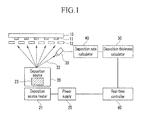
- FIG. 1 is a block diagram of a device for manufacturing a display device construct as the principle of an exemplary embodiment of the present invention.
- FIGS. 2A and 2B are flowcharts of methods for manufacturing a display device construct as the principle of an exemplary embodiment of the present invention.
- FIG. 3 is a block diagram of a device for manufacturing a display device construct as the principle of another exemplary embodiment of the present invention.
- FIGS. 4A and 4B are flowcharts of methods for manufacturing a display device construct as the principle of another exemplary embodiment of the present invention.
- FIG. 5 is a cross-sectional view of an organic light emitting element manufactured by a device and a method for manufacturing a display device construct as the principle of an exemplary embodiment of the present invention.
- FIG. 6A is a two dimensional graph showing change of deposition source heater power as a function of time in a deposition device using a contemporary PID controller.
- FIG. 6B is a two dimensional graph showing change of distribution of deposition thickness as a function of frequency in a deposition device using a contemporary PID controller.
- FIG. 7A is a two dimensional graph showing change of deposition source heater power as a function of time in a device for manufacturing a display device construct as an exemplary embodiment of the present invention.
- FIG. 7B is a two dimensional graph showing change of the distribution of deposition thickness as a function of frequency in a device for manufacturing a display device construct as the principle of an exemplary embodiment of the present invention.
- FIG. 8A is a two dimensional graph showing change of deposition source heater power as a function of time in a device for manufacturing a display device construct as the principle of another exemplary embodiment of the present invention.
- FIG. 8B is a two dimensional graph showing change of the distribution of deposition thickness as a function of frequency in a device for manufacturing a display device construct as the principle of another exemplary embodiment of the present invention.
- a plurality of thin films included in the flat panel displays may be formed by a deposition process.
- each of thin films may be measured to determine whether the each of the thin films is formed to have a predetermined reference thickness, and a deposition ratio may be corrected if the actual thickness is different from the predetermined reference thickness.
- a deposition material received in a deposition vessel may be heated to become in form of vapor in a sublimation state, the deposition material in form of vapor is absorbed by a substrate surface, and deposition absorbed is formed as a thin film on the substrate.
- a quartz crystal sensor may measure the actual deposition speed of the deposition material that is received by the deposition vessel, heated, changed into a vapor form in the sublimation state, and vaporized.
- the actual deposition speed measured by the quartz crystal sensor may be compared with a predetermined deposition speed.
- the actual thickness of the thin film formed on the deposited substrate may be also compared with the predetermined reference thickness. When the actual thickness is different from the predetermined reference thickness, the deposition ratio may be corrected.
- the actual thickness of the thin film may be indirectly checked by using the quartz crystal sensor instead of directly measuring the actual thickness of the thin film formed on the substrate.
- the quartz crystal sensor may include a measurement noise as time passes, because, for example, the resonant frequency of the quartz crystal sensor may change due to the measurement noise as time passes.
- power of a heater for heating the deposition vessel may be controlled by a PID (proportional integral derivative) controller.
- the PID controller is a generic control loop feedback controller used in industrial control systems.
- the response performance may be worsened by disturbance.
- the PID control method compares a deviation for an abrupt disturbance. When a large deviation occurs, the PID control method increases a manipulated variable to quickly reach the target value.
- power of the heater is controlled by the PID control method, power of the heater may be substantially changed, and performance of devices may be degraded.
- FIG. 1 is a block diagram of a device for manufacturing a display device constructed as the principle of an exemplary embodiment of the present invention
- FIGS. 2A and 2B are flowcharts of methods for manufacturing a display device constructed as the principle of an exemplary embodiment of the present invention.
- the display device manufacturing device includes a deposition source 20 , a deposition speed measuring sensor 30 , a deposition rate calculator 40 , a deposition thickness calculator 50 , and a real-time controller 60 .
- the deposition source 20 includes a deposition material 23 , and the deposition source 20 is connected to a deposition chamber (not shown) in which the deposition process is performed.
- the deposition material that is formed as an organic thin film layer of an organic light emitting element includes a hole injection material, a hole transport material, a light emitting material, an electron transport material, and an electron injection material.
- the hole injection material helps easy injection of holes from an anode, and copper phthalocyanine (CuPc) or PEDOT is generally used.
- the hole transport material easily carries the holes and binds the electrons in the light emitting area in order to increase the exciton formation possibility, and an amine for stabilizing positive ion radicals is used.
- the electron transport material represents a compound that has electron withdrawers for stabilizing the negative ion radicals generated when electrons are injected from a cathode, or a metallic compound for receiving the electrons.
- the compounds including a functional group withdrawing the electrons by resonance include a cyano group, an oxadiazole, or a triazole, and the compound such as Alq3 (Al(C9H6NO)3) may be used.
- the electron injection material represents a metal compound having electron affinity to control the electrons to be fluently injected from the cathode.
- the light emitting material may emit three primary colors of red, green, and blue.
- the blue light emitting material may use anthracene, phenyl-replaced cyclopentadiene, and DVPBi.
- the green light emitting material may use Alq3, and the red light emitting material may use perylene.
- a deposition source heater 21 is provided close to the deposition source 20 , and the deposition source heater 21 sublimates the deposition material by heating the deposition source 20 .
- the deposition source heater 21 is electrically connected to a power supply 25 , and the power supply 25 supplies power to the deposition source heater 21 .
- the deposition speed measuring sensor 30 is provided in the deposition chamber, and measures a vapor volume 22 of the sublimated deposition material of the deposition source 20 .
- the deposition speed is in proportion to the vapor volume 22 of the deposition material filling the deposition chamber. That is, the deposition speed may be calculated by measuring the vapor volume 22 of the deposition material in the deposition chamber.
- the quartz crystal sensor may be used as the deposition speed measuring sensor 30 .
- the deposition rate calculator 40 is connected to the deposition speed measuring sensor 30 , and calculates the deposition speed by using the measured vapor volume 22 of the deposition material.
- the deposition thickness calculator 50 is connected to the deposition rate calculator 40 , and calculates the deposition thickness by integrating the deposition speed of the calculated deposition material.
- the real-time controller 60 is connected to the deposition thickness calculator 50 , and controls the amount of power supplied by the power supply 25 of the deposition source heater 21 by comparing the calculated deposition thickness with a reference thickness.
- the substrate 10 is loaded into the deposition chamber (S 110 ).
- the deposition material that is sublimated from the deposition source 20 passes through a mask 12 and the deposition material is deposited on a substrate 10 to form a thin film 11 (S 120 ).
- the deposition speed is determined by the deposition speed measuring sensor 30 and the deposition rate calculator 40 (S 130 ).
- the deposition speed measuring sensor 30 measures the vapor volume 22 of the deposition material in the deposition chamber (S 131 ), and the deposition rate calculator 40 calculates the deposition speed of the deposition material by using the vapor volume 22 of the deposition material measured by the deposition speed measuring sensor 30 (S 132 ).
- the quartz crystal sensor When the quartz crystal sensor is adopted as the deposition speed measuring sensor 30 , the quartz crystal sensor measures the resonant frequency of the quartz crystal when the quartz crystal vibrates at several MHz by an oscillator (not shown). The vapor volume 22 of the deposition material may be measured from the resonant frequency of the quartz crystal.
- the deposition rate calculator 40 may calculate the deposition speed of the deposition material, in consideration of the type of deposition material, density, and other characteristics. The deposition rate calculator 40 transmits the calculated deposition speed to the deposition thickness calculator 50 .
- the deposition thickness calculator 50 integrates the deposition speed calculated by the deposition rate calculator 40 with respect to time in order to calculate the actual deposition thickness of the deposited thin film 11 , that is, the actual thickness of the deposition material deposited on the substrate 10 (S 140 ).
- the deposition thickness calculator 50 transmits the calculated deposition thickness of the deposition material to the real-time controller 60 .
- the real-time controller 60 controls power of the deposition source heater 21 by comparing the calculated deposition thickness with a reference thickness (S 150 ).
- the real-time controller 60 includes the reference thickness of the thin film 11 .
- the real-time controller 60 compares the actual deposition thickness calculated from measurement of the deposition speed with the reference thickness, increases the amount of power supplied by the power supply 25 of the deposition source heater 21 when the actual deposition thickness is less than the reference thickness, and reduces the amount of power supplied by the power supply 25 of the deposition source heater 21 when the actual deposition thickness is greater than the reference thickness. That is, the real-time controller 60 controls the amount of power supplied by the power supply 25 of the deposition source heater 21 in real-time.
- measurement of vapor volume 22 of the deposition material by the deposition speed measuring sensor 30 calculation of the deposition speed by the deposition rate calculator 40 , calculation of the deposition thickness by the deposition thickness calculator 50 , and control of the amount of power supplied by the power supply 25 of the real-time controller 60 are performed for each substrate on which a thin film 11 is to be deposited. That is, deposition speed measurement, deposition thickness calculation, and control of the amount of power supplied by the power supply 25 of the deposition source heater 21 are performed upon a substrate is loaded into the deposition chamber, and the deposition process for forming the thin film is then performed.
- the influence of measurement noise that may be generated by the deposition speed measuring sensor 30 may be minimized, and distribution of the deposition thickness of the organic light emitting material may be reduced.
- FIG. 3 is a block diagram of a device for manufacturing a display device constructed as another exemplary embodiment of the present invention
- FIGS. 4A and 4B are flowcharts of methods for manufacturing a display device constructed as another exemplary embodiment of the present invention.
- the device for manufacturing a display device includes a deposition source 120 , a deposition thickness measurer 130 , a deposition thickness calculator 140 , and a real-time controller 160 .
- the deposition source 120 includes a deposition material, and the deposition source 120 is connected to a deposition chamber (not shown) in which the deposition process is performed.
- the deposition material that is formed as an organic thin film layer of an organic light emitting element includes a hole injection material, a hole transport material, a light emitting material, an electron transport material, and an electron injection material.
- a deposition source heater 121 is provided near the deposition source 120 , and the deposition source heater 121 is connected to a power supply 125 .
- the deposition thickness measurer 130 includes a photo-irradiator 131 and a photo-receiver 132 installed in the deposition chamber.
- the photo-irradiator 131 irradiates light onto a pattern of a thin film 111 deposited on a substrate 110
- the photo-receiver 132 receives the light reflected from a pattern of the thin film 111 and measures a polarization state of the reflected light.
- An ellipsometer may be used for the deposition thickness measurer 130 .
- the deposition thickness calculator 140 is connected to the deposition thickness measurer 130 , and calculates the deposition thickness from the polarization state of the reflected light.
- the real-time controller 160 is connected to the deposition thickness calculator 140 , and compares the calculated deposition thickness with a reference thickness to control the amount of power supplied by the power supply 125 of the deposition source heater 121 .
- the substrate 110 is loaded into the deposition chamber (S 210 ).
- the deposition material that is sublimated from the deposition source 120 passes through a mask 112 and the deposition material is deposited on the substrate 110 to form a thin film 111 (S 220 ).
- the deposition thickness is measured by the deposition thickness measurer 130 at regular intervals (S 230 ).
- the photo-irradiator 131 irradiates light onto a random pattern of the thin film 111 for each predetermined period (S 231 ), and the photo-receiver 132 receives the light reflected from the random pattern of the thin film 111 and measures a polarization state of the reflected light (S 232 ).
- the deposition thickness calculator 140 calculates the deposition thickness by using the measured polarization state of the reflected light (S 233 ).
- the random pattern of the thin film 111 is a measurement pattern additionally prepared for measuring the thickness of the thin film 111 , and the random pattern may be a separate pattern that is deposited when the deposition material is deposited on the substrate 110 .
- Polarization of light reflected on the random pattern of the thin film 111 varies with the thickness of the deposited thin film 111 , and the photo-receiver 132 measures the polarization state of the reflected light.
- the photo-receiver 132 transmits the polarization state of the reflected light to the deposition thickness calculator 140 , and the deposition thickness calculator 140 calculates the deposition thickness of the deposition material from the polarization state of the reflected light.
- the deposition thickness calculator 140 transmits the calculated deposition thickness of the deposition material to the real-time controller 160 .
- the real-time controller 160 controls power of the deposition source heater 121 by comparing the calculated deposition thickness with a reference thickness (S 240 ).
- the real-time controller 160 includes the reference thickness of the thin film 111 .
- the real-time controller 160 compares the measured actual deposition thickness with the reference thickness, increases the amount of power supplied by the power supply 125 of the deposition source heater 121 when the actual deposition thickness is less than the reference thickness, and reduces the amount of power supplied by the power supply 125 of the deposition source heater 121 when the actual deposition thickness is greater than the reference thickness.
- the real-time controller 160 controls the amount of power supplied by the power supply 125 of the deposition source heater 121 in real-time by using the actual deposition thickness that is measured for each predetermined period during the deposition process of the thin film 111 .
- measurement of the deposition thickness by the deposition thickness measurer 130 and the deposition thickness calculator 140 and control of the amount of power supplied by the power supply 125 of the real-time controller 160 , are performed for each predetermined period.
- a determination (S 250 ) is made to determine whether the deposition process of the thin film 111 is completed. If the deposition process is not completed, the steps of determining deposition thickness and controlling power of deposition source heater are repeated.
- FIG. 5 is a cross-sectional view of an organic light emitting element manufactured by a device for manufacturing a display device according to an exemplary embodiment of the present invention.
- the organic light emitting element includes an organic thin film layer 211 that is deposited on a substrate 210 .
- the organic thin film layer 211 includes a hole injection layer (HIL) 211 a , a hole transport layer 211 b , an emission layer 211 c , an electron transport layer 211 d , and an electron injection layer (EIL) 211 e that are sequentially provided on the substrate 210 .
- the organic thin film layer 211 may be provided when a hole injection material, a hole transport material, a light emitting material, an electron transport material, and an electron injection material are sequentially deposited on the substrate 210 .
- An anode may be formed below the hole injection layer (HIL) 211 a , and a cathode (not shown) may be formed above the electron injection layer (EIL) 211 e .
- the anode has a work function that is greater than that of the cathode, and is formed with a material for transmitting visible light generated by the organic thin film layer 211 to the outside.
- the work function is the minimum energy (usually measured in electron volts) needed to remove an electron from a solid to a point immediately outside the solid surface (or the minimum energy needed to move an electron from the Fermi level into vacuum).
- ITO indium-tin oxide
- the cathode may be made with metallic materials having high reflectance, such as gold (Au), copper (Cu), aluminum (Al), silver (Ag), indium (In), calcium (Ca), or alloys thereof.
- FIG. 6A is a graph showing change of deposition source heater power as a function of time in a deposition device using a conventional PID controller.
- FIG. 6B is a graph showing change of distribution of deposition thickness as a function of frequency in a deposition device using a conventional PID controller.
- the contemporary deposition device determines the deposition speed of the deposition material by using the vapor volume 22 of the deposition material measured by the quartz crystal sensor, and controls power of the deposition source heater 21 by using the PID controller according to the deposition speed.
- the power variation graph of the deposition source heater 21 shows variation of power of the deposition source heater with respect to time, wherein the horizontal axis indicates time (sec) and the vertical axis indicates power amount (%).
- the distribution graph of the deposition thickness shows distribution of thickness of the thin film deposited on the substrate, the horizontal axis shows thickness ( ⁇ ) of the deposited thin film, and the vertical axis shows frequency.
- the power variation graph of the deposition source heater shows that the power of the deposition source heater is fluctuated.
- the distribution graph of the deposition thickness shows distribution of the deposition thickness as 2.04 ⁇ .
- FIG. 7A is a graph showing the change of deposition source heater power as a function of time in a device for manufacturing a display device constructed as an exemplary embodiment of the present invention.
- FIG. 7B is a graph showing the change of the distribution of deposition thickness as a function of frequency in a device for manufacturing a display device constructed as an exemplary embodiment of the present invention.
- the distribution graph of the deposition thickness shows that the distribution of the deposition thickness is 1.10 ⁇ .
- the distribution of deposition thickness of FIG. 7B is much less compared to that of FIG. 6B .
- FIG. 8A is a graph showing change of deposition source heater power as a function of time in a device for manufacturing a display device according to another exemplary embodiment of the present invention.
- FIG. 8B is a graph showing change of the distribution of deposition thickness as a function of frequency in a device for manufacturing a display device according to another exemplary embodiment of the present invention.
- the distribution graph of the deposition thickness shows that the distribution of the deposition thickness is 0.50 ⁇ .
- the distribution of deposition thickness of FIG. 8B is much less compared to that of FIG. 6B .
- the case of calculation/measuring the deposition thickness and controlling the power of the deposition source heater by using the real-time controller of the present invention provides a more stable power variation of the deposition source heater and shows that the distribution of the deposition thickness is much less and the actual thickness is much closer to the reference thickness compared with the contemporary case. That is, the yield of the deposition process may be increased and a higher quality display device may be produced by reducing the distribution of the deposition thickness of the organic light emitting material.
Landscapes
- Chemical & Material Sciences (AREA)
- Chemical Kinetics & Catalysis (AREA)
- Engineering & Computer Science (AREA)
- Materials Engineering (AREA)
- Mechanical Engineering (AREA)
- Metallurgy (AREA)
- Organic Chemistry (AREA)
- General Chemical & Material Sciences (AREA)
- Electroluminescent Light Sources (AREA)
Abstract
Description
Claims (3)
Applications Claiming Priority (2)
| Application Number | Priority Date | Filing Date | Title |
|---|---|---|---|
| KR1020100009718A KR101094307B1 (en) | 2010-02-02 | 2010-02-02 | Apparatus and method for manufacturing a display device |
| KR10-2010-0009718 | 2010-02-02 |
Publications (2)
| Publication Number | Publication Date |
|---|---|
| US20110189380A1 US20110189380A1 (en) | 2011-08-04 |
| US8899174B2 true US8899174B2 (en) | 2014-12-02 |
Family
ID=44341920
Family Applications (1)
| Application Number | Title | Priority Date | Filing Date |
|---|---|---|---|
| US12/896,496 Expired - Fee Related US8899174B2 (en) | 2010-02-02 | 2010-10-01 | Device and method for fabricating display device |
Country Status (2)
| Country | Link |
|---|---|
| US (1) | US8899174B2 (en) |
| KR (1) | KR101094307B1 (en) |
Families Citing this family (6)
| Publication number | Priority date | Publication date | Assignee | Title |
|---|---|---|---|---|
| KR101959975B1 (en) | 2012-07-10 | 2019-07-16 | 삼성디스플레이 주식회사 | Apparatus for organic layer deposition, method for manufacturing of organic light emitting display apparatus using the same, and organic light emitting display apparatus manufactured by the method |
| KR102108361B1 (en) * | 2013-06-24 | 2020-05-11 | 삼성디스플레이 주식회사 | Apparatus for monitoring deposition rate, apparatus for organic layer deposition using the same, method for monitoring deposition rate, and method for manufacturing of organic light emitting display apparatus using the same |
| US9657391B2 (en) | 2014-05-08 | 2017-05-23 | Halliburton Energy Services, Inc. | Optical transmission/reflection mode in-situ deposition rate control for ice fabrication |
| KR20220129598A (en) | 2020-01-22 | 2022-09-23 | 어플라이드 머티어리얼스, 인코포레이티드 | In-line monitoring of OLED layer thickness and dopant concentration |
| KR102778467B1 (en) | 2020-01-22 | 2025-03-06 | 어플라이드 머티어리얼스, 인코포레이티드 | In-line monitoring of OLED layer thickness and dopant concentration |
| US12163783B2 (en) * | 2021-04-21 | 2024-12-10 | Applied Materials, Inc. | Digital holography for alignment in layer deposition |
Citations (15)
| Publication number | Priority date | Publication date | Assignee | Title |
|---|---|---|---|---|
| US4627989A (en) * | 1983-08-20 | 1986-12-09 | Leybold Heraeus Gmbh | Method and system for a vacuum evaporative deposition process |
| US6040939A (en) * | 1998-06-16 | 2000-03-21 | Turkiye Sise Ve Cam Fabrikalari A.S. | Anti-solar and low emissivity functioning multi-layer coatings on transparent substrates |
| US6060826A (en) * | 1997-03-19 | 2000-05-09 | Minolta Co., Ltd. | Organic electroluminescent element having an excimer light irradiated positive electrode and method of manufacturing the same |
| US20020153360A1 (en) * | 2001-04-20 | 2002-10-24 | Semiconductor Energy Laboratory Co., Ltd. | Laser irradiating apparatus and method of manufacturing semiconductor apparatus |
| US20030136772A1 (en) * | 2001-10-30 | 2003-07-24 | Shunpei Yamazaki | Laser apparatus, laser irradiation method, manufacturing method for semiconductor device, semiconductor device, production system for semiconductor device using the laser apparatus, and electronic equipment |
| JP2004225058A (en) | 2002-11-29 | 2004-08-12 | Sony Corp | Film forming apparatus and display panel manufacturing apparatus and method |
| KR20050051138A (en) | 2003-11-27 | 2005-06-01 | 삼성에스디아이 주식회사 | Method of vacuum evaporation and apparatus the same |
| KR20060080679A (en) | 2005-01-06 | 2006-07-11 | 삼성에스디아이 주식회사 | Control Method of Deposition Source of Deposition System |
| US20070221131A1 (en) * | 2006-03-22 | 2007-09-27 | Canon Kabushiki Kaisha | Vapor deposition source and vapor deposition apparatus |
| KR20080002189A (en) | 2006-06-30 | 2008-01-04 | 세메스 주식회사 | Source Shutter and Substrate Control Method of Organic Light-Emitting Device Deposition Equipment |
| US20080098957A1 (en) * | 2006-10-30 | 2008-05-01 | Seung-Yoon Ryu | Deposition apparatus and method |
| KR20080046954A (en) | 2006-11-24 | 2008-05-28 | 세메스 주식회사 | Organic thin film deposition apparatus |
| KR20080062168A (en) | 2006-12-29 | 2008-07-03 | 엘지디스플레이 주식회사 | Apparatus and method for manufacturing flat panel display |
| KR20080081684A (en) | 2007-03-06 | 2008-09-10 | 세메스 주식회사 | Organic thin film thickness measuring unit, organic thin film deposition apparatus having the same, organic thin film thickness measuring method |
| US20100086681A1 (en) | 2007-03-06 | 2010-04-08 | Tokyo Electron Limited | Control device of evaporating apparatus and control method of evaporating apparatus |
-
2010
- 2010-02-02 KR KR1020100009718A patent/KR101094307B1/en not_active Expired - Fee Related
- 2010-10-01 US US12/896,496 patent/US8899174B2/en not_active Expired - Fee Related
Patent Citations (18)
| Publication number | Priority date | Publication date | Assignee | Title |
|---|---|---|---|---|
| US4627989A (en) * | 1983-08-20 | 1986-12-09 | Leybold Heraeus Gmbh | Method and system for a vacuum evaporative deposition process |
| US6060826A (en) * | 1997-03-19 | 2000-05-09 | Minolta Co., Ltd. | Organic electroluminescent element having an excimer light irradiated positive electrode and method of manufacturing the same |
| US6040939A (en) * | 1998-06-16 | 2000-03-21 | Turkiye Sise Ve Cam Fabrikalari A.S. | Anti-solar and low emissivity functioning multi-layer coatings on transparent substrates |
| US20020153360A1 (en) * | 2001-04-20 | 2002-10-24 | Semiconductor Energy Laboratory Co., Ltd. | Laser irradiating apparatus and method of manufacturing semiconductor apparatus |
| US20050277028A1 (en) * | 2001-10-30 | 2005-12-15 | Semiconductor Energy Laboratory Co., Ltd. | Laser apparatus, laser irradiation method, manufacturing method for semiconductor device, semiconductor device, production system for semiconductor device using the laser apparatus, and electronic equipment |
| US20040132266A1 (en) * | 2001-10-30 | 2004-07-08 | Semiconductor Energy Laboratory Co., Ltd. | Laser apparatus, laser irradiation method, manufacturing method for semiconductor device, semiconductor device, production system for semiconductor device using the laser apparatus, and electronic equipment |
| US20030136772A1 (en) * | 2001-10-30 | 2003-07-24 | Shunpei Yamazaki | Laser apparatus, laser irradiation method, manufacturing method for semiconductor device, semiconductor device, production system for semiconductor device using the laser apparatus, and electronic equipment |
| JP2004225058A (en) | 2002-11-29 | 2004-08-12 | Sony Corp | Film forming apparatus and display panel manufacturing apparatus and method |
| KR20050051138A (en) | 2003-11-27 | 2005-06-01 | 삼성에스디아이 주식회사 | Method of vacuum evaporation and apparatus the same |
| KR20060080679A (en) | 2005-01-06 | 2006-07-11 | 삼성에스디아이 주식회사 | Control Method of Deposition Source of Deposition System |
| US20070221131A1 (en) * | 2006-03-22 | 2007-09-27 | Canon Kabushiki Kaisha | Vapor deposition source and vapor deposition apparatus |
| KR20080002189A (en) | 2006-06-30 | 2008-01-04 | 세메스 주식회사 | Source Shutter and Substrate Control Method of Organic Light-Emitting Device Deposition Equipment |
| US20080098957A1 (en) * | 2006-10-30 | 2008-05-01 | Seung-Yoon Ryu | Deposition apparatus and method |
| KR20080038671A (en) | 2006-10-30 | 2008-05-07 | 삼성에스디아이 주식회사 | Deposition apparatus and deposition method capable of measuring the thickness of the deposited film in real time |
| KR20080046954A (en) | 2006-11-24 | 2008-05-28 | 세메스 주식회사 | Organic thin film deposition apparatus |
| KR20080062168A (en) | 2006-12-29 | 2008-07-03 | 엘지디스플레이 주식회사 | Apparatus and method for manufacturing flat panel display |
| KR20080081684A (en) | 2007-03-06 | 2008-09-10 | 세메스 주식회사 | Organic thin film thickness measuring unit, organic thin film deposition apparatus having the same, organic thin film thickness measuring method |
| US20100086681A1 (en) | 2007-03-06 | 2010-04-08 | Tokyo Electron Limited | Control device of evaporating apparatus and control method of evaporating apparatus |
Also Published As
| Publication number | Publication date |
|---|---|
| KR20110090121A (en) | 2011-08-10 |
| KR101094307B1 (en) | 2011-12-19 |
| US20110189380A1 (en) | 2011-08-04 |
Similar Documents
| Publication | Publication Date | Title |
|---|---|---|
| US8899174B2 (en) | Device and method for fabricating display device | |
| TWI539637B (en) | Vacuum vapor deposition system | |
| TWI433947B (en) | Vacuum vapor deposition system | |
| JP4436920B2 (en) | Organic vapor deposition source and method for controlling the heating source | |
| JP2010196082A (en) | Vacuum vapor deposition apparatus | |
| US9458532B2 (en) | Vapor deposition method and vapor deposition apparatus | |
| JP6139423B2 (en) | Vapor deposition apparatus, vapor deposition method, and organic electroluminescence element manufacturing method | |
| JP2015519477A (en) | Sputtering method for pre-stabilized plasma processing | |
| US20060185588A1 (en) | Vapor deposition apparatus measuring film thickness by irradiating light | |
| JP2012012689A (en) | Method and apparatus for vacuum evaporation | |
| KR20150113742A (en) | Evaporation source and deposition apparatus including the same | |
| KR101286523B1 (en) | Apparatus and method for fabricating flat display | |
| JP4611884B2 (en) | Vapor deposition film thickness measuring method and vapor deposition system | |
| JP2000294372A (en) | Formation of organic material film, manufacture of organic el element and device therefor | |
| JP3719797B2 (en) | Method for forming conductive thin film on organic thin film surface | |
| US20060147628A1 (en) | Controlling effusion cell of deposition system | |
| CN1800434B (en) | Method of controlling an injector of a deposition system | |
| KR20060068682A (en) | Manufacturing apparatus and manufacturing method of organic electroluminescent display device | |
| JP2014065942A (en) | Vacuum evaporation device | |
| KR100709265B1 (en) | Organic material deposition apparatus and deposition method | |
| KR20180027140A (en) | Apparatus and Method for controlling film-thickness in inline-type vapor deposition process | |
| KR102253290B1 (en) | Deposition Dectecting Sensor and depositing velocity measuring device and thin film depositing apparatus | |
| KR100684739B1 (en) | Organic material deposition apparatus | |
| JP2005340225A (en) | Organic EL device | |
| KR100786844B1 (en) | Equipment for manufacturing organic light emitting display |
Legal Events
| Date | Code | Title | Description |
|---|---|---|---|
| AS | Assignment |
Owner name: SAMSUNG MOBILE DISPLAY CO., LTD., A CORPORATION CH Free format text: ASSIGNMENT OF ASSIGNORS INTEREST;ASSIGNORS:JANG, WON-HYOUK;KANG, EU-GENE;LEE, JOO-HWA;AND OTHERS;REEL/FRAME:025228/0349 Effective date: 20100826 |
|
| AS | Assignment |
Owner name: SAMSUNG DISPLAY CO., LTD., KOREA, REPUBLIC OF Free format text: DIVERSTITURE;ASSIGNOR:SAMSUNG MOBILE DISPLAY CO., LTD.;REEL/FRAME:029087/0636 Effective date: 20120702 Owner name: SAMSUNG DISPLAY CO., LTD., KOREA, REPUBLIC OF Free format text: MERGER;ASSIGNOR:SAMSUNG MOBILE DISPLAY CO., LTD.;REEL/FRAME:029087/0636 Effective date: 20120702 |
|
| STCF | Information on status: patent grant |
Free format text: PATENTED CASE |
|
| FEPP | Fee payment procedure |
Free format text: PAYOR NUMBER ASSIGNED (ORIGINAL EVENT CODE: ASPN); ENTITY STATUS OF PATENT OWNER: LARGE ENTITY |
|
| MAFP | Maintenance fee payment |
Free format text: PAYMENT OF MAINTENANCE FEE, 4TH YEAR, LARGE ENTITY (ORIGINAL EVENT CODE: M1551) Year of fee payment: 4 |
|
| FEPP | Fee payment procedure |
Free format text: MAINTENANCE FEE REMINDER MAILED (ORIGINAL EVENT CODE: REM.); ENTITY STATUS OF PATENT OWNER: LARGE ENTITY |
|
| LAPS | Lapse for failure to pay maintenance fees |
Free format text: PATENT EXPIRED FOR FAILURE TO PAY MAINTENANCE FEES (ORIGINAL EVENT CODE: EXP.); ENTITY STATUS OF PATENT OWNER: LARGE ENTITY |
|
| STCH | Information on status: patent discontinuation |
Free format text: PATENT EXPIRED DUE TO NONPAYMENT OF MAINTENANCE FEES UNDER 37 CFR 1.362 |
|
| FP | Lapsed due to failure to pay maintenance fee |
Effective date: 20221202 |