US8830148B2 - Organic electroluminescence display device and organic electroluminescence display device manufacturing method - Google Patents
Organic electroluminescence display device and organic electroluminescence display device manufacturing method Download PDFInfo
- Publication number
- US8830148B2 US8830148B2 US13/403,375 US201213403375A US8830148B2 US 8830148 B2 US8830148 B2 US 8830148B2 US 201213403375 A US201213403375 A US 201213403375A US 8830148 B2 US8830148 B2 US 8830148B2
- Authority
- US
- United States
- Prior art keywords
- voltage
- luminance
- capacitor
- driver
- correction parameter
- Prior art date
- Legal status (The legal status is an assumption and is not a legal conclusion. Google has not performed a legal analysis and makes no representation as to the accuracy of the status listed.)
- Expired - Fee Related, expires
Links
Images


Classifications
-
- H01L27/3276—
-
- G—PHYSICS
- G09—EDUCATION; CRYPTOGRAPHY; DISPLAY; ADVERTISING; SEALS
- G09G—ARRANGEMENTS OR CIRCUITS FOR CONTROL OF INDICATING DEVICES USING STATIC MEANS TO PRESENT VARIABLE INFORMATION
- G09G3/00—Control arrangements or circuits, of interest only in connection with visual indicators other than cathode-ray tubes
- G09G3/20—Control arrangements or circuits, of interest only in connection with visual indicators other than cathode-ray tubes for presentation of an assembly of a number of characters, e.g. a page, by composing the assembly by combination of individual elements arranged in a matrix no fixed position being assigned to or needed to be assigned to the individual characters or partial characters
- G09G3/22—Control arrangements or circuits, of interest only in connection with visual indicators other than cathode-ray tubes for presentation of an assembly of a number of characters, e.g. a page, by composing the assembly by combination of individual elements arranged in a matrix no fixed position being assigned to or needed to be assigned to the individual characters or partial characters using controlled light sources
- G09G3/30—Control arrangements or circuits, of interest only in connection with visual indicators other than cathode-ray tubes for presentation of an assembly of a number of characters, e.g. a page, by composing the assembly by combination of individual elements arranged in a matrix no fixed position being assigned to or needed to be assigned to the individual characters or partial characters using controlled light sources using electroluminescent panels
- G09G3/32—Control arrangements or circuits, of interest only in connection with visual indicators other than cathode-ray tubes for presentation of an assembly of a number of characters, e.g. a page, by composing the assembly by combination of individual elements arranged in a matrix no fixed position being assigned to or needed to be assigned to the individual characters or partial characters using controlled light sources using electroluminescent panels semiconductive, e.g. using light-emitting diodes [LED]
- G09G3/3208—Control arrangements or circuits, of interest only in connection with visual indicators other than cathode-ray tubes for presentation of an assembly of a number of characters, e.g. a page, by composing the assembly by combination of individual elements arranged in a matrix no fixed position being assigned to or needed to be assigned to the individual characters or partial characters using controlled light sources using electroluminescent panels semiconductive, e.g. using light-emitting diodes [LED] organic, e.g. using organic light-emitting diodes [OLED]
- G09G3/3225—Control arrangements or circuits, of interest only in connection with visual indicators other than cathode-ray tubes for presentation of an assembly of a number of characters, e.g. a page, by composing the assembly by combination of individual elements arranged in a matrix no fixed position being assigned to or needed to be assigned to the individual characters or partial characters using controlled light sources using electroluminescent panels semiconductive, e.g. using light-emitting diodes [LED] organic, e.g. using organic light-emitting diodes [OLED] using an active matrix
- G09G3/3233—Control arrangements or circuits, of interest only in connection with visual indicators other than cathode-ray tubes for presentation of an assembly of a number of characters, e.g. a page, by composing the assembly by combination of individual elements arranged in a matrix no fixed position being assigned to or needed to be assigned to the individual characters or partial characters using controlled light sources using electroluminescent panels semiconductive, e.g. using light-emitting diodes [LED] organic, e.g. using organic light-emitting diodes [OLED] using an active matrix with pixel circuitry controlling the current through the light-emitting element
-
- H—ELECTRICITY
- H10—SEMICONDUCTOR DEVICES; ELECTRIC SOLID-STATE DEVICES NOT OTHERWISE PROVIDED FOR
- H10K—ORGANIC ELECTRIC SOLID-STATE DEVICES
- H10K59/00—Integrated devices, or assemblies of multiple devices, comprising at least one organic light-emitting element covered by group H10K50/00
- H10K59/10—OLED displays
- H10K59/12—Active-matrix OLED [AMOLED] displays
- H10K59/121—Active-matrix OLED [AMOLED] displays characterised by the geometry or disposition of pixel elements
- H10K59/1216—Active-matrix OLED [AMOLED] displays characterised by the geometry or disposition of pixel elements the pixel elements being capacitors
-
- H—ELECTRICITY
- H10—SEMICONDUCTOR DEVICES; ELECTRIC SOLID-STATE DEVICES NOT OTHERWISE PROVIDED FOR
- H10K—ORGANIC ELECTRIC SOLID-STATE DEVICES
- H10K59/00—Integrated devices, or assemblies of multiple devices, comprising at least one organic light-emitting element covered by group H10K50/00
- H10K59/10—OLED displays
- H10K59/12—Active-matrix OLED [AMOLED] displays
- H10K59/131—Interconnections, e.g. wiring lines or terminals
-
- H—ELECTRICITY
- H10—SEMICONDUCTOR DEVICES; ELECTRIC SOLID-STATE DEVICES NOT OTHERWISE PROVIDED FOR
- H10K—ORGANIC ELECTRIC SOLID-STATE DEVICES
- H10K71/00—Manufacture or treatment specially adapted for the organic devices covered by this subclass
- H10K71/70—Testing, e.g. accelerated lifetime tests
-
- G06G2360/147—
-
- G—PHYSICS
- G09—EDUCATION; CRYPTOGRAPHY; DISPLAY; ADVERTISING; SEALS
- G09G—ARRANGEMENTS OR CIRCUITS FOR CONTROL OF INDICATING DEVICES USING STATIC MEANS TO PRESENT VARIABLE INFORMATION
- G09G2300/00—Aspects of the constitution of display devices
- G09G2300/08—Active matrix structure, i.e. with use of active elements, inclusive of non-linear two terminal elements, in the pixels together with light emitting or modulating elements
- G09G2300/0809—Several active elements per pixel in active matrix panels
- G09G2300/0819—Several active elements per pixel in active matrix panels used for counteracting undesired variations, e.g. feedback or autozeroing
-
- G—PHYSICS
- G09—EDUCATION; CRYPTOGRAPHY; DISPLAY; ADVERTISING; SEALS
- G09G—ARRANGEMENTS OR CIRCUITS FOR CONTROL OF INDICATING DEVICES USING STATIC MEANS TO PRESENT VARIABLE INFORMATION
- G09G2300/00—Aspects of the constitution of display devices
- G09G2300/08—Active matrix structure, i.e. with use of active elements, inclusive of non-linear two terminal elements, in the pixels together with light emitting or modulating elements
- G09G2300/0809—Several active elements per pixel in active matrix panels
- G09G2300/0842—Several active elements per pixel in active matrix panels forming a memory circuit, e.g. a dynamic memory with one capacitor
- G09G2300/0852—Several active elements per pixel in active matrix panels forming a memory circuit, e.g. a dynamic memory with one capacitor being a dynamic memory with more than one capacitor
-
- G—PHYSICS
- G09—EDUCATION; CRYPTOGRAPHY; DISPLAY; ADVERTISING; SEALS
- G09G—ARRANGEMENTS OR CIRCUITS FOR CONTROL OF INDICATING DEVICES USING STATIC MEANS TO PRESENT VARIABLE INFORMATION
- G09G2320/00—Control of display operating conditions
- G09G2320/04—Maintaining the quality of display appearance
- G09G2320/043—Preventing or counteracting the effects of ageing
-
- G—PHYSICS
- G09—EDUCATION; CRYPTOGRAPHY; DISPLAY; ADVERTISING; SEALS
- G09G—ARRANGEMENTS OR CIRCUITS FOR CONTROL OF INDICATING DEVICES USING STATIC MEANS TO PRESENT VARIABLE INFORMATION
- G09G2360/00—Aspects of the architecture of display systems
- G09G2360/14—Detecting light within display terminals, e.g. using a single or a plurality of photosensors
- G09G2360/145—Detecting light within display terminals, e.g. using a single or a plurality of photosensors the light originating from the display screen
- G09G2360/147—Detecting light within display terminals, e.g. using a single or a plurality of photosensors the light originating from the display screen the originated light output being determined for each pixel
-
- H01L27/3265—
Definitions
- the present invention relates to an organic electroluminescence display device and an organic electroluminescence display device manufacturing method.
- Image display devices using organic electroluminescence elements (OLED: Organic Light-Emitting Diodes) are well-known as image display devices using current-driven light-emitting elements. Due to such advantages as excellent viewing angle characteristics and low power consumption, such organic EL displays have gained much attention as candidates for next-generation flat panel displays (FPDs).
- OLED Organic Light-Emitting Diodes
- organic EL elements included in pixels are normally arranged in a matrix.
- an organic EL element is provided at each crosspoint between row electrodes (scanning lines) and column electrodes (data lines), and such organic EL elements are driven by applying a voltage equivalent to a data signal, between a selected row electrode and the column electrodes.
- an organic EL display device referred to as an active-matrix organic EL display
- a thin film transistor TFT
- the gate of a drive transistor is connected to the TFT
- the TFT is turned ON through a selected scanning line so as to input a data signal from a data line to the drive transistor
- an organic EL element is driven by such drive transistor.
- the luminance of the organic EL elements are different among the respective pixels even when the same data signal is supplied, and thus there are instances where luminance unevenness, such as a band or unevenness, occurs. Specifically, an error occurs between the voltage-luminance characteristics of each pixel and representative voltage-luminance characteristics that are common among pixels.
- the variation with the high gradation region of the representative voltage-luminance characteristics is mainly due to variation in drive transistor mobility
- the variation with the low gradation region of the representative voltage-luminance characteristics is mainly due to variation in drive transistor threshold voltage (Vth).
- Patent Reference 2 WO/2008/152817
- Patent Reference 2 evens-out the display, in other words, suppresses luminance unevenness in an organic EL display by suppressing Vth variation in the TFT characteristics of drive transistors in the initial characteristics and the Vth variation following deterioration over time.
- a correction method of Patent Reference 1 there is a method of obtaining gain and offset, which are correction parameters, using the least-square technique.
- this method which uses the least-square technique, multi-gradation level luminance measurement is performed for each pixel, and the gain and offset are obtained using a predetermined calculation method, based on the luminance difference between the luminance of each pixel obtained in each measurement and the representative voltage-luminance characteristics. This method shall be described.
- FIG. 1 is a diagram showing a configuration of a conventional luminance measurement system at the time of luminance measurement.
- FIG. 2 is a flowchart for describing the conventional correction method.
- FIG. 3 is a graph showing an example of a case where correction parameters are obtained using the least-square technique.
- the conventional luminance measurement is performed on each pixel included in a display panel 806 of a conventional organic EL display device 800 , for a number of gradation levels that is at least 3 gradation levels and preferably 5 gradation levels or more, using a measuring device 910 .
- the conventional organic EL display device 800 includes the display panel 806 and a control unit 801 .
- the luminance measurement system includes the organic EL display device 800 , the measuring device 910 , and a correction parameter determining device 900 .
- the measuring device can measure luminance that is emitted by the pixels included in the display panel 806 .
- the correction parameter determining device 900 is a device which determines the correction parameters, that is, the gain and the offset for correcting the luminance of the pixels included in the display panel 806 to the standard luminance, based on the luminance of each pixel measured by the measuring device 910 .
- luminance measurement is performed on each pixel for a number of gradation levels that is 5 gradation levels or more, as shown in FIG. 2 .
- a pixel included in the display panel 806 is caused to display (emit light) at a certain gradation level (N gradation level) (S 801 ), and the luminance of the pixel is measured using the measuring device 910 (S 802 ).
- the data indicating the luminance measurement value for the N gradation level is, for example, stored in a memory or the like of a personal computer (PC) connected to the measuring device 910 or the correction parameter determining device 900 (S 803 ), then S 801 to 5803 are repeated up to the number of gradation levels for measurement (S 804 , S 805 ).
- a correction process is performed by the correction parameter determining device 900 (S 806 ).
- Patent Reference 1 which uses the least-square method for example, by nature it is necessary to perform the luminance measurement on each pixel for a number of gradation levels that is at least 3 gradation levels and preferably 5 gradation levels or more, and thus there is the problem of requiring time from the performance of the luminance measurement for each pixel up to the obtainment of the correction parameters. In particular, a very long time is required for the luminance measurement in the low gradation-side.
- the luminance difference between the representative voltage-luminance characteristics and the voltage-luminance characteristics of each pixel increases as one goes further into the high gradation-side, and since the least-square method simultaneously obtains the gain and offset by calculation so that the luminance error in the high gradation-side is minimized, there is the problem that, although the correction error in the high gradation-side can be minimized, the correction error in the low gradation-side becomes big compared to that in the high gradation-side.
- the present invention is conceived in view of the above-described circumstances and has as an object to provide an organic EL display device and an organic EL display device manufacturing method which can shorten the measurement tact from the performance of luminance measurement for each pixel to the obtainment of the correction parameter.
- an organic electroluminescence (EL) display device includes: a display panel including pixel units each of which includes a light-emitting element, a drive element which is voltage-driven and controls supply of current to the light-emitting element, and a capacitor having a first electrode connected to a gate electrode of the drive element and a second electrode connected to one of a source electrode and a drain electrode of the drive element; a storage unit configured to store, for each of the pixel units, a correction parameter for correcting, in accordance with characteristics of the pixel unit, an image signal inputted from an external source; and a control unit configured to obtain, for each of the pixel units, a corrected signal voltage by reading, from the storage unit, the correction parameter corresponding to the pixel unit and multiplying the image signal corresponding to the pixel unit by the read correction parameter, wherein the control unit is configured (i) to cause, with each writing of the corrected signal voltage to a corresponding one of the pixel units, the capacitor included in
- the present invention by configuring a Vth correction circuit inside the pixel and, in addition, and performing luminance correction in only one gradation level at the time of manufacturing, it is not only possible to suppress initial Vth and mobility variance, improve display uniformity, and suppress burn-in and the like through compensation of Vth deterioration, but the gradation levels to be measured can also be limited to one gradation level and, in addition, only the high-luminance portion is measured, and thus luminance measurement tact can be shortened.
- FIG. 1 is a diagram showing a configuration of a conventional luminance measurement system at the time of luminance measurement
- FIG. 2 is a flowchart for describing the conventional correction method
- FIG. 3 is a graph showing an example of a case where correction parameters are obtained using the least-square technique
- FIG. 4 is a block diagram showing a configuration of an organic EL display device in an embodiment of the present invention.
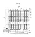
- FIG. 5 is a schematic diagram showing a configuration of the organic EL display device in the present embodiment.
- FIG. 6 is a circuit diagram for a pixel unit in the present embodiment
- FIG. 7 is a timing chart showing operations of the pixel unit in the embodiment of the present invention.
- FIG. 8 is a diagram for describing the operation in a Vth detection period T 11 of a pixel unit in the embodiment of the present invention.
- FIG. 9 is a diagram for describing the voltage held by a holding capacitor after the Vth detection
- FIG. 10 is a diagram for describing the operation in a write period T 12 of a pixel unit in the embodiment of the present invention.
- FIG. 11 is a diagram for describing the operation in a light-emission period T 13 of a pixel unit in the embodiment of the present invention.
- FIG. 12 is a diagram for describing results of Vth compensation in the embodiment of the present invention.
- FIG. 13 is a diagram showing a configuration of a luminance measurement system at the time of luminance measurement of the display panel
- FIG. 14 is a diagram showing an example of a correction parameter table held by a storage unit in the present embodiment
- FIG. 15 is a diagram showing an example of a function configuration diagram for a control unit in the present embodiment.
- FIG. 16 is a diagram showing voltage-luminance characteristics of a predetermined pixel unit and representative voltage-luminance characteristics
- FIG. 17 is a diagram for describing the representative voltage-luminance characteristics, a high gradation region, and a low gradation region in the present embodiment
- FIG. 18 is a flowchart showing an example of operations for calculating the correction parameter in the luminance measurement system in the present embodiment
- FIG. 19 is a diagram for describing a process by which a correction parameter calculation unit calculates the correction parameter in the present embodiment
- FIG. 20 is a flowchart showing an example of a process by which the correction parameter calculation unit calculates the correction parameter
- FIG. 21 is a diagram showing an effect of the correction parameter calculation process performed by the correction parameter calculation unit in the present embodiment.
- FIG. 22 is a diagram showing a configuration of a luminance measurement system at the time of luminance measurement of the display panel, according to a modification of the present embodiment
- FIG. 23 is a flowchart showing an example of operation by which a correction parameter determining device 200 determines the correction parameter, according to the modification of the present embodiment.
- FIG. 24 is a diagram for describing effects of the organic EL display device and the manufacturing method thereof according to the present invention.
- An organic electroluminescence (EL) display device includes: a display panel including pixel units each of which includes a light-emitting element, a drive element which is voltage-driven and controls supply of current to the light-emitting element, and a capacitor having a first electrode connected to a gate electrode of the drive element and a second electrode connected to one of a source electrode and a drain electrode of the drive element; a storage unit configured to store, for each of the pixel units, a correction parameter for correcting, in accordance with characteristics of the pixel unit, an image signal inputted from an external source; and a control unit configured to obtain, for each of the pixel units, a corrected signal voltage by reading, from the storage unit, the correction parameter corresponding to the pixel unit and multiplying the image signal corresponding to the pixel unit by the read correction parameter, wherein the control unit is configured (i) to cause, with each writing of the corrected signal voltage to a corresponding one of the pixel units, the capacitor included in the corresponding one of the pixel units
- luminance measurement for each pixel is performed only once on one gradation level belonging to a high gradation region of the representative voltage-luminance characteristics, and a correction parameter for matching the luminance at the one gradation level belonging to the high gradation region of the representative voltage-luminance characteristics is calculated from this one-time luminance measurement. Then, the image signal inputted from the external source is corrected by multiplying the image signal by the correction parameter, and a corrected signal voltage which corresponds to the corrected image signal is applied to the respective pixel units. Furthermore, a circuit for compensating the threshold voltage of a drive element is configured in each of the pixel units included in the display panel of the organic EL display apparatus.
- the corrected signal voltage is supplied to the capacitor in the state where the capacitor is holding the corresponding-voltage that corresponds to the threshold voltage of the drive element. Subsequently, current is caused to flow to the light-emitting element by supplying, between the gate and source electrodes of the drive element, a predetermined signal voltage obtained by adding the corrected signal voltage to the aforementioned corresponding-voltage.
- the drive current of the drive element which flows to the light-emitting element becomes a current corresponding to a voltage obtained by subtracting the threshold voltage of the drive element from the predetermined signal voltage. As such, it is possible to suppress variation of threshold voltage among drive elements included in the respective pixel units.
- the correction parameter can be calculated by merely performing the luminance measurement for one gradation level belonging to the high gradation region of the representative voltage-luminance characteristics, for the luminance measurement for the respective pixel units, in the manufacturing process of the organic EL display device, it is possible to significantly shorten the measurement tact from when luminance measurement for the respective pixel units is performed up to when the correction parameter is calculated, as compared to the conventional least-square method.
- the threshold voltage of the drive element is corrected in the pixel unit while the image signal is corrected using the correction parameter, and thus, together with being able to correct initial mobility and threshold voltage of the drive element, it is possible to correct even the deterioration over time of the threshold voltage of the drive element.
- a voltage is calculated, the voltage being a voltage such that the luminance emitted when the subject pixel unit is caused to emit light according to the corresponding-signal voltage is the standard luminance, and the correction parameter is a gain indicating a ratio between the corresponding-signal voltage and the calculated voltage.
- the correction parameter is a gain indicating a ratio between the luminance when the subject pixel is caused to emit light according to the corresponding signal voltage and the standard luminance.
- the second electrode of the capacitor is connected to the source electrode of the drive element
- each of the pixel units further includes: a first power line for determining a potential of the drain electrode of the drive element; a second power line connected to a second electrode of the light-emitting element; a third power line for supplying a first standard voltage which defines a voltage value of the first electrode of the capacitor; a data line for supplying a signal voltage; a first switching element which has one of terminals connected to the data line and the other of the terminals connected to the first electrode of the capacitor, and which switches between conduction and non-conduction between the data line and the first electrode of the capacitor; a second switching element which has one of terminals connected to the third power line and the other of the terminals connected to the first electrode of the capacitor, and which switches between conduction and non-conduction between the third power line and the first electrode of the capacitor; a third switching element which has one of terminals connected to the source electrode of the drive element and the other of
- the capacitor it is possible to cause the capacitor to hold the corresponding-voltage that corresponds to the threshold voltage of the drive circuit.
- control unit is configured (i) to cause a predetermined signal voltage to be generated in the first electrode of the capacitor, by supplying the corrected signal voltage to the capacitor by placing the first switching element in the ON state in the state where the capacitor is holding the corresponding-voltage, the predetermined signal voltage being obtained by adding, to the corresponding-voltage, a voltage obtained when a voltage value of the corrected signal voltage is divided in accordance with a ratio between a capacitance of the capacitor and a capacitance of the second capacitor, and (ii) to subsequently cause the current to flow to the light-emitting element by supplying the predetermined signal voltage between the gate electrode and the source electrode of the drive element by placing the third switching element in the ON state after placing the first switching element in the OFF state.
- the present aspect it is possible to cause, in the first electrode of the capacitor, the generation of a predetermined signal voltage obtained by adding, to the corresponding-voltage, a voltage obtained by dividing the voltage value of the corrected signal voltage according to the ratio of the capacitance of the capacitor and the capacitance of the second capacitor. Subsequently, current is caused to flow to the light-emitting element by supplying the predetermined signal voltage between the gate electrode and source electrode of the drive element.
- the drive current that is provided by the drive element to the light-emitting element is a current corresponding to a voltage obtained by subtracting the threshold voltage of the drive element from the potential difference between the gate electrode and the source electrode of the drive element. Therefore, in this case, by providing the predetermined signal voltage between the gate electrode and the source electrode of the drive element, the drive current provided to the light-emitting element becomes a current that corresponds to a voltage obtained by subtracting the threshold voltage of the drive element from the predetermined signal voltage. As a result, variation of threshold voltage among drive elements included in the respective pixel units can be suppressed, and thus correction precision in the low gradation region of the representative voltage-luminance characteristics can be enhanced.
- a voltage value of the first standard voltage is set in advance so that a potential difference between a first electrode and a second electrode of the light-emitting element when the first standard voltage is applied to the first electrode of the capacitor is a voltage lower than a threshold voltage of the light-emitting element at which the light-emitting element starts to emit light.
- the voltage value of the first standard voltage is set so that the light-emitting element does not emit light when the first standard voltage (a fixed voltage) is applied to the first electrode of the capacitor.
- the corresponding-voltage that corresponds to the threshold voltage is a voltage such that current is smaller than a current which flows when the threshold voltage is applied to the gate electrode of the drive element.
- a voltage for which current is smaller than the current which flows when the threshold voltage is applied to the gate of the drive element is added to the corrected signal voltage, and thus correction precision in the low gradation region of the representative voltage-luminance characteristics can be enhanced.
- the corresponding-voltage that corresponds to the threshold voltage is a voltage having a voltage value that is proportional to a voltage value of the threshold voltage and smaller than the voltage value of the threshold voltage.
- the corresponding-voltage that corresponds to the threshold voltage is a voltage having a voltage value that is proportional to the voltage value of the threshold voltage and is smaller than the voltage value of the threshold voltage.
- the voltage that the capacitor is holding is not the threshold voltage value itself but a voltage value that is smaller than the value of the threshold voltage.
- the low gradation region of the representative voltage-luminance characteristics corresponds to a voltage region that is smaller than the threshold voltage. With this, a value smaller than the voltage value of the threshold voltage is added to the corrected signal voltage, and thus the correction precision in the low gradation region of the representative voltage-luminance characteristics can be enhanced.
- the corresponding-signal voltage that corresponds to the single gradation level belonging to the high gradation region of the representative voltage-luminance characteristics is a voltage corresponding to a gradation level that is 20% to 100% of a maximum gradation level that can be displayed by each of the pixel units.
- a voltage corresponding to a gradation level that is 20% to 100% of the maximum gradation level is applied as the signal voltage corresponding to one gradation level belonging to the high gradation region of the representative voltage-luminance characteristics.
- the corresponding-signal voltage that corresponds to the single gradation level belonging to the high gradation region of the representative voltage-luminance characteristics is a voltage corresponding to a gradation level that is 30% of a maximum gradation level that can be displayed by each of the pixel units.
- a voltage corresponding to a gradation level that is 30% of the maximum gradation level is applied as the signal voltage corresponding to one gradation level belonging to the high gradation region of the representative voltage-luminance characteristics. This case allows for maximum suppression of correction error in the high gradation region.
- a corresponding-signal voltage that corresponds to a single gradation level belonging to an intermediate gradation region of the representative voltage-luminance characteristics is a voltage corresponding to a gradation level that is 10% to 20% of a maximum gradation level that can be displayed by each of the pixel units.
- a voltage corresponding to one gradation level belonging to a gradation region that is 10% to 20% of the maximum gradation level is applied as the signal voltage corresponding to one gradation level belonging to the high gradation region of the representative voltage-luminance characteristics.
- the representative voltage-luminance characteristics are voltage-luminescence characteristics of a single pixel unit among the pixel units included in the display panel.
- the representative voltage-luminance characteristics can be set as the voltage-luminance characteristics of a single arbitrary pixel unit among the pixel units included in the display panel.
- the representative voltage-luminance characteristics are characteristics obtained by averaging voltage-luminescence characteristics of two or more pixel units among the pixel units included in the display panel.
- the representative voltage-luminance characteristics are set in common throughout the entire display panel including the pixels, and can be calculated by averaging the voltage-luminance characteristics of the respective pixels included in the display panel.
- the display panel is divided into segments, and the representative voltage-luminance characteristics are set for each of the segments, the representative voltage-luminance characteristics being common among the pixels included in each of the segments, and in the calculating, the correction parameter with which the luminance emitted when the subject pixel is caused to emit light according to the predetermined signal voltage becomes a standard luminance is calculated for the subject pixel, the standard luminance being obtained when the predetermined signal voltage is inputted to the function of the representative voltage-luminance characteristics for the segment including the subject pixel unit.
- the display panel is divided into segments, and representative voltage-luminance characteristics common among the pixels included in each of the segments are set on a per segment basis. Subsequently, the correction parameter is calculated so that the luminance when a pixel is caused to emit light according to the predetermined signal voltage becomes the luminance obtained when the predetermined signal voltage is inputted to the function of the representative voltage-luminance characteristics for the segment including the pixel.
- the measuring device is an image sensor.
- the storage unit is configured to store only a gain out of the gain and offset which are correction parameters for correcting in accordance with characteristics of each of the pixel units.
- a method of manufacturing an organic electroluminescence (EL) display device includes: obtaining a function of representative voltage-luminance characteristics common throughout a display panel including pixel units each of which includes a light-emitting element, a drive element which is voltage-driven and controls supply of current to the light-emitting element, and a capacitor having a first electrode connected to a gate electrode of the drive element and a second electrode connected to one of a source electrode and a drain electrode of the drive element; causing the capacitor included in a subject pixel unit to hold a corresponding-voltage that corresponds to the threshold voltage of the drive element, the subject pixel unit being a current pixel unit to be processed among the pixel units included in the display panel; applying, to the drive element included in the subject pixel unit, a corresponding-signal voltage that corresponds to a single gradation level belonging to a high gradation region of the representative voltage-luminance characteristics, in the state where the capacitor is holding the corresponding-voltage, and measuring, using a
- FIG. 4 is a block diagram showing a configuration of an organic EL display device in an embodiment of the present invention.
- An organic EL display device 100 shown in FIG. 4 is a device which displays images using light-emitting elements, and includes a control unit 101 and a display panel 106 .
- the display panel 106 includes a display unit 105 , a scanning line drive circuit 103 , and a data line drive circuit 104 , and displays images on the display unit 105 based on signals inputted to the scanning line drive circuit 103 and the data line drive circuit 104 from the control unit 101 .
- the display unit 105 includes pixel units 40 (not shown) which are arranged in a matrix.
- a Vth compensation circuit which compensates (suppresses) the variation in the threshold voltage Vth of the TFT included in the pixel unit 40 is configured in each of the pixel units 40 .
- the control unit 101 includes a storage unit 102 , controls image signals for displaying on the display panel 106 , and causes the display panel 106 to display images.
- the control unit 101 reads a correction parameter (gain) corresponding to each of the pixel units 40 , and obtains a corrected signal voltage by multiplying or dividing the image signal corresponding to each of the pixel units 40 by the read correction parameter (gain). It should be noted that the control unit 101 shall be described in detail later.
- the storage unit 102 stores, for the respective pixel units 40 , the correction parameters (gain) for correcting the image signal inputted from an external source in accordance with the characteristics of the respective pixel units 40 .
- FIG. 5 is a schematic diagram showing a configuration of the organic EL display device in the present embodiment.
- the organic EL display device 100 includes the pixel units 40 which are arranged in, for example, a n ⁇ m matrix, the scanning line drive circuit 103 , the data line drive circuit 104 , and a power line drive circuit 108 .
- the scanning line drive circuit 103 supplies the pixel units 40 with a scanning signal Scn, a reset signal Rst, a merge signal Mrg, and a detection trigger signal Trg.
- the power line drive circuit 108 supplies power to the pixel units 40 .
- the scanning line drive circuit 103 supplies the scanning signal Scn to each of the pixel units 40 arranged in the row direction in FIG. 5 , via the scanning line 51 connected in common to such pixel units 40 .
- the scanning line drive circuit 103 supplies the reset signal Rst to each of the pixel units 40 arranged in the row direction via a reset line 52 connected in common to such pixel units 40 .
- the scanning line drive circuit 103 supplies the merge signal Mrg to each of the pixel units 40 arranged in the row direction via a merge line 53 connected in common to such pixel units 40 .
- the scanning line drive circuit 103 supplies the detection trigger signal Trg to each of the pixel units 40 arranged in the row direction via a detection trigger line 54 connected in common to such pixel units 40 .
- the data line drive circuit 104 supplies a data signal Data (signal voltage) to each of the pixel units 40 arranged in the column direction in FIG. 5 via a data line 20 connected in common to such pixel units 40 .
- Data signal voltage
- the scanning lines 51 , the reset lines 52 , the merge lines 53 , and the detection trigger lines 54 are n lines in number
- the data lines 20 are m lines in number.
- the power line drive circuit 108 supplies power to a high-voltage-side power line 24 and a low-voltage-side power line 25 which are connected in common to all of the pixel units 40 . Furthermore, the power line drive circuit 108 supplies a standard voltage (reference voltage) to a standard-voltage power line 56 connected in common to all the pixel units 40 .
- FIG. 6 is a circuit diagram for a pixel unit in the present embodiment.
- the pixel unit 40 shown in FIG. 6 is one pixel included in the display unit 105 and has a function of emitting light according to the signal voltage (data signal Data) supplied via the data line 20 . Furthermore, a Vth compensation circuit, which compensates (suppresses) the variation in the threshold voltage Vth of the TFT characteristics, is configured in each of the pixel units 40 .
- the pixel unit 40 includes an organic EL element D 1 , a drive transistor Q 1 , a holding capacitor C 1 , a switching transistor Q 2 which is a write switch, a reference transistor Q 3 , a isolation transistor Q 5 , and a detection trigger capacitor C 2 .
- the data line 20 for supplying signal voltage
- the high-voltage-side power line 24 for determining the potential of a drain electrode of the drive transistor Q 1
- the low-voltage-side power line 25 which is connected to a second electrode of the organic EL element D 1
- the scanning line 51 the reset line 52
- the merge line 53 the detection trigger line 54
- the standard-voltage power line 56 for supplying a first standard voltage which defines the voltage value of a first electrode of the holding capacitor C 1 .
- the organic EL element D 1 functions as a light-emitting element, and emits light according to the drive current of the drive transistor Q 1 .
- the organic EL element D 1 has a cathode (second electrode) connected to the low-voltage-side power line 25 , and an anode (first electrode) connected to a source (source electrode) of the drive transistor Q 1 .
- the voltage supplied by the low-voltage-side power line 25 is denoted by Vs, and is for example 0 (v).
- the drive transistor Q 1 is a voltage-driven drive element which controls the supply of current to the organic EL element D 1 , and causes the organic EL element D 1 to emit light by supplying current to the organic EL element D 1 .
- the drive transistor Q 1 has a gate (gate electrode) connected to the data line 20 via the switching transistor Q 2 , a source (source electrode) connected to an anode (first electrode) of the organic EL element D 1 , and a drain (drain electrode) connected to the high-voltage-side power line 24 .
- Vdd the voltage supplied to the high-voltage-side power line 24 is denoted as Vdd, and is, for example, 20 (v).
- the drive transistor Q 1 converts the signal voltage (data signal Data) supplied to its gate into a signal current corresponding to the signal voltage (data signal Data), and supplies the signal current obtained from the conversion to the organic EL element D 1 .
- the holding capacitor C 1 holds the voltage which determines the amount of current to be supplied by the drive transistor Q 1 .
- the holding capacitor C 1 is connected between the source (low-voltage-side power line 25 ) of the drive transistor Q 1 and the gate of the drive transistor Q 1 .
- the holding capacitor C 1 has a first electrode connected to the gate electrode of the drive transistor Q 1 and a second electrode connected to the source electrode of the drive transistor Q 1 .
- the holding capacitor C 1 has, for example, a function of maintaining the immediately preceding signal voltage and causing drive current to be continuously supplied from the drive transistor Q 1 to the organic EL element D 1 , even after the switching transistor Q 2 switches to the OFF state. It should be noted that, in actuality, the holding capacitor C 1 holds an electric charge obtained by multiplying a signal voltage by a capacitance.
- the switching transistor Q 2 which corresponds to the first switching element in the present invention, has one terminal connected to the data line 20 and the other terminal connected to the first electrode of the holding capacitor C 1 , and switches between conduction and non-conduction between the data line 20 and the holding capacitor C 1 .
- the switching transistor Q 2 has a function for writing, in the holding capacitor C 1 , a signal voltage (data signal Data) that is in accordance with the image signal (corrected signal voltage).
- the switching transistor Q 2 has a gate connected to the scanning line 51 , and one of a source and a drain connected to the data line 20 .
- the switching transistor Q 2 has a function of controlling the timing for supplying the signal voltage (data signal Data) of the data line 20 to the gate of the drive transistor Q 1 .
- the switching transistor Q 2 is a writing switch for writing, in the holding capacitor C 1 , a voltage that is in accordance with the image signal (corrected signal voltage).
- the reference transistor Q 3 which corresponds to the second switching element in the present invention, has one terminal connected to the standard-voltage power line 56 and the other terminal connected to the first electrode of the holding capacitor C 1 , and switches between conduction and non-conduction between the standard-voltage power line 56 and the holding capacitor C 1 .
- the reference transistor Q 3 has a function of providing a standard voltage (Vr) to the gate of the drive transistor Q 1 , during the detection of the threshold voltage Vth of the drive transistor Q 1 .
- the reference transistor Q 3 has one of a drain and a source connected to the gate of the drive transistor Q 1 , and the other of the drain and the source connected to the standard-voltage power line 56 for applying a reference voltage (Vr).
- the reference transistor Q 3 has a gate connected to the reset line 52 .
- the reference transistor Q 3 is a reference switch for providing a standard voltage (reference voltage) to the gate (gate electrode) of a drive transistor Q 1 , during the detection of threshold voltage Vth (or a corresponding-voltage that corresponds to the threshold voltage Vth) of the drive transistor Q 1 .
- the isolation transistor Q 5 which corresponds to the third switching element in the present invention, has one terminal connected to the source electrode of the drive transistor Q 1 and the other terminal connected to the second electrode of the holding capacitor C 1 , and switches between conduction and non-conduction between the source electrode of the drive transistor Q 1 and the second electrode of the holding capacitor C 1 .
- the isolation transistor Q 5 has a function of isolating the holding capacitor C 1 from the drive transistor Q 1 during a write period in which voltage is written into the holding capacitor C 1 .
- the isolation transistor Q 5 has one of a drain and a source connected to the source of the drive transistor Q 1 , and the other of the drain and the source connected to the second electrode of the holding capacitor C 1 .
- the isolation transistor Q 5 has a gate connected to the merge line 53 .
- the isolation transistor Q 5 is a isolation switch for isolating the holding capacitor C 1 from the source (source electrode) of the drive transistor Q 1 during a write period in which voltage is written into the holding capacitor C 1 .
- the detection trigger capacitor C 2 corresponds to the second capacitor in the present invention, and has a first electrode connected to the second electrode of the holding capacitor C 1 .
- the detection trigger capacitor C 2 has a first electrode connected to the second electrode of the holding capacitor C 1 , and the source of the drive transistor Q 1 is connected between the first electrode of the detection trigger capacitor C 2 and the second electrode of the holding capacitor C 1 .
- a second electrode of the detection trigger capacitor C 2 is connected to detection trigger line 54 .
- the detection trigger capacitor C 2 has a function of dividing the voltage to be applied to the first electrode of the holding capacitor C 1 .
- VData signal voltage
- VData a signal voltage
- VData a voltage resulting from the division of the signal voltage (VData) according to the ratio between the capacitances of the holding capacitor C 1 and the detection trigger capacitor C 2 is applied to the holding capacitor C 1 .
- the detection trigger line 54 which corresponds to the bias voltage line in the present invention, is connected to the second electrode of the detection trigger capacitor C 2 and causes, in the second electrode of the holding capacitor C 1 , the generation of a second standard voltage which is lower than a value obtained from subtracting the threshold voltage of the drive transistor Q 1 from the first standard voltage. Specifically, the detection trigger line 54 supplies a voltage for reducing a source voltage Vs of the drive transistor Q 1 , in order to detect the threshold voltage Vth (or the corresponding-voltage that corresponds to the threshold voltage Vth) of the drive transistor Q 1 .
- the pixel unit 40 is configured as described above.
- each of the drive transistor Q 1 , the switching transistor Q 2 , the reference transistor Q 3 , and the isolation transistor Q 5 included in the pixel unit 40 is, for example, an N-channel thin-film transistor or an enhancement transistor. Of course, these transistors may be channel thin-film transistors, or depression transistors.
- FIG. 7 is a timing chart showing the operations of a pixel unit in the embodiment of the present invention.
- the control unit 101 performs, in each of the pixel units 40 and within a certain measurement period, the operation for detecting the threshold voltage Vth of the drive transistor Q 1 , the operation for writing a signal voltage (data signal Data) corresponding to the image signal (corrected signal voltage) into the holding capacitor C 1 , and the operation for causing the organic EL element D 1 to emit light according to the voltage written into the holding capacitor C 1 .
- the period for detecting the threshold voltage Vth of the drive transistor Q 1 is a Vth detection period T 11
- the period for writing the signal voltage (data signal Data) corresponding to the image signal (corrected signal voltage) into the holding capacitor C 1 is a write period T 12
- the period for causing the organic EL element D 1 to emit light based on the voltage written into the holding capacitor C 1 is a light-emission period T 13 .
- the Vth detection period T 11 , the write period T 12 , and the light-emission period T 13 are defined for each of the pixel units 40 , and the phases of the aforementioned three periods need not match for all the pixel units 40 .
- FIG. 8 is a diagram for describing the operation in the Vth detection period T 11 of a pixel unit in the embodiment of the present invention. It should be noted that, for the sake of description, the switching transistor Q 2 , the reference transistor Q 3 , and the isolation transistor Q 5 in FIG. 6 are replaced in FIG. 8 by a switch SW 2 , a reference switch SW 3 , and a isolation switch SW 5 , respectively. Furthermore, the organic EL element D 1 is replaced by a capacitor CE.
- a merge signal Mrg supplied to the merge line 53 is set to a high level so as to place the isolation switch SW 5 (isolation transistor Q 5 ) into the ON state.
- a reset signal Rst supplied to the reset line 52 is at the low level, and thus the reference switch SW 3 (reference transistor Q 3 ) is in the ON state.
- the reset signal Rst is set to the high level so as to place the reference switch SW 3 into the ON state.
- the standard voltage Vr (here, 0 V) is applied to the gate of the drive transistor Q 1 via the reference switch SW 3 , and thus the drive transistor Q 1 is turned ON. Therefore, current does not flow to the organic EL element D 1 , and the organic EL element D 1 functions as the capacitor CE. Furthermore, the source voltage Vs of the drive transistor Q 1 becomes an OFF voltage VEoff of the organic EL element D 1 .
- the voltage value of the standard voltage Vr is not limited to 0 V. It is sufficient that the voltage value of the standard voltage Vr be set in advance so that, when the standard voltage Vr is applied to the first electrode of the holding capacitor C 1 , the potential difference between the first electrode and second electrode of the organic EL element D 1 is a voltage that is lower than the threshold voltage of the organic EL element D 1 at which the organic EL element D 1 starts to emit light. Setting in this manner is done because it can prevent the organic EL element D 1 from emitting light, and it can keep the drive transistor Q 1 in the reset state.
- the detection trigger signal Trg is lowered by as much as the voltage ⁇ V.
- the source voltage Vs of the drive transistor Q 1 drops by as much as the voltage obtained by dividing the voltage ⁇ V using the capacitance of the detection trigger capacitor C 2 and the combined capacitance of the holding capacitor C 1 and the capacitor CE.
- the source voltage Vs is as shown in (Equation 1)
- Vs VE off ⁇ ( C 2/( C 1+ C 2+ CE )) ⁇ V (Equation 1)
- the gate-source voltage Vgs of the drive transistor Q 1 becomes equal to or greater than the threshold voltage Vth, and thus the drive transistor Q 1 turns ON.
- the control unit 101 causes a first standard voltage Vr to be applied to the first electrode of the holding capacitor C 1 by turning ON the reference transistor Q 3 in a state where the isolation transistor Q 5 is turned ON after turning OFF the switching transistor Q 2 , and causes a potential difference that is greater than the threshold voltage of the drive transistor Q 1 to be generated in the holding capacitor C 1 by applying a second standard voltage ( ⁇ V) to the second electrode of the detection trigger capacitor C 2 .
- the drive transistor Q 1 turns ON, the electric charges of the holding capacitor C 1 and the capacitor CE are discharged together with the charging of the detection trigger capacitor C 2 , and the source voltage Vs begins to rise.
- the drive transistor Q 1 turns OFF at the point in time when the gate-source voltage Vgs and the threshold voltage Vth (or the corresponding-voltage that corresponds to the threshold voltage Vth) of the drive transistor Q 1 become equal.
- the source voltage Vs of the drive transistor Q 1 is as shown in (Equation 2), and the voltage VC 1 of the holding capacitor C 1 becomes equal to the threshold voltage Vth.
- Vs ⁇ Vth (Equation 2)
- the threshold voltage Vth (or the corresponding-voltage that corresponds to the threshold voltage Vth) is held in the holding capacitor C 1 , the detection capacitor C 2 , and the capacitor CE.
- the control unit 101 performs a Vth compensation operation in which the voltage held by the holding capacitor C 1 becomes the threshold voltage Vth (or the corresponding-voltage that corresponds to the threshold voltage Vth). More specifically, after allowing the passage of time up to when the potential difference between the first electrode and second electrode of the holding capacitor C 1 reaches the threshold voltage of the drive transistor Q 1 and the drive transistor Q 1 turns OFF, the control unit 101 performs a Vth compensation operation to cause the corresponding-voltage that corresponds to the threshold voltage of the drive transistor Q 1 to be held in the holding capacitor C 1 by turning OFF the reference transistor Q 3 and the isolation transistor Q 5 .
- the merge signal Mrg is set to the low level so as to place the isolation switch SW 5 (isolation transistor Q 5 ) into the OFF state.
- the reset signal Rst is set to the low level so as to place the reference switch SW 3 into the OFF state.
- the scanning signal Scn supplied to the scanning line 51 is at the low level, and the switch SW 2 (switching transistor Q 2 ) is in the OFF state.
- threshold voltage Vth is synonymous to the corresponding-voltage that corresponds to the threshold voltage Vth, and such corresponding-voltage is ideally equal to the threshold voltage Vth and is normally a value smaller than the threshold voltage Vth.
- the reason why the voltage held by the holding capacitor C 1 is a voltage corresponding to a voltage that is normally lower than Vth in the Vth compensation operation shall be described.
- FIG. 9 is a diagram for describing the voltage held by the holding capacitor after Vth detection.
- (a) in FIG. 9 is a graph selectively illustrating the drive transistor Q 1 and the holding capacitor C 1 .
- illustration of the isolation transistor Q 5 is omitted since the isolation transistor Q 5 is turned ON during the Vth detection period. Since the voltage applied to the holding capacitor C 1 is the gate-source voltage of the drive transistor Q 1 , it shall be described as Vgs.
- a voltage (VA) that is higher than the threshold voltage Vth of the drive transistor Q 1 is applied to the holding capacitor C 1 shown in (a) in FIG. 9 .
- the holding capacitor C 1 discharges the held electric charge to the Vdd-side through the TFT channel of the drive transistor Q 1 .
- the current flowing in the TFT channel of the drive transistor Q 1 smaller when the potential between the electrodes of the holding capacitor C 1 becomes small, that is, when the voltage Vgs applied to the holding capacitor C 1 becomes small, the discharging takes time.
- the voltage held by the holding capacitor C 1 has a voltage value that is proportional to the voltage value of the threshold voltage Vth and smaller than the voltage value of the threshold voltage Vth.
- the corresponding-voltage that corresponds to the threshold voltage is a gate voltage for which current is smaller than the current which flows between the source and drain when the signal voltage for which the threshold voltage has been compensated is applied to the gate of the drive transistor Q 1 .
- the drive transistor Q 1 is, for example, an enhancement N-channel thin-film transistor and the corresponding-voltage that corresponds to the threshold voltage normally has a value that is smaller than the threshold voltage Vth in the above description, they are not limited to such.
- the drive transistor Q 1 may be, for example, a depression N-channel thin-film transistor, or it may be an enhancement P-channel thin-film transistor or a depression P-channel thin-film transistor.
- the voltage held by the holding capacitor C 1 has a voltage value that becomes bigger in the minus-side than the voltage value of the threshold voltage Vth, and thus although the numerical value itself becomes smaller, the absolute value of the voltage becomes bigger.
- the voltage held by the holding capacitor C 1 has a voltage value that is closer to the plus-side than the voltage value of the threshold voltage Vth, and thus, although the value, as an absolute value, becomes smaller, the numerical value itself becomes bigger.
- the above described corresponding-voltage that corresponds to the threshold voltage is the gate voltage for which current becomes smaller than the current which flows when the threshold voltage is applied to the gate of the drive transistor Q 1 .
- FIG. 10 is a diagram for describing the operation in the write period T 12 of a pixel unit in the embodiment of the present invention.
- the scanning signal Scn is set to the high level so as to place the switch SW 2 into the ON state. Then, signal voltage Vdata corresponding to the image signal (corrected signal voltage) supplied to the data line 20 at this time is applied to the drive transistor Q 1 .
- the control unit 101 supplies the image signal to the data line 20 as described above, such image signal is a corrected signal voltage obtained by multiplying or dividing the image signal by the correction parameter in the storage unit 102 .
- the voltage VC 1 of the holding capacitor C 1 increases by as much as the voltage obtained by dividing the capacitance of the signal voltage Vdata between the holding capacitor C 1 and the detection trigger capacitor C 2 , and becomes as shown in (Equation 3).
- the voltage VC 1 applied to the holding capacitor C 1 assumes a magnitude that is equal to or greater than the threshold voltage Vth of the drive transistor Q 1 .
- the control unit 101 supplies the corrected signal voltage to the holding capacitor C 1 by turning ON the switching transistor Q 2 in a state where the holding capacitor C 1 is holding the corresponding-voltage that corresponds to the threshold voltage.
- the control unit 101 causes, in the first electrode of the holding capacitor C 1 , the generation of a predetermined signal voltage which is obtained by adding, to the corresponding-voltage that corresponds to the threshold voltage, the voltage obtained by dividing the voltage value of the corrected signal voltage according to the ratio of the capacitance of the holding capacitor C 1 and the capacitance of the detection trigger capacitor C 2 .
- VC 1 Vth +( C 2/( C 1 +C 2)) ⁇ V data (Equation 3)
- the scanning signal Scn is returned to the low level so as to place the switch SW 2 into the OFF state.
- the detection trigger signal Trg is returned to the original voltage.
- control unit 101 performs the write operation of starting the supply of the image signal (corrected signal voltage) to the first electrode of the holding capacitor C 1 by turning ON the switching transistor Q 2 while the reference transistor Q 3 is kept OFF, in the state where the holding capacitor C 1 is holding the corresponding-voltage that corresponds to the threshold voltage Vth.
- FIG. 11 is a diagram for describing the operation in the light-emission period T 13 of a pixel unit in the embodiment of the present invention.
- a merge signal Mrg is set to the high level so as to place the isolation switch SW 5 (isolation transistor Q 5 ) into the ON state.
- the scanning signal Scn supplied to the scanning line 51 is at the low level, and the switch SW 2 (switching transistor Q 2 ) is in the OFF state.
- the reset signal Rst supplied to the reset line 52 is at the low level, and the reference switch SW 3 (reference transistor Q 3 ) is in the OFF state.
- the voltage VC 1 of the holding capacitor C 1 becomes the gate-source voltage Vgs of the drive transistor Q 1 .
- a voltage that is equal to or greater than the threshold voltage Vth and is a voltage (corresponding-voltage) that corresponds to the threshold voltage Vth is stored as the voltage VC 1 , and thus a current that is in accordance with the signal voltage Vdata corresponding to the image signal flows in the drive transistor Q 1 , and the organic EL element D 1 is caused to emit light at a luminance that is in accordance with the image signal.
- the control unit 101 supplies a predetermined signal voltage obtained from the corresponding-voltage and the corrected signal voltage, between the gate electrode and the source electrode of the drive transistor Q 1 , and provides current to the organic EL element D 1 .
- the current Ipx 1 flowing to the organic EL element D 1 at this time is as shown in (Equation 4), and is not affected by the threshold voltage Vth (or the corresponding-voltage that corresponds to the threshold voltage Vth).
- ⁇ is a coefficient that is determined depending on the mobility ⁇ of the drive transistor Q 1 , a gate insulation film capacitance Cox, a channel length L, and a channel width W, and is as shown in (Equation 5).
- ⁇ ⁇ Cox ⁇ ( W/L ) (Equation 5)
- the isolation switch SW 5 that is, the isolation transistor Q 5 is placed into the ON state before hand in the light-emission period T 13 , the threshold voltage of the isolation transistor Q 5 changes and ON characteristics deteriorate.
- the merge signal Mrg be set at the low level and the switch SW 5 be set in the OFF state in a time t 42 in which the source potential of the drive transistor Q 1 is sufficiently charged at the connection node between the holding capacitor C 1 and the detection trigger capacitor C 2 . It should be noted that, even when the switch SW 5 is placed in the OFF state, the voltage of the respective units does not change, and thus there is no effect on the light-emission by the organic EL element D 1 .
- the control unit 101 causes the holding capacitor C 1 included in the respective pixel units 40 to detect the threshold voltage of the drive transistor Q 1 ; then after the detection of the threshold voltage, causes the holding capacitor C 1 to hold the corresponding-voltage that corresponds to the threshold voltage of the drive transistor Q 1 ; supplies the corrected signal voltage to the holding capacitor C 1 in the state where the holding capacitor C 1 is holding the corresponding-voltage; and causes the organic EL element D 1 to emit light by causing current to flow to the organic EL element D 1 by supplying, between the gate and source electrodes of the drive transistor Q 1 , a predetermined signal voltage obtained by adding to or subtracting from the corresponding-voltage the corrected signal voltage.
- the drive current that is provided by the drive transistor Q 1 to the organic EL element D 1 is a current corresponding to a voltage obtained by subtracting the threshold voltage of the drive transistor Q 1 from the potential difference between the gate electrode and the source electrode of the drive transistor Q 1 . Therefore, by supplying the predetermined signal voltage between the gate electrode and the source electrode of the drive transistor Q 1 , the current flowing to the organic EL element D 1 becomes a current corresponding to a voltage obtained by subtracting the threshold voltage of the drive transistor Q 1 from the predetermined signal voltage. As a result, it is possible to perform the Vth compensation for suppressing variation of threshold voltages between the drive transistors Q 1 included in the respective pixel units 40 .
- the term for the threshold voltage Vth is not included in the current Ipx 1 flowing to the organic EL element D 1 . Therefore, even when the threshold voltage Vth of the drive transistor Q 1 fluctuates according to change over time, the current Ipx 1 flowing to the organic EL element D 1 is not affected and it is possible to cause the organic EL element D 1 to emit light at a luminance corresponding to the image signal.
- the Vth compensation circuit is configured in the pixel unit 40 .
- the luminance of the organic EL element D 1 is determined according to the voltage of the holding capacitor C 1 , it is necessary to perform driving such that the voltage of the holding capacitor C 1 does not cause unexpected fluctuation. As such, by controlling the respective transistors based on the sequence shown in FIG. 7 , it is possible to reliably control the voltage of the holding capacitor C 1 .
- Vth compensation is performed for each of the pixel units 40 through the Vth compensation circuit configured in each of the pixel units 40 .
- FIG. 12 is a diagram for describing results of the Vth compensation in the embodiment of the present invention.
- (a) in FIG. 12 is a graph showing the voltage-luminance characteristics of pixel units 40 when Vth compensation is not performed
- (b) in FIG. 12 is a graph showing the voltage-luminance characteristics of pixel units 40 after Vth compensation.
- FIG. 12 illustrates, for example, four pixel units 40 (A to D).
- the threshold voltage Vth in the TFT included in the respective pixel units 40 there are variations in the threshold voltage Vth in the TFT included in the respective pixel units 40 .
- Vth compensation is performed by the Vth compensation circuit configured in each of the pixel units 40
- the voltage-luminance characteristics of the pixel units 40 in A to D are uniform for the luminance in the low gradation region. This is the same even when the threshold voltage Vth fluctuates due to change over time.
- Vth compensation is performed for the respective pixel units 40 with the writing of a corresponding image signal (compensated signal voltage) into the respective pixel units 40 by the control unit 101 .
- Vth compensation functions as an offset for correcting, to a predetermined standard luminance, the luminance of the organic EL element D 1 corresponding to the image signal supplied to the respective pixel units 40 .
- a correction parameter (gain) is stored in advance in the storage unit 102 included in the control unit 101 .
- the luminance measurement for each pixel is performed in order to obtain the correction parameter (gain) to be stored in advance in the storage unit 102 , that is, the correction parameter (gain) for correcting, to a predetermined standard luminance, the luminance of the organic EL element D 1 which corresponds to the image signal supplied to the respective pixel units 40 .
- offset is not obtained as a correction parameter because this is compensated in the Vth compensation.
- FIG. 13 is a diagram showing a configuration of a luminance measurement system at the time of luminance measurement for a display panel.
- Luminance measurement for the display panel 106 is performed on the display panel 106 of the organic EL display device 100 , by using a measuring device 210 .
- the luminance unevenness in the display panel 106 can be reduced while shortening the luminance measurement time, as described later.
- the luminance measurement system shown in FIG. 13 includes the organic EL display device 100 , a correction parameter determining device 200 , and the measuring device 210 , and is intended to perform luminance measurement on the display panel 106 of the organic EL display device 100 and obtain gain which is the correction parameter.
- the organic EL display device 100 includes the control unit 101 and the display panel 106 .
- the display panel 106 includes the display unit 105 , the scanning line drive circuit 103 , and the data line drive circuit 104 , and displays images on the display unit 105 based on signals inputted to the scanning line drive circuit 103 and the data line drive circuit 104 from the control unit 101 .
- the control unit 101 includes the storage unit 102 and a control circuit 107 , and has a function of supplying image signals for displaying on the display panel 106 , and causing the display panel 106 to display images, by controlling the scanning line drive circuit 103 and the data line drive circuit 104 .
- the control unit 101 causes the pixel units 40 included in the display panel 106 to emit light, according to an instruction from a measurement control unit 201 .
- the control unit 101 further writes, into the storage unit 102 , the correction parameter (gain) for each of the pixel units 40 calculated by a correction parameter calculation unit 202 .
- FIG. 14 is a table showing an example of a correction parameter table held by the storage unit in the present embodiment.
- FIG. 15 is a diagram showing an example of a function configuration diagram for the control unit in the present embodiment.
- the storage unit 102 stores, for each of the pixel units 40 , the correction parameter (gain) for correcting the image signal inputted from an external source, in accordance with the characteristics of each of the pixel units 40 .
- the storage unit 102 stores a correction parameter table 102 a including the correction parameter (gain) for each of the pixel units 40 .
- the correction parameter table 102 a is a data table which includes the correction parameter (gain) for each of the pixel units 40 .
- the correction parameters (gain) are denoted by a 11 to amn, that is, the correction parameter table 102 a stores a correction parameter indicating gain for each of the pixel units 40 , in correspondence with the matrix of the display unit 105 (m rows ⁇ n columns).
- Vth compensation is also performed at the time of luminance measurement of the display panel 106 , and the correction parameter (gain) is calculated by performing luminance measurement of the display panel 106 in the Vth-compensated, that is, in the offset state.
- the control circuit 107 includes a pixel position detection unit 1071 , an image-to-luminance conversion unit 1072 , a luminance-to-voltage conversion unit 1073 , a multiplication unit 1074 , and a drive circuit timing controller 1075 .
- the pixel position detection unit 1071 detects, according to a synchronizing signal inputted simultaneously with the image signal inputted from the external source, the pixel position information of the image signal.
- the detected pixel position is x row and y column.
- the image-to-luminance conversion unit 1072 converts the image signal inputted from the external source into a luminance signal, and outputs the luminance signal to the luminance-to-voltage conversion unit 1073 .
- the image-to-luminance conversion unit 1072 has, for example, an image-to-luminance conversion LUT stored in a memory, and converts the image signal inputted from the external source into a luminance signal by reading the luminance signal corresponding to the image signal.
- the luminance-to-voltage conversion unit 1073 converts the luminance signal outputted from the image-to-luminance conversion unit 1072 into a voltage signal, and outputs the voltage signal to the multiplication unit 1074 .
- the luminance-to-voltage conversion unit 1073 reads, for example, from a representative LUT derived based on a representative conversion curve stored in a memory, the voltage signal of the x row and y column corresponding to the luminance signal outputted from the image-to-luminance conversion unit 1072 , and outputs the voltage signal to the multiplication unit 1074 .
- the multiplication unit 1074 corrects the voltage signal by multiplying the gain (here, the voltage gain) which is the correction parameter corresponding to each of the pixel units and which is stored in the storage unit 102 , with the voltage signal. Specifically, a voltage gain axy of the x row and y column and the voltage signal value of the x row and y column are multiplied, and a corrected voltage signal of the x row and y column is generated.
- the multiplication unit 1074 outputs the corrected voltage signal to the drive circuit timing controller 1075 .
- the multiplication unit 1074 may correct the voltage signal by calculation other than multiplication, such as dividing the voltage gain corresponding to each of the pixel units and which is stored in the storage unit 102 in advance, by the voltage signal outputted from the luminance-to-voltage conversion unit 1073 .
- the drive circuit timing controller 1075 outputs the converted voltage signal of the x row and y column to the data line drive circuit 104 .
- This voltage signal is converted to an analog voltage and inputted to the data line drive circuit 104 , or is converted into an analog voltage inside the data line drive circuit 104 . Subsequently, the analog voltage is supplied, as data voltage, from the data line drive circuit 104 to the respective pixels.
- control unit 101 reads the correction parameter (gain) corresponding to the respective pixel units 40 from the storage unit 102 , and obtains a corrected signal voltage by performing the calculation on the image signal corresponding to the respective pixel units 40 using the read correction parameter (gain).
- control unit 101 causes the display panel 106 to display an image by outputting the corrected signal voltage obtained by calculation to the display panel 106 .
- the measuring device 210 is a measuring device which can measure luminance that is emitted by the pixel units 40 included in the display panel 106 .
- the measuring device 210 is an image sensor such as a charge coupled device (CCD) image sensor, and can precisely measure the luminance of all the pixel units 40 included in the display unit 105 of the display panel 106 in one image-capturing operation.
- CCD charge coupled device
- the measurement unit 210 is not limited to an image sensor and may be any type of measuring device as long as it is capable of measuring the luminance of the pixel units 40 of the display unit 105 .
- the correction parameter determining device 200 includes the measurement control unit 201 and the correction parameter calculation unit 202 .
- the correction parameter determining device 200 is a device which determines the correction parameter (gain) for correcting, to the standard luminance, the luminance of the pixel units 40 included in the display unit 105 of the display panel 106 , based on the luminance of the respective pixel units 40 measured by the measuring device 210 .
- the correction parameter determining device 200 outputs the determined correction parameter (gain) to the control unit 101 of the organic EL display device 100 .
- the standard luminance is a luminance obtained when a predetermined voltage is inputted to the function of the representative voltage-luminance characteristics.
- the measurement control unit 201 is a processing unit which measures the luminance emitted by the pixel units 40 included in the display panel 106 .
- the measurement control unit 201 first obtains the function of the representative voltage-luminance characteristics that is common among the pixel units 40 included in the display panel 106 .
- the representative voltage-luminance characteristics are voltage-luminance characteristics that serve as a standard for making luminance uniform.
- the representative voltage-luminance characteristics are the voltage-luminance characteristics of a pixel unit 40 in a predetermined position among the pixel units 40 included in the display panel 106 .
- the representative voltage-luminance characteristics are voltage-luminance characteristics obtained by averaging the voltage-luminance characteristics of two or more pixel units 40 among the pixel units 40 included in the display panel 106 .
- the correction parameter is calculated so that the luminance of each of the pixel units 40 included in the display panel 106 assumes the representative voltage-luminance characteristics common throughout the entire display panel 106 , using such correction parameters to correct the image signals produces the effect of being able to even out the luminance of the lights emitted by the respective pixel units 40 .
- the function of the representative voltage-luminance characteristics is a function of the relationship between the signal voltage supplied to the drive transistor Q 1 and the luminance emitted by the pixel unit 40 by way of the organic EL element D 1 . It should be noted that the function of the representative voltage-luminance characteristics is assumed to be determined in advance through a separate measurement and the like.
- the measurement control unit 201 obtains the luminance by causing the control unit 101 to cause the pixel units 40 included in the display panel 106 to emit light, and causing the measuring device 210 to measure the luminance emitted by the pixel units 40 .
- the measurement control unit 201 obtains the luminance by applying, to the drive transistor Q 1 which is the drive element included in a pixel unit 40 , a signal voltage corresponding to one gradation level belonging to a high gradation region (or an intermediate gradation region) of the representative voltage-luminance characteristics, in the state where the holding capacitor C 1 included in the pixel unit 40 holds the corresponding-voltage that corresponds to the threshold voltage Vth (in the Vth-compensated state), and by measuring the luminance emitted by the pixel unit 40 , using the predetermined measuring device 210 .
- FIG. 16 shows the voltage-luminance characteristics of a predetermined pixel unit and the representative voltage-luminance characteristics.
- (a) in FIG. 16 shows the voltage-luminance characteristics of a predetermined pixel unit 40
- (b) in FIG. 16 shows voltage-luminance characteristics in the case of Vth compensation, that is, the case where the threshold voltage Vth of the drive transistor Q 1 is added as the offset, in the predetermined pixel unit 40 .
- the voltage-luminance characteristics of the predetermined pixel unit 40 and the representative voltage-luminance characteristics show close characteristics in the low gradation region of the representative voltage-luminance characteristics.
- the voltage-luminance characteristics of the pixel units 40 show a matching state with the representative voltage-luminance characteristics in the low gradation region.
- the voltage-luminance characteristics of the predetermined pixel unit 40 and the representative voltage-luminance characteristics do not show close characteristics. In other words, with the high gradation region of the representative voltage-luminance characteristics, there is a gap between both characteristics, and both show an unmatched state.
- the measurement control unit 201 measures a signal voltage corresponding to one gradation level belonging to either the intermediate gradation region or the high gradation region among the regions of the representative voltage-luminance characteristics, and calculates the gain. Specifically, calculating the gain in the high gradation region of the representative voltage-luminance characteristics is effective because, aside from characteristics becoming close in the low gradation region due to the Vth compensation, it is also possible to bring the characteristics close even in the high gradation region.
- the correction parameter calculation unit 202 calculates the correction parameter (gain) for a pixel, using the luminance obtained by the measurement control unit 201 and the function of the representative voltage-luminance characteristics.
- the correction parameter calculation unit 202 outputs the calculated correction parameter (gain) to the control unit 101 .
- the control unit 101 stores the correction parameter (gain) in the storage unit 102 .
- the correction parameter calculation unit 202 ( i ) obtains, by calculation, the voltage such that the luminance obtained by the measurement control unit 201 , that is, the luminance when the pixel unit 40 is caused to emit light according to the corresponding signal voltage is the luminance obtained when the corresponding signal voltage is inputted to the function of the representative voltage-luminance characteristics, and calculates the correction parameter (gain) indicating the ratio between such corresponding signal voltage and the voltage obtained by calculation.
- the corresponding signal voltage is the signal voltage applied to the drive transistor Q 1 included in the pixel unit 40 in the state where the holding capacitor C 1 included in the pixel unit 40 holds the above-described corresponding-voltage that corresponds to the threshold voltage Vth, and is the signal voltage corresponding to one gradation level belonging to the high gradation region of the representative voltage-luminance characteristics.
- the correction parameter (gain) is the ratio of the corresponding signal voltage to the voltage obtained in the case where the luminance when the pixel unit 40 is caused to emit light according to the corresponding signal voltage is inputted to the function of the representative voltage-luminance characteristics.
- correction parameter may be calculated as the ratio between the luminance when the pixel unit 40 is caused to emit light according to the corresponding signal voltage and the luminance (standard luminance) obtained when the corresponding signal voltage is inputted.
- the correction parameter calculation unit 202 obtains the correction parameter for the respective colors, namely, the red color, green color, and blue color emitted by the organic EL element D 1 .
- FIG. 17 is a diagram for describing the representative voltage-luminance characteristics, the high gradation region, and the low gradation region in the present embodiment.
- the pixel units 40 included in the display panel 106 have respectively different voltage-luminance characteristics.
- the representative voltage-luminance characteristics are assumed to be the voltage-luminance characteristics of a single arbitrary pixel among the pixel units 40 included in the display panel 106 . It should be noted that the representative voltage-luminance characteristics are the characteristics set in common throughout the entirety of the display panel 106 including the pixel units 40 , and may be the characteristics obtained by averaging the voltage-luminance characteristics of the respective pixel units 40 included in the display panel 106 .
- FIG. 17 shows the representative voltage-luminance characteristics that is in accordance with human visual sensitivity.
- the human eye has a sensitivity that is close to a LOG function
- representative voltage-luminance characteristics that are in accordance with human visual sensitivity show characteristics in which luminance is represented by the curve of the LOG function.
- the human eye since the human eye does not easily recognize luminance unevenness in the high gradation regions and easily recognizes luminance unevenness in the low gradation regions, in order to adjust to human visual sensitivity, it is preferable to set the width of the high gradation region wide and the width of the low gradation region narrow.
- the signal voltage corresponding to one gradation level belonging to the high gradation region of the representative voltage-luminance characteristics is preferably a voltage corresponding to one gradation level that is 20% to 100% of the maximum gradation level that can be displayed by each of the pixel units 40 , and is more preferably a voltage corresponding to one gradation level that is 30% of the maximum gradation level. This is because, this allows for maximum suppression of correction error in the high gradation region.
- the signal voltage corresponding to one gradation level belonging to the intermediate gradation region of the representative voltage-luminance characteristics is preferably a voltage corresponding to a gradation level that is 10% to 20% of the maximum gradation level that can be displayed by each of the pixel units 40 .
- the one gradation level belonging to the low gradation region of the representative voltage-luminance characteristics is preferably a gradation level that is 0% to 10% of the maximum gradation level that can be displayed by each of the pixel units 40 . Furthermore, since a gradation level that is below 0.2% of the maximum gradation level emitted by each of the pixel units 40 cannot be visually recognized by the human eye, it is further preferable that the one gradation level belonging to the low gradation region of the representative voltage-luminance characteristics be a gradation level that is 0.2% to 10% of the maximum gradation level.
- FIG. 18 is a flowchart showing an example of operations for calculating the correction parameter in the luminance measurement system in the present embodiment.
- the function of the representative voltage-luminance characteristics is obtained (S 1 ). Specifically, the measurement control unit 201 obtains the function of the representative voltage-luminance characteristics that is common among the pixel units 40 included in the display panel 106 .
- the measurement control unit 201 performs Vth compensation which causes the holding capacitor C 1 , included in a pixel unit 40 and to which the corresponding-voltage that corresponds to the threshold voltage Vth of the drive transistor Q 1 is to be held, to hold the corresponding-voltage that corresponds to the threshold voltage Vth of the drive transistor (Q 1 ) (S 2 ). Subsequently, the luminance according to such corresponding signal voltage is measured (S 3 ).
- the signal voltage corresponding to one gradation level belonging to the high gradation region of the representative voltage-luminance characteristics is inputted to the pixel unit 40 .
- Vth compensation for causing the holding capacitor C 1 to hold the corresponding-voltage that corresponds to the threshold voltage Vth of the drive transistor Q 1 is performed in the Vth compensation circuit of the pixel unit 40 .
- the pixel unit 40 emits light in a state where unevenness in the threshold voltage Vth of the drive transistor Q 1 is suppressed. Then, in such state, luminance measurement is performed using the measuring device 210 .
- the signal voltage corresponding to one gradation level belonging to the high gradation region of the representative voltage-luminance characteristics is applied to the drive transistor Q 1 included in the pixel unit 40 in the state where the holding capacitor C 1 is holding the corresponding voltage, and luminance emitted by the pixel unit 40 is measured using the measuring device 210 .
- the correction parameter calculation unit 202 calculates the correction parameter (gain) (S 4 ).
- the correction parameter calculation unit 202 calculates, for each of the pixel units 40 , the correction parameter (gain) with which the luminance of the pixel unit 40 measured in S 3 becomes the standard luminance obtained when the corresponding signal voltage is inputted to the function of the representative voltage-luminance characteristics.
- the calculated correction parameters are stored (S 5 ). Specifically, the correction parameter calculation unit 202 stores each of the correction parameters (gain) calculated in S 4 , in the storage unit 102 , in association with the corresponding pixel unit 40 . More specifically, by outputting the calculated correction parameters (gain) to the control unit 101 , the correction parameter calculation unit 202 causes the control unit 101 to write the correction parameters (gain) in the storage unit 102 and update the correction parameter table 102 a.
- the correction parameter is calculated in the luminance measurement system in the manner described above.
- the above-described process is performed for the respective colors, namely, the red color, green color, and blue color emitted by the organic EL element D 1 .
- the measurement control unit 201 measures and obtains the luminance of the pixel units 40 according to the predetermined voltage, for the respective colors, namely, the red color, the green color, and the blue color.
- the correction parameter calculation unit 202 obtains the correction parameter (gain) for the respective colors, namely, the red color, green color, and blue color.
- the correction parameter calculation unit 202 outputs the calculated correction parameters (gain) to the control unit 101 , and causes the control unit 101 to write the correction parameters (gain) in the storage unit 102 , for the respective colors, namely, the red color, green color, and blue color.
- the control unit 101 reads, from the storage unit 102 , the respective correction parameters (gain) corresponding to the pixel units 40 for the image signal inputted from the external source, and corrects the image signals corresponding to the respective pixel units 40 for conversion into corrected signal voltages. Subsequently, the control unit 101 controls the scanning line drive circuit 103 and the data line drive circuit 104 and causes the display panel 106 to display an image, based on the corrected image signal (corrected signal voltage).
- FIG. 19 is a diagram for describing the process by which the correction parameter calculation unit calculates the correction parameter in the present embodiment.
- a curve E shown in FIG. 19 shows the representative voltage-luminance characteristics
- a curve F shows the voltage-luminance characteristics after the Vth compensation of the pixel unit 40 .
- a curve H shows the voltage-luminance characteristics after the curve F showing the voltage-luminance characteristics of the pixel is corrected using the correction parameter (gain).
- the curve H is the curve after the curve F is corrected using the correction parameter (gain).
- FIG. 20 is a flowchart showing an example of the process by which the correction parameter calculation unit calculates the correction parameter. It should be noted that FIG. 20 shows an example of the calculation method for S 3 and S 4 in FIG. 18 .
- FIG. 21 is a diagram showing the effect of the correction parameter calculation process performed by the correction parameter calculation unit in the present embodiment.
- the correction parameter calculation unit 202 calculates, for the pixel unit 40 , a correction parameter with which the luminance when the pixel unit 40 is caused to emit light according to the corresponding signal voltage (that is, the Vth-compensated signal voltage) becomes the luminance (standard luminance) obtained when the predetermined signal voltage is inputted to the function of the representative voltage-luminance characteristics. Specifically, as shown in FIG. 19 , the correction parameter calculation unit 202 calculates the correction parameter (gain) such that the curve F showing the voltage-luminance characteristics for the pixel unit 40 approaches the curve E showing the representative voltage-luminance characteristics.
- the curve F is uniform in the low gradation region.
- luminance measurement is performed (S 31 ).
- the correction parameter calculation unit 202 measures the luminance when the pixel unit 40 is caused to emit light according to the corresponding signal voltage (Vdata_h) in accordance with the function of the representative voltage-luminance characteristics.
- the correction parameter calculation unit 202 calculates a gain calculation voltage which is a voltage obtained when the luminance is inputted (S 41 ). Specifically, as shown in FIG. 19 , the correction parameter calculation unit 202 calculates a gain calculation voltage Vdata_hk which is the voltage obtained in the case where the luminance Lh when the pixel unit 40 is caused to emit light according to the corresponding signal voltage Vdata_h is inputted to the curve E.
- the correction parameter calculation unit 202 calculates the gain which is the correction parameter, using the corresponding signal voltage and the gain calculation voltage. Specifically, the correction parameter calculation unit 202 calculates a gain G according to the equation below, using the corresponding signal voltage Vdata_h and the gain calculation voltage Vdata_hk.
- ⁇ Vh V data — hk ⁇ V data — h (Equation 6)
- G ⁇ 1 ⁇ Vh /( V data — h+ ⁇ Vh ) ⁇ (Equation 7)
- the gain G is a numerical value showing the ratio of the corresponding signal voltage Vdata_h to the gain calculation voltage Vdata_hk.
- the correction parameter calculation unit 202 may calculate the gain G using a method other than that described above, and may, for example, calculate the gain G by calculating ⁇ Vh using (i) the luminance difference ⁇ Lh between the luminance Lh and the standard luminance and (ii) a slope mh of the curve E shown in FIG. 19 .
- the correction parameter calculation unit 202 calculates the correction parameter (gain).
- adjusting the gain, which is the correction parameter, to match the luminance of the high gradation-side in the state where Vth compensation functions as shown in (a) in FIG. 21 makes it possible to even-out the gain in all the gradation levels as shown in (b) in FIG. 21 .
- correction parameter (gain) is determined for the pixel units 40 included in the display panel 106 in the above-described embodiment, the present invention is not limited to such.
- the display panel 106 may be divided into segments, and the correction parameter (gain) may be determined for each of the segments.
- FIG. 22 is a diagram showing a configuration of a luminance measurement system at the time of luminance measurement for a display panel according to the modification of the present embodiment. It should be noted that, since the control unit 101 , the display panel 106 , and the measuring device 210 have the same functions as the control unit 101 , the display panel 106 , and the measuring device 210 shown in FIG. 13 , detailed description thereof shall be omitted.
- the correction parameter determining device 200 includes a segmenting unit 201 aside from the measurement control unit 201 and the correction parameter calculation unit 202 .
- the segmenting unit 203 divides the display panel 106 into segments, and issues an instruction to the measurement control unit 201 and the correction parameter calculation unit 202 so that processing is performed on a per segment basis.
- the measurement control unit 201 obtains, on a per segment basis, the function of the representative voltage-luminance characteristics common among the pixel units 40 included in each of the segments.
- the correction parameter calculation unit 202 calculates the correction parameter (gain) with which the luminance when a pixel unit 40 included in a segment measured by the measurement control unit 201 is caused to emit light according to the corresponding signal voltage (Vth-compensated signal voltage) becomes the standard voltage obtained when the corresponding signal voltage (Vth-compensated signal voltage) is inputted to the function of the representative voltage-luminance characteristics for the segment.
- the correction parameter calculation unit 202 calculates a correction parameter (gain) with which the luminance when the pixel unit 40 included in the segment measured by the measurement control unit 201 is caused to emit light according to the corresponding signal voltage (Vth-compensated signal voltage) becomes the standard luminance obtained when the corresponding signal voltage (Vth-compensated voltage) is inputted to the function of the representative voltage-luminance characteristics for the segment.
- FIG. 23 is a flowchart showing an example of operation by which the correction parameter determining device 200 determines the correction parameter, according to the modification of the present embodiment.
- the segmenting unit 203 divides the display panel 106 into segments (S 101 ).
- the segmenting unit 203 divides the display panel 106 into 16 vertical ⁇ 26 horizontal segments.
- the measurement control unit 201 obtains, for each of such segments, the function of the representative voltage-luminance characteristics common among the pixel units 40 included in each of the segments (S 102 ).
- control unit 101 performs Vth compensation which causes the capacitor C 1 , included in the pixel unit 40 to which the corresponding-voltage that corresponds to the threshold voltage Vth of the drive transistor Q 1 is to be held, to hold the corresponding-voltage that corresponds to the threshold voltage Vth of the drive transistor (Q 1 ) (S 103 ).
- measurement control unit 201 measures the luminance according to such corresponding signal voltage (S 103 ). It should be noted that, since details are the same as in S 2 and S 3 in FIG. 18 , description thereof shall be omitted.
- the measurement control unit 201 measures and obtains, using the measuring device 210 , the luminance according to the above described corresponding signal voltage for the pixel units 40 included in all of the segments (S 104 ).
- the measurement control unit 201 simultaneously obtains the luminance of the pixel units 40 by causing the pixel units 40 included in all of the segments to simultaneously emit light according to the above-described corresponding signal voltage.
- the correction parameter calculation unit 202 calculates the correction parameter (gain) for the pixel units 40 included in all of the segments (S 105 ). Specifically, the correction parameter calculation unit 202 calculates, for the pixel unit 40 , a correction parameter (gain) with which the luminance when the pixel unit 40 is caused to emit light according to the corresponding signal voltage (Vth-compensated signal voltage) becomes the luminance obtained when the corresponding signal voltage (Vth-compensated signal voltage) is inputted to the function of the representative voltage-luminance characteristics for the segment including the pixel unit 40 .
- the correction parameter calculation unit 202 stores the calculated correction parameter (gain) in the storage unit 102 , in association with the pixel unit 40 .
- the display panel 106 is divided into segments, and the representative voltage-luminance characteristics common among the pixel units 40 included in each of the segments is set on a per segment basis.
- a correction parameter (gain) is calculated so that the luminance when the pixel unit 40 is caused to emit light according to the corresponding signal voltage (Vth-compensated signal voltage) becomes the luminance obtained when the corresponding signal voltage (Vth-compensated signal voltage) is inputted to the function of the representative voltage-luminance characteristics for the segment including the pixel unit 40 .
- the present invention by including a Vth compensation circuit and performing a correction parameter (gain) calculation process once, it is possible to realize an organic EL display device and a manufacturing method thereof which can shorten the measuring tact, from when the luminance measurement for each pixel is performed up to when the correction parameter is obtained.
- FIG. 24 is a diagram for describing effects of the organic EL display device and the manufacturing method thereof according to the present invention.
- offset correction and gain correction are performed and, in addition, multi-point measurement, in which the measurement gradation level requiring luminance measurement is at least three points, is performed at the time of external correction, and thus measurement tact takes time.
- multi-point measurement in which the measurement gradation level requiring luminance measurement is at least three points, is performed at the time of external correction, and thus measurement tact takes time.
- the present invention combines the Vth compensation circuit and the external correction, since gain correction is not performed and, in addition, it is sufficient to have one point as the measurement gradation level requiring luminance measurement at the time of external correction, the present invention produces the effect of allowing measurement tact to be shortened.
- the organic EL display device and the manufacturing method thereof according to the present invention in the manufacturing process of the organic EL display device, luminance measurement for each pixel is performed only once on one gradation level belonging to a high gradation region of the representative voltage-luminance characteristics, and a correction parameter for matching the luminance at the one gradation level belonging to the high gradation region of the representative voltage-luminance characteristics is calculated from this one-time luminance measurement. Then, the image signal inputted from the external source is corrected by multiplying the image signal by the correction parameter, and a corrected signal voltage which corresponds to the corrected image signal is applied to the respective pixel units.
- a circuit for compensating the threshold voltage of a drive element is configured in each of the pixel units included in the display panel of the organic EL display apparatus. Specifically, the corrected signal voltage is supplied to the capacitor in the state where the capacitor is holding the corresponding-voltage that corresponds to the threshold voltage of the drive element. Subsequently, current is caused to flow to the light-emitting element by supplying, between the gate and source electrodes of the drive element, a predetermined signal voltage obtained by adding the corrected signal voltage to the aforementioned corresponding-voltage.
- the drive current of the drive element which flows to the light-emitting element becomes a current corresponding to a voltage obtained by subtracting the threshold voltage of the drive element from the predetermined signal voltage. As such, it is possible to suppress variation of threshold voltage among drive elements included in the respective pixel units.
- the correction parameter can be calculated by merely performing the luminance measurement on the respective pixel units for one gradation level belonging to the high gradation region of the representative voltage-luminance characteristics in the manufacturing process of the organic EL display device, it is possible to significantly shorten the measurement tact from when luminance measurement for the respective pixels is performed up to when the correction parameter is calculated, as compared to the conventional least-square method.
- the threshold voltage of the drive element is corrected in the pixel unit while the image signal is corrected using the correction parameter, and thus, together with being able to correct initial mobility and threshold voltage of the drive element, it is possible to perform correction even up to the deterioration over time of the threshold voltage of the drive element.
- the corresponding-voltage that corresponds to the threshold voltage is a voltage that has a voltage value that is proportional to the voltage value of the threshold voltage and is smaller than the voltage value of the threshold voltage.
- the voltage that the capacitor is holding is not the threshold voltage value itself but a voltage value that is smaller than the value of the threshold voltage.
- the low gradation region of the representative voltage-luminance characteristics corresponds to a region showing a voltage value that is smaller than the threshold voltage.
- the drive transistor Q 1 may be, for example, a depression N-channel thin-film transistor, or it may be an enhancement P-channel thin-film transistor or a depression P-channel thin-film transistor.
- the corresponding-voltage that corresponds to the threshold voltage is a voltage (gate voltage) for which current is smaller than the current flowing when threshold voltage is applied to the gate of the drive transistor Q 1 . In this manner, a gate voltage for which current is smaller than the current flowing when the threshold voltage is added to the corrected signal voltage, and thus the correction precision in the low gradation region of the representative voltage-luminance characteristics can be enhanced.
- the present invention is particularly useful as method of manufacturing an organic EL flat-panel display in which an organic EL display device is built into, and is most suitable for use as a method of manufacturing an organic EL display device that can reduce luminance unevenness in a display panel while reducing measuring time.
Applications Claiming Priority (1)
| Application Number | Priority Date | Filing Date | Title |
|---|---|---|---|
| PCT/JP2010/002484 WO2011125113A1 (ja) | 2010-04-05 | 2010-04-05 | 有機el表示装置および有機el表示装置の製造方法 |
Related Parent Applications (1)
| Application Number | Title | Priority Date | Filing Date |
|---|---|---|---|
| PCT/JP2010/002484 Continuation WO2011125113A1 (ja) | 2010-04-05 | 2010-04-05 | 有機el表示装置および有機el表示装置の製造方法 |
Publications (2)
| Publication Number | Publication Date |
|---|---|
| US20120154460A1 US20120154460A1 (en) | 2012-06-21 |
| US8830148B2 true US8830148B2 (en) | 2014-09-09 |
Family
ID=44762106
Family Applications (1)
| Application Number | Title | Priority Date | Filing Date |
|---|---|---|---|
| US13/403,375 Expired - Fee Related US8830148B2 (en) | 2010-04-05 | 2012-02-23 | Organic electroluminescence display device and organic electroluminescence display device manufacturing method |
Country Status (5)
| Country | Link |
|---|---|
| US (1) | US8830148B2 (zh) |
| JP (1) | JP5555689B2 (zh) |
| KR (1) | KR101615404B1 (zh) |
| CN (1) | CN102272819B (zh) |
| WO (1) | WO2011125113A1 (zh) |
Cited By (4)
| Publication number | Priority date | Publication date | Assignee | Title |
|---|---|---|---|---|
| US20130321249A1 (en) * | 2012-06-01 | 2013-12-05 | Semiconductor Energy Laboratory Co., Ltd. | Semiconductor Device and Method for Driving Semiconductor Device |
| US20140198020A1 (en) * | 2013-01-16 | 2014-07-17 | Shenzhen China Star Optoelectronics Technology Co., Ltd. | Spliced liquid crystal display (slcd), method for checking the slcd, and lcd device |
| US20160163246A1 (en) * | 2014-12-09 | 2016-06-09 | Wistron Corporation | Display and method and system for compensating brightness or color of display |
| US11955045B2 (en) | 2020-08-28 | 2024-04-09 | Samsung Electronics Co., Ltd. | Display device and control method therefor |
Families Citing this family (28)
| Publication number | Priority date | Publication date | Assignee | Title |
|---|---|---|---|---|
| KR101034755B1 (ko) * | 2009-11-12 | 2011-05-17 | 삼성모바일디스플레이주식회사 | 휘도보정시스템 및 이를 이용한 휘도보정방법 |
| CN102972094B (zh) | 2010-06-18 | 2015-11-25 | 株式会社日本有机雷特显示器 | 有机el显示装置 |
| CN103069477B (zh) | 2011-08-09 | 2016-03-09 | 株式会社日本有机雷特显示器 | 图像显示装置 |
| JPWO2013129611A1 (ja) * | 2012-02-29 | 2015-07-30 | 昭和電工株式会社 | エレクトロルミネッセント素子の製造方法 |
| TWI460705B (zh) * | 2012-09-17 | 2014-11-11 | Innocom Tech Shenzhen Co Ltd | 顯示裝置及其調光方法 |
| KR101992904B1 (ko) * | 2012-12-21 | 2019-06-26 | 엘지디스플레이 주식회사 | Oled 표시 장치 및 그의 구동 방법 |
| KR102014480B1 (ko) * | 2013-03-26 | 2019-08-27 | 삼성디스플레이 주식회사 | 표시 장치 및 표시 장치의 구동 방법 |
| JP6157178B2 (ja) * | 2013-04-01 | 2017-07-05 | ソニーセミコンダクタソリューションズ株式会社 | 表示装置 |
| JP2014240913A (ja) * | 2013-06-12 | 2014-12-25 | ソニー株式会社 | 表示装置および表示装置の駆動方法 |
| KR102119881B1 (ko) * | 2013-11-22 | 2020-06-08 | 삼성디스플레이 주식회사 | 휘도 보정 시스템 및 방법 |
| KR102162499B1 (ko) | 2014-02-26 | 2020-10-08 | 삼성디스플레이 주식회사 | 유기 전계 발광 표시 장치 및 이의 구동 방법 |
| CN103943092A (zh) * | 2014-05-05 | 2014-07-23 | 广东威创视讯科技股份有限公司 | 一种显示单元内屏幕颜色校正方法及系统 |
| CN104021773B (zh) * | 2014-05-30 | 2015-09-09 | 京东方科技集团股份有限公司 | 一种显示器件的亮度补偿方法、亮度补偿装置及显示器件 |
| CN104021761B (zh) | 2014-05-30 | 2016-03-09 | 京东方科技集团股份有限公司 | 一种显示器件的亮度补偿方法、装置及显示器件 |
| JP6358615B2 (ja) * | 2014-06-25 | 2018-07-18 | 株式会社Joled | 表示装置及びその製造方法 |
| CN104157242A (zh) * | 2014-08-18 | 2014-11-19 | 成都晶砂科技有限公司 | 一种oled显示器的数字调制方法 |
| JP6439180B2 (ja) * | 2014-11-20 | 2018-12-19 | 株式会社Joled | 表示装置および表示方法 |
| CN105096819B (zh) * | 2015-04-21 | 2017-11-28 | 北京大学深圳研究生院 | 一种显示装置及其像素电路 |
| KR102650046B1 (ko) * | 2016-01-19 | 2024-03-22 | 삼성디스플레이 주식회사 | 표시 장치 및 표시 장치의 광학 보상 방법 |
| US11222895B2 (en) * | 2017-03-22 | 2022-01-11 | Intel Corporation | Embedded memory employing self-aligned top-gated thin film transistors |
| KR102525350B1 (ko) * | 2017-09-29 | 2023-04-25 | 엘지전자 주식회사 | 유기 발광 다이오드 디스플레이 장치 |
| CN110033733B (zh) * | 2019-04-19 | 2021-11-23 | 深圳市华星光电半导体显示技术有限公司 | Oled显示面板及其驱动方法 |
| KR102536625B1 (ko) | 2018-08-06 | 2023-05-25 | 엘지디스플레이 주식회사 | 데이터 구동회로, 컨트롤러, 표시장치 및 그 구동방법 |
| CN109192126B (zh) * | 2018-10-10 | 2021-10-29 | Tcl华星光电技术有限公司 | 显示面板的图像处理方法 |
| CN109377943A (zh) * | 2018-12-26 | 2019-02-22 | 合肥鑫晟光电科技有限公司 | 一种像素单元的补偿方法及显示装置 |
| JP7119201B2 (ja) * | 2019-02-26 | 2022-08-16 | 京セラ株式会社 | 発光素子基板、表示装置および表示装置のリペア方法 |
| CN112164370B (zh) * | 2020-10-28 | 2022-01-11 | 京东方科技集团股份有限公司 | 像素电路及其驱动方法、电子设备 |
| KR20220093873A (ko) * | 2020-12-28 | 2022-07-05 | 엘지디스플레이 주식회사 | 열화가 보상된 표시장치 및 이의 열화보상방법 |
Citations (16)
| Publication number | Priority date | Publication date | Assignee | Title |
|---|---|---|---|---|
| JP2001231053A (ja) | 2000-02-15 | 2001-08-24 | Sony Corp | 画像表示装置の補正データ作成方法 |
| US6473065B1 (en) * | 1998-11-16 | 2002-10-29 | Nongqiang Fan | Methods of improving display uniformity of organic light emitting displays by calibrating individual pixel |
| WO2004086345A1 (ja) | 2003-03-27 | 2004-10-07 | Sanyo Electric Co., Ltd. | 表示むら補正方法 |
| JP2005284172A (ja) | 2004-03-30 | 2005-10-13 | Eastman Kodak Co | 有機el表示装置 |
| US20060066530A1 (en) * | 2001-07-16 | 2006-03-30 | Semiconductor Energy Laboratory Co., Ltd., A Japan Corporation | Light emitting device |
| US20060221015A1 (en) | 2005-03-31 | 2006-10-05 | Casio Computer Co., Ltd. | Display drive apparatus, display apparatus and drive control method thereof |
| US20060231740A1 (en) | 2005-04-19 | 2006-10-19 | Seiko Epson Corporation | Electronic circuit, method of driving electronic circuit, electro-optical device, and electronic apparatus |
| JP2006284716A (ja) | 2005-03-31 | 2006-10-19 | Casio Comput Co Ltd | 表示駆動装置及びその駆動制御方法、並びに、表示装置及びその駆動制御方法 |
| US20060284802A1 (en) | 2005-06-15 | 2006-12-21 | Makoto Kohno | Assuring uniformity in the output of an oled |
| US20070008251A1 (en) | 2005-07-07 | 2007-01-11 | Makoto Kohno | Method of correcting nonuniformity of pixels in an oled |
| US20070164959A1 (en) | 2004-01-07 | 2007-07-19 | Koninklijke Philips Electronic, N.V. | Threshold voltage compensation method for electroluminescent display devices |
| US20080238934A1 (en) | 2007-03-29 | 2008-10-02 | Sharp Laboratories Of America, Inc. | Reduction of mura effects |
| JP2008287179A (ja) | 2007-05-21 | 2008-11-27 | Iix Inc | 表示装置、表示制御装置及び表示装置調整方法 |
| WO2008152817A1 (ja) | 2007-06-15 | 2008-12-18 | Panasonic Corporation | 画像表示装置 |
| US20090256854A1 (en) | 2008-04-15 | 2009-10-15 | Seiichi Mizukoshi | Brightness unevenness correction for oled |
| WO2009144936A1 (ja) | 2008-05-28 | 2009-12-03 | パナソニック株式会社 | 表示装置、表示装置の製造方法および制御方法 |
Family Cites Families (1)
| Publication number | Priority date | Publication date | Assignee | Title |
|---|---|---|---|---|
| JP4822392B2 (ja) | 2004-02-06 | 2011-11-24 | 関西ペイント株式会社 | 傾斜組成塗膜形成用被覆用組成物 |
-
2010
- 2010-04-05 JP JP2011511932A patent/JP5555689B2/ja not_active Expired - Fee Related
- 2010-04-05 CN CN201080002970.5A patent/CN102272819B/zh active Active
- 2010-04-05 KR KR1020117005906A patent/KR101615404B1/ko active IP Right Grant
- 2010-04-05 WO PCT/JP2010/002484 patent/WO2011125113A1/ja active Application Filing
-
2012
- 2012-02-23 US US13/403,375 patent/US8830148B2/en not_active Expired - Fee Related
Patent Citations (35)
| Publication number | Priority date | Publication date | Assignee | Title |
|---|---|---|---|---|
| US6473065B1 (en) * | 1998-11-16 | 2002-10-29 | Nongqiang Fan | Methods of improving display uniformity of organic light emitting displays by calibrating individual pixel |
| JP2001231053A (ja) | 2000-02-15 | 2001-08-24 | Sony Corp | 画像表示装置の補正データ作成方法 |
| US20060066530A1 (en) * | 2001-07-16 | 2006-03-30 | Semiconductor Energy Laboratory Co., Ltd., A Japan Corporation | Light emitting device |
| WO2004086345A1 (ja) | 2003-03-27 | 2004-10-07 | Sanyo Electric Co., Ltd. | 表示むら補正方法 |
| US20060214940A1 (en) | 2003-03-27 | 2006-09-28 | Sanyo Electric Co., Ltd. | Display irregularity correction method |
| US7518621B2 (en) | 2003-03-27 | 2009-04-14 | Sanyo Electric Co., Ltd. | Method of correcting uneven display |
| US20070164959A1 (en) | 2004-01-07 | 2007-07-19 | Koninklijke Philips Electronic, N.V. | Threshold voltage compensation method for electroluminescent display devices |
| US7719492B2 (en) | 2004-01-07 | 2010-05-18 | Koninklijke Philips Electronics N.V. | Threshold voltage compensation method for electroluminescent display devices |
| JP2007519956A (ja) | 2004-01-07 | 2007-07-19 | コーニンクレッカ フィリップス エレクトロニクス エヌ ヴィ | 電界発光表示装置のための閾値電圧補償方法 |
| JP2005284172A (ja) | 2004-03-30 | 2005-10-13 | Eastman Kodak Co | 有機el表示装置 |
| US7834825B2 (en) | 2004-03-30 | 2010-11-16 | Global Oled Technology Llc | Organic electroluminescent display apparatus |
| US20070210996A1 (en) | 2004-03-30 | 2007-09-13 | Seiichi Mizukoshi | Organic electrolimunescent display apparatus |
| JP2006284716A (ja) | 2005-03-31 | 2006-10-19 | Casio Comput Co Ltd | 表示駆動装置及びその駆動制御方法、並びに、表示装置及びその駆動制御方法 |
| US20060221015A1 (en) | 2005-03-31 | 2006-10-05 | Casio Computer Co., Ltd. | Display drive apparatus, display apparatus and drive control method thereof |
| US7907137B2 (en) | 2005-03-31 | 2011-03-15 | Casio Computer Co., Ltd. | Display drive apparatus, display apparatus and drive control method thereof |
| US7329849B2 (en) | 2005-04-19 | 2008-02-12 | Seiko Epson Corporation | Electronic circuit, method of driving electronic circuit, electro-optical device, and electronic apparatus |
| JP2006301159A (ja) | 2005-04-19 | 2006-11-02 | Seiko Epson Corp | 電子回路、その駆動方法、電気光学装置および電子機器 |
| US20060231740A1 (en) | 2005-04-19 | 2006-10-19 | Seiko Epson Corporation | Electronic circuit, method of driving electronic circuit, electro-optical device, and electronic apparatus |
| JP2006349966A (ja) | 2005-06-15 | 2006-12-28 | Eastman Kodak Co | 有機el表示装置の製造方法および有機el表示装置 |
| US7859492B2 (en) | 2005-06-15 | 2010-12-28 | Global Oled Technology Llc | Assuring uniformity in the output of an OLED |
| US20060284802A1 (en) | 2005-06-15 | 2006-12-21 | Makoto Kohno | Assuring uniformity in the output of an oled |
| US20070008251A1 (en) | 2005-07-07 | 2007-01-11 | Makoto Kohno | Method of correcting nonuniformity of pixels in an oled |
| JP2007018876A (ja) | 2005-07-07 | 2007-01-25 | Eastman Kodak Co | 有機el表示装置の製造方法 |
| US8026927B2 (en) | 2007-03-29 | 2011-09-27 | Sharp Laboratories Of America, Inc. | Reduction of mura effects |
| JP2008250319A (ja) | 2007-03-29 | 2008-10-16 | Sharp Corp | ムラ欠陥の低減方法、およびディスプレー |
| US20080238934A1 (en) | 2007-03-29 | 2008-10-02 | Sharp Laboratories Of America, Inc. | Reduction of mura effects |
| JP2008287179A (ja) | 2007-05-21 | 2008-11-27 | Iix Inc | 表示装置、表示制御装置及び表示装置調整方法 |
| WO2008152817A1 (ja) | 2007-06-15 | 2008-12-18 | Panasonic Corporation | 画像表示装置 |
| US20100007645A1 (en) * | 2007-06-15 | 2010-01-14 | Panasonic Corporation | Image display device |
| US20090256854A1 (en) | 2008-04-15 | 2009-10-15 | Seiichi Mizukoshi | Brightness unevenness correction for oled |
| US7982695B2 (en) | 2008-04-15 | 2011-07-19 | Global Oled Technology, Llc. | Brightness unevenness correction for OLED |
| JP2009258302A (ja) | 2008-04-15 | 2009-11-05 | Eastman Kodak Co | 有機el表示装置のムラ補正データ取得方法、有機el表示装置およびその製造方法 |
| US20100253715A1 (en) * | 2008-05-28 | 2010-10-07 | Panasonic Corporation | Display device, and methods for manufacturing and controlling the display device |
| WO2009144936A1 (ja) | 2008-05-28 | 2009-12-03 | パナソニック株式会社 | 表示装置、表示装置の製造方法および制御方法 |
| US8059070B2 (en) | 2008-05-28 | 2011-11-15 | Panasonic Corporation | Display device, and methods for manufacturing and controlling the display device |
Non-Patent Citations (2)
| Title |
|---|
| International Search Report in PCT/JP2010/002484, dated Apr. 27, 2010. |
| U.S. Patent Application No. 13/403,489 to Yasuo Segawa et al., filed Feb. 23, 2012. |
Cited By (6)
| Publication number | Priority date | Publication date | Assignee | Title |
|---|---|---|---|---|
| US20130321249A1 (en) * | 2012-06-01 | 2013-12-05 | Semiconductor Energy Laboratory Co., Ltd. | Semiconductor Device and Method for Driving Semiconductor Device |
| US9257071B2 (en) * | 2012-06-01 | 2016-02-09 | Semiconductor Energy Laboratory Co., Ltd. | Semiconductor device and method for driving semiconductor device |
| US20140198020A1 (en) * | 2013-01-16 | 2014-07-17 | Shenzhen China Star Optoelectronics Technology Co., Ltd. | Spliced liquid crystal display (slcd), method for checking the slcd, and lcd device |
| US9105245B2 (en) * | 2013-01-16 | 2015-08-11 | Shenzhen China Star Optoelectronics Technology Co., Ltd | Spliced liquid crystal display (SLCD), method for checking the SLCD, and LCD device |
| US20160163246A1 (en) * | 2014-12-09 | 2016-06-09 | Wistron Corporation | Display and method and system for compensating brightness or color of display |
| US11955045B2 (en) | 2020-08-28 | 2024-04-09 | Samsung Electronics Co., Ltd. | Display device and control method therefor |
Also Published As
| Publication number | Publication date |
|---|---|
| WO2011125113A1 (ja) | 2011-10-13 |
| KR20130043039A (ko) | 2013-04-29 |
| US20120154460A1 (en) | 2012-06-21 |
| KR101615404B1 (ko) | 2016-04-25 |
| JPWO2011125113A1 (ja) | 2013-07-08 |
| CN102272819A (zh) | 2011-12-07 |
| CN102272819B (zh) | 2015-09-16 |
| JP5555689B2 (ja) | 2014-07-23 |
Similar Documents
| Publication | Publication Date | Title |
|---|---|---|
| US8830148B2 (en) | Organic electroluminescence display device and organic electroluminescence display device manufacturing method | |
| US8749457B2 (en) | Organic electroluminescence display device manufacturing method and organic electroluminescence display device | |
| US10467960B2 (en) | Electroluminescent display device and driving method of the same | |
| EP3113163B1 (en) | Device and method for sensing threshold voltage of driving tft included in organic light emitting display | |
| EP3293728B1 (en) | Organic light emitting display and degradation sensing method thereof | |
| US10796622B2 (en) | Display system with compensation techniques and/or shared level resources | |
| CN108369792B (zh) | 显示装置及其驱动方法 | |
| KR101156826B1 (ko) | 화소 구동 장치, 발광 장치 및 그 구동 제어 방법과 전자기기 | |
| US10319307B2 (en) | Display system with compensation techniques and/or shared level resources | |
| US8259098B2 (en) | Display apparatus and drive control method for the same | |
| KR102033374B1 (ko) | 유기 발광 디스플레이 장치와 이의 구동 방법 | |
| US20160104419A1 (en) | Organic light emitting display and method for driving the same | |
| US20080238833A1 (en) | Light emitting display device | |
| KR102282302B1 (ko) | 표시 장치 및 그것의 제어 방법 | |
| US10141020B2 (en) | Display device and drive method for same | |
| KR20140083188A (ko) | 유기 발광 디스플레이 장치와 이의 구동 방법 | |
| JP2011138036A (ja) | 画素駆動装置、発光装置及びその駆動制御方法、並びに、電子機器 | |
| KR20090088816A (ko) | 표시 구동 장치 및 표시 장치 | |
| CN113129829B (zh) | 显示装置 | |
| KR20100086876A (ko) | 표시 장치 및 그 구동 방법 | |
| KR102444312B1 (ko) | 유기 발광 표시 장치 및 그 구동방법 | |
| KR102413866B1 (ko) | 유기 발광 표시 장치와 그의 구동 방법 | |
| KR20160058574A (ko) | 유기전계 발광표시장치 및 이의 구동방법 | |
| CN117198215A (zh) | 有机发光显示器及其补偿方法 | |
| CN116137139A (zh) | 劣化补偿电路和包括劣化补偿电路的显示装置 |
Legal Events
| Date | Code | Title | Description |
|---|---|---|---|
| AS | Assignment |
Owner name: PANASONIC CORPORATION, JAPAN Free format text: ASSIGNMENT OF ASSIGNORS INTEREST;ASSIGNORS:SEGAWA, YASUO;NAKAMURA, TETSUROU;ONO, SHINYA;REEL/FRAME:028284/0504 Effective date: 20120124 |
|
| STCF | Information on status: patent grant |
Free format text: PATENTED CASE |
|
| FEPP | Fee payment procedure |
Free format text: PAYOR NUMBER ASSIGNED (ORIGINAL EVENT CODE: ASPN); ENTITY STATUS OF PATENT OWNER: LARGE ENTITY |
|
| AS | Assignment |
Owner name: JOLED INC, JAPAN Free format text: ASSIGNMENT OF ASSIGNORS INTEREST;ASSIGNOR:PANASONIC CORPORATION;REEL/FRAME:035187/0483 Effective date: 20150105 |
|
| MAFP | Maintenance fee payment |
Free format text: PAYMENT OF MAINTENANCE FEE, 4TH YEAR, LARGE ENTITY (ORIGINAL EVENT CODE: M1551) Year of fee payment: 4 |
|
| FEPP | Fee payment procedure |
Free format text: MAINTENANCE FEE REMINDER MAILED (ORIGINAL EVENT CODE: REM.); ENTITY STATUS OF PATENT OWNER: LARGE ENTITY |
|
| LAPS | Lapse for failure to pay maintenance fees |
Free format text: PATENT EXPIRED FOR FAILURE TO PAY MAINTENANCE FEES (ORIGINAL EVENT CODE: EXP.); ENTITY STATUS OF PATENT OWNER: LARGE ENTITY |
|
| STCH | Information on status: patent discontinuation |
Free format text: PATENT EXPIRED DUE TO NONPAYMENT OF MAINTENANCE FEES UNDER 37 CFR 1.362 |
|
| FP | Lapsed due to failure to pay maintenance fee |
Effective date: 20220909 |