US8772167B2 - Method of forming a semiconductor memory device - Google Patents
Method of forming a semiconductor memory device Download PDFInfo
- Publication number
- US8772167B2 US8772167B2 US13/587,996 US201213587996A US8772167B2 US 8772167 B2 US8772167 B2 US 8772167B2 US 201213587996 A US201213587996 A US 201213587996A US 8772167 B2 US8772167 B2 US 8772167B2
- Authority
- US
- United States
- Prior art keywords
- openings
- forming
- spacers
- assistance
- layer
- Prior art date
- Legal status (The legal status is an assumption and is not a legal conclusion. Google has not performed a legal analysis and makes no representation as to the accuracy of the status listed.)
- Active
Links
- 238000000034 method Methods 0.000 title claims abstract description 84
- 239000004065 semiconductor Substances 0.000 title claims abstract description 47
- 125000006850 spacer group Chemical group 0.000 claims abstract description 197
- 238000005530 etching Methods 0.000 claims abstract description 29
- 239000000758 substrate Substances 0.000 claims abstract description 26
- 238000001459 lithography Methods 0.000 claims description 14
- 238000000151 deposition Methods 0.000 claims description 10
- 239000000463 material Substances 0.000 claims description 10
- 230000008021 deposition Effects 0.000 claims description 6
- 239000011159 matrix material Substances 0.000 claims description 6
- 239000011248 coating agent Substances 0.000 claims description 4
- 238000000576 coating method Methods 0.000 claims description 4
- 230000002093 peripheral effect Effects 0.000 description 51
- 238000004519 manufacturing process Methods 0.000 description 8
- 230000010354 integration Effects 0.000 description 7
- 238000004891 communication Methods 0.000 description 6
- VYPSYNLAJGMNEJ-UHFFFAOYSA-N Silicium dioxide Chemical compound O=[Si]=O VYPSYNLAJGMNEJ-UHFFFAOYSA-N 0.000 description 5
- 239000003990 capacitor Substances 0.000 description 5
- 229910052814 silicon oxide Inorganic materials 0.000 description 5
- 229910052581 Si3N4 Inorganic materials 0.000 description 4
- 238000010586 diagram Methods 0.000 description 4
- 230000006870 function Effects 0.000 description 4
- 229910052751 metal Inorganic materials 0.000 description 4
- 239000002184 metal Substances 0.000 description 4
- 150000004767 nitrides Chemical class 0.000 description 4
- HQVNEWCFYHHQES-UHFFFAOYSA-N silicon nitride Chemical compound N12[Si]34N5[Si]62N3[Si]51N64 HQVNEWCFYHHQES-UHFFFAOYSA-N 0.000 description 4
- KRHYYFGTRYWZRS-UHFFFAOYSA-N Fluorane Chemical compound F KRHYYFGTRYWZRS-UHFFFAOYSA-N 0.000 description 3
- XUIMIQQOPSSXEZ-UHFFFAOYSA-N Silicon Chemical compound [Si] XUIMIQQOPSSXEZ-UHFFFAOYSA-N 0.000 description 3
- 230000015572 biosynthetic process Effects 0.000 description 3
- 238000005229 chemical vapour deposition Methods 0.000 description 3
- 238000005240 physical vapour deposition Methods 0.000 description 3
- 229910021420 polycrystalline silicon Inorganic materials 0.000 description 3
- 229910052710 silicon Inorganic materials 0.000 description 3
- 239000010703 silicon Substances 0.000 description 3
- -1 tungsten nitride Chemical class 0.000 description 3
- KJTLSVCANCCWHF-UHFFFAOYSA-N Ruthenium Chemical compound [Ru] KJTLSVCANCCWHF-UHFFFAOYSA-N 0.000 description 2
- RTAQQCXQSZGOHL-UHFFFAOYSA-N Titanium Chemical compound [Ti] RTAQQCXQSZGOHL-UHFFFAOYSA-N 0.000 description 2
- NRTOMJZYCJJWKI-UHFFFAOYSA-N Titanium nitride Chemical compound [Ti]#N NRTOMJZYCJJWKI-UHFFFAOYSA-N 0.000 description 2
- 238000000231 atomic layer deposition Methods 0.000 description 2
- 230000003247 decreasing effect Effects 0.000 description 2
- HTXDPTMKBJXEOW-UHFFFAOYSA-N dioxoiridium Chemical compound O=[Ir]=O HTXDPTMKBJXEOW-UHFFFAOYSA-N 0.000 description 2
- 230000009977 dual effect Effects 0.000 description 2
- 238000005516 engineering process Methods 0.000 description 2
- 229910052741 iridium Inorganic materials 0.000 description 2
- GKOZUEZYRPOHIO-UHFFFAOYSA-N iridium atom Chemical compound [Ir] GKOZUEZYRPOHIO-UHFFFAOYSA-N 0.000 description 2
- 229910000457 iridium oxide Inorganic materials 0.000 description 2
- 229910044991 metal oxide Inorganic materials 0.000 description 2
- 150000004706 metal oxides Chemical class 0.000 description 2
- 229920002120 photoresistant polymer Polymers 0.000 description 2
- 238000011160 research Methods 0.000 description 2
- 229910052707 ruthenium Inorganic materials 0.000 description 2
- 230000003068 static effect Effects 0.000 description 2
- 229910052715 tantalum Inorganic materials 0.000 description 2
- GUVRBAGPIYLISA-UHFFFAOYSA-N tantalum atom Chemical compound [Ta] GUVRBAGPIYLISA-UHFFFAOYSA-N 0.000 description 2
- MZLGASXMSKOWSE-UHFFFAOYSA-N tantalum nitride Chemical compound [Ta]#N MZLGASXMSKOWSE-UHFFFAOYSA-N 0.000 description 2
- 239000010936 titanium Substances 0.000 description 2
- 229910052719 titanium Inorganic materials 0.000 description 2
- 229910052721 tungsten Inorganic materials 0.000 description 2
- 239000010937 tungsten Substances 0.000 description 2
- DDFHBQSCUXNBSA-UHFFFAOYSA-N 5-(5-carboxythiophen-2-yl)thiophene-2-carboxylic acid Chemical compound S1C(C(=O)O)=CC=C1C1=CC=C(C(O)=O)S1 DDFHBQSCUXNBSA-UHFFFAOYSA-N 0.000 description 1
- 229910000577 Silicon-germanium Inorganic materials 0.000 description 1
- LEVVHYCKPQWKOP-UHFFFAOYSA-N [Si].[Ge] Chemical compound [Si].[Ge] LEVVHYCKPQWKOP-UHFFFAOYSA-N 0.000 description 1
- LDDQLRUQCUTJBB-UHFFFAOYSA-N ammonium fluoride Chemical compound [NH4+].[F-] LDDQLRUQCUTJBB-UHFFFAOYSA-N 0.000 description 1
- 238000003491 array Methods 0.000 description 1
- 230000004888 barrier function Effects 0.000 description 1
- 239000000919 ceramic Substances 0.000 description 1
- 230000000295 complement effect Effects 0.000 description 1
- 238000012937 correction Methods 0.000 description 1
- 238000013500 data storage Methods 0.000 description 1
- 230000007547 defect Effects 0.000 description 1
- 239000003989 dielectric material Substances 0.000 description 1
- 230000000694 effects Effects 0.000 description 1
- 229910052732 germanium Inorganic materials 0.000 description 1
- GNPVGFCGXDBREM-UHFFFAOYSA-N germanium atom Chemical compound [Ge] GNPVGFCGXDBREM-UHFFFAOYSA-N 0.000 description 1
- 229910000449 hafnium oxide Inorganic materials 0.000 description 1
- WIHZLLGSGQNAGK-UHFFFAOYSA-N hafnium(4+);oxygen(2-) Chemical compound [O-2].[O-2].[Hf+4] WIHZLLGSGQNAGK-UHFFFAOYSA-N 0.000 description 1
- QPJSUIGXIBEQAC-UHFFFAOYSA-N n-(2,4-dichloro-5-propan-2-yloxyphenyl)acetamide Chemical compound CC(C)OC1=CC(NC(C)=O)=C(Cl)C=C1Cl QPJSUIGXIBEQAC-UHFFFAOYSA-N 0.000 description 1
- TWNQGVIAIRXVLR-UHFFFAOYSA-N oxo(oxoalumanyloxy)alumane Chemical compound O=[Al]O[Al]=O TWNQGVIAIRXVLR-UHFFFAOYSA-N 0.000 description 1
- 238000004806 packaging method and process Methods 0.000 description 1
- 238000000206 photolithography Methods 0.000 description 1
- 238000012545 processing Methods 0.000 description 1
- 239000007787 solid Substances 0.000 description 1
- 235000012773 waffles Nutrition 0.000 description 1
- XLYOFNOQVPJJNP-UHFFFAOYSA-N water Substances O XLYOFNOQVPJJNP-UHFFFAOYSA-N 0.000 description 1
Images


Classifications
-
- H—ELECTRICITY
- H01—ELECTRIC ELEMENTS
- H01L—SEMICONDUCTOR DEVICES NOT COVERED BY CLASS H10
- H01L21/00—Processes or apparatus adapted for the manufacture or treatment of semiconductor or solid state devices or of parts thereof
- H01L21/02—Manufacture or treatment of semiconductor devices or of parts thereof
- H01L21/027—Making masks on semiconductor bodies for further photolithographic processing not provided for in group H01L21/18 or H01L21/34
- H01L21/0271—Making masks on semiconductor bodies for further photolithographic processing not provided for in group H01L21/18 or H01L21/34 comprising organic layers
- H01L21/0273—Making masks on semiconductor bodies for further photolithographic processing not provided for in group H01L21/18 or H01L21/34 comprising organic layers characterised by the treatment of photoresist layers
- H01L21/0274—Photolithographic processes
-
- H—ELECTRICITY
- H01—ELECTRIC ELEMENTS
- H01L—SEMICONDUCTOR DEVICES NOT COVERED BY CLASS H10
- H01L21/00—Processes or apparatus adapted for the manufacture or treatment of semiconductor or solid state devices or of parts thereof
- H01L21/02—Manufacture or treatment of semiconductor devices or of parts thereof
- H01L21/027—Making masks on semiconductor bodies for further photolithographic processing not provided for in group H01L21/18 or H01L21/34
- H01L21/033—Making masks on semiconductor bodies for further photolithographic processing not provided for in group H01L21/18 or H01L21/34 comprising inorganic layers
- H01L21/0334—Making masks on semiconductor bodies for further photolithographic processing not provided for in group H01L21/18 or H01L21/34 comprising inorganic layers characterised by their size, orientation, disposition, behaviour, shape, in horizontal or vertical plane
- H01L21/0337—Making masks on semiconductor bodies for further photolithographic processing not provided for in group H01L21/18 or H01L21/34 comprising inorganic layers characterised by their size, orientation, disposition, behaviour, shape, in horizontal or vertical plane characterised by the process involved to create the mask, e.g. lift-off masks, sidewalls, or to modify the mask, e.g. pre-treatment, post-treatment
-
- H—ELECTRICITY
- H01—ELECTRIC ELEMENTS
- H01L—SEMICONDUCTOR DEVICES NOT COVERED BY CLASS H10
- H01L21/00—Processes or apparatus adapted for the manufacture or treatment of semiconductor or solid state devices or of parts thereof
- H01L21/02—Manufacture or treatment of semiconductor devices or of parts thereof
- H01L21/027—Making masks on semiconductor bodies for further photolithographic processing not provided for in group H01L21/18 or H01L21/34
- H01L21/033—Making masks on semiconductor bodies for further photolithographic processing not provided for in group H01L21/18 or H01L21/34 comprising inorganic layers
- H01L21/0334—Making masks on semiconductor bodies for further photolithographic processing not provided for in group H01L21/18 or H01L21/34 comprising inorganic layers characterised by their size, orientation, disposition, behaviour, shape, in horizontal or vertical plane
- H01L21/0338—Process specially adapted to improve the resolution of the mask
-
- H—ELECTRICITY
- H01—ELECTRIC ELEMENTS
- H01L—SEMICONDUCTOR DEVICES NOT COVERED BY CLASS H10
- H01L21/00—Processes or apparatus adapted for the manufacture or treatment of semiconductor or solid state devices or of parts thereof
- H01L21/02—Manufacture or treatment of semiconductor devices or of parts thereof
- H01L21/04—Manufacture or treatment of semiconductor devices or of parts thereof the devices having potential barriers, e.g. a PN junction, depletion layer or carrier concentration layer
- H01L21/18—Manufacture or treatment of semiconductor devices or of parts thereof the devices having potential barriers, e.g. a PN junction, depletion layer or carrier concentration layer the devices having semiconductor bodies comprising elements of Group IV of the Periodic Table or AIIIBV compounds with or without impurities, e.g. doping materials
- H01L21/30—Treatment of semiconductor bodies using processes or apparatus not provided for in groups H01L21/20 - H01L21/26
- H01L21/31—Treatment of semiconductor bodies using processes or apparatus not provided for in groups H01L21/20 - H01L21/26 to form insulating layers thereon, e.g. for masking or by using photolithographic techniques; After treatment of these layers; Selection of materials for these layers
- H01L21/3105—After-treatment
- H01L21/311—Etching the insulating layers by chemical or physical means
- H01L21/31144—Etching the insulating layers by chemical or physical means using masks
-
- H—ELECTRICITY
- H01—ELECTRIC ELEMENTS
- H01L—SEMICONDUCTOR DEVICES NOT COVERED BY CLASS H10
- H01L27/00—Devices consisting of a plurality of semiconductor or other solid-state components formed in or on a common substrate
- H01L27/02—Devices consisting of a plurality of semiconductor or other solid-state components formed in or on a common substrate including semiconductor components specially adapted for rectifying, oscillating, amplifying or switching and having potential barriers; including integrated passive circuit elements having potential barriers
- H01L27/0203—Particular design considerations for integrated circuits
- H01L27/0207—Geometrical layout of the components, e.g. computer aided design; custom LSI, semi-custom LSI, standard cell technique
-
- H—ELECTRICITY
- H01—ELECTRIC ELEMENTS
- H01L—SEMICONDUCTOR DEVICES NOT COVERED BY CLASS H10
- H01L27/00—Devices consisting of a plurality of semiconductor or other solid-state components formed in or on a common substrate
- H01L27/02—Devices consisting of a plurality of semiconductor or other solid-state components formed in or on a common substrate including semiconductor components specially adapted for rectifying, oscillating, amplifying or switching and having potential barriers; including integrated passive circuit elements having potential barriers
- H01L27/04—Devices consisting of a plurality of semiconductor or other solid-state components formed in or on a common substrate including semiconductor components specially adapted for rectifying, oscillating, amplifying or switching and having potential barriers; including integrated passive circuit elements having potential barriers the substrate being a semiconductor body
- H01L27/10—Devices consisting of a plurality of semiconductor or other solid-state components formed in or on a common substrate including semiconductor components specially adapted for rectifying, oscillating, amplifying or switching and having potential barriers; including integrated passive circuit elements having potential barriers the substrate being a semiconductor body including a plurality of individual components in a repetitive configuration
- H01L27/101—Devices consisting of a plurality of semiconductor or other solid-state components formed in or on a common substrate including semiconductor components specially adapted for rectifying, oscillating, amplifying or switching and having potential barriers; including integrated passive circuit elements having potential barriers the substrate being a semiconductor body including a plurality of individual components in a repetitive configuration including resistors or capacitors only
-
- H—ELECTRICITY
- H01—ELECTRIC ELEMENTS
- H01L—SEMICONDUCTOR DEVICES NOT COVERED BY CLASS H10
- H01L28/00—Passive two-terminal components without a potential-jump or surface barrier for integrated circuits; Details thereof; Multistep manufacturing processes therefor
- H01L28/40—Capacitors
- H01L28/60—Electrodes
- H01L28/82—Electrodes with an enlarged surface, e.g. formed by texturisation
- H01L28/90—Electrodes with an enlarged surface, e.g. formed by texturisation having vertical extensions
- H01L28/91—Electrodes with an enlarged surface, e.g. formed by texturisation having vertical extensions made by depositing layers, e.g. by depositing alternating conductive and insulating layers
-
- H—ELECTRICITY
- H10—SEMICONDUCTOR DEVICES; ELECTRIC SOLID-STATE DEVICES NOT OTHERWISE PROVIDED FOR
- H10B—ELECTRONIC MEMORY DEVICES
- H10B12/00—Dynamic random access memory [DRAM] devices
- H10B12/01—Manufacture or treatment
- H10B12/02—Manufacture or treatment for one transistor one-capacitor [1T-1C] memory cells
- H10B12/03—Making the capacitor or connections thereto
- H10B12/033—Making the capacitor or connections thereto the capacitor extending over the transistor
-
- H—ELECTRICITY
- H10—SEMICONDUCTOR DEVICES; ELECTRIC SOLID-STATE DEVICES NOT OTHERWISE PROVIDED FOR
- H10B—ELECTRONIC MEMORY DEVICES
- H10B99/00—Subject matter not provided for in other groups of this subclass
Definitions
- the inventive concept relates to a method of forming a semiconductor memory device and, more particularly, to a method of forming a semiconductor memory device including a hole.
- the degree of integration of semiconductor memory devices has been increased for satisfying excellent performance and low cost required by user. Since the degree of integration of the semiconductor memory devices is an important factor determining cost of the semiconductor devices, semiconductor devices of high integration have been demanded. However, high cost equipment may be required for the formation of fine patterns in such semiconductor devices. Thus, there may be limitations in improving the process technology for forming the fine patterns due to the high cost equipment and/or difficulty of the process technology.
- Embodiments of the inventive concept may provide methods of forming a semiconductor memory device with high integration.
- Embodiments of the inventive concept may also provide methods of forming a semiconductor memory device capable of reducing a manufacturing cost.
- a method of forming a semiconductor memory device may include forming an etch target layer on a substrate, forming a sacrificial layer having preliminary openings on the etch target layer, forming assistance spacers in the preliminary openings, respectively, removing the sacrificial layer, such that the assistance spacers remain on the etch target layer, forming first mask spacers covering inner sidewalls of the assistance spacers, respectively, the first mask spacers respectively defining first openings, forming a second mask spacer covering outer sidewalls of the assistance spacers, the second mask spacer defining second openings between the first openings, the first and second openings being adjacent to each other along a first direction, and etching the etch target layer exposed by the first openings and the second openings to form holes in the etch target layer.
- Defining the first openings may include forming the first openings two-dimensionally along rows and columns when viewed from a plan view, such that the rows are along a second direction and the columns are along a third direction crossing the second direction, and the first direction is non-parallel and non-perpendicular to the second and third directions.
- Forming the first mask spacers and forming the second mask spacer may be simultaneous.
- Forming the first mask spacers and the second mask spacer may include forming a mask spacer layer on the etch target layer and the assistance spacers, and etching the mask spacer layer until a top surface of the etch target layer is exposed.
- Forming the mask spacer layer may include depositing the mask spacer layer to a deposition thickness greater than a half of the shortest distance between a pair of the assistance spacers adjacent to each other in the second direction and a half of the shortest distance between a pair of the assistance spacers adjacent to each other in the third direction.
- Forming the second mask spacer may include filling with the second mask spacer a part of a space between the assistance spacers adjacent to each other in the second direction and a part of a space between the assistance spacers adjacent to each other in the third direction.
- R 3 A distance between center points of two holes adjacent to each other in the first direction is represented as R 3
- R 2 a distance between center points of two holes adjacent to each other in the second direction is represented as R 2
- R 1 a distance between center points of two holes adjacent to each other in the third direction is represented as R 1
- R 1 may equal to the R 2
- the method may further include performing an isotropic etching process on the sacrificial layer having the preliminary openings to enlarge the preliminary openings.
- Forming the sacrificial layer may include using a material having an etch selectivity with respect to the etch target layer and the assistance spacers.
- a method of forming a semiconductor memory device may include forming an etch target layer on a substrate, forming a plurality of assistance spacers on the etch target layer, the assistance spacers being spaced apart from etch other, and each of the assistance spacers defining an inner space exposing the etch target layer, forming a mask spacer layer on the etch target layer to fill a part of a space between the assistance spacers adjacent to each other, anisotropically etching the mask spacer layer until the etch target layer is exposed, such that openings exposing the etch target layer are formed, and forming holes by etching the etch target layer exposed through the openings.
- Forming the mask spacer layer may include depositing the mask spacer layer to a thickness that is greater than a half of the shortest distance between adjacent assistance spacers.
- Forming the openings may include arranging the openings two-dimensionally in rows along a first direction and in columns along a second direction when viewed from a plan view, the second direction being perpendicular to the first direction, wherein center points of the openings arranged in two adjacent rows are misaligned in the second direction, and wherein center points of the openings arranged in two adjacent columns are misaligned in the first direction.
- Forming the openings may include forming first openings in one column of the two adjacent columns by etching through the defined inner spaces of the assistance spacers, and forming second openings in the other column of the two adjacent columns by etching between the assistance spacers.
- a method of forming a semiconductor memory device may include forming an etch target layer on a substrate, forming a plurality of assistance spacers on the etch target layer, forming first mask spacers on inner sidewalls of the assistance spacers, the first mask spacers defining first openings in centers of the assistance spacers, forming a second mask spacer on outer sidewalls of the assistance spacers, the second mask spacer defining second openings, each second opening being between two adjacent first openings along a first direction, and etching the etch target layer through the first and second openings to form holes in the etch target layer.
- Forming the plurality of assistance spacers may include forming a two dimensional matrix of assistance spacers, each spacer defining an inner space therein, and forming the second openings along the first direction includes forming the second openings along a diagonal direction of the matrix.
- Forming the first mask spacers may include defining a size of the assistance spacers by a minimal distance of a lithography equipment, such that the first openings in respective centers of the assistance spacers are formed at the minimal distance of the lithography equipment, and forming the second mask spacer may include forming the assistance spacers with small distances therebetween, such that a deposition thickness of a mask spacer layer is greater than a half of the shortest distance between a pair of the assistance spacers in a second or third direction, the second and third directions being perpendicular to each other.
- Forming the assistance spacers may include forming preliminary openings through a sacrificial layer, centers of the preliminary openings being defined by the minimal distance of the lithography equipment, etching the preliminary openings to expand diameters thereof, such that distances between the expanded preliminary openings along the second and third directions are reduced, coating inner sidewalls of the preliminary openings, and removing the sacrificial layer, such that the coating on the inner sidewalls of the preliminary openings defines the assistance spacers.
- Forming the holes may include forming a matrix with a plurality of first and second columns, the first and second columns being arranged to alternate and be offset with respect to each other.
- Forming the holes may include forming the first columns to include the first openings and the second columns to include the second openings, centers of the first openings being misaligned with respect to centers of the second openings.
- FIGS. 1A to 10A illustrate plan views of stages in a method of forming a semiconductor memory device according to an embodiment of the inventive concept
- FIGS. 1B to 10B illustrate cross-sectional views along lines I-I′ of FIGS. 1A to 10A , respectively;
- FIGS. 1C to 7C illustrate cross-sectional views along lines II-II′ of FIGS. 1A to 7A , respectively;
- FIGS. 11A to 15A illustrate plan views of stages in a method of forming a semiconductor memory device according to another embodiment of the inventive concept
- FIGS. 11B to 15B illustrate cross-sectional views along lines I-I′ of FIGS. 11A to 15A , respectively;
- FIG. 16 illustrates a schematic block diagram of an electronic system including semiconductor memory devices according to embodiments of the inventive concept.
- FIG. 17 illustrates a schematic block diagram of a memory card including semiconductor memory devices according to embodiments of the inventive concept.
- FIGS. 1A to 10A are plan views of stages in a method of forming a semiconductor memory device according to an embodiment of the inventive concept
- FIGS. 1B to 10B are cross-sectional views taken along lines I-I′ of FIGS. 1A to 10A , respectively
- FIGS. 1C to 7C are cross-sectional views taken along lines II-II′ of FIGS. 1A to 7A , respectively.
- a mold layer 110 may be formed on a substrate 100 including a cell region A and a peripheral region B.
- the mold layer 110 may be an etch target layer.
- the substrate 100 may include a silicon substrate, a germanium substrate, or a silicon-germanium substrate. Even though not illustrated in the drawings, the substrate 100 may include a plurality of wordlines and a plurality of bitlines crossing the wordlines. Additionally, the substrate 100 may further include doped regions disposed at both sides of each of the wordlines and contact plugs connected to the doped regions.
- the mold layer 110 may include a dielectric material.
- the mold layer 110 may include at least one of an oxide layer, a nitride layer, and an oxynitride layer.
- the mold layer 110 may be formed by a physical vapor deposition (PVD) process and/or a chemical vapor deposition (CVD) process.
- PVD physical vapor deposition
- CVD chemical vapor deposition
- a supporting layer 123 may be formed on the mold layer 110 .
- the supporting layer 123 may be formed of a material having an etch selectivity with respect to the mold layer 110 .
- the mold layer 110 may be a silicon oxide layer and the supporting layer 123 may be a silicon nitride layer.
- a mask layer 130 may be formed on the supporting layer 123 .
- the mask layer 130 may be formed of a material having an etch selectivity with respect to the supporting layer 123 and the mold layer 110 .
- the mask layer 130 may be a poly-silicon layer.
- the inventive concept is not limited thereto.
- the mask layer 130 may be formed of various materials having a high etch selectivity with respect to the supporting layer 123 and the mold layer 110 .
- a buffer oxide layer 125 may be formed between the mask layer 130 and the supporting layer 123 .
- the buffer oxide layer 125 may be formed of a material having a high etch selectivity with respect to the mask layer 130 .
- the buffer oxide layer 125 may be formed of a silicon oxide layer.
- the buffer oxide layer 125 may function as an etch stop layer in a subsequent process. In other embodiments, the buffer oxide layer 125 may be omitted.
- a sacrificial layer 140 may be formed on the mask layer 130 .
- the sacrificial layer 140 may be formed of a material having a high etch selectivity with respect to the mask layer 130 .
- the sacrificial layer 140 may be formed of a silicon oxide layer, a silicon nitride layer, and/or a silicon oxynitride layer.
- the sacrificial layer 140 may be formed of a spin-on-hardmask (SOH).
- SOH spin-on-hardmask
- the sacrificial layer 140 may be formed of various materials having an etch selectivity with respect to the mask layer 130 .
- a pattering process may be performed on the sacrificial layer 140 to form a plurality of preliminary openings 145 in the sacrificial layer 140 of the cell region A.
- the preliminary openings 145 may expose a top surface of the mask layer 130 .
- the preliminary openings 145 may be spaced apart from each other and may be two-dimensionally arranged along rows and columns in the cell region A when viewed from a plan view, as illustrated in FIG. 1A .
- the rows may be parallel to a first direction and the columns may be parallel to a second direction.
- the second direction may cross the first direction.
- the rows may be parallel to an x-axis and the columns may be parallel to a y-axis, as illustrated in FIG. 1A .
- an isotropic etching process may be performed on the sacrificial layer 140 to enlarge the preliminary openings 145 .
- radiuses of the preliminary openings 145 may increase by the isotropic etching process.
- the isotropic etching process may be omitted.
- assistance spacers 153 may be formed in the enlarged preliminary openings 145 .
- the assistance spacers 153 may cover inner sidewalls of the enlarged preliminary opening 145 .
- An inner space 145 a surrounded by the assistance spacer 153 may be defined in each of the enlarged preliminary openings 145 .
- the inner spaces 145 a may expose the top surface of the mask layer 130 .
- the assistance spacer 153 may be formed by conformally forming an assistance spacer layer on the substrate 100 , and anisotropically etching the assistance spacer layer until the top surface of the mask layer 130 is exposed.
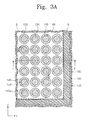
- a cell open mask pattern 160 may be formed on the sacrificial layer 140 of the peripheral region B to expose the cell region A, as illustrated in FIG. 3A .
- the cell open mask pattern 160 may cover the sacrificial layer 140 in the peripheral region B, while the sacrificial layer 140 and the assistance spacers 153 in the cell region A may be exposed by the cell open mask pattern 160 .
- the cell open mask pattern 160 may be formed of a material having an etch selectivity with respect to the sacrificial layer 140 , the assistance spacers 153 , and the mask layer 130 .
- the cell open mask pattern 160 may be formed of photoresist.
- the sacrificial layer 140 in the cell region A may be removed, such that, e.g., only, the assistance spacers 153 remain on the mask layer 130 in the cell region A.
- the sacrificial layer 140 in the cell region A may be removed by an isotropic etching process using an etchant having an etch selectivity with respect to the assistance spacers 153 and the mask layer 130 .
- a portion of the sacrificial layer 140 in the peripheral region B adjacent the cell region A may be removed simultaneously.
- a peripheral sacrificial pattern 140 a may be formed to expose a portion of the mask layer 130 of the peripheral region B in a boundary region between the peripheral region B and the cell region A.
- a small portion of the sacrificial layer 140 in the peripheral region B i.e., a portion at a boundary with and in contact with the cell region A, is removed, such that the remaining portion of the sacrificial layer 140 , i.e., the peripheral sacrificial pattern 140 a , may remain in the peripheral region B under the cell open mask pattern 160 . Therefore, the cell open mask pattern 160 may extend beyond the peripheral sacrificial pattern 140 a , i.e., the cell open mask pattern 160 may overlap the peripheral sacrificial pattern 140 a and a portion of the exposed mask layer 130 .
- first mask spacers 173 and a second mask spacer 175 may be formed on the mask layer 130 .
- a mask spacer layer 170 may be conformally formed on the assistance spacers 153 and the mask layer 130 . Then the mask spacer layer 170 may be anisotropically etched until the top surface of the mask layer 130 is exposed and the first mask spacers 173 and the second mask spacer 175 are formed. That is, portions of the mask spacer layer 170 on inner and outer sidewalls of the assistance spacers 153 may define the first and second mask spacers 173 and 175 , respectively.
- each of the first mask spacers 173 may be formed in the inner space 145 a defined by each of the assistance spacers 153 .
- each of the first mask spacers 173 may cover, e.g., continuously, an inner sidewall of each of the assistance spacers 153 .
- a first opening 145 b may be defined in each of the inner spaces 145 a by each of the first mask spacers 173 .
- cylindrical assistance spacers 153 may have the first mask spacers 173 on inner sidewalls thereof, such that the first mask spacers 173 may define the first openings 145 b to be concentric with the respective assistance spacers 153 .
- the first openings 145 b may be in centers of respective preliminary openings 145 and may be defined by the first mask spacers 173 to have smaller diameters than the preliminary openings 145 .
- the second mask spacer 175 may be formed in a space which is formed by removing the sacrificial layer 140 . That is, the second mask spacer 175 may cover outer sidewalls of the assistance spacers 153 , e.g., the second mask spacer 175 may be formed, e.g., continuously, between adjacent assistance spacers 153 . In some embodiments, the shortest distance between a pair of the assistance spacers 153 adjacent to each other in the first direction may be less than two times a deposition thickness of the mask spacer layer formed on the mask layer 130 and the assistance spacers 153 .
- the shortest distance between a pair of the assistance spacers 153 adjacent to each other in the second direction may be less than two times a deposition thickness of the mask spacer layer formed on the mask layer 130 and the assistance spacers 153 .
- a part of a space between the assistance spacers 153 adjacent to each other in the first direction may be filled with the second mask spacer 175 .
- a part of a space between the assistance spacers 153 adjacent to each other in the second direction may also be filled with the second mask spacer 175 .
- Second openings 145 c exposing the top surface of the mask layer 130 may be defined by the second mask spacer 175 .
- Each of the second openings 145 c may be defined between a pair of the assistance spacers 153 adjacent to each other in a third direction when viewed from a plan view ( FIG. 5A ).
- one second opening 145 c may be between two assistance spacers 153 adjacent to watch other along the third direction, e.g., a diagonal direction. Therefore, the first openings 145 b and the second openings 145 c may be arranged to alternate in the third direction. That is, the first openings 145 b and the second openings 145 c may be alternately and repeatedly arranged in the third direction.
- the third direction may be non-parallel and non-perpendicular to the first and second directions in a plan view.
- each of the second openings 145 c may be disposed among four assistance spacers 153 adjacent to each other when viewed from a plan view, e.g., one second opening 145 c may be disposed in a center of a square having its vertices defines by the first openings 145 b of respective four assistance spacers 153 .
- a mask trench 145 d exposing the mask layer 130 may be formed in the boundary region between the cell region A and the peripheral region B.
- the mask trench 145 d may be defined by the second mask spacer 175 and the peripheral sacrificial pattern 140 a.
- the mask layer 130 may be etched to form a cell mask pattern 135 a and a peripheral mask pattern 135 b .
- the cell mask pattern 135 a and the peripheral mask pattern 135 b may be formed by an anisotropic etching process using the assistance spacers 153 , the first mask spacers 173 , the second mask spacer 175 , and the peripheral sacrificial pattern 140 a as etch masks.
- the mask layer 130 may be divided into the cell mask pattern 135 a and the peripheral mask pattern 135 b by etching the mask layer 130 exposed by the mask trench 145 d.
- the cell mask pattern 135 a may have a plurality of mask holes 135 defined by the first openings 145 b and the second opening 145 c .
- portions of the mask layers exposed by the first openings 145 b and the second openings 145 c may be etched to form the mask holes 135 exposing the buffer oxide layer 125 .
- the second openings 145 c may have a polygon shape having vertices in a plan view.
- the amount of an etchant provided to a vertex region in the second opening 145 c may be less than the amount of the etchant provided to the other region in the second opening 145 c .
- an etch rate of a portion of the mask layer 130 exposed by the vertex region of the second opening 145 c may be less than an etch rate of a portion of the mask layer 130 exposed by the other region of the second opening 145 c .
- the mask holes 135 defined by the second openings 145 c may be formed to have circular shapes in a plan view.
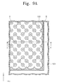
- the buffer oxide layer 125 , the supporting layer 123 , and the mold layer 110 may be successively etched using the cell mask pattern 135 a and the peripheral mask pattern 135 b as etch masks.
- a plurality of holes 115 a may be formed in the mold layer 110 in the cell region A.
- the holes 115 a may expose the substrate 100 .
- a distance between center points of a pair of the holes 115 a adjacent to each other in the first direction is represented as R 1
- a distance between center points of a pair of three holes 115 a adjacent to each other in the second direction is represented as R 2
- a distance between center points of a pair of the holes 115 a adjacent to each other in the third direction is represented as R 3 .
- a designator ‘ ⁇ ’ represents an angle between a straight line connecting the center points of the pair of the holes 115 a adjacent to each other in the first direction and a straight line connecting the center points of the pair of the holes 115 a adjacent to each other in the second direction. In some embodiments, the angle ⁇ may be 90 degrees.
- the R 3 may be represented as the following formula 1.
- R 3 (( R 1 2 +R 2 2 )/4) 1/2 [Formula 1]
- the R 1 may be equal to the R 2 .
- the R 3 may be R 1 /(2 1/2 ).
- the mold 110 in the boundary region between the cell region A and the peripheral region B may be etched to form a dummy trench 115 c .
- the dummy trench 115 c may expose the substrate 100 .
- the mold layer 110 in the peripheral region B may be separated from the mold layer 110 in the cell region A by the dummy trench 115 c.
- first electrodes 183 may be formed in the holes 115 a , respectively. Additionally, a dummy pattern 185 may be formed in the dummy trench 115 c .
- a first electrode layer may be conformally formed on the substrate 100 having the holes 115 a , and then the first electrode layer may be etched until the buffer oxide layer 125 is exposed. Thus, the first electrodes 183 and the dummy pattern 185 may be formed.
- the first electrode layer may be formed by using a PVD process, a CVD process, and/or an atomic layer deposition (ALD) process.
- each of the first electrodes 183 may completely fill each of the holes 115 a .
- the first electrode 183 may have a pillar shape.
- the dummy pattern 185 may also completely fill the dummy trench 115 c.
- the first electrodes 183 and the dummy pattern 185 may include at least one of a doped semiconductor, a conductive metal nitride (e.g., titanium nitride, tantalum nitride, and/or tungsten nitride, etc.), metal (e.g., ruthenium, iridium, titanium, and/or tantalum, etc.), and a conductive metal oxide (e.g., iridium oxide, etc.).
- a doped semiconductor e.g., a conductive metal nitride (e.g., titanium nitride, tantalum nitride, and/or tungsten nitride, etc.), metal (e.g., ruthenium, iridium, titanium, and/or tantalum, etc.), and a conductive metal oxide (e.g., iridium oxide, etc.).
- a conductive metal nitride e.g., titanium
- the buffer oxide layer 125 and the supporting layer 123 may be patterned to form a supporting pattern 123 a and a buffer oxide pattern 125 a .
- the supporting pattern 123 a and the buffer oxide pattern 125 a may expose portions of a top surface of the mold layer 110 .
- portions of the buffer oxide layer 125 and supporting layer 123 may be removed to expose, e.g., rectangular, regions of the mold layer 110 among a plurality of the first electrodes 183 .
- a plurality, e.g., six, of the first electrodes 183 may be arranged along a perimeter of the exposed region of the mold layer 110 , such that each first electrode 183 may be between the exposed region of the mold layer 110 and the remaining portion of the buffer oxide layer, i.e., the buffer oxide pattern 125 a .
- the supporting pattern 123 a may be in contact with at least a portion of each of the first electrodes 183 .
- the supporting pattern 123 a may function to support the first electrodes 183 . In other words, the supporting pattern 123 a may prevent the first electrodes 183 having a high aspect ratio from being electrically connected to each other by contact or lifting.
- the buffer oxide pattern 125 a and the mold layer 110 in the cell and peripheral regions A and B may be removed. Outer sidewalls of the first electrodes 183 may be exposed by removing the buffer oxide pattern 125 a and the mold layer 110 .
- the buffer oxide pattern 125 a and the mold layer 110 may be removed by an isotropic etching process using an etchant having an etch selectivity with respect to the supporting pattern 123 a .
- the mold layer 110 may be removed by a LAL lift-off process using a LAL solution including ammonium fluoride (NH 4 F), hydrofluoric acid (HF), and water.
- the mold layer 110 of the cell region A may be removed but the mold layer of the peripheral region B may not be removed.
- the mold layer 110 of the peripheral region B may remain, and the mold layer 110 of the cell region A may be removed.
- the dummy pattern 185 may function as a barrier preventing the etchant for removal of the mold layer 110 of the cell region A from etching the mold layer 110 of the peripheral region B.
- a capacitor dielectric layer 193 may be conformally formed on the substrate 100 .
- the capacitor dielectric layer 193 may be conformally formed along outer sidewalls, top surfaces, and inner surfaces of the first electrodes 183 , a surface of the supporting pattern 123 a , and the top surface of the substrate 100 .
- the capacitor dielectric layer 193 may include at least one of an oxide layer (e.g., a silicon oxide layer), a nitride layer (e.g., a silicon nitride layer), an oxynitride layer (e.g., a silicon oxynitride layer), and a high-k dielectric layer (e.g., a metal oxide layer such as a hafnium oxide layer and/or an aluminum oxide layer).
- an oxide layer e.g., a silicon oxide layer
- a nitride layer e.g., a silicon nitride layer
- an oxynitride layer e.g., a silicon oxynitride layer
- a high-k dielectric layer e.g., a metal oxide layer such as a hafnium oxide layer and/or an aluminum oxide layer.
- a second electrode layer 195 may be formed on the substrate 100 .
- the second electrode layer 195 may fill a space formed by removal of the mold layer 110 and inner spaces surrounded by the inner surfaces of the first electrodes 183 .
- the capacitor dielectric layer 193 may be disposed between the second electrode layer 195 and the first electrodes 183 and between the second electrode layer 195 and the supporting pattern 123 a .
- the second electrode layer 195 may include at least one of a doped semiconductor layer, a conductive metal nitride layer (e.g., a titanium nitride layer, tantalum nitride layer, and/or tungsten nitride layer, etc.), a metal layer (e.g., a ruthenium layer, an iridium layer, a titanium layer, and/or tantalum layer, etc.), and a conductive oxide layer (e.g., an iridium oxide layer, etc.).
- a conductive metal nitride layer e.g., a titanium nitride layer, tantalum nitride layer, and/or tungsten nitride layer, etc.
- a metal layer e.g., a ruthenium layer, an iridium layer, a titanium layer, and/or tantalum layer, etc.
- a conductive oxide layer e.g., an iridium oxide layer
- the first openings 145 b defined by the first mask spacers 173 and the second openings 145 c defined by the second mask spacer 175 may be formed on the mask layer 130 using the assistance spacers 153 for the formation of the holes 115 a .
- the first openings 145 b may be defined using the preliminary openings 145 defined by one photolithography process, the assistance spacers 153 , and the first mask spacers 173
- the second openings 145 c may be defined between the first openings 145 b in the third direction by the second mask spacer 175 . Therefore, formation of the second openings 145 c between the first openings 145 b in the third direction minimizes a distance between adjacent holes, thereby reducing a minimal distance defined by lithography equipment.
- FIGS. 11A to 15A are plan views illustrating stages in a method of forming a semiconductor memory device according to another embodiment of the inventive concept
- FIGS. 11B to 15B are cross-sectional views taken along lines I-I′ of FIGS. 11A to 15A , respectively.
- the method according to the present embodiment may include all processes described with reference to FIGS. 1A to 1C and 2 A to 2 C.
- a cell open mask pattern 163 may be formed on the sacrificial layer 140 of the peripheral region B to expose the cell region A.
- the cell open mask pattern 163 may cover the sacrificial layer 140 in the peripheral region B and a portion of the cell region A adjacent to the peripheral region B.
- the cell open mask pattern 163 may cover portions of the assistance spacers 153 arranged along one row and one column adjacent to the peripheral region B.
- the cell open mask pattern 163 may fill inner spaces 145 a defined by the assistance spacers 153 arranged along the one row and the one column adjacent to the peripheral region B.
- the cell open mask pattern 163 may be formed of a material having an etch selectivity with respect to the sacrificial layer 140 , the assistance spacers 153 , and the mask layer 130 .
- the cell open mask pattern 163 may be formed of photoresist.
- the sacrificial layer 140 of the cell region A may be removed.
- the sacrificial layer 140 may be removed by an isotropic etching process using an etchant having an etch selectivity with respect to the assistance spacer 153 and the mask layer 130 .
- the sacrificial layer 140 of the cell region A adjacent to the peripheral region B may remain.
- the sacrificial layer 140 of the peripheral region B and a portion of the sacrificial layer 140 of the cell region A adjacent to the peripheral region B may remain to form a peripheral sacrificial pattern 140 b .
- the remaining portion of the sacrificial layer 140 in the cell region A of the peripheral sacrificial pattern 140 b may cover portions of outer sidewalls of the assistance spacers 153 arranged along the one row and the one column adjacent to the peripheral region B.
- the first mask spacers 173 and the second mask spacer 175 may be formed on the mask layer 130 , as described with reference to FIGS. 5A to 5C .
- the first opening 145 b may be defined in the inner space 145 a by each of the first mask spacer 173
- the second openings 145 c exposing the top surface of the mask layer 130 may be defined by the second mask spacer 175 .
- the first openings 145 b and the second openings 145 c may have the same shape and be formed by the same method as described with reference to FIGS. 5A to 5C .
- the mask layer 130 may be etched to form a mask pattern 137 .
- the mask pattern 137 may be formed by an anisotropic etching process using the assistance spacers 153 , the first mask spacers 173 , the second mask spacer 175 , and the peripheral sacrificial pattern 140 b as etch masks.
- the mask pattern 137 may have a plurality of mask holes 135 defined by the first openings 145 b and the second openings 145 c .
- portions of the mask layer 130 exposed by the first openings 145 b and the second openings 145 c may be etched to form the mask holes 135 exposing the buffer oxide layer 125 .
- the buffer oxide layer 125 , the supporting layer 123 , and the mold layer 110 may be successively etched using the mask pattern 137 as an etch mask. Thus, a plurality of the holes 115 a may be formed in the mold layer 110 in the cell region A. The holes 115 a may expose the top surface of the substrate 100 .
- the mask pattern 137 of the cell region A may be connected to the mask pattern 137 of the peripheral region B, differently from the embodiment described with reference to FIGS. 1A to 10A , 1 B to 10 B, and 1 C to 7 C.
- the mask pattern 137 may cover the mold layer 110 in the peripheral region B and the boundary region between the cell region A and the peripheral region B.
- the mold layer 110 in the boundary region between the cell region A and the peripheral region B may not be etched, so that the mold layer 110 of the peripheral region B and the mold layer 110 of the cell region A may not be separated from each other, unlike the embodiment described with reference to FIGS. 1A to 10A , 1 B to 10 B, and 1 C to 7 C.
- the first electrodes 183 may be formed in the holes 115 a , respectively.
- the mold layer 110 of the peripheral region B and the mold layer 110 of the cell region A are separated from each other, so that a dummy pattern is not formed in the boundary region of the cell region A and the peripheral region B.
- the buffer oxide layer 125 and supporting layer 123 may be patterned to form the supporting pattern 123 a and the buffer oxide pattern 125 a .
- the mold layer 110 and the buffer oxide pattern 125 a may be removed.
- the mold layer 110 of the cell region A and the mold layer 110 of the peripheral region B may be removed simultaneously.
- a capacitor dielectric layer 193 may be conformally formed on the substrate 100 , and then a second electrode layer 195 may be formed on the substrate 100 .
- the method according to the present embodiment may achieve the same effect as the embodiment described with reference to FIGS. 1A to 10A , 1 B to 10 B, and 1 C to 7 C.
- the semiconductor memory devices according to embodiments described above may be encapsulated using various packaging techniques.
- the semiconductor memory devices according to the aforementioned embodiments may be encapsulated using any one of a package on package (POP) technique, a ball grid arrays (BGAs) technique, a chip scale packages (CSPs) technique, a plastic leaded chip carrier (PLCC) technique, a plastic dual in-line package (PDIP) technique, a die in waffle pack technique, a die in wafer form technique, a chip on board (COB) technique, a ceramic dual in-line package (CERDIP) technique, a plastic metric quad flat package (PMQFP) technique, a plastic quad flat package (PQFP) technique, a small outline package (SOIC) technique, a shrink small outline package (SSOP) technique, a thin small outline package (TSOP) technique, a thin quad flat package (TQFP) technique, a system in package (SIP) technique, a multi chip package (MCP) technique, a wafer
- the package in which the semiconductor memory device according to one of the above embodiments is mounted may further include at least one semiconductor device (e.g., a controller and/or a logic device) that controls the semiconductor memory device.
- at least one semiconductor device e.g., a controller and/or a logic device that controls the semiconductor memory device.
- FIG. 16 is a schematic block diagram illustrating an example of an electronic system including semiconductor memory devices according to embodiments of the inventive concept.
- an electronic system 1100 may include a controller 1110 , an input/output (I/O) unit 1120 , a memory device 1130 a , an interface unit 1140 , and a data bus 1150 .
- the controller 1110 , the I/O unit 1120 , the memory device 1130 a , and the interface unit 1140 may communicate with each other through the data bus 1150 .
- the data bus 1150 may correspond to a path through which electrical signals are transmitted.
- the controller 1110 may include, e.g., at least one of a microprocessor, a digital signal processor, a microcontroller, or another logic device.
- the other logic device may have a similar function to any one of the microprocessor, the digital signal processor, and the microcontroller.
- the I/O unit 1120 may include, e.g., a keypad, a keyboard, and/or a display unit.
- the memory device 1130 a may store data and/or commands.
- the memory device 1130 a may include at least one of the semiconductor memory devices according to the embodiments described above.
- the memory device 1130 a may further include other type of semiconductor memory devices which are different from the semiconductor devices described above.
- the memory device 1130 may further include a non-volatile memory device (e.g. a flash memory device, a magnetic memory device, a phase change memory device, etc) and/or a static random access memory (SRAM) device.
- the interface unit 1140 may transmit electrical data to a communication network or may receive electrical data from a communication network.
- the interface unit 1140 may operate by wireless or cable.
- the interface unit 1140 may include an antenna for wireless communication or a transceiver for cable communication.
- the electronic system 1100 may further include a fast DRAM device and/or a fast SRAM device which acts as a cache memory for improving an operation of the controller 1110 .
- the electronic system 1100 may be applied to, e.g., a personal digital assistant (PDA), a portable computer, a web tablet, a wireless phone, a mobile phone, a digital music player, a memory card, or other electronic products.
- PDA personal digital assistant
- the other electronic products may receive or transmit information data by wireless.
- FIG. 17 is a schematic block diagram illustrating an example of a memory card including semiconductor memory devices according to embodiments of the inventive concept.
- a memory card 1200 may include a memory device 1210 .
- the memory device 1210 may include at least one of the semiconductor memory devices according to the embodiments mentioned above. In other embodiments, the memory device 1210 may further include other types of semiconductor memory devices which are different from the semiconductor devices according to the embodiments described above.
- the memory device 1210 may further include a non-volatile memory device (e.g. a flash memory device, a magnetic memory device, a phase change memory device, etc) and/or a static random access memory (SRAM) device.
- the memory card 1200 may include a memory controller 1220 that controls data communication between a host and the memory device 1210 .
- the memory controller 1220 may include a central processing unit (CPU) 1222 that controls overall operations of the memory card 1200 .
- the memory controller 1220 may include a SRAM device 1221 used as an operation memory of the CPU 1222 .
- the memory controller 1220 may further include a host interface unit 1223 and a memory interface unit 1225 .
- the host interface unit 1223 may be configured to include a data communication protocol between the memory card 1200 and the host.
- the memory interface unit 1225 may connect the memory controller 1220 to the memory device 1210 .
- the memory controller 1220 may further include an error check and correction (ECC) block 1224 .
- ECC error check and correction
- the memory card 1200 may further include a read only memory (ROM) device that stores code data to interface with the host.
- ROM read only memory
- the memory card 1200 may be used as a portable data storage card.
- the memory card 1200 may be realized as solid state disks (SSD) which are used as hard disks of computer systems.
- the first openings may be defined using the assistance spacers and the first mask spacers in the preliminary openings formed by the lithography process, and the second openings may be defined between the first openings by the assistance spacers and the second mask spacer.
Landscapes
- Engineering & Computer Science (AREA)
- Power Engineering (AREA)
- Computer Hardware Design (AREA)
- Microelectronics & Electronic Packaging (AREA)
- Physics & Mathematics (AREA)
- Condensed Matter Physics & Semiconductors (AREA)
- General Physics & Mathematics (AREA)
- Manufacturing & Machinery (AREA)
- Chemical & Material Sciences (AREA)
- Inorganic Chemistry (AREA)
- General Engineering & Computer Science (AREA)
- Semiconductor Memories (AREA)
Applications Claiming Priority (2)
| Application Number | Priority Date | Filing Date | Title |
|---|---|---|---|
| KR1020110106019A KR101751476B1 (ko) | 2011-10-17 | 2011-10-17 | 반도체 기억 소자의 형성 방법 |
| KR10-2011-0106019 | 2011-10-17 |
Publications (2)
| Publication Number | Publication Date |
|---|---|
| US20130095663A1 US20130095663A1 (en) | 2013-04-18 |
| US8772167B2 true US8772167B2 (en) | 2014-07-08 |
Family
ID=48086284
Family Applications (1)
| Application Number | Title | Priority Date | Filing Date |
|---|---|---|---|
| US13/587,996 Active US8772167B2 (en) | 2011-10-17 | 2012-08-17 | Method of forming a semiconductor memory device |
Country Status (2)
| Country | Link |
|---|---|
| US (1) | US8772167B2 (ko) |
| KR (1) | KR101751476B1 (ko) |
Cited By (1)
| Publication number | Priority date | Publication date | Assignee | Title |
|---|---|---|---|---|
| US10096603B2 (en) | 2015-08-19 | 2018-10-09 | Samsung Electronics Co., Ltd. | Method of fabricating semiconductor device |
Families Citing this family (8)
| Publication number | Priority date | Publication date | Assignee | Title |
|---|---|---|---|---|
| KR102037874B1 (ko) | 2013-02-07 | 2019-10-29 | 삼성전자주식회사 | 반도체 소자의 홀 패턴들을 형성하는 방법 |
| US9123772B2 (en) * | 2013-10-02 | 2015-09-01 | GlobalFoundries, Inc. | FinFET fabrication method |
| US9379010B2 (en) * | 2014-01-24 | 2016-06-28 | Intel Corporation | Methods for forming interconnect layers having tight pitch interconnect structures |
| KR102224847B1 (ko) * | 2014-10-10 | 2021-03-08 | 삼성전자주식회사 | 반도체 소자의 제조방법 |
| KR20160085043A (ko) | 2015-01-07 | 2016-07-15 | 에스케이하이닉스 주식회사 | 패턴 형성 방법 |
| US9558956B2 (en) * | 2015-07-01 | 2017-01-31 | Samsung Electronics Co., Ltd. | Method for fabricating semiconductor device |
| KR102411071B1 (ko) * | 2017-05-29 | 2022-06-21 | 삼성전자주식회사 | 반도체 장치 |
| CN110707044B (zh) * | 2018-09-27 | 2022-03-29 | 联华电子股份有限公司 | 形成半导体装置布局的方法 |
Citations (3)
| Publication number | Priority date | Publication date | Assignee | Title |
|---|---|---|---|---|
| KR20010073304A (ko) | 2000-01-13 | 2001-08-01 | 윤종용 | 반도체 소자의 미세 패턴 형성 방법 |
| US20100120258A1 (en) * | 2008-11-13 | 2010-05-13 | Won-Kyu Kim | Method for forming micro-pattern in semiconductor device |
| KR20100102422A (ko) | 2009-03-11 | 2010-09-24 | 주식회사 하이닉스반도체 | 스페이서 패터닝 공정을 이용한 콘택홀 형성 방법 |
Family Cites Families (1)
| Publication number | Priority date | Publication date | Assignee | Title |
|---|---|---|---|---|
| US7291560B2 (en) * | 2005-08-01 | 2007-11-06 | Infineon Technologies Ag | Method of production pitch fractionizations in semiconductor technology |
-
2011
- 2011-10-17 KR KR1020110106019A patent/KR101751476B1/ko active IP Right Grant
-
2012
- 2012-08-17 US US13/587,996 patent/US8772167B2/en active Active
Patent Citations (4)
| Publication number | Priority date | Publication date | Assignee | Title |
|---|---|---|---|---|
| KR20010073304A (ko) | 2000-01-13 | 2001-08-01 | 윤종용 | 반도체 소자의 미세 패턴 형성 방법 |
| US20100120258A1 (en) * | 2008-11-13 | 2010-05-13 | Won-Kyu Kim | Method for forming micro-pattern in semiconductor device |
| KR20100053852A (ko) | 2008-11-13 | 2010-05-24 | 주식회사 하이닉스반도체 | 반도체 소자의 미세 패턴 형성방법 |
| KR20100102422A (ko) | 2009-03-11 | 2010-09-24 | 주식회사 하이닉스반도체 | 스페이서 패터닝 공정을 이용한 콘택홀 형성 방법 |
Cited By (1)
| Publication number | Priority date | Publication date | Assignee | Title |
|---|---|---|---|---|
| US10096603B2 (en) | 2015-08-19 | 2018-10-09 | Samsung Electronics Co., Ltd. | Method of fabricating semiconductor device |
Also Published As
| Publication number | Publication date |
|---|---|
| KR101751476B1 (ko) | 2017-06-28 |
| KR20130041630A (ko) | 2013-04-25 |
| US20130095663A1 (en) | 2013-04-18 |
Similar Documents
| Publication | Publication Date | Title |
|---|---|---|
| US8772167B2 (en) | Method of forming a semiconductor memory device | |
| US9153639B2 (en) | Memory devices with vertical storage node bracing and methods of fabricating the same | |
| US9853032B2 (en) | Semiconductor devices and methods for fabricating the same | |
| US9178026B2 (en) | Semiconductor devices and methods fabricating same | |
| US9287349B2 (en) | Semiconductor memory devices and methods of forming the same | |
| US9070640B2 (en) | Method of forming fine patterns of semiconductor device | |
| US8785319B2 (en) | Methods for forming fine patterns of a semiconductor device | |
| US20140110816A1 (en) | Semiconductor devices | |
| CN105336584B (zh) | 细微图案化方法以及利用该方法制造半导体器件的方法 | |
| US8816418B2 (en) | Semiconductor memory devices and methods of fabricating the same | |
| US20150340459A1 (en) | Method of forming patterns of semiconductor device | |
| US9147685B2 (en) | Semiconductor memory devices including support patterns | |
| US9087728B2 (en) | Semiconductor device | |
| US9053971B2 (en) | Semiconductor devices having hybrid capacitors and methods for fabricating the same | |
| US9911828B2 (en) | Methods of fabricating a semiconductor device | |
| KR20150019138A (ko) | 일체형의 지지대를 구비한 반도체 소자 | |
| US20150333059A1 (en) | Semiconductor devices including isolation gate lines between active patterns and methods of manufacturing the same | |
| KR102366804B1 (ko) | 반도체 소자의 제조 방법 | |
| US9293336B2 (en) | Semiconductor device and method of fabricating the same | |
| US9589964B1 (en) | Methods of fabricating semiconductor devices | |
| US20140061743A1 (en) | Semiconductor devices and method of fabricating the same | |
| US8953356B2 (en) | Semiconductor devices | |
| KR20140087357A (ko) | 반도체 장치의 캐패시터 및 그 제조방법 | |
| KR20170109874A (ko) | 반도체 장치 및 그의 제조 방법 | |
| CN116133384A (zh) | 半导体结构及其形成方法 |
Legal Events
| Date | Code | Title | Description |
|---|---|---|---|
| AS | Assignment |
Owner name: SAMSUNG ELECTRONICS CO., LTD., KOREA, REPUBLIC OF Free format text: ASSIGNMENT OF ASSIGNORS INTEREST;ASSIGNORS:SEO, JUNGWOO;YOON, KYOUNG RYUL;YOON, KUKHAN;REEL/FRAME:028802/0924 Effective date: 20120704 |
|
| STCF | Information on status: patent grant |
Free format text: PATENTED CASE |
|
| MAFP | Maintenance fee payment |
Free format text: PAYMENT OF MAINTENANCE FEE, 4TH YEAR, LARGE ENTITY (ORIGINAL EVENT CODE: M1551) Year of fee payment: 4 |
|
| MAFP | Maintenance fee payment |
Free format text: PAYMENT OF MAINTENANCE FEE, 8TH YEAR, LARGE ENTITY (ORIGINAL EVENT CODE: M1552); ENTITY STATUS OF PATENT OWNER: LARGE ENTITY Year of fee payment: 8 |