US8750024B2 - Memcapacitor - Google Patents
Memcapacitor Download PDFInfo
- Publication number
- US8750024B2 US8750024B2 US13/256,245 US200913256245A US8750024B2 US 8750024 B2 US8750024 B2 US 8750024B2 US 200913256245 A US200913256245 A US 200913256245A US 8750024 B2 US8750024 B2 US 8750024B2
- Authority
- US
- United States
- Prior art keywords
- memcapacitive
- electrode
- matrix
- memcapacitor
- capacitance
- Prior art date
- Legal status (The legal status is an assumption and is not a legal conclusion. Google has not performed a legal analysis and makes no representation as to the accuracy of the status listed.)
- Active, expires
Links
- 239000002019 doping agent Substances 0.000 claims abstract description 81
- 239000011159 matrix material Substances 0.000 claims abstract description 81
- 238000000034 method Methods 0.000 claims abstract description 17
- 239000004020 conductor Substances 0.000 claims description 21
- 230000000903 blocking effect Effects 0.000 claims description 13
- 239000003989 dielectric material Substances 0.000 claims description 5
- 238000010438 heat treatment Methods 0.000 claims description 3
- 230000001419 dependent effect Effects 0.000 claims description 2
- 150000002500 ions Chemical class 0.000 abstract description 85
- 239000000370 acceptor Substances 0.000 description 34
- 239000002070 nanowire Substances 0.000 description 30
- 239000003990 capacitor Substances 0.000 description 25
- 239000000463 material Substances 0.000 description 15
- 230000005684 electric field Effects 0.000 description 14
- 238000010586 diagram Methods 0.000 description 11
- WHXSMMKQMYFTQS-UHFFFAOYSA-N Lithium Chemical compound [Li] WHXSMMKQMYFTQS-UHFFFAOYSA-N 0.000 description 10
- XUIMIQQOPSSXEZ-UHFFFAOYSA-N Silicon Chemical compound [Si] XUIMIQQOPSSXEZ-UHFFFAOYSA-N 0.000 description 10
- 229910052744 lithium Inorganic materials 0.000 description 10
- 230000037230 mobility Effects 0.000 description 10
- 229910052710 silicon Inorganic materials 0.000 description 10
- 239000010703 silicon Substances 0.000 description 10
- 239000004065 semiconductor Substances 0.000 description 9
- ZOXJGFHDIHLPTG-UHFFFAOYSA-N Boron Chemical compound [B] ZOXJGFHDIHLPTG-UHFFFAOYSA-N 0.000 description 8
- 229910052796 boron Inorganic materials 0.000 description 8
- 238000009792 diffusion process Methods 0.000 description 8
- 230000006399 behavior Effects 0.000 description 6
- 230000006870 function Effects 0.000 description 6
- QVGXLLKOCUKJST-UHFFFAOYSA-N atomic oxygen Chemical compound [O] QVGXLLKOCUKJST-UHFFFAOYSA-N 0.000 description 4
- 238000013500 data storage Methods 0.000 description 4
- 238000009826 distribution Methods 0.000 description 4
- 239000001301 oxygen Substances 0.000 description 4
- 229910052760 oxygen Inorganic materials 0.000 description 4
- 230000008901 benefit Effects 0.000 description 3
- 230000008859 change Effects 0.000 description 3
- 230000007423 decrease Effects 0.000 description 3
- 229910052732 germanium Inorganic materials 0.000 description 3
- GNPVGFCGXDBREM-UHFFFAOYSA-N germanium atom Chemical compound [Ge] GNPVGFCGXDBREM-UHFFFAOYSA-N 0.000 description 3
- 230000001537 neural effect Effects 0.000 description 3
- 230000008569 process Effects 0.000 description 3
- 239000000126 substance Substances 0.000 description 3
- IJGRMHOSHXDMSA-UHFFFAOYSA-N Atomic nitrogen Chemical compound N#N IJGRMHOSHXDMSA-UHFFFAOYSA-N 0.000 description 2
- GWEVSGVZZGPLCZ-UHFFFAOYSA-N Titan oxide Chemical compound O=[Ti]=O GWEVSGVZZGPLCZ-UHFFFAOYSA-N 0.000 description 2
- MCMNRKCIXSYSNV-UHFFFAOYSA-N Zirconium dioxide Chemical compound O=[Zr]=O MCMNRKCIXSYSNV-UHFFFAOYSA-N 0.000 description 2
- 229910052782 aluminium Inorganic materials 0.000 description 2
- XAGFODPZIPBFFR-UHFFFAOYSA-N aluminium Chemical compound [Al] XAGFODPZIPBFFR-UHFFFAOYSA-N 0.000 description 2
- 238000013461 design Methods 0.000 description 2
- 239000010416 ion conductor Substances 0.000 description 2
- 230000007774 longterm Effects 0.000 description 2
- 230000014759 maintenance of location Effects 0.000 description 2
- 230000000717 retained effect Effects 0.000 description 2
- 239000007787 solid Substances 0.000 description 2
- OKTJSMMVPCPJKN-UHFFFAOYSA-N Carbon Chemical compound [C] OKTJSMMVPCPJKN-UHFFFAOYSA-N 0.000 description 1
- ZAMOUSCENKQFHK-UHFFFAOYSA-N Chlorine atom Chemical compound [Cl] ZAMOUSCENKQFHK-UHFFFAOYSA-N 0.000 description 1
- VYZAMTAEIAYCRO-UHFFFAOYSA-N Chromium Chemical compound [Cr] VYZAMTAEIAYCRO-UHFFFAOYSA-N 0.000 description 1
- 229910021591 Copper(I) chloride Inorganic materials 0.000 description 1
- GYHNNYVSQQEPJS-UHFFFAOYSA-N Gallium Chemical compound [Ga] GYHNNYVSQQEPJS-UHFFFAOYSA-N 0.000 description 1
- HBBGRARXTFLTSG-UHFFFAOYSA-N Lithium ion Chemical compound [Li+] HBBGRARXTFLTSG-UHFFFAOYSA-N 0.000 description 1
- BQCADISMDOOEFD-UHFFFAOYSA-N Silver Chemical compound [Ag] BQCADISMDOOEFD-UHFFFAOYSA-N 0.000 description 1
- 229910002370 SrTiO3 Inorganic materials 0.000 description 1
- -1 Sulfide Ions Chemical class 0.000 description 1
- 229910003081 TiO2−x Inorganic materials 0.000 description 1
- 229910003360 ZrO2−x Inorganic materials 0.000 description 1
- 230000003044 adaptive effect Effects 0.000 description 1
- 238000003491 array Methods 0.000 description 1
- 238000013528 artificial neural network Methods 0.000 description 1
- 230000005540 biological transmission Effects 0.000 description 1
- 210000004556 brain Anatomy 0.000 description 1
- 230000003139 buffering effect Effects 0.000 description 1
- 229910052799 carbon Inorganic materials 0.000 description 1
- 229910052800 carbon group element Inorganic materials 0.000 description 1
- 238000005229 chemical vapour deposition Methods 0.000 description 1
- 239000000460 chlorine Substances 0.000 description 1
- 229910052801 chlorine Inorganic materials 0.000 description 1
- 229910052804 chromium Inorganic materials 0.000 description 1
- 239000011651 chromium Substances 0.000 description 1
- 150000001875 compounds Chemical class 0.000 description 1
- 238000010276 construction Methods 0.000 description 1
- OXBLHERUFWYNTN-UHFFFAOYSA-M copper(I) chloride Chemical compound [Cu]Cl OXBLHERUFWYNTN-UHFFFAOYSA-M 0.000 description 1
- 238000000151 deposition Methods 0.000 description 1
- 230000008021 deposition Effects 0.000 description 1
- 238000006073 displacement reaction Methods 0.000 description 1
- 230000000694 effects Effects 0.000 description 1
- 239000007772 electrode material Substances 0.000 description 1
- 230000008030 elimination Effects 0.000 description 1
- 238000003379 elimination reaction Methods 0.000 description 1
- 239000003574 free electron Substances 0.000 description 1
- 229910052733 gallium Inorganic materials 0.000 description 1
- CJNBYAVZURUTKZ-UHFFFAOYSA-N hafnium(IV) oxide Inorganic materials O=[Hf]=O CJNBYAVZURUTKZ-UHFFFAOYSA-N 0.000 description 1
- 238000002347 injection Methods 0.000 description 1
- 239000007924 injection Substances 0.000 description 1
- 239000011810 insulating material Substances 0.000 description 1
- 239000012212 insulator Substances 0.000 description 1
- 230000003993 interaction Effects 0.000 description 1
- 238000000025 interference lithography Methods 0.000 description 1
- 229910001416 lithium ion Inorganic materials 0.000 description 1
- 238000005259 measurement Methods 0.000 description 1
- 230000005055 memory storage Effects 0.000 description 1
- 229910052751 metal Inorganic materials 0.000 description 1
- 239000002184 metal Substances 0.000 description 1
- 239000002905 metal composite material Substances 0.000 description 1
- 229910001092 metal group alloy Inorganic materials 0.000 description 1
- 239000007769 metal material Substances 0.000 description 1
- 150000002739 metals Chemical class 0.000 description 1
- 238000012986 modification Methods 0.000 description 1
- 230000004048 modification Effects 0.000 description 1
- 229910052757 nitrogen Inorganic materials 0.000 description 1
- 230000000737 periodic effect Effects 0.000 description 1
- 238000000206 photolithography Methods 0.000 description 1
- 238000012545 processing Methods 0.000 description 1
- 230000009257 reactivity Effects 0.000 description 1
- 238000000926 separation method Methods 0.000 description 1
- 229910052709 silver Inorganic materials 0.000 description 1
- 239000004332 silver Substances 0.000 description 1
- 239000011800 void material Substances 0.000 description 1
Images


Classifications
-
- G—PHYSICS
- G11—INFORMATION STORAGE
- G11C—STATIC STORES
- G11C11/00—Digital stores characterised by the use of particular electric or magnetic storage elements; Storage elements therefor
- G11C11/21—Digital stores characterised by the use of particular electric or magnetic storage elements; Storage elements therefor using electric elements
- G11C11/24—Digital stores characterised by the use of particular electric or magnetic storage elements; Storage elements therefor using electric elements using capacitors
-
- G—PHYSICS
- G11—INFORMATION STORAGE
- G11C—STATIC STORES
- G11C13/00—Digital stores characterised by the use of storage elements not covered by groups G11C11/00, G11C23/00, or G11C25/00
- G11C13/0002—Digital stores characterised by the use of storage elements not covered by groups G11C11/00, G11C23/00, or G11C25/00 using resistive RAM [RRAM] elements
-
- H—ELECTRICITY
- H01—ELECTRIC ELEMENTS
- H01G—CAPACITORS; CAPACITORS, RECTIFIERS, DETECTORS, SWITCHING DEVICES OR LIGHT-SENSITIVE DEVICES, OF THE ELECTROLYTIC TYPE
- H01G4/00—Fixed capacitors; Processes of their manufacture
- H01G4/002—Details
- H01G4/018—Dielectrics
- H01G4/06—Solid dielectrics
- H01G4/08—Inorganic dielectrics
- H01G4/12—Ceramic dielectrics
- H01G4/1272—Semiconductive ceramic capacitors
-
- H—ELECTRICITY
- H01—ELECTRIC ELEMENTS
- H01G—CAPACITORS; CAPACITORS, RECTIFIERS, DETECTORS, SWITCHING DEVICES OR LIGHT-SENSITIVE DEVICES, OF THE ELECTROLYTIC TYPE
- H01G4/00—Fixed capacitors; Processes of their manufacture
- H01G4/002—Details
- H01G4/255—Means for correcting the capacitance value
-
- H—ELECTRICITY
- H01—ELECTRIC ELEMENTS
- H01G—CAPACITORS; CAPACITORS, RECTIFIERS, DETECTORS, SWITCHING DEVICES OR LIGHT-SENSITIVE DEVICES, OF THE ELECTROLYTIC TYPE
- H01G4/00—Fixed capacitors; Processes of their manufacture
- H01G4/33—Thin- or thick-film capacitors
-
- H—ELECTRICITY
- H01—ELECTRIC ELEMENTS
- H01L—SEMICONDUCTOR DEVICES NOT COVERED BY CLASS H10
- H01L27/00—Devices consisting of a plurality of semiconductor or other solid-state components formed in or on a common substrate
- H01L27/02—Devices consisting of a plurality of semiconductor or other solid-state components formed in or on a common substrate including semiconductor components specially adapted for rectifying, oscillating, amplifying or switching and having at least one potential-jump barrier or surface barrier; including integrated passive circuit elements with at least one potential-jump barrier or surface barrier
- H01L27/04—Devices consisting of a plurality of semiconductor or other solid-state components formed in or on a common substrate including semiconductor components specially adapted for rectifying, oscillating, amplifying or switching and having at least one potential-jump barrier or surface barrier; including integrated passive circuit elements with at least one potential-jump barrier or surface barrier the substrate being a semiconductor body
- H01L27/10—Devices consisting of a plurality of semiconductor or other solid-state components formed in or on a common substrate including semiconductor components specially adapted for rectifying, oscillating, amplifying or switching and having at least one potential-jump barrier or surface barrier; including integrated passive circuit elements with at least one potential-jump barrier or surface barrier the substrate being a semiconductor body including a plurality of individual components in a repetitive configuration
- H01L27/101—Devices consisting of a plurality of semiconductor or other solid-state components formed in or on a common substrate including semiconductor components specially adapted for rectifying, oscillating, amplifying or switching and having at least one potential-jump barrier or surface barrier; including integrated passive circuit elements with at least one potential-jump barrier or surface barrier the substrate being a semiconductor body including a plurality of individual components in a repetitive configuration including resistors or capacitors only
-
- H—ELECTRICITY
- H01—ELECTRIC ELEMENTS
- H01L—SEMICONDUCTOR DEVICES NOT COVERED BY CLASS H10
- H01L28/00—Passive two-terminal components without a potential-jump or surface barrier for integrated circuits; Details thereof; Multistep manufacturing processes therefor
- H01L28/40—Capacitors
Definitions
- dopants within an insulating or semiconducting matrix can dramatically alter the electrical characteristics and behavior of a device which incorporates the matrix.
- the electrical behavior of the device can be dynamically altered by the spatial redistribution of the dopants.
- the motion of dopants can be induced by the application of a programming electrical field or programming voltage pulse across the matrix. After removal of the electrical field, the location and characteristics of the dopants remain stable until the application of another programming electrical field or voltage pulse.
- the various dopant configurations are a form of “memory” retained within the device which corresponds to past electrical conditions. According to one illustrative embodiment, changes in dopant positions can alter the capacitance of the device.
- memcapacitors Devices which exhibit a “memory” of past electrical conditions based on changes in capacitance are often called “memcapacitors” or “memcapacitive devices.” Memcapacitive behavior is most strongly evident in nanometer scale devices, where a standard driving voltage produces large electric fields. These memcapacitors could potentially be used for high density data storage, circuit calibration, or to provide self programming, fuzzy logic, or neural learning capabilities.
- FIG. 1A is a diagram of an illustrative memcapacitor in a low capacitance state, according to one embodiment of principles described herein.
- FIG. 1B is a diagram of an illustrative circuit schematic for a memcapacitor in a low capacitance state, according to one embodiment of principles described herein.
- FIG. 1C is a diagram showing illustrative electrical potentials and dopant distributions in various regions of a memcapacitor in a low capacitance state, according to one embodiment of principles described herein.
- FIG. 1D is a diagram of an illustrative memcapacitor in a high capacitance state, according to one embodiment of principles described herein.
- FIG. 1E is a diagram of an illustrative circuit schematic for a memcapacitor in a high capacitance state, according to one embodiment of principles described herein.
- FIG. 1F is a diagram showing illustrative electrical potentials and dopant distributions in various regions of a memcapacitor in a high capacitance state, according to one embodiment of principles described herein.
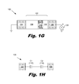
- FIG. 1G is a diagram showing the illustrative memcapacitor returning back to a low capacitance state, according to one embodiment of principles described herein.
- FIG. 1H is a diagram of an illustrative circuit schematic for a memcapacitor which has been returned to its low capacitance state, according to one embodiment of principles described herein.
- FIG. 2 is a graph which shows the diffusivity of various dopants in a silicon matrix as a function of temperature, according to one embodiment of principles described herein.
- FIGS. 3A and 3B are diagrams of alternative embodiments of memcapacitive devices, according to one embodiment of principles described herein.
- FIG. 4 is an isometric view of an illustrative nanowire crossbar architecture incorporating memcapacitive devices, according to one embodiment of principles described herein.
- FIG. 5 is a flow chart depicting an illustrative method for using a memcapacitor for data storage, according to one embodiment of principles described herein.
- electrical components which retain a memory of past conditions.
- these electrical components could be used to store data, calibrate circuits, or provide self programming, fuzzy logic, or neural learning capabilities.
- An example of such an electrical component may be a solid state memory device with high storage density, no power requirement for long term data retention, and fast access times.
- systems which could benefit from a retained memory of past conditions may include: switching devices; self programming circuit elements; memory devices capable of multi-state storage; solid state elements which can be used to tune circuits; analog neuronal computing devices which share fundamental functionalities with the human brain; and electronic devices for applying fuzzy logic processes.
- dopants within an insulating or semiconducting matrix can dramatically alter the electrical characteristics of the device.
- dopants can be introduced into a matrix or moved within a matrix to dynamically alter the electrical capacitance of the device.
- the motion of dopants can be induced by the application of a programming electrical field or voltage pulse across a suitable matrix. After removal of the electrical field or voltage pulse, the location and characteristics of the dopants remain stable until the application of another programming electrical field or voltage pulse.
- a memcapacitive device may be a programmable capacitor or “memcapacitor.”
- the term “memcapacitor” is derived from the combination of the two terms “memory” and “capacitor.”
- a capacitor is a fundamental circuit element comprised of two electric conductors with a dielectric material in between. Capacitance is a measurement of the ability of the capacitor to hold electrical charge. Capacitance is related to the overlapping area of the two conductors, the distance between the conductors and the permittivity of the dielectric medium which separates the conductors. For a parallel plate capacitor, the capacitance is given by Eq. 1, below.
- A the area of overlap between the two plates in square meters
- ⁇ r the dielectric constant of the insulator between plates
- a capacitor may be able to alter its capacitance based on experienced electrical conditions. The magnitude of the capacitance exhibited by the device may then be indicative of past electrical conditions. Electrical conditions which may change the locations of dopants within the memcapacitor include, but are not limited to, electrical fields, resistance induced heating, electrical current, and their combinations.
- the displacement state of the dopants allows the memcapacitor to “remember” how much voltage was previously applied and for how long.
- the motion of these dopants may alter the capacitance of the memcapacitor in a variety of ways.
- the dopant motion may increase or decrease the effective distance between charged surfaces.
- the dopant motion may increase or decrease the surface area over which the charge acts or the permittivity of the insulating material separating the charged plates.
- the dopants remain in this displaced state over long periods of time, thereby retaining a memory of the past electrical fields applied to the device. Until another electrical field is applied to the memcapacitor which has sufficient intensity or duration to induce dopant motion, the capacitance characteristics of the memcapacitor are substantially stable.
- memcapacitor or “memcapacitive” is used to describe a combination of an insulating/semiconductor matrix and a dopant which exhibits dopant motion in the presence of a programming electrical field and the desired long term dopant stability within the matrix when the programming field is removed.
- the memcapacitive effect is most strongly evident in nanometer scale devices and allows the device to “remember” past electrical conditions.
- FIG. 1A shows an illustrative two-terminal memcapacitor ( 100 ).
- the two-terminal memcapacitor ( 100 ) is comprised of a first electrode ( 104 ) and a second electrode ( 106 ), both of which are in electrical and physical contact with one of two blocking layers ( 114 , 115 ).
- a memcapacitive matrix ( 102 ) is disposed between the blocking layers ( 114 , 115 ).
- the memcapacitive matrix ( 102 ) is made up of a lightly doped semiconductor region ( 108 , 112 ) and an acceptor layer ( 110 ) which contains a number of mobile ions ( 111 ).
- the electrodes ( 104 , 106 ) may be constructed from a variety of conducting materials, including but not limited to: metals, metal alloys, metal composite materials, nano-structured metal materials, or other suitable conducting materials.
- the electrodes ( 104 , 106 ) may be comprised of one or more layers. According to one illustrative embodiment, the electrodes ( 104 , 106 ) have two layers: a first conducting layer which generally has low reactivity with the surrounding materials; and a metallic adhesion layer.
- the metallic adhesion layer can be, for example, aluminum or chromium.
- the term “memcapacitive matrix” describes a weakly ionic conductive material which is capable of transporting and hosting ions that act as dopants to control the flow of electrons through the memcapacitor.
- the definition of a weakly ionic conductive material is based on the application for which the memcapacitive device is designed.
- the mobility and the diffusion constant for a dopant species in a lattice are directly proportional to one another, via the “Einstein relation”. Thus, if the mobility of ionized species in a lattice is very high, so is the diffusion constant.
- the memcapacitive device In general, it is desired for the memcapacitive device to stay in a particular state, either low or high capacitance, for an amount of time that may range from a fraction of a second to years, depending on the application.
- the diffusion constant for such a device is, in one embodiment, low enough to ensure the desired level of stability. This desired level of stability avoids inadvertently turning the device from low capacitance to a high capacitance state or vice versa via ionized species diffusion, but allows the intentionally setting the state of the switch with a voltage pulse.
- a “weakly ionic conductor” is one in which the ion mobility, and thus the diffusion constant, is small enough to ensure the stability of the state of the device for as long as necessary under the desired conditions (e.g., the device does not change state because of diffusion of the dopants).
- “strongly ionic conductors” would have large ionized species mobilities and thus would not be stable against diffusion.
- Suitable memcapacitive matrix materials are given in Table 1, below.
- the table lists compatible primary materials, secondary materials, and dopant species for each memcapacitive combinations.
- the primary material is typically a highly insulating stoichiometric compound.
- the secondary material is the doped version of the primary material.
- Table 1 is lists only illustrative examples of possible matrix and dopant combinations and is not exhaustive. A variety of other matrix/dopant combinations could be used. For example, in addition to lithium, a number of other mobile dopant species could be used in a silicon matrix. Further, other matrix materials, such as germanium, could be used with appropriate dopant species to form a memcapacitive device.
- the basic mode of operation is to apply a negative voltage pulse to the electrode ( 106 ) closest to the acceptor layer ( 110 ) large enough to heat and redistribute the mobile ions ( 111 ) into one of the lightly doped semiconducting regions ( 108 , 112 ).
- the mobile ions ( 111 ) are specifically chosen from those that act as electrical dopants for the memcapacitive matrix ( 102 ), and thereby varying the capacitance of the device.
- the memcapacitive matrix ( 102 ) and the dopant species are chosen such that the drift of the dopants ( 111 ) within the memcapacitive matrix ( 102 ) is possible but not too facile, to ensure that the device ( 100 ) will remain in whatever state it is set for a reasonably long time, perhaps many years at room temperature. This ensures that the memcapacitive device ( 100 ) is nonvolatile, that is, that it holds its state after the programming voltage has been removed. The memcapacitive device ( 100 ) can then act as a storage element which can be read multiple times and remains stable over the desired duration.
- the semiconducting regions ( 108 , 112 ) within the memcapacitive matrix ( 102 ) may be made up of a variety of semi-conductive material and is in many cases nanocrystalline or amorphous. There are many materials which could be used to makeup the semiconducting regions ( 108 , 112 ) including but not limited to silicon and germanium.
- the acceptor layer ( 110 ) within the memcapacitive matrix ( 102 ) may be made of a semiconductor material doped with acceptor atoms.
- the purpose of the acceptor layer ( 110 ) is to form a region within the memcapacitive matrix ( 102 ) in which the mobile dopant atoms ( 111 ) are more tightly and stably constrained due to their interaction with the oppositely charged acceptor layer ( 110 ).
- a typical semiconductor is made from elements in the group 14 section of the period table of elements which includes among others carbon, silicon, and germanium. The elements in this column each contain four valence electrons.
- an element from the group 13 section of the periodic table of elements is used. This group includes among others, boron, aluminum, and gallium. Elements from this group contain three valence electrons.
- electron “holes” exist throughout the lattice.
- a portion of the memcapacitive matrix ( 102 ) is doped with acceptor atoms to form the acceptor layer ( 110 ).
- acceptor atoms can be performed in a variety of ways including ion deposition, chemical vapor deposition, or other techniques.
- the acceptor atoms within the acceptor layer ( 110 ) are relatively immobile and create a charge which is opposite that of the mobile dopants ( 111 ). Consequently, the mobile dopants ( 111 ) are attracted to and more stably contained within the acceptor layer ( 110 ) than other regions within the memcapacitive matrix ( 102 ).
- FIG. 1B is a circuit schematic representation ( 120 ) of the memcapacitor ( 100 ).
- Capacitor C 1 ( 116 ) represents the capacitance created by the first electrode ( 104 ) and the mobile ions ( 110 ) serving as conducting surfaces with the lightly doped semiconductor region ( 108 ) serving as the dielectric material in between the two conducting surfaces.
- Capacitor C 2 ( 118 ) represents the capacitance created by the mobile ions ( 110 ) and the second electrode ( 106 ) serving as conducting surfaces with the matrix region ( 112 ) serving as the dielectric between the two surfaces.
- Capacitor C 1 ( 116 ) and capacitor C 2 ( 118 ) are in series. The total capacitance of capacitors in series is given below in by Eq. 2.
- C total the total capacitance of the device in farads
- C 2 the capacitance of the second capacitor which is in series with the first capacitor.
- FIG. 1C is an illustrative diagram depicting the electrical potential of various regions of a memcapacitor in its low capacitance state.
- the matrix ( 102 ) is divided into three regions.
- the acceptor layer ( 110 ) divides the matrix ( 102 ) into two lightly doped semiconducting regions ( 108 , 112 ). Because the semiconductor in the lightly doped regions ( 108 , 112 ) is essentially non-doped, the electrical potential ( 121 ) is at the intrinsic level of the matrix.
- the negative charge of the acceptor layer ( 110 ) creates a negative potential well for positive charges ( 123 ).
- the positively charged mobile ions ( 111 ) tend to congregate in this well.
- ⁇ electrical conductivity of the material as a function of electron concentration.
- n density of electrons
- FIG. 1D illustrates an application of a programming voltage ( 126 ) which changes the state of the memcapacitor ( 100 ) from a low capacitance state to a high capacitance state.
- the programming voltage ( 126 ) applies a negative voltage to the right electrode ( 106 ).
- the right electrode ( 106 ) is closest to the acceptor layer ( 110 ) which contains mobile dopants ( 111 ).
- the applied voltage ( 126 ) may influence the redistribution of the mobile dopants ( 111 ) in several ways. First, the applied voltage ( 126 ) creates an electrical field which attracts the mobile dopants to the right electrode ( 106 ).
- the applied voltage ( 126 ) may heat the memcapacitive matrix ( 102 ), which increases the diffusion rate of the mobile ions ( 111 ) within the memcapacitive matrix ( 102 ). This allows the mobile ions ( 111 ) to more quickly and easily be moved to the desired location within the memcapacitive matrix ( 102 ). According to one illustrative embodiment, a portion of the mobile ions ( 111 ) are pulled into the right semiconducting region ( 112 ) and significantly increase its electrical conductivity. After the application of the programming voltage ( 126 ), these mobile ions ( 111 ) will remain in the semiconducting region ( 112 ) during multiple read cycles or until another programming voltage is applied.
- the characteristics of the programming voltage determine how the mobile ions ( 110 ) are redistributed. For example, the polarity of the programming voltage ( 126 ) determines if the mobile dopants ( 111 ) move to the left or right through the memcapacitive matrix ( 102 ). The duration and intensity of the programming voltage ( 126 ) determine the distance and number of ions that are displaced within the matrix ( 102 ).
- the lightly doped semiconductor region ( 108 ) between the left electrode ( 104 ) and the mobile ions ( 111 ) maintains its capacitance.
- the matrix region ( 112 ) has become conductive as a result of the motion of dopants ( 111 ) into this matrix region ( 112 ). Consequently, the capacitive behavior represented by the right capacitor C 2 ( 118 , FIG. 1B ) no longer exists.
- FIG. 1E is a circuit schematic representation ( 120 ) of the memcapacitor ( 100 ) in the state illustrated in FIG. 1D
- Capacitor C 1 ( 116 ) represents the capacitance created by the left electrode ( 104 ) and the mobile ions ( 110 ) which serve as conducting surfaces.
- the lightly doped region ( 108 ) serves as the dielectric material between the two conducting surfaces.
- the resistor ( 122 ) represents a small resistance of the matrix region ( 112 ) between the acceptor layer ( 110 ) and the right electrode ( 106 ).
- the total capacitance of the device ( 100 ) has significantly increased when compared to the state illustrated in FIGS. 1A-1C .
- the total capacitance of the entire device is now made up primarily from capacitor C 1 ( 116 ).
- the total capacitance of the configuration illustrated in FIGS. 1A-1C can be determined through the application of Eq. 1. By substituting the value of 2 picofarads for the C 1 and C 2 variables in Eq.
- the total capacitance of the memcapacitor is 1 picofarad.
- the capacitance of the memcapacitor is equal to the capacitance of the remaining capacitor C 1 ( 116 ), which equals 2 picofarads.
- FIG. 1F is an illustrative diagram depicting electrical potentials in various regions of the memcapacitor in a high capacitance state.
- a portion of the mobile ions ( 111 ) are redistributed toward the right electrode ( 106 ). These mobile ions ( 111 ) increase the doping levels of the right matrix section ( 112 ) and substantially increase its electrical conductivity.
- FIG. 1G shows that the application of a programming voltage with an opposite polarity can return the memcapacitor ( 100 ) to its low capacitance state.
- a positive voltage pulse ( 128 ) is applied to the right electrode ( 106 ). This positive voltage repels the mobile dopants ( 111 ) and moves them back into the acceptor layer ( 110 ). This returns the right matrix region ( 112 ) to its intrinsic and insulating state. This reestablishes the capacitance C 2 ( 118 ) and reduces the overall capacitance of the memcapacitive device ( 100 ).
- FIG. 1H is a circuit schematic representation ( 120 ) of the memcapacitor back in its original state.
- Capacitor C 1 ( 116 ) represents the capacitance created by the left electrode ( 104 ) and the mobile ions ( 110 ) serving as conducting surfaces with the lightly doped region ( 108 ) serving as the dielectric material in between the two conducting surfaces.
- Capacitor C 2 represents the capacitance created by the mobile ions ( 110 ) and the left electrode ( 106 ) serving as conducting surfaces with the acceptor layer ( 112 ) void of mobile ions ( 110 ) as the dielectric between the two surfaces.
- the memcapacitive device may be configured in a number of other states. Based on the polarity, strength, and duration of applied programming voltages, various distributions of mobile dopants can be achieved.
- a silicon matrix ( 102 ) could be used and the acceptor layer ( 110 ) may be doped with boron acceptor atoms.
- the boron acceptor atoms are negative charged ions and are relatively immobile within the silicon matrix ( 102 ).
- the mobile dopant species may be lithium ions, which have a positive charge and have a mobility within the silicon matrix which is orders of magnitude higher than the boron acceptor atoms.
- the lithium mobile dopants ( 111 ) are attracted to the negatively charged boron acceptor atoms within the acceptor layer ( 110 ).
- FIG. 2 is a graph illustrating various diffusivities of dopants within silicon as a function of temperature.
- the horizontal axis shows temperature in degrees Celsius and the vertical axis is a logarithmic scale of diffusivity in centimeters squared per second.
- boron (B) has a relatively low diffusivity through a silicon matrix.
- the diffusivity of boron is less than 1 ⁇ 10 ⁇ 17 centimeters squared per second.
- the mobility of lithium (Li) is significantly higher over the entire temperature range illustrated in the graph.
- lithium has a diffusivity of approximately 1 ⁇ 10 ⁇ 7 centimeters squared per second.
- the diffusivity of lithium increases with temperature.
- the matrix could be resistively heated to increase the mobility of the lithium during writing or programming the memcapacitive device.
- the memcapacitive device then cools and the mobility of the lithium decreases and remains more stable during the operations which read the state of the memcapacitive device.
- Lithium and boron are only one illustrative example of mobile and acceptor dopants which could be used in a silicon matrix. A few additional species are shown in FIG. 2 . A variety of other dopant combinations could be used.
- Table 1 is a non-exhaustive list of illustrative memcapacitive matrix materials which could be used.
- FIGS. 1A-1G The memcapacitor configuration shown in FIGS. 1A-1G is only one illustrative embodiment of a memcapacitor. A variety of other layers, electrode geometries, and other configurations could be used.
- FIG. 3A illustrates one alternative embodiment of a memcapacitor ( 300 ).
- blocking layers 302 , 304
- These blocking layers may serve a number of functions including preventing the mobile dopant species ( 111 ) from interacting with the electrode material or otherwise escaping the memcapacitive matrix ( 102 ).
- the memcapacitive matrix ( 102 ) may be a heterostructure in which the left region ( 108 ) is a different material than the acceptor and right regions ( 110 , 112 ).
- the left region ( 108 ) may be selected such that it is not permeable by the mobile dopant species ( 111 ). This may provide a number of advantages, including restricting mobile dopant motion to the acceptor and right regions ( 110 , 112 ).
- FIG. 3B shows an illustrative embodiment of a memcapacitor ( 306 ) which has a dielectric blocking layer ( 308 ) interposed between the left electrode and a memcapacitive matrix ( 310 ).
- Mobile dopants ( 111 ) can be programmed with various distributions within the memcapacitive matrix ( 310 ) by the application of appropriate programming voltages across the two electrodes ( 104 , 106 ).
- the memcapacitor ( 306 ) could be programmed in a high capacitance state by moving the mobile dopants ( 111 ) to contact the right electrode ( 106 ) as illustrated in FIG. 3B .
- the mobile dopants ( 111 ) could be moved to the right and out of electrical contact with the right electrode ( 106 ).
- memcapacitor configurations could be used, including memcapacitors with more than two electrodes, multiple mobile dopant species, and other configurations.
- memcapacitors may be incorporated into a number of electrical devices, including memory arrays, integrated circuits, switches, multiplexers, de-multiplexers, etc.
- memcapacitors may be incorporated into a crossbar architecture.
- a crossbar architecture typically comprises a lower set of generally parallel wires which are overlaid by an upper set of perpendicular wires.
- the memcapacitive junctions are formed at the intersections between the upper wires and the lower wires.
- the memcapacitive junctions can be programmed to vary the electrical capacitance between the upper wires and lower wires.
- FIG. 4 shows an isometric view of an illustrative nanowire crossbar architecture ( 400 ).
- the crossbar array ( 400 ) is composed of a lower layer of approximately parallel nanowires ( 408 ) that are overlain by an upper layer of approximately parallel nanowires ( 406 ).
- the nanowires of the upper layer ( 406 ) are roughly perpendicular, in orientation, to the nanowires of the lower layer ( 408 ), although the orientation angle between the layers may vary.
- the two layers of nanowires form a lattice, or crossbar, in which each nanowire of the second layer ( 406 ) overlies all of the nanowires of the first layer ( 408 ).
- the memcapacitors ( 412 , 414 , 416 , 418 ) may be formed between the crossing nanowires at these intersections to creating a memcapacitive junction. Consequently, each wire ( 402 ) in the upper layer ( 406 ) is connected to every wire in the lower layer ( 408 ) through a memcapacitive junction and visa versa. At the intersections, the upper nanowires ( 406 ) form the first electrode ( 104 , FIG. 1A ) and the lower nanowires ( 408 ) form the second electrode ( 106 , FIG. 1A ). These junctions may perform a variety of functions including providing programmable switching between the nanowires.
- the nanowire crossbar architecture ( 400 ) may be used to form a nonvolatile memory array.
- Each of the memcapacitive junctions ( 412 , 414 , 416 , 418 ) may be used to represent one or more bits of data.
- a memcapacitive junction may have two states: a low capacitive state and a high capacitive state.
- the high capacitive state may represent a binary “1” and the low capacitive state may represent a binary “0”, or visa versa.
- Binary data can be written into the crossbar architecture ( 400 ) by changing the capacitive state of the memcapacitive junctions.
- the binary data can then be retrieved by sensing the state of the memcapacitive junctions ( 412 , 414 , 416 , 418 ).
- nanowires can also have square, circular, elliptical, or more complex cross sections.
- the nanowires may also have many different widths or diameters and aspect ratios or eccentricities.
- the term “nanowire crossbar” may refer to crossbars having one or more layers of sub-microscale wires, microscale wires, or wires with larger dimensions, in addition to nanowires.
- the memcapacitive matrix ( 102 , FIG. 1A ) may be made in any dimension necessary to accomplish the design goals of the system which employs the memcapacitor.
- the memcapacitor including the lightly doped semi-conducting region ( 108 , FIG. 1A ), the blocking layers ( 302 , 304 ; FIG. 3A ), and the electrodes ( 104 , 106 ; FIG. 1A ) may be of any dimension necessary to allow the memcapacitor to meet the design goals the system into which is to be integrated.
- the layers may be fabricated using a variety of techniques including conventional photolithography as well as mechanical nano-imprinting techniques.
- nanowires can be chemically synthesized and can be deposited as layers of approximately parallel nanowires in one or more processing steps, including Langmuir-Blodgett processes.
- Other alternative techniques for fabricating nanowires may also be employed, such as interference lithography.
- Many different types of conductive and semi-conductive nanowires can be chemically synthesized from metallic and semiconductor substances, from combinations of these types of substances, and from other types of substances.
- a nanowire crossbar may be connected to microscale address-wire leads or other electronic leads, through a variety of different methods in order to incorporate the nanowires into electrical circuits.
- the example above is only one illustrative embodiment of the nanowire crossbar architecture ( 400 ).
- the crossbar architecture ( 400 ) can incorporate memcapacitive junctions ( 412 , 414 , 416 , 418 ) which have more than two states.
- crossbar architecture can be used to form implication logic structures and crossbar based adaptive circuits such as artificial neural networks.
- a nanowire cross bar memory or other memcapacitor device is integrated into CMOS or other conventional computer circuitry.
- This CMOS circuitry can provide additional functionality to the memcapacitor device such as input/output functions, buffering, logic, or other functionality.
- FIG. 5 is a flow chart ( 500 ) which shows an illustrative process for using a memcapacitor as a data storage element.
- a voltage pulse can be applied to heat the acceptor layer and redistribute any mobile ions (step 510 ). Based on applied voltage, the mobile ions are redistributed within the memcapacitive matrix, thus altering the capacitance of the memcapacitor (step 520 ).
- the value stored by a specific memcapacitor can be determined by sensing capacitance of the memcapacitor (step 530 ). Its capacitance can be measured in many ways.
- the memcapacitor may be read by applying voltage pulses having a specific frequency to one side of the memcapacitor. The transmission of the voltage pulses through the memcapacitor to the opposite electrode is dependent on a number of factors, including the capacitance of the memcapacitor.
- a typical data storage element will experience multiple reads/writes throughout its lifetime.
- the memcapacitor is able to change its capacitance many times and still provide proper functionality.
- the state of the memcapacitor can be changed by again heating the acceptor layer through a voltage pulse to redistribute the mobile ions (step 540 ) and applying alternate electrical conditions to move the mobile ions into a different position (step 550 ), thus changing the capacitance of the memcapacitor. Because the position of the mobile dopants remains stable over a given time period (in the absence of a programming voltage), the memcapacitor is able to hold its state without the need of an external power source (step 560 ). The memcapacitor can then be read or rewritten as necessary (step 570 ).
- a memcapacitor uses mobile ions in a memcapacitive matrix to generate a hysteretic capacitance behavior.
- the memcapacitor can be programmed into a high capacitance or low capacitance state by applying an appropriate programming voltage. This high capacitive or low capacitive state is stable until another programming voltage is applied.
- the memcapacitor has several advantages over other memory storage devices, including a relatively simple construction, small footprint, retention of its state without the application of electrical power, and does not bleed energy during operation.
Applications Claiming Priority (1)
| Application Number | Priority Date | Filing Date | Title |
|---|---|---|---|
| PCT/US2009/047791 WO2010147588A1 (fr) | 2009-06-18 | 2009-06-18 | Condensateur mémoire |
Publications (2)
| Publication Number | Publication Date |
|---|---|
| US20120039114A1 US20120039114A1 (en) | 2012-02-16 |
| US8750024B2 true US8750024B2 (en) | 2014-06-10 |
Family
ID=43356646
Family Applications (1)
| Application Number | Title | Priority Date | Filing Date |
|---|---|---|---|
| US13/256,245 Active 2030-05-03 US8750024B2 (en) | 2009-06-18 | 2009-06-18 | Memcapacitor |
Country Status (3)
| Country | Link |
|---|---|
| US (1) | US8750024B2 (fr) |
| TW (1) | TWI511280B (fr) |
| WO (1) | WO2010147588A1 (fr) |
Cited By (3)
| Publication number | Priority date | Publication date | Assignee | Title |
|---|---|---|---|---|
| US20180082730A1 (en) * | 2010-02-15 | 2018-03-22 | Micron Technology, Inc. | Cross-Point Memory Cells, Non-Volatile Memory Arrays, Methods of Reading a Memory Cell, Methods of Programming a Memory Cell, Methods of Writing to and Reading from a Memory Cell, and Computer Systems |
| US20190341193A1 (en) * | 2016-12-02 | 2019-11-07 | Carver Scientific, Inc. | Capacitive energy storage device |
| US10885965B2 (en) * | 2018-11-05 | 2021-01-05 | Shenzhen GOODIX Technology Co., Ltd. | Memcapacitor, programming method for memcapacitor and capacitive random access memory |
Families Citing this family (10)
| Publication number | Priority date | Publication date | Assignee | Title |
|---|---|---|---|---|
| US8493138B2 (en) * | 2009-08-26 | 2013-07-23 | Hewlett-Packard Development Company, L.P. | Memcapacitive devices |
| US8779848B2 (en) * | 2009-08-28 | 2014-07-15 | Hewlett-Packard Development Company, L.P. | Two terminal memcapacitor device |
| WO2011046555A1 (fr) * | 2009-10-15 | 2011-04-21 | Hewlett-Packard Development Company, L.P. | Composant possédant une bobine d'inductance et un condensateur à mémoire |
| US8437174B2 (en) | 2010-02-15 | 2013-05-07 | Micron Technology, Inc. | Memcapacitor devices, field effect transistor devices, non-volatile memory arrays, and methods of programming |
| WO2011112198A1 (fr) * | 2010-03-12 | 2011-09-15 | Hewlett-Packard Development Company, L.P. | Architecture d'interconnexion destinée à des structures de mémoire |
| US8634224B2 (en) | 2010-08-12 | 2014-01-21 | Micron Technology, Inc. | Memory cells, non-volatile memory arrays, methods of operating memory cells, methods of writing to and reading from a memory cell, and methods of programming a memory cell |
| CN103097882A (zh) * | 2011-09-06 | 2013-05-08 | 瓦高希有限公司 | 化学传感器 |
| JP6311076B2 (ja) * | 2014-10-28 | 2018-04-11 | ヒューレット パッカード エンタープライズ デベロップメント エル ピーHewlett Packard Enterprise Development LP | ドット積を求めるためのメムキャパシティブクロスバーアレイ |
| CN110516352B (zh) * | 2019-08-27 | 2023-05-19 | 杭州电子科技大学 | 基于对数型忆容器的混沌振荡器的等效电路 |
| DE102019008095A1 (de) * | 2019-11-21 | 2021-05-27 | Aron Kirschen | Kapazitive Matrixvorrichtung mit einer Schicht zur Speichung von Ladungen und Verfahren zu dessen Ansteuerung |
Citations (12)
| Publication number | Priority date | Publication date | Assignee | Title |
|---|---|---|---|---|
| US5153681A (en) | 1989-07-25 | 1992-10-06 | Matsushita Electric Industrial Co., Ltd. | Electrcally plastic device and its control method |
| US5343421A (en) | 1990-12-19 | 1994-08-30 | The Charles Stark Draper Laboratories, Inc. | Self-biased ferroelectric space charge capacitor memory |
| US20010039087A1 (en) | 1998-09-14 | 2001-11-08 | International Business Machines Corporation | Dram trench capacitor |
| US20030121331A1 (en) | 2001-12-27 | 2003-07-03 | Hideo Mitsuoka | Ultrasonic transceiver and ultrasonic clearance sonar using the same |
| US6760245B2 (en) | 2002-05-01 | 2004-07-06 | Hewlett-Packard Development Company, L.P. | Molecular wire crossbar flash memory |
| US20050082593A1 (en) | 2003-08-18 | 2005-04-21 | Samsung Electronics Co., Ltd. | Capacitor, method of manufacturing the same and memory device including the same |
| US20080237791A1 (en) | 2007-03-30 | 2008-10-02 | Tim Boescke | Zirconium oxide based capacitor and process to manufacture the same |
| US20090003063A1 (en) | 2007-06-29 | 2009-01-01 | Stmicroelectronics S.R.L. | Method and device for demultiplexing a crossbar non-volatile memory |
| US20110051310A1 (en) * | 2009-08-26 | 2011-03-03 | John Paul Strachan | Memcapacitive Devices |
| US20110076810A1 (en) * | 2009-09-25 | 2011-03-31 | Hewlett-Packard Development Company, L.P. | Three Dimensional Multilayer Circuit |
| US20110199815A1 (en) * | 2010-02-15 | 2011-08-18 | Meade Roy E | Memcapacitor Devices, Field Effect Transistor Devices, Non-Volatile Memory Arrays, And Methods Of Programming |
| US20110199814A1 (en) * | 2010-02-15 | 2011-08-18 | Meade Roy E | Cross-Point Memory Cells, Non-Volatile Memory Arrays, Methods of Reading a Memory Cell, Methods of Programming a Memory Cell, Methods of Writing to and Reading from a Memory Cell, and Computer Systems |
Family Cites Families (1)
| Publication number | Priority date | Publication date | Assignee | Title |
|---|---|---|---|---|
| US6858481B2 (en) * | 2001-08-13 | 2005-02-22 | Advanced Micro Devices, Inc. | Memory device with active and passive layers |
-
2009
- 2009-06-18 WO PCT/US2009/047791 patent/WO2010147588A1/fr active Application Filing
- 2009-06-18 US US13/256,245 patent/US8750024B2/en active Active
-
2010
- 2010-05-26 TW TW099116812A patent/TWI511280B/zh active
Patent Citations (12)
| Publication number | Priority date | Publication date | Assignee | Title |
|---|---|---|---|---|
| US5153681A (en) | 1989-07-25 | 1992-10-06 | Matsushita Electric Industrial Co., Ltd. | Electrcally plastic device and its control method |
| US5343421A (en) | 1990-12-19 | 1994-08-30 | The Charles Stark Draper Laboratories, Inc. | Self-biased ferroelectric space charge capacitor memory |
| US20010039087A1 (en) | 1998-09-14 | 2001-11-08 | International Business Machines Corporation | Dram trench capacitor |
| US20030121331A1 (en) | 2001-12-27 | 2003-07-03 | Hideo Mitsuoka | Ultrasonic transceiver and ultrasonic clearance sonar using the same |
| US6760245B2 (en) | 2002-05-01 | 2004-07-06 | Hewlett-Packard Development Company, L.P. | Molecular wire crossbar flash memory |
| US20050082593A1 (en) | 2003-08-18 | 2005-04-21 | Samsung Electronics Co., Ltd. | Capacitor, method of manufacturing the same and memory device including the same |
| US20080237791A1 (en) | 2007-03-30 | 2008-10-02 | Tim Boescke | Zirconium oxide based capacitor and process to manufacture the same |
| US20090003063A1 (en) | 2007-06-29 | 2009-01-01 | Stmicroelectronics S.R.L. | Method and device for demultiplexing a crossbar non-volatile memory |
| US20110051310A1 (en) * | 2009-08-26 | 2011-03-03 | John Paul Strachan | Memcapacitive Devices |
| US20110076810A1 (en) * | 2009-09-25 | 2011-03-31 | Hewlett-Packard Development Company, L.P. | Three Dimensional Multilayer Circuit |
| US20110199815A1 (en) * | 2010-02-15 | 2011-08-18 | Meade Roy E | Memcapacitor Devices, Field Effect Transistor Devices, Non-Volatile Memory Arrays, And Methods Of Programming |
| US20110199814A1 (en) * | 2010-02-15 | 2011-08-18 | Meade Roy E | Cross-Point Memory Cells, Non-Volatile Memory Arrays, Methods of Reading a Memory Cell, Methods of Programming a Memory Cell, Methods of Writing to and Reading from a Memory Cell, and Computer Systems |
Non-Patent Citations (4)
| Title |
|---|
| International Search Report, Feb. 2, 2010, PCT/US2009/047164. |
| Mouttet, Blaise: "An Introduction to Memipedance and Memadmittance Systems Analysis"; Jan. 30, 2009; http://knol.google.com/k/anonymous/an-introduction-to-memimpedance-and/23zgknsxnlchu/5#. |
| Ventra, M.Di et al.; "Circuit elements with memory: memristors, memcapacitors and meminductors"; Jan. 23, 2009; http://arvix.org/PS-cache/arxiv/pdf/0901/0901.3682v1.pdf. |
| Winkler et al , "Floating nano-dot MOS capacitor memory array without cell transistors", Microelectronic Engineering, Jun. 2004, V73174, pp. 719-724. |
Cited By (8)
| Publication number | Priority date | Publication date | Assignee | Title |
|---|---|---|---|---|
| US20180082730A1 (en) * | 2010-02-15 | 2018-03-22 | Micron Technology, Inc. | Cross-Point Memory Cells, Non-Volatile Memory Arrays, Methods of Reading a Memory Cell, Methods of Programming a Memory Cell, Methods of Writing to and Reading from a Memory Cell, and Computer Systems |
| US10360967B2 (en) * | 2010-02-15 | 2019-07-23 | Micron Technology, Inc. | Cross-point memory cells, non-volatile memory arrays, methods of reading a memory cell, methods of programming a memory cell, methods of writing to and reading from a memory cell, and computer systems |
| US10796744B2 (en) | 2010-02-15 | 2020-10-06 | Micron Technology, Inc. | Cross-point memory cells, non-volatile memory arrays, methods of reading a memory cell, methods of programming a memory cell, methods of writing to and reading from a memory cell, and computer systems |
| US20190341193A1 (en) * | 2016-12-02 | 2019-11-07 | Carver Scientific, Inc. | Capacitive energy storage device |
| US10622159B2 (en) | 2016-12-02 | 2020-04-14 | Carver Scientific, Inc. | Capacitive energy storage device |
| US10903015B2 (en) | 2016-12-02 | 2021-01-26 | Carver Scientific, Inc. | Capacitive energy storage device |
| US10984958B2 (en) * | 2016-12-02 | 2021-04-20 | Carver Scientific, Inc. | Capacitive energy storage device |
| US10885965B2 (en) * | 2018-11-05 | 2021-01-05 | Shenzhen GOODIX Technology Co., Ltd. | Memcapacitor, programming method for memcapacitor and capacitive random access memory |
Also Published As
| Publication number | Publication date |
|---|---|
| TWI511280B (zh) | 2015-12-01 |
| TW201108407A (en) | 2011-03-01 |
| US20120039114A1 (en) | 2012-02-16 |
| WO2010147588A1 (fr) | 2010-12-23 |
Similar Documents
| Publication | Publication Date | Title |
|---|---|---|
| US8750024B2 (en) | Memcapacitor | |
| Jerry et al. | A ferroelectric field effect transistor based synaptic weight cell | |
| Ielmini | Resistive switching memories based on metal oxides: mechanisms, reliability and scaling | |
| US8614432B2 (en) | Crystalline silicon-based memristive device with multiple mobile dopant species | |
| US8780606B2 (en) | Memristive device having a porous dopant diffusion element | |
| US8093575B2 (en) | Memristive device with a bi-metallic electrode | |
| US8373440B2 (en) | Three dimensional multilayer circuit | |
| US20110248381A1 (en) | Multilayer Memristive Devices | |
| EP2537184B1 (fr) | Dispositifs formant condensateurs à mémoire, dispositifs formant transistors à effet de champ, matrices de mémoire non volatile et procédés de programmation | |
| KR101448412B1 (ko) | 다층 메모리 어레이 | |
| US8605488B2 (en) | Capacitive crossbar arrays | |
| US8891283B2 (en) | Memristive device based on current modulation by trapped charges | |
| US8582344B2 (en) | Multiplexer/de-multiplexer memristive device | |
| US7592659B2 (en) | Field effect transistor and an operation method of the field effect transistor | |
| US20120099362A1 (en) | Memory array with metal-insulator transition switching devices | |
| US8779848B2 (en) | Two terminal memcapacitor device | |
| EP3523805A1 (fr) | Agencement de matrice capacitive et procédé de commande de celui-ci | |
| WO2015116118A1 (fr) | Memristance de piegeage de charges | |
| US20140374693A1 (en) | Varied multilayer memristive device | |
| US9276204B2 (en) | Memristor with channel region in thermal equilibrium with containing region | |
| Tappertzhofen et al. | Memristively programmable transistors |
Legal Events
| Date | Code | Title | Description |
|---|---|---|---|
| AS | Assignment |
Owner name: HEWLETT-PACKARD DEVELOPMENT COMPANY, L.P., TEXAS Free format text: ASSIGNMENT OF ASSIGNORS INTEREST;ASSIGNORS:BRATKOVSKI, ALEXANDRE M;WILLIAMS, R STANLEY;SIGNING DATES FROM 20090610 TO 20090616;REEL/FRAME:027063/0517 |
|
| STCF | Information on status: patent grant |
Free format text: PATENTED CASE |
|
| CC | Certificate of correction | ||
| AS | Assignment |
Owner name: HEWLETT PACKARD ENTERPRISE DEVELOPMENT LP, TEXAS Free format text: ASSIGNMENT OF ASSIGNORS INTEREST;ASSIGNOR:HEWLETT-PACKARD DEVELOPMENT COMPANY, L.P.;REEL/FRAME:037079/0001 Effective date: 20151027 |
|
| MAFP | Maintenance fee payment |
Free format text: PAYMENT OF MAINTENANCE FEE, 4TH YEAR, LARGE ENTITY (ORIGINAL EVENT CODE: M1551) Year of fee payment: 4 |
|
| FEPP | Fee payment procedure |
Free format text: 7.5 YR SURCHARGE - LATE PMT W/IN 6 MO, LARGE ENTITY (ORIGINAL EVENT CODE: M1555); ENTITY STATUS OF PATENT OWNER: LARGE ENTITY |
|
| MAFP | Maintenance fee payment |
Free format text: PAYMENT OF MAINTENANCE FEE, 8TH YEAR, LARGE ENTITY (ORIGINAL EVENT CODE: M1552); ENTITY STATUS OF PATENT OWNER: LARGE ENTITY Year of fee payment: 8 |